Embed Size (px)
Citation preview

1
Review of Laboratory Hardware and Software
2
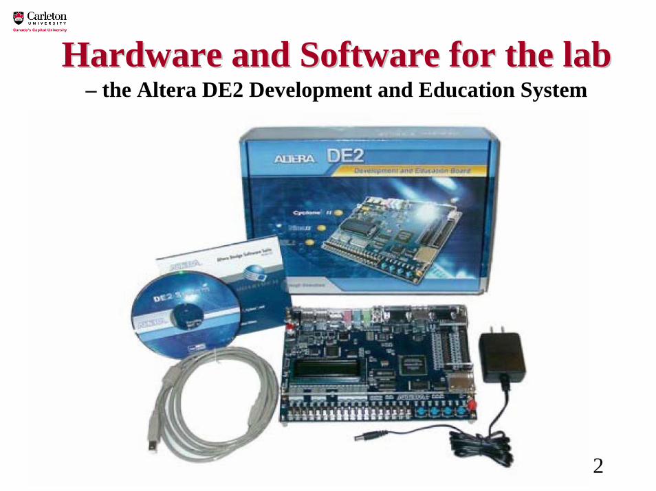
Hardware and Software for the labHardware and Software for the lab– the Altera DE2 Development and Education System
3
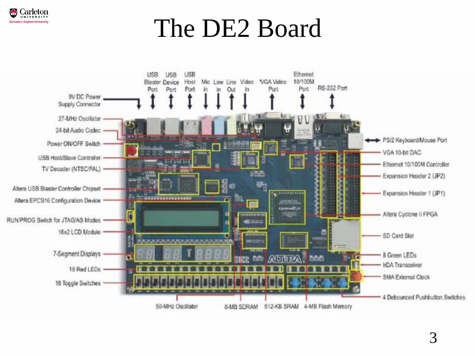
The DE2 Board
4
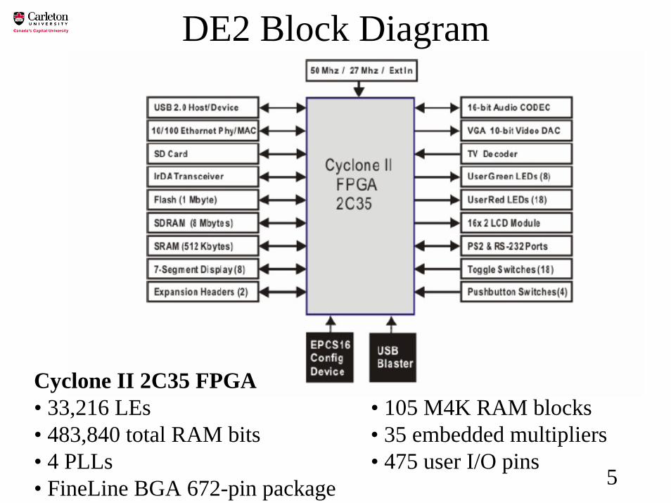
• Altera Cyclone® II 2C35 FPGA device• Altera Serial Configuration device - EPCS16• USB Blaster (on board) for programming and user API control• (AS) programming modes are supported• 512-Kbyte SRAM• 8-Mbyte SDRAM• 4-Mbyte Flash memory (1 Mbyte on some boards)• SD Card socket• 4 pushbutton switches• 18 toggle switches• 18 red user LEDs• 9 green user LEDs• 50-MHz oscillator and 27-MHz oscillator for clock sources• 24-bit CD-quality audio CODEC with line-in, line-out, and microphone-in jacks• VGA DAC (10-bit high-speed triple DACs) with VGA-out connector• TV Decoder (NTSC/PAL) and TV-in connector• 10/100 Ethernet Controller with a connector• USB Host/Slave Controller with USB type A and type B connectors• RS-232 transceiver and 9-pin connector• PS/2 mouse/keyboard connector• IrDA transceiver• Two 40-pin Expansion Headers with diode protection
5
DE2 Block Diagram
Cyclone II 2C35 FPGA• 33,216 LEs • 105 M4K RAM blocks• 483,840 total RAM bits • 35 embedded multipliers• 4 PLLs • 475 user I/O pins• FineLine BGA 672-pin package

6
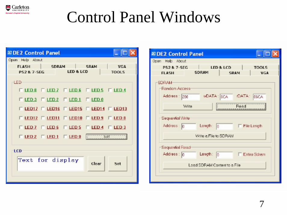
DE2 Control Panel
7
Control Panel Windows

8
Control Panel Block Diagram
9
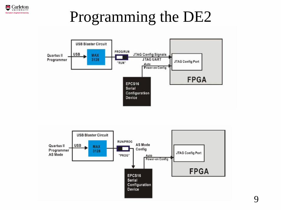
Programming the DE2
10
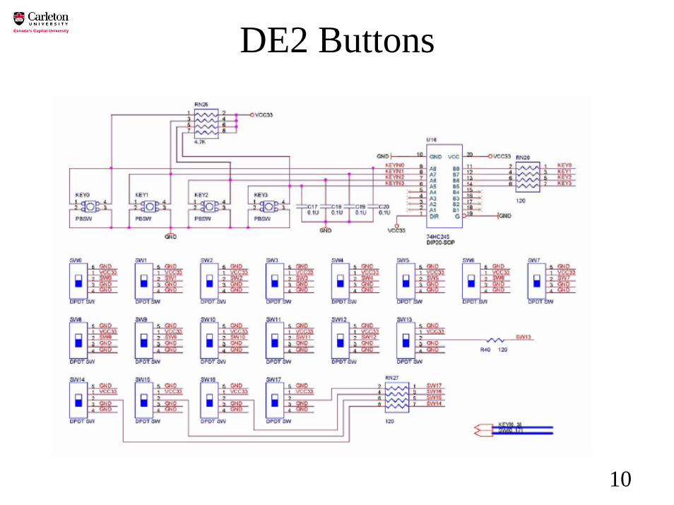
DE2 Buttons
11
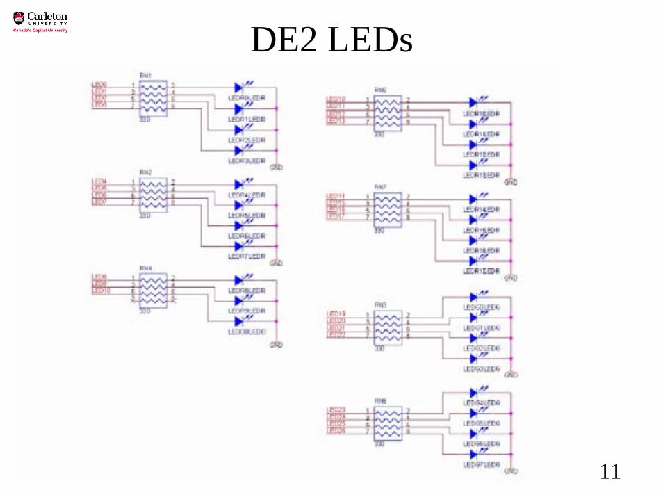
DE2 LEDs
12
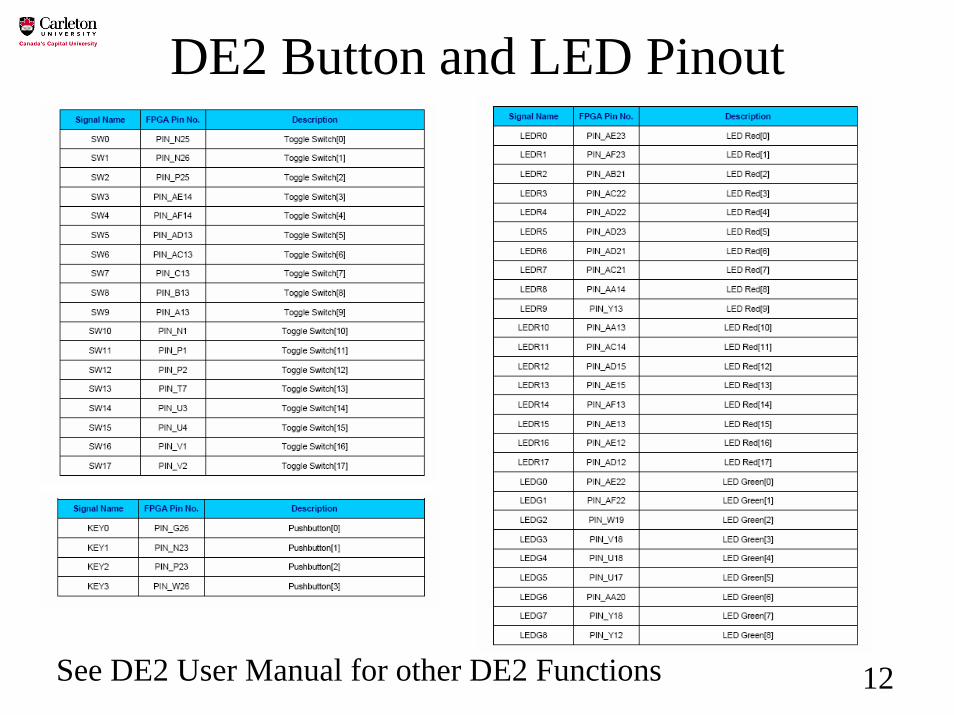
DE2 Button and LED Pinout
See DE2 User Manual for other DE2 Functions
13
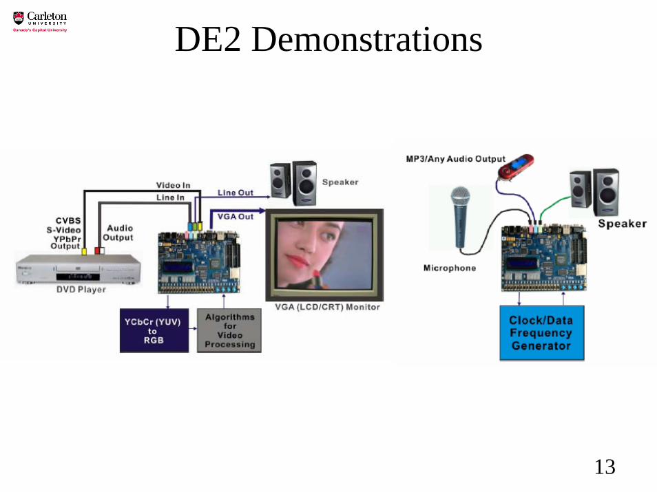
DE2 Demonstrations

14
FPGA Design Flow
15
• Design Entry – the desired circuit is specified either by means of a schematicdiagram, or by using a hardware description language, such as Verilog or VHDL
• Synthesis – the entered design is synthesized into a circuit that consists of the logic elements (LEs) provided in the FPGA chip
• Functional Simulation – the synthesized circuit is tested to verify its functional correctness; this simulation does not take into account any timing issues
• Fitting – the CAD Fitter tool determines the placement of the LEs defined in the netlist into the LEs in an actual FPGA chip; it also chooses routing wires in the chip to make the required connections between specific LEs
• Timing Analysis – propagation delays along the various paths in the fitted circuit are analyzed to provide an indication of the expected performance of the circuit
• Timing Simulation – the fitted circuit is tested to verify both its functional correctness and timing
• Programming and Configuration – the designed circuit is implemented in a physical FPGA chip by programming the configuration switches that configure the LEs and establish the required wiring connections
16
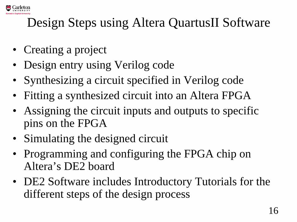
Design Steps using Altera QuartusII Software
• Creating a project• Design entry using Verilog code• Synthesizing a circuit specified in Verilog code• Fitting a synthesized circuit into an Altera FPGA• Assigning the circuit inputs and outputs to specific
pins on the FPGA• Simulating the designed circuit• Programming and configuring the FPGA chip on
Altera’s DE2 board• DE2 Software includes Introductory Tutorials for the
different steps of the design process