Embed Size (px)
Citation preview

13
Reticle Floorplanning and Simulated Wafer Dicing for Multiple-project Wafers
by Simulated Annealing
Rung-Bin Lin, Meng-Chiou Wu and Shih-Cheng Tsai Computer Science and Engineering, Yuan Ze University
Taiwan
1. Introduction
As semiconductor process technology relentlessly advances into deeper submicron feature sizes following the Moore’s Law, the cost of mask tooling is growing inexorably, up to 1, 1.5, and 3 million dollars for 90nm, 65nm, and 32nm process technology, respectively (LaPedus, 2006). Basically, the majority of smaller fabless integrated circuit (IC) design houses can hardly afford to have one mask set per design just for prototyping or low-volume production. In this circumstance, multiple project wafer (MPW) fabrication (or called shuttle run), long being used as a low-cost mechanism by the academics or industries (Pina, 2001; Morse, 2003) for prototyping their innovative designs, has become an indispensable chip fabrication vehicle. By way of an MPW program, the mask cost can be amortized among various designs placed in the same reticle (i.e., the same mask). Despite of assuming a lower mask cost per design, MPW requires each design to share more wafer fabrication cost. To minimize MPW wafer fabrication cost, the chips participating in a shuttle run should be properly placed in a reticle. This gives rise to the reticle floorplanning problem. Moreover, the wafers must be properly sawn to maximize the dicing yield. This gives rise to the simulated wafer dicing problem. In this chapter, we propose several approaches based on simulated annealing (SA) to solving reticle floorplanning and simulated wafer dicing problems. Since SA’s introduction (Kirkpatrick et al., 1983), it has played an important role in electronic design automation (Wong et al., 1988) such as circuit partitioning, placement, routing, etc. Many commercial physical design tools of this sort often employ SA as the last resort to optimize a design. The reasons for using SA are due to its ease of handling hard-to-be-satisfied constraints by transforming them into part of the objective function and a higher probability of finding a global optimum solution enabled by the capability of escaping local optima in practical implementations. Besides, an objective function for SA can be non-analytic or even does not have a closed-form expression so that it can only be evaluated using a non-calculus approach. Our simulated wafer dicing problem, though not having any hard-to-be-satisfied constraints, has a non-analytic objective function which makes SA quite suitable for solving this problem. Our reticle floorplanning problem has an even more difficult objective function which is the number of wafers required to be fabricated for a shuttle run and can only be evaluated using simulated wafer dicing. Despite of being able to handle non-O
pen
Acc
ess
Dat
abas
e w
ww
.i-te
chon
line.
com
Source: Simulated Annealing, Book edited by: Cher Ming Tan, ISBN 978-953-7619-07-7, pp. 420, February 2008, I-Tech Education and Publishing, Vienna, Austria
www.intechopen.com

Simulated Annealing
258
analytic objective function, SA should not employ a hard-to-be-evaluated objective function because it would take too much time just to calculate the objective function for each new solution generated in the search process. To cope with this difficulty, we need to find a simple objective function that can best correspond to the original one, i.e., transforming the original objective function into a simpler one. Therefore, rather than solving a complicate simulated wafer dicing problem, we devise a much simpler objective function for our reticle floorplanning problem. Although we can not guarantee an exact correspondence between optimal solutions in the original problem and the one with a simpler objective function, such a transformation generally enables us to find a sufficiently good solution in a short time. Another key factor to successful applications of SA is about solution encoding. If a solution encoding could theoretically make SA reach every solution in the solution space, such solution encoding is certainly the best. However, if a solution encoding can not make this happen, the subspace defined by such solution encoding should include at least one global optimum. Unfortunately, we normally do not have such kind of insight. The two solution encodings used for our reticle floorplanning are no exception. However, both of them have their own edges. One enables SA to find a solution with a minimum number of wafers fabricated, whereas the other enables SA to find a solution with a smaller reticle area and with the number of required wafers very close to that of the former. The experimental results show that our approach when compared to the previous work (Kahng et al., 2005) not only achieves a double-digit saving in the number of wafers fabricated per shuttle run, but also produces a reticle floorplan with considerably smaller reticle area. This means a lot of saving in mask tooling and wafer fabrication costs. Although minimizing the number of wafers fabricated in a shuttle run is often a good objective for reticle floorplanning, a minimum wafer use does not necessarily mean a minimum-cost wafer fabrication (not including mask tooling cost), not to mention a minimum-cost shuttle production (including mask tooling cost). Reticle floorplanning for cost minimization is a multiple objective optimization problem where the mask tooling and wafer fabrication costs are two conflicting goals (Bonn, 2001). Minimizing mask tooling cost favors a smaller reticle size (the smaller the reticle, the less the mask tooling cost, as shown in Figure 1), but this would pack chips closely within a reticle and hence create excessive sawing conflicts. As a consequence, more wafers must be fabricated. On the other hand, an attempt to align chips in a reticle to reduce sawing conflicts often requires a larger reticle and hence increases the mask tooling cost. Our reticle floorplanning method has a coefficient in the SA’s objective function that can be explored to find a solution balancing these two objectives. We have employed our reticle floorplanning and simulated wafer dicing methods to perform a reticle design space exploration for finding a minimum-cost solution (Lin et al., 2007). In this article, we will not discuss this issue any further. Our presentation will focus on using SA for solving reticle floorplanning and simulated wafer dicing problems with an objective of minimizing the number of wafers fabricated. A lot of the material presented here can also be found in our previous work (Lin et al., 2007; Wu & Lin, 2007; Wu et al., 2008). For ease of presentation, we will use chip, project, and design interchangeably in this article. The rest of this chapter is organized as follows. In Section 2, we elaborate on simulated
wafer dicing and reticle floorplanning problems and their related work. In Sections 3 and 4,
we present our SA implementations for these two problems, respectively. In Section 5, we
draw a conclusion for our work.
www.intechopen.com

Reticle Floorplanning and Simulated Wafer Dicing for Multiple-project Wafers by Simulated Annealing
259
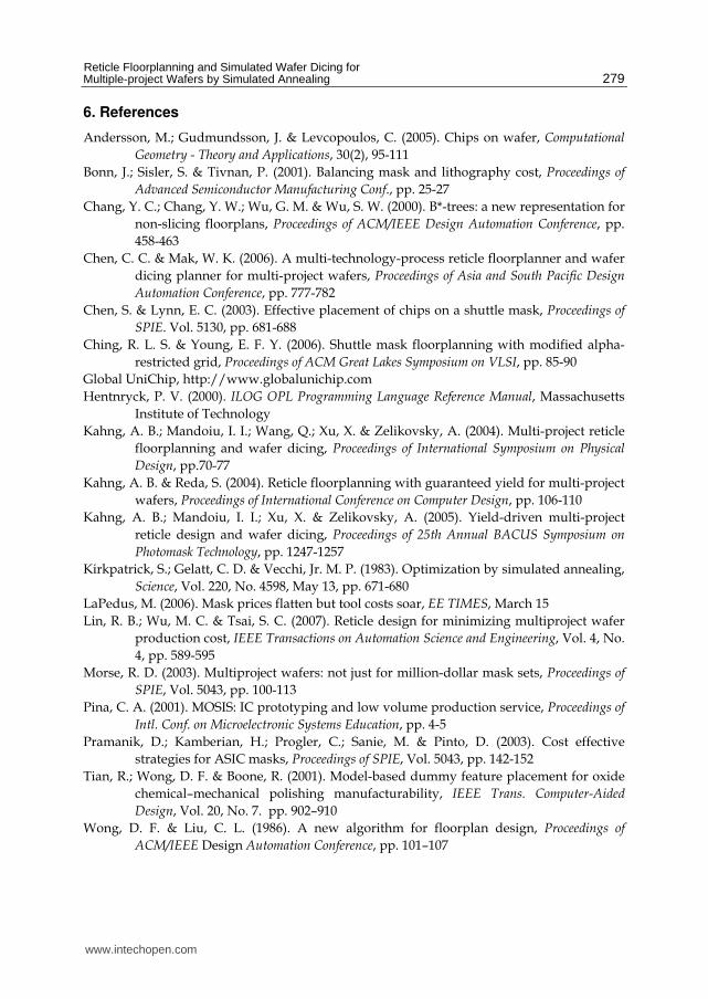
Fig. 1. Mask set cost for various field sizes for a 90nm technology node assuming that a chip has 8 very critical layers, 8 critical layers, and 12 non-critical layers (Pramanik et al., 2003)
2. Problem definition and related work
2.1 Problem definition Here, we will give a problem definition of simulated wafer dicing and reticle floorplanning
problems, respectively. Before doing this, we briefly describe how an MPW wafer is
fabricated. Figure 2 shows a simplified wafer lithography apparatus. A reticle is placed
between a condensing and a projection lens. The patterns in the reticle are exposed to the
light so that a copy of these patterns can be transferred to the wafer during exposure. We
call the region that has the patterns formed per exposure a field. The above process is
repetitively executed to form an array of fields on a wafer. Normally, there is a 4X or 5X
reduction in dimensions for the patterns printed on the wafer, i.e., the field dimensions are
1/4 or 1/5 of the reticle dimensions.
Prior to wafer fabrication, we need to know the number of wafers that must be fabricated. If
a reticle contains multiple copies of the layout design for only one chip, these copies are
normally arranged into an m-by-n matrix so that the number of wafers that must be
fabricated can be easily determined. However, this cannot be done easily for MPWs because
the chips in a reticle cannot usually be arranged into an m-by-n matrix, as shown on the left
of Figure 3. In this situation, wafer sawing done to obtain dice for a chip may destroy many
dice for other chips. This complicates the calculation for the number of wafers that must be
fabricated. Therefore, simulated wafer dicing must be performed to determine the number
of required wafers. In simulated wafer dicing, wafer sawing is tentatively performed on an
MPW to determine which dice will be obtained. Normally, a sawing line must run across
from one side of a wafer to the other side of the wafer, without stopping at the middle of the
wafer. This requirement is called the side-to-side dicing constraint. To yield a good die, sawing
should be performed at each of the four borders of a die with no other sawing line running
across it. The example in Figure 3 shows that we can employ sawing lines v1, v2, v3, h1, h2,
and h3 to obtain three good bare dice respectively for chips 4, 5, and 8, but this also destroys
www.intechopen.com

Simulated Annealing
260
the dice for chips 6, 7, and 10. Although the dice for chips 1, 2, 3, and 9 are not destroyed,
they are discarded due to a difficulty packaging them. The sawing lines made for a reticle
(field) form a reticle dicing plan. All of the reticle dicing plans used for sawing a wafer form a
wafer dicing plan (Kahng et al., 2004). Because of the side-to-side dicing constraint, all of the
fields on the same row (column) will have the same horizontal (vertical) dicing plan. The
problem is how to choose a set of reticle dicing plans to maximize dicing yield per wafer
and thus minimize the number of wafers fabricated for a shuttle run. Figure 4(a) shows a
wafer dicing plan that yields six dice per wafer respectively for the four chips 1, 2, 3, and 4
contained in a reticle. Given that the required production volumes are 24, 48, 24, and 48 dice
for chips 1, 2, 3, and 4, respectively, the number of wafers needed is eight. However, the
number of wafers is reduced to six if the wafer dicing plan in Figure 4(b) is used. The
simulated wafer dicing problem is formally defined below.
Simulated Wafer Dicing Problem (SWDP): Given a reticle floorplan of N chips and the required production volume Vp for chip p, p=1..N, determine the wafer dicing plan for each of the Q wafers under the side-to-side dicing constraint such that the number Bp of good bare dice is greater than or equal to Vp and Q is minimized.
Fig. 2. Wafer lithography
www.intechopen.com

Reticle Floorplanning and Simulated Wafer Dicing for Multiple-project Wafers by Simulated Annealing
261
Fig. 3. A multi-project wafer
Fig. 4. Two wafer dicing plans (good dice in darker color (green))
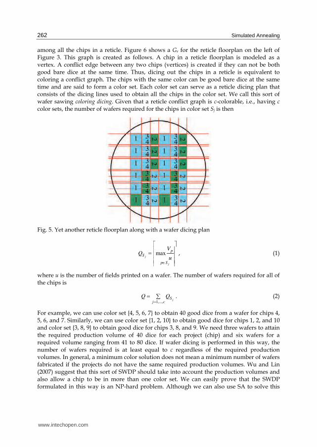
Reticle floorplanning determines the positions of the chips in a reticle and thus has a profound effect on dicing yield. Figure 5 shows another reticle floorplan along with a dicing plan for the same chips given in Figure 4. This reticle floorplan has a smaller size, but the dicing plan yields only 2, 6, 4, and 4 dice per wafer for the four chips, respectively. For the same required production volumes as above, 12 wafers need to be fabricated. As one can see, reticle floorplanning has a great influence on the number of required wafers. Our reticle floorplanning problem is formally defined below. Reticle Floorplanning Problem (RFP): Given a set of N chips and their required production volumes Vp, p=1..N, determine the coordinates of the chips such that the number of wafers used to attain the required production volumes of these chips is minimized on the condition that no chips overlap and all the chips are inside the reticle whose dimensions are not larger than the maximally permissible values.
2.2 Related work for SWDP In the past, a few simulated wafer dicing methods have been proposed (Xu et al., 2004; Kahng et al., 2004; Chen & Mak, 2006). These methods, distinguished by the ways of satisfying required production volumes, are classified into two groups. The first group, as suggested in (Xu et al., 2004), uses a reticle conflict graph Gr to describe the dicing conflicts
www.intechopen.com
Simulated Annealing
262
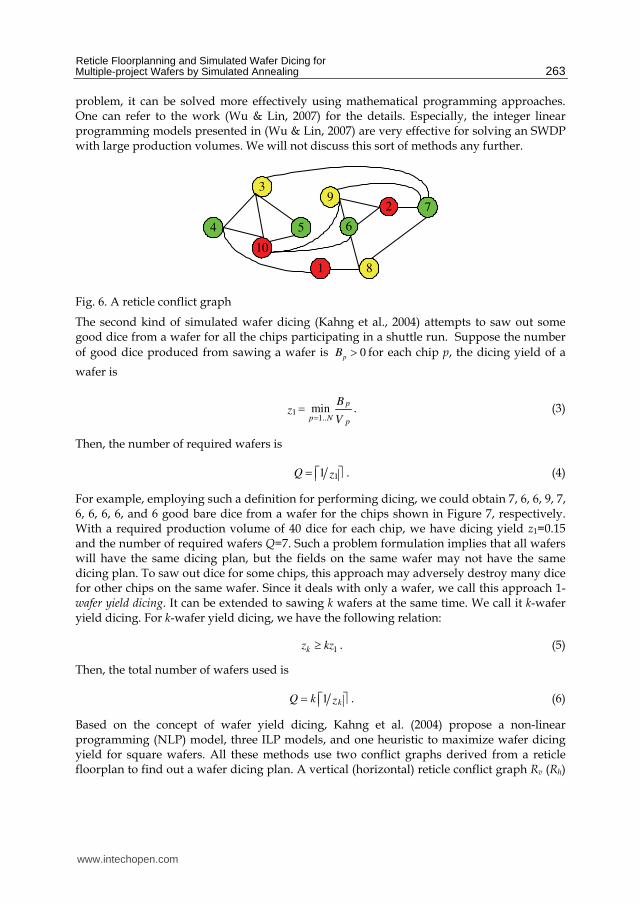
among all the chips in a reticle. Figure 6 shows a Gr for the reticle floorplan on the left of Figure 3. This graph is created as follows. A chip in a reticle floorplan is modeled as a vertex. A conflict edge between any two chips (vertices) is created if they can not be both good bare dice at the same time. Thus, dicing out the chips in a reticle is equivalent to coloring a conflict graph. The chips with the same color can be good bare dice at the same time and are said to form a color set. Each color set can serve as a reticle dicing plan that consists of the dicing lines used to obtain all the chips in the color set. We call this sort of wafer sawing coloring dicing. Given that a reticle conflict graph is c-colorable, i.e., having c color sets, the number of wafers required for the chips in color set Sj is then
Fig. 5. Yet another reticle floorplan along with a wafer dicing plan
maxj
j
p
S
p S
VQ
u∈
⎡ ⎤⎢ ⎥= ⎢ ⎥⎢ ⎥⎢ ⎥, (1)
where u is the number of fields printed on a wafer. The number of wafers required for all of the chips is
1,...,
jSj c
Q Q== ∑ . (2)
For example, we can use color set {4, 5, 6, 7} to obtain 40 good dice from a wafer for chips 4, 5, 6, and 7. Similarly, we can use color set {1, 2, 10} to obtain good dice for chips 1, 2, and 10 and color set {3, 8, 9} to obtain good dice for chips 3, 8, and 9. We need three wafers to attain the required production volume of 40 dice for each project (chip) and six wafers for a required volume ranging from 41 to 80 dice. If wafer dicing is performed in this way, the number of wafers required is at least equal to c regardless of the required production volumes. In general, a minimum color solution does not mean a minimum number of wafers fabricated if the projects do not have the same required production volumes. Wu and Lin (2007) suggest that this sort of SWDP should take into account the production volumes and also allow a chip to be in more than one color set. We can easily prove that the SWDP formulated in this way is an NP-hard problem. Although we can also use SA to solve this
www.intechopen.com
Reticle Floorplanning and Simulated Wafer Dicing for Multiple-project Wafers by Simulated Annealing
263
problem, it can be solved more effectively using mathematical programming approaches. One can refer to the work (Wu & Lin, 2007) for the details. Especially, the integer linear programming models presented in (Wu & Lin, 2007) are very effective for solving an SWDP with large production volumes. We will not discuss this sort of methods any further.
3
4 5
10
2
6
9
8
7
1
Fig. 6. A reticle conflict graph
The second kind of simulated wafer dicing (Kahng et al., 2004) attempts to saw out some good dice from a wafer for all the chips participating in a shuttle run. Suppose the number
of good dice produced from sawing a wafer is 0p
B > for each chip p, the dicing yield of a
wafer is
11..
minp
p N p
Bz
V== . (3)
Then, the number of required wafers is
11Q z= ⎡ ⎤⎢ ⎥ . (4)
For example, employing such a definition for performing dicing, we could obtain 7, 6, 6, 9, 7, 6, 6, 6, 6, and 6 good bare dice from a wafer for the chips shown in Figure 7, respectively. With a required production volume of 40 dice for each chip, we have dicing yield z1=0.15 and the number of required wafers Q=7. Such a problem formulation implies that all wafers will have the same dicing plan, but the fields on the same wafer may not have the same dicing plan. To saw out dice for some chips, this approach may adversely destroy many dice for other chips on the same wafer. Since it deals with only a wafer, we call this approach 1-wafer yield dicing. It can be extended to sawing k wafers at the same time. We call it k-wafer yield dicing. For k-wafer yield dicing, we have the following relation:
1kz kz≥ . (5)
Then, the total number of wafers used is
1 kQ k z= ⎡ ⎤⎢ ⎥ . (6)
Based on the concept of wafer yield dicing, Kahng et al. (2004) propose a non-linear programming (NLP) model, three ILP models, and one heuristic to maximize wafer dicing yield for square wafers. All these methods use two conflict graphs derived from a reticle floorplan to find out a wafer dicing plan. A vertical (horizontal) reticle conflict graph Rv (Rh)
www.intechopen.com

Simulated Annealing
264
can be created in a manner similar to a reticle conflict graph, only considering the dicing conflicts created by the vertical (horizontal) dicing lines among the chips in a reticle. An independent set in a Rv (Rh) defines a set of vertical (horizontal) dicing lines that can be used simultaneously to saw out all the chips in the independent set without destroying each other. Thus, to saw out as many chips as possible, a maximal independent set should be employed.
Fig. 7. Wafer dicing yield (good dice in darker color (green))
Fig. 8. A vertical reticle conflict graph
Fig. 9. A horizontal reticle conflict graph
A reticle dicing plan can be obtained by intersecting a maximal independent set in Rv with a maximal independent set in Rh. Those chips belonging to the intersection will be good bare dice if the reticle dicing plan defined by the chips in the intersection is used. For example, given the vertical reticle conflict graph in Figure 8 and horizontal reticle conflict graph in Figure 9, the intersection of maximal vertical independent set {2,3,8} with maximal horizontal independent set {1,2,5,7,8,10} is {2,8}. Thus, chips 2 and 8 can be good bare dice at
www.intechopen.com

Reticle Floorplanning and Simulated Wafer Dicing for Multiple-project Wafers by Simulated Annealing
265
the same time. It is worth noting that the intersection {2,8} is not a maximal independent set in the reticle conflict graph in Figure 6. Because of this, a simulated wafer dicing method using maximal independent sets in Rv and Rh may fail to produce a good wafer dicing plan. It is likely that an intersection is empty. For example, the intersection of maximal vertical independent set {1,3,9} with maximal horizontal independent set {2,4,5,7,8,10} is empty. Apparently, wafer yield dicing is quite different from coloring dicing. Wafer yield dicing requires that at least one good bare die be produced from the wafers sawn. This may generate a large number of different reticle dicing plans on a wafer. On the contrary, coloring dicing normally generate the same reticle dicing plan for all the fields in a wafer and produces the dice only for the chips in a color set. The consequence of this difference is that wafer yield dicing can result in a smaller number of wafers fabricated for low-volume production. For high-volume production, both approaches perform equally well, but wafer-yield dicing is more time consuming. In this article, we will present a wafer yield dicing method based on SA using maximal independent sets derived from vertical and horizontal conflict graphs.
2.3 Related work for RFP In the past, many reticle floorplanning methods have been proposed. These methods can generally be classified into the following groups.
• Slicing tree packing Chen and Lynn (2003) perform reticle floorplanning using slicing trees (Wong & Liu, 1986) for reticle area minimization. Xu et al. (2003) employ slicing trees to perform reticle area minimization while taking die-to-die inspection into consideration. Xu et al. (2004; 2005) further consider metal density optimization (Tian et al., 2001) to improve wafer planarization. These methods consider only reticle area minimization.
• Shelf-packing Kahng et al. (2004) propose a shelf-packing heuristic that places chips in several shelves. A so-obtained solution is improved by simulated annealing interlacing with a dicing heuristic to maximize dicing yield while minimizing reticle area. Several mathematical programming models for determining wafer dicing lines are also presented there. However, this work considers only square wafers.
• Grid floorplan
Andersson et al. (2003) propose to pack chips into a two-dimensional array of grids, each of which holds at most one chip such that chips can be aligned in horizontal and vertical directions. Kahng and Reda (2004) propose a branch-and-bound algorithm to find a grid floorplan with the largest dicing yield. This work considers only square wafers. Chen and Mak (2006) propose a method to solve a reticle floorplanning problem for chips using a different number of metal layers. Ching and Young (2006) define a special type of grid, called modified alpha-restricted grid, to reduce the size of the solution space for grid floorplan.
• Hierarchal quadrisection floorplanning Kahng et al. (2005) further propose a hierarchal quadrisection reticle floorplanning method based on simulated annealing which directly minimizes the upper bound on the number of required wafers. A shot-map optimization method is exploited to define the fields printed on a wafer. We will elaborate on this approach later since one of our reticle floorplanning methods is closely related to it.
www.intechopen.com
Simulated Annealing
266
Besides the aforementioned works, Wu and Lin (2005) propose a non-linear programming
model for solving a reticle floorplanning problem with flexible chip dimensions. Wu et al.
(2006) also propose a method based on B*-tree (Chang et al., 2000) for solving multiple
reticles floorplanning problem.
3. Simulated wafer dicing by simulated annealing
Our simulated annealing implementation for SWDP has its root from an efficient heuristic
called Iterative Augment and Search Algorithm (IASA) presented by Kahng et al. (2004).
IASA first assigns a vertical (horizontal) reticle dicing plan for each of the first cv columns of
fields (the first ch rows of fields), where cv (ch ) is the minimum number of colors used to
color a vertical (horizontal) reticle conflict graph. These vertical (horizontal) reticle dicing
plans are derived from a minimum coloring of a vertical (horizontal) reticle conflict graph.
Vertical (horizontal) dicing plans, i.e., maximal vertical (horizontal) independent sets that
maximize wafer dicing yield are then one-by-one respectively assigned to the remaining
columns (rows) until all the columns (rows) have their own dicing plans. Before assigning a
vertical (horizontal) dicing plan to one of the remaining columns (rows), the dicing plans of
the already assigned columns (rows) each are replaced by a dicing plan that can attain the
largest yield. This step is repeated until dicing yield can not be further improved. IASA can
find a wafer dicing plan very fast, but it tends to be greedy. In the next subsection, we will
elaborate on our SA method for solving this problem.
3.1 Simulated annealing implementation Here, we will introduce a k-wafer yield dicing method based on SA. This method is called
HVMIS-SA-Z. Our method has its root from IASA. It also employs maximal vertical and
horizontal independent sets. A typical SA is responsible for choosing a viable k-wafer dicing
plan. Figure 10 gives the pseudo code for HVMIS-SA-Z. The objective function directly
maximizes k-wafer dicing yield zk. Our neighbourhood function generates a new solution by
randomly replacing the dicing plan of a column (row) with a new dicing plan selected from
the set of maximal vertical (horizontal) independent sets. The column (row) being replaced
with a new dicing plan could be any column (row) on any of the k wafers. It takes some trick
to update k-wafer dicing yield for a new solution. We need only to recalculate the number of
good bare dice produced from the column (row) selected for being replaced with a new
dicing plan. Solution encoding for SWDP is trivial, i.e., a column (row) is simply assigned a
maximal vertical (horizontal) independent set. This solution encoding can represent each of
the solutions in the solution space of the k-wafer yield dicing problem. The neighborhood
function also makes our SA with a non-zero probability of reaching every solution in the
solution space. SA terminates if no better dicing plan is found for a number of consecutive
inner while loops.
The reason for exploring k-wafer yield dicing is that 11/ z⎡ ⎤⎢ ⎥ can be a very poor estimator
(upper bound) for the number of required wafers as it can be observed from the work done
by Wu & Lin (2007). We have two ways of performing k-wafer yield dicing. First, we can use
HVMIS-SA-Z to find a smallest k so that 1kz ≥ . The problem is that we would need to
repeat running HVMIS-SA-Z for all possible k’s values. This is very time consuming if the
www.intechopen.com

Reticle Floorplanning and Simulated Wafer Dicing for Multiple-project Wafers by Simulated Annealing
267
required production volumes are large. Second, we use HVMIS-SA-Z to compute / kk z⎡ ⎤⎢ ⎥
for k from one up to a certain value (10, for example). We then select a k’s value that has the
smallest / ky k z= ⎡ ⎤⎢ ⎥ . We repeatedly run HVMIS-SA-Z to obtain zy and a new y with
/ ky k z= ⎡ ⎤⎢ ⎥ until a smallest y that makes 1yz ≥ can be attained. In this manner, HVMIS-SA-Z
can find a better solution more efficiently for a problem with large production volumes. The
reason why this works effectively is because / kk z⎡ ⎤⎢ ⎥ rather than 1/ kz⎡ ⎤⎢ ⎥ is a good bound on
the number of wafers used. The data in the column denoted by HVMIS-SA-Z in Table 2 are
obtained using such an approach.
Fig. 10. Simulated annealing implementation for SWDP
void HVMIS-SA-Z(k, FR, PV) {
//FR: a given reticle floorplan for a shuttle run.
//PV: required production volumes for all the chips in a shuttle run
//k: number of wafers sawn simultaneously
double zk, zkn, best_zk; // k-wafer dicing yield
set MHIS, MVIS; // sets of maximal horizontal and vertical independent set, respectively
k_wafer_dicing_plan best_dp, current_dp, next_dp;
double T; // temperature
double alpha=0.95;
int frozen( ), equilibrium( );
MHIS=find_maximal_horizontal_indepedent_set(FR);
MVIS=find_maximal_vertical_indepedent_set(FR);
current_dp=find_initial_dicing_plan(k, MHIS, MVIS);
zk=calculate_k_wafer_dicing_yield(current_dp, PV);
best_dp=current_dp;
T=determine_initial_temperature(k,MHIS, MVIS);
while(not frozen( )){
while(not equilibrium( )){
next_dp=generate_next_wafer_dicing_plan(current_dp, MHIS, MVIS);
zkn= calculate_k_wafer_dicing_yield(next_dp, PV);
if(zkn>zk){
current_dp=next_dp;
zk=zkn;
if(zkn>best_zk){
best_zk=zkn;
best_dp=next_dp;}}
else if( ( )zkn zk
Trandom e−< ){
current_dp=next_dp;
zk=zkn; }
}
T=alpha*T;
}
return(best_dp, best_zk);
}
www.intechopen.com
Simulated Annealing
268
3.2 Experimental results for simulated wafer dicing Here, we perform some experiments with two wafer dicing approaches: IASA and HVMIS-
SA-Z. We first investigate which dicing method could attain the largest 1-wafer dicing yield.
We then make a comparison between IASA (Kahng et al., 2004) and k-wafer yield dicing. All
experiments are executed on a 2.8 GHz Pentium 4 CPU with 512Mb memory. We use MILP-
VOCO proposed in Wu et al. (2008) to obtain the reticle floorplans for all the test cases. Our
study is made on 200mm (8 inches) and 300mm (12 inches) wafers.
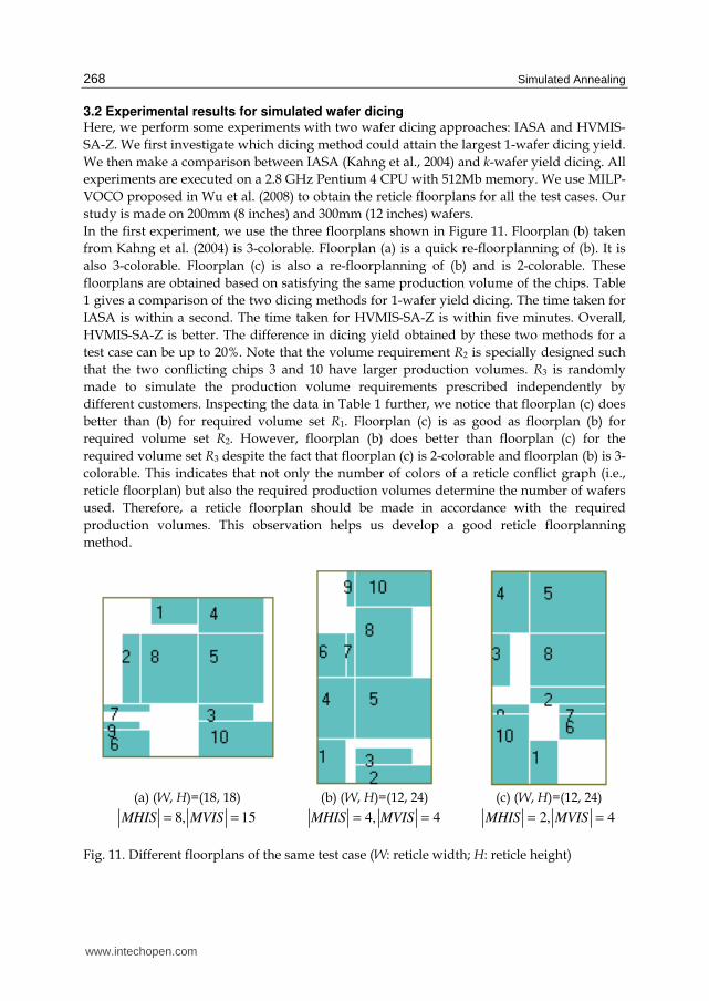
In the first experiment, we use the three floorplans shown in Figure 11. Floorplan (b) taken
from Kahng et al. (2004) is 3-colorable. Floorplan (a) is a quick re-floorplanning of (b). It is
also 3-colorable. Floorplan (c) is also a re-floorplanning of (b) and is 2-colorable. These
floorplans are obtained based on satisfying the same production volume of the chips. Table
1 gives a comparison of the two dicing methods for 1-wafer yield dicing. The time taken for
IASA is within a second. The time taken for HVMIS-SA-Z is within five minutes. Overall,
HVMIS-SA-Z is better. The difference in dicing yield obtained by these two methods for a
test case can be up to 20%. Note that the volume requirement R2 is specially designed such
that the two conflicting chips 3 and 10 have larger production volumes. R3 is randomly
made to simulate the production volume requirements prescribed independently by
different customers. Inspecting the data in Table 1 further, we notice that floorplan (c) does
better than (b) for required volume set R1. Floorplan (c) is as good as floorplan (b) for
required volume set R2. However, floorplan (b) does better than floorplan (c) for the
required volume set R3 despite the fact that floorplan (c) is 2-colorable and floorplan (b) is 3-
colorable. This indicates that not only the number of colors of a reticle conflict graph (i.e.,
reticle floorplan) but also the required production volumes determine the number of wafers
used. Therefore, a reticle floorplan should be made in accordance with the required
production volumes. This observation helps us develop a good reticle floorplanning
method.
(a) (W, H)=(18, 18)
8, 15MHIS MVIS= =
(b) (W, H)=(12, 24)
4, 4MHIS MVIS= =
(c) (W, H)=(12, 24)
2, 4MHIS MVIS= =
Fig. 11. Different floorplans of the same test case (W: reticle width; H: reticle height)
www.intechopen.com

Reticle Floorplanning and Simulated Wafer Dicing for Multiple-project Wafers by Simulated Annealing
269
200mm wafer 300mm wafer Required volumes
FloorplanIASA (Kahng et
al., 2004) HVMIS-SA-Z
IASA (Kahng etal., 2004)
HVMIS-SA-Z
(a) 0.35 0.38 0.80 0.93
(b) 0.63 0.68 1.43 1.55
R1=(40,40,40,40,40,40,40,
40,40,40) (c) 0.70 0.78 1.65 1.75
(a) 0.19 0.23 0.52 0.60
(b) 0.35 0.42 0.86 0.93
R2=(40,40,80,40,40,40,40,40,40,120) (c) 0.38 0.40 0.79 0.91
(a) 0.13 0.15 0.31 0.36
(b) 0.20 0.23 0.48 0.51
R3=(170,60,30,60,100,70,110,140,100,2
10) (c) 0.17 0.20 0.44 0.45
Table 1. 1-wafer dicing yield for the three floorplans given in Figure 11
I4: (W, H)= (13.1,13.1)
Required volumes: 60, 60, 200, 200, 400, 400, 600,
600
I5: (W, H)= (10,10) Required volumes:
100, 200, 300, 200, 200, 200, 200, 200, 80, 60
I6: (W, H)= (18,19.9) Required volumes:
60, 100, 120, 120, 160, 160, 200, 200, 200, 200, 200, 200,
200
Fig. 12. Floorplans for the three industry test cases
Table 2 shows the number of wafers used (columns denoted by #wf) and the times taken by wafer yield dicing methods for the three industrial test cases shown in Figure 12 and the test case in Figure 11(c) with the required volume set R1. The three industrial test cases are obtained from Global UniChip. To see how these methods scale with the production volumes, we scale the required volumes by a factor of 5, 10, 100, and 1000. HVMIS-SA-Z attains better results for larger production volumes. Compared to IASA (Kahng et al., 2004), HVMIS-SA-Z could achieve up to 50% wafer reduction for some cases. It achieves on average 18% and 37% fewer wafers for low and high volume productions, respectively. The data for IASA are obtained using 1-wafer yield dicing. The time spent for obtaining each datum for IASA is that for finding out 1-wafer dicing yield z1 defined in (3). Figure 13 shows a wafer dicing plan for one of the two wafers obtained by HVMIS-SA-Z for I4. As one can see, several different reticle dicing plans have been created to generate some dice for each of the chips in the reticle.
www.intechopen.com

Simulated Annealing
270
IASA (Kahng et al., 2004) HVMIS-SA-Z Floorplan
Required volumes #wf t(sec.) #wf t(sec.)
1X 1 0 1 8
5X 4 0 2 19
10X 7 0 4 44
100X 61 0 39 121
Figure 11(c) with required volume set R1
1000X 607 0 385 500
1X 2 0 2 20
5X 8 0 8 67
10X 16 0 16 89
100X 160 0 160 161
I4
1000X 1596 0 1596 1101
1X 2 1 2 41
5X 10 1 6 122
10X 19 1 11 216
100X 189 1 110 1398
I5
1000X 1887 1 1095 1301
1X 6 0 4 62
5X 28 0 16 105
10X
100X
56 556
0 0
31 297
148 1028
I6
1000X 5556 0 2959 1102
1X 0% 18%
5X 0% 36%
10X 0% 37%
100X 0% 37%
Average reduction
1000X 0% 37%
Table 2. Simulated wafer dicing for various production volumes
4. Reticle floorplanning by simulated annealing
In this section we first review two solution encodings used in our SA for RFP. We then describe a simple objective function for approximating the most accurate objective function used for RFP. One may recall that the most accurate objective function for RFP is the number of required wafers, which can only be obtained using a simulated wafer dicing method. The simulated wafer dicing method IASA described in Section 3 is originally used for such a purpose. Finally, we will describe how SA is implemented to solve RFP.
4.1 Solution encoding We use B*-tree (Chang et al., 2000) as one of our solution encodings. B*-tree was originally designed for finding a minimum-area floorplan for an ASIC design. A B*-tree corresponds to a reticle floorplan. A node in a B*-tree represents a chip in a reticle. The chip
www.intechopen.com

Reticle Floorplanning and Simulated Wafer Dicing for Multiple-project Wafers by Simulated Annealing
271
corresponding to the root is placed at the bottom-left corner of a reticle. The chip corresponding to the left child j is abutted to the right of the chip corresponding to the parent node i with
j i ix x w= + . The chip corresponding to the right child is placed
immediately above the chip corresponding to the parent with the same x coordinate. Recursively traversing a whole tree using depth-first search from the root, we can convert a tree representation into a reticle floorplan. Once this is done, chips are normally pushed to the left and then to the bottom to form a compact floorplan. Figure 14 shows a B*-tree and its corresponding floorplan (without doing pushing). B*-tree can not represent non-compact floorplans in the solution space defined for RFP. This might have an impact on finding a solution that incurs the minimum use of wafers. However, its capability of obtaining a compact floorplan is important for mask tooling cost minimization as shown in Figure 1.
Fig. 13. A wafer dicing plan obtained by HVMIS-SA-Z for I4 with 1X volume ( good dice in darker color (green))
www.intechopen.com

Simulated Annealing
272
Fig. 14. A B*-tree and its corresponding floorplan
We also employ a solution encoding called hierarchical quadrisection (Kahng et al., 2005) in our work. Hierarchal quadrisection (HQ) recursively divides a reticle into four regions, each of which holds at most one chip. It partitions the chips into 2l disjoint subsets, where l is the number of levels in a hierarchy. As an example shown in Figure 15, the reticle is divided into 16 regions (i.e., l=2), each of which contains at most one chip. The four disjoint subsets are {2,3}, {4,8}, {1,6} and {5,7}. The chips in the same subset can be sawn out simultaneously. This representation was originally used in Kahng et al. (2005) to facilitate to compute an upper on the number of required wafers. This bound is then used as the objective function for a reticle floorplanning method based on SA. An SA implementation based on HQ outperforms the shelf-packing heuristic (Kahng et al., 2004) and the grid-floorplan-based branch-and-bound algorithm (Kahng & Reda, 2004) proposed by the same research group. As one can see, HQ can not represent compact floorplans. This is in contrast to B*-tree. Compactly packed floorplans obtained from B*-tree will incur a number of dicing conflicts. However, this drawback is compensated by having a smaller reticle size so that more fields will be printed on a wafer. On the contrary, non-compact floorplans obtained from HQ will create fewer conflicts but generally have lager reticle size.
Fig. 15. A hierarchical quadrisection floorplanning
4.2 Objective function The objective function for RFP is the number of wafers fabricated if the underlying reticle floorplan is employed for a shuttle run. However, the exact number of required wafers can
www.intechopen.com
Reticle Floorplanning and Simulated Wafer Dicing for Multiple-project Wafers by Simulated Annealing
273
only be obtained using simulated wafer dicing, which is too time consuming for an SA implementation. As one may recall, HQ can facilitate to construct a reticle floorplanning objective function which calculates an upper bound on the number of required wafers. Unfortunately, given a reticle floorplan the so-obtained bound is constantly far from the minimum number of required wafers. Other more accurate bounds are presented in Wu et al. (2008). However, the solution quality obtained using this sort of objective functions is not comparable to that obtained using our objective function. Our objective function is based on a simple observation that two chips should be placed at the positions where no dicing conflict between them can be created if their required production volumes are large. We call these two chips compatible. This concept is called volume-driven compatibility optimization or VOCO for short. The objective function based on VOCO is as follows:
1
1 1
( ) (1 )N N
pq p q
p q p
Max F E V V WHδ δ β−
= = +⎛ ⎞= + − −⎜ ⎟⎝ ⎠∑ ∑ , (7)
where max max1
( 1) /( )N
pp
N V W Hβ == − +∑ is a normalizing factor; H (Hmax) and W (Wmax) are the
(maximum allowable) reticle height and width, respectively. pV and qV are the required
production volumes for chips p and q respectively; 1pq
E = if chips p and q are compatible,
otherwise, it is zero. δ is a weighing factor for compatibility and reticle dimensions. If 0,δ =
the objective function minimizes only reticle dimensions. If 1δ = , the objective function
maximizes compatibility for given reticle dimensions. As one can see, reticle area is part of the objective function. This objective function can be evaluated easily for a given floorplan. We need only to calculate Epq, which is much simpler than doing simulated wafer dicing. We hope that this objective function will correspond well to the number of required wafers. That is to say, given any two floorplans a and b, we would like to have Qa < Qb if Fa > Fb, where Qa and Qb are the number of wafers required for floorplans a and b and Fa and Fb are the objective function’s values for floorplans a and b, respectively. Unfortunately, the number of required wafers is related to reticle area and compatibility, which are two conflicting goals of optimization. The degree of such a relation varies significantly from one
problem instance to another so that no single value of δ can render a good correspondence between the objective function’s value and the number of required wafers. In this work, a
number of δ’s values between zero and one will be tried for obtaining the best solution.
4.3 Simulated annealing implementation Using the aforementioned two solution encodings along with the objective function, we devise two simulated annealing implementations for RFP. Figure 16 shows the pseudo code of our implementation. If the solution encoding is B*-tree, we call this implementation BT-VOCO. To generate a new solution for BT-VOCO, we need only to move around a node in the tree, exchange two nodes, rotate a node, move a sub-tree to another place, etc. Although the neighbourhood function can flexibly derive one B*-tree from another, one should remember that only compact floorplans can be obtained. On the other hand, if the solution encoding is HQ, we call this implementation HQ-VOCO. To generate a new solution we need only to move around a node, exchange two nodes, or rotate a node within the regions defined by HQ. SA terminates if no better reticle floorplan is found for a number of
www.intechopen.com
Simulated Annealing
274
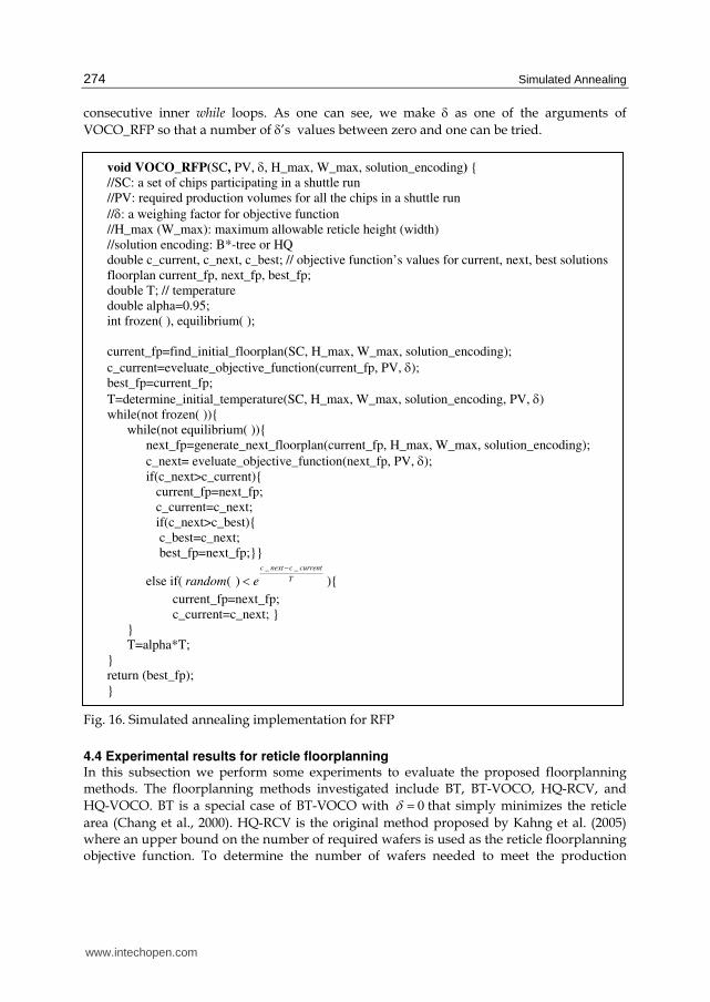
consecutive inner while loops. As one can see, we make δ as one of the arguments of
VOCO_RFP so that a number of δ’s values between zero and one can be tried.
Fig. 16. Simulated annealing implementation for RFP
4.4 Experimental results for reticle floorplanning In this subsection we perform some experiments to evaluate the proposed floorplanning methods. The floorplanning methods investigated include BT, BT-VOCO, HQ-RCV, and
HQ-VOCO. BT is a special case of BT-VOCO with 0δ = that simply minimizes the reticle
area (Chang et al., 2000). HQ-RCV is the original method proposed by Kahng et al. (2005) where an upper bound on the number of required wafers is used as the reticle floorplanning objective function. To determine the number of wafers needed to meet the production
void VOCO_RFP(SC, PV, δ, H_max, W_max, solution_encoding) {
//SC: a set of chips participating in a shuttle run
//PV: required production volumes for all the chips in a shuttle run
//δ: a weighing factor for objective function
//H_max (W_max): maximum allowable reticle height (width)
//solution encoding: B*-tree or HQ
double c_current, c_next, c_best; // objective function’s values for current, next, best solutions
floorplan current_fp, next_fp, best_fp;
double T; // temperature
double alpha=0.95;
int frozen( ), equilibrium( );
current_fp=find_initial_floorplan(SC, H_max, W_max, solution_encoding);
c_current=eveluate_objective_function(current_fp, PV, δ);
best_fp=current_fp;
T=determine_initial_temperature(SC, H_max, W_max, solution_encoding, PV, δ)
while(not frozen( )){
while(not equilibrium( )){
next_fp=generate_next_floorplan(current_fp, H_max, W_max, solution_encoding);
c_next= eveluate_objective_function(next_fp, PV, δ);
if(c_next>c_current){
current_fp=next_fp;
c_current=c_next;
if(c_next>c_best){
c_best=c_next;
best_fp=next_fp;}}
else if(_ _
( )c next c current
Trandom e
−< ){
current_fp=next_fp;
c_current=c_next; }
}
T=alpha*T;
}
return (best_fp);
}
www.intechopen.com
Reticle Floorplanning and Simulated Wafer Dicing for Multiple-project Wafers by Simulated Annealing
275
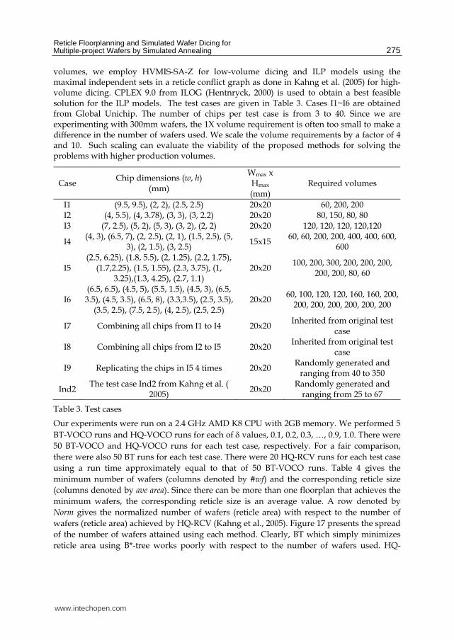
volumes, we employ HVMIS-SA-Z for low-volume dicing and ILP models using the maximal independent sets in a reticle conflict graph as done in Kahng et al. (2005) for high-volume dicing. CPLEX 9.0 from ILOG (Hentnryck, 2000) is used to obtain a best feasible solution for the ILP models. The test cases are given in Table 3. Cases I1~I6 are obtained from Global Unichip. The number of chips per test case is from 3 to 40. Since we are experimenting with 300mm wafers, the 1X volume requirement is often too small to make a difference in the number of wafers used. We scale the volume requirements by a factor of 4 and 10. Such scaling can evaluate the viability of the proposed methods for solving the problems with higher production volumes.
Case Chip dimensions (w, h)
(mm)
Wmax x Hmax
(mm) Required volumes
I1 (9.5, 9.5), (2, 2), (2.5, 2.5) 20x20 60, 200, 200 I2 (4, 5.5), (4, 3.78), (3, 3), (3, 2.2) 20x20 80, 150, 80, 80 I3 (7, 2.5), (5, 2), (5, 3), (3, 2), (2, 2) 20x20 120, 120, 120, 120,120
I4 (4, 3), (6.5, 7), (2, 2.5), (2, 1), (1.5, 2.5), (5,
3), (2, 1.5), (3, 2.5) 15x15
60, 60, 200, 200, 400, 400, 600, 600
I5 (2.5, 6.25), (1.8, 5.5), (2, 1.25), (2.2, 1.75),
(1.7,2.25), (1.5, 1.55), (2.3, 3.75), (1, 3.25),(1.3, 4.25), (2.7, 1.1)
20x20 100, 200, 300, 200, 200, 200,
200, 200, 80, 60
I6 (6.5, 6.5), (4.5, 5), (5.5, 1.5), (4.5, 3), (6.5, 3.5), (4.5, 3.5), (6.5, 8), (3.3,3.5), (2.5, 3.5),
(3.5, 2.5), (7.5, 2.5), (4, 2.5), (2.5, 2.5) 20x20
60, 100, 120, 120, 160, 160, 200, 200, 200, 200, 200, 200, 200
I7 Combining all chips from I1 to I4 20x20 Inherited from original test
case
I8 Combining all chips from I2 to I5 20x20 Inherited from original test
case
I9 Replicating the chips in I5 4 times 20x20 Randomly generated and
ranging from 40 to 350
Ind2 The test case Ind2 from Kahng et al. (
2005) 20x20
Randomly generated and ranging from 25 to 67
Table 3. Test cases
Our experiments were run on a 2.4 GHz AMD K8 CPU with 2GB memory. We performed 5
BT-VOCO runs and HQ-VOCO runs for each of δ values, 0.1, 0.2, 0.3, …, 0.9, 1.0. There were
50 BT-VOCO and HQ-VOCO runs for each test case, respectively. For a fair comparison,
there were also 50 BT runs for each test case. There were 20 HQ-RCV runs for each test case
using a run time approximately equal to that of 50 BT-VOCO runs. Table 4 gives the
minimum number of wafers (columns denoted by #wf) and the corresponding reticle size
(columns denoted by ave area). Since there can be more than one floorplan that achieves the
minimum wafers, the corresponding reticle size is an average value. A row denoted by
Norm gives the normalized number of wafers (reticle area) with respect to the number of
wafers (reticle area) achieved by HQ-RCV (Kahng et al., 2005). Figure 17 presents the spread
of the number of wafers attained using each method. Clearly, BT which simply minimizes
reticle area using B*-tree works poorly with respect to the number of wafers used. HQ-
www.intechopen.com

Simulated Annealing
276
BT (Chang et al.,2000)
BT- VOCO HQ-RCV (Kahng et al. 2005)
HQ-VOCO Volume Case
#wf ave area #wf ave area #wf ave area #wf ave area
I1 1 114 1 136 1 139 1 138
I2 1 58 1 67 1 69 1 65
I3 1 53 1 67 1 124 1 94
I4 3 95 2 115 2 192 2 135
I5 2 62 2 106 2 146 2 115
I6 4 249 3 266 4 303 3 296
I7 7 305 4 333 6 371 4 352
I8 7 267 5 337 9 383 5 310
I9 10 244 7 288 10 352 6 308
Ind2 2 189 2 242 2 344 2 264
Total 38 1635 28 1956 38 2423 27 2077
1X
Norm 1 0.67 0.74 0.81 1 1 0.71 0.86
I1 4 114 3 138 3 138 3 138
I2 1 58 1 67 1 65 1 65
I3 1 53 1 66 2 111 1 87
I4 10 96 5 109 6 132 5 115
I5 4 61 4 72 4 79.2 3 67
I6 13 250 9 252 12 284 10 287
I7 24 305 16 333 23 360 15 340
I8 28 266 19 345 22 310 17 339
I9 29 244 21 266 27 354 22 281
Ind2 4 189 3 220 4 245 3 229
Total 118 1636 82 1867 104 2079 80 1948
4X
Norm 1.13 0.79 0.79 0.90 1 1 0.77 0.94
I1 9 114 6 138 6 138 6 138
I2 3 58 2 65 3 68 3 65
I3 2 53 2 53 4 98 2 92
I4 22 95 12 105 14 127 12 110
I5 9 61 7 65 9 86 8 72
I6 31 250 22 252 26 271 23 287
I7 57 305 38 314 53 351 37 340
I8 64 268 47 333 52 309 43 308
I9 63 244 50 266 57 298 52 306
Ind2 9 189 8 214 8 223 7 225
Total 269 1636 194 1804 232 1969 193 1944
10X
Norm 1.16 0.83 0.84 0.92 1 1 0.83 0.99
Table 4. Minimum number of wafers and the average reticle area (mm2)
VOCO (BT-VOCO) is 17%~29% (16%~26%) better than HQ-RCV. HQ-VOCO is about 1%~3% better than BT-VOCO. As one can see, BT-VOCO and HQ-VOCO were most viable approaches for minimizing the number of wafers. It is also interesting to see that the
www.intechopen.com
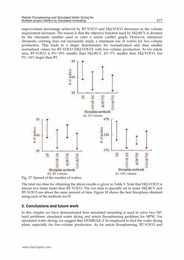
Reticle Floorplanning and Simulated Wafer Dicing for Multiple-project Wafers by Simulated Annealing
277
improvement percentage achieved by BT-VOCO and HQ-VOCO decreases as the volume requirement increases. The reason is that the objective function used by HQ-RCV is dictated by the chromatic number used to color a reticle conflict graph. However, minimum chromatic coloring does not necessarily imply a minimum use of wafers for low-volume production. This leads to a larger denominator for normalization and thus smaller normalized values for BT-VOCO (HQ-VOCO) with low-volume production. As for reticle area, BT-VOCO is 8%~19% smaller than HQ-RCV, 4%~7% smaller than HQ-VOCO, but 9%~14% larger than BT.
(a). 1X volume
(b). 4X volume
(c). 10X volume
Fig. 17. Spread of the number of wafers
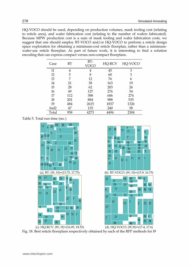
The total run time for obtaining the above results is given in Table 5. Note that HQ-VOCO is almost two times faster than BT-VOCO. The run time is specially set to make HQ-RCV and BT-VOCO use about the same amount of time. Figure 18 shows the best floorplans obtained using each of the methods for I9.
5. Conclusions and future work
In this chapter we have demonstrated how simulated annealing is used to solve two NP-hard problems: simulated wafer dicing and reticle floorplanning problems for MPW. For simulated wafer dicing, we suggest that HVMIS-SA-Z be employed to find the wafer dicing plans, especially for low-volume production. As for reticle floorplanning, BT-VOCO and
www.intechopen.com
Simulated Annealing
278
HQ-VOCO should be used, depending on production volumes, mask tooling cost (relating to reticle area), and wafer fabrication cost (relating to the number of wafers fabricated). Because MPW production cost is a sum of mask tooling and wafer fabrication costs, we suggest that one should employ BT-VOCO and/or HQ-VOCO to perform a reticle design space exploration for obtaining a minimum-cost reticle floorplan, rather than a minimum-wafer-use reticle floorplan. As part of future work, it is interesting to find a solution encoding that can express compact versus non-compact floorplans.
Case BT BT-
VOCO HQ-RCV HQ-VOCO
I1 4 4 45 3 I2 5 8 60 3 I3 7 12 76 6 I4 21 38 163 19 I5 28 62 203 26 I6 49 127 276 54 I7 112 388 606 274 I8 201 884 988 535 I9 484 2615 1837 1326
Ind2 47 135 240 58 Total 958 4273 4494 2304
Table 5. Total run time (sec.)
(a). BT: (W, H)=(13.75, 17.75)
(b). BT-VOCO: (W, H)=(15.9, 16.75)
(c). HQ-RCV: (W, H)=(16.05, 18.55)
(d). HQ-VOCO: (W,H)=(17.4, 17.6)
Fig. 18. Best reticle floorplans respectively obtained by each of the RFP methods for I9
www.intechopen.com
Reticle Floorplanning and Simulated Wafer Dicing for Multiple-project Wafers by Simulated Annealing
279
6. References
Andersson, M.; Gudmundsson, J. & Levcopoulos, C. (2005). Chips on wafer, Computational
Geometry - Theory and Applications, 30(2), 95-111
Bonn, J.; Sisler, S. & Tivnan, P. (2001). Balancing mask and lithography cost, Proceedings of
Advanced Semiconductor Manufacturing Conf., pp. 25-27
Chang, Y. C.; Chang, Y. W.; Wu, G. M. & Wu, S. W. (2000). B*-trees: a new representation for
non-slicing floorplans, Proceedings of ACM/IEEE Design Automation Conference, pp.
458-463
Chen, C. C. & Mak, W. K. (2006). A multi-technology-process reticle floorplanner and wafer
dicing planner for multi-project wafers, Proceedings of Asia and South Pacific Design
Automation Conference, pp. 777-782
Chen, S. & Lynn, E. C. (2003). Effective placement of chips on a shuttle mask, Proceedings of
SPIE. Vol. 5130, pp. 681-688
Ching, R. L. S. & Young, E. F. Y. (2006). Shuttle mask floorplanning with modified alpha-
restricted grid, Proceedings of ACM Great Lakes Symposium on VLSI, pp. 85-90
Global UniChip, http://www.globalunichip.com
Hentnryck, P. V. (2000). ILOG OPL Programming Language Reference Manual, Massachusetts
Institute of Technology
Kahng, A. B.; Mandoiu, I. I.; Wang, Q.; Xu, X. & Zelikovsky, A. (2004). Multi-project reticle
floorplanning and wafer dicing, Proceedings of International Symposium on Physical
Design, pp.70-77
Kahng, A. B. & Reda, S. (2004). Reticle floorplanning with guaranteed yield for multi-project
wafers, Proceedings of International Conference on Computer Design, pp. 106-110
Kahng, A. B.; Mandoiu, I. I.; Xu, X. & Zelikovsky, A. (2005). Yield-driven multi-project
reticle design and wafer dicing, Proceedings of 25th Annual BACUS Symposium on
Photomask Technology, pp. 1247-1257
Kirkpatrick, S.; Gelatt, C. D. & Vecchi, Jr. M. P. (1983). Optimization by simulated annealing,
Science, Vol. 220, No. 4598, May 13, pp. 671-680
LaPedus, M. (2006). Mask prices flatten but tool costs soar, EE TIMES, March 15
Lin, R. B.; Wu, M. C. & Tsai, S. C. (2007). Reticle design for minimizing multiproject wafer
production cost, IEEE Transactions on Automation Science and Engineering, Vol. 4, No.
4, pp. 589-595
Morse, R. D. (2003). Multiproject wafers: not just for million-dollar mask sets, Proceedings of
SPIE, Vol. 5043, pp. 100-113
Pina, C. A. (2001). MOSIS: IC prototyping and low volume production service, Proceedings of
Intl. Conf. on Microelectronic Systems Education, pp. 4-5
Pramanik, D.; Kamberian, H.; Progler, C.; Sanie, M. & Pinto, D. (2003). Cost effective
strategies for ASIC masks, Proceedings of SPIE, Vol. 5043, pp. 142-152
Tian, R.; Wong, D. F. & Boone, R. (2001). Model-based dummy feature placement for oxide
chemical–mechanical polishing manufacturability, IEEE Trans. Computer-Aided
Design, Vol. 20, No. 7. pp. 902–910
Wong, D. F. & Liu, C. L. (1986). A new algorithm for floorplan design, Proceedings of
ACM/IEEE Design Automation Conference, pp. 101–107
www.intechopen.com
Simulated Annealing
280
Wong, D. F.; Leong, H. W. & Liu, C. L. (1988). Simulated Annealing for VLSI Design, Kluwer
Academic Publishers
Wu, M. C. & Lin, R. B. (2005). Reticle floorplanning of flexible chips for multi-project wafers,
Proceedings of IEEE/ACM Great Lake Symposium on VLSI, pp. 494-497
Wu, M. C.; Tsai, S. C. & Lin, R. B. (2006). Floorplanning multiple reticles for multi-project
wafers, Proceedings of International Symposium on VLSI Design, Automation, and Test,
pp. 143-146
Wu, M. C. & Lin, R. B. (2008). Finding dicing plans for multiple project wafers fabricated
with shuttle mask, Journal of Circuits, Systems, and Computers, Vol. 17, No. 1, pp. 15-
31
Wu, M. C.; Lin, R. B. & Tsai, S. C. (2008). Chip placement in a reticle for multiple project
wafer fabrication, ACM Transactions on Design Automation of Electronic Systems, Vol.
13, No. 1
Xu, G.; Tian, R.; Wong, D. F., & Reich, A. J. (2003). Shuttle mask floorplanning, Proceedings of
SPIE, Vol. 5256, pp. 185-194
Xu, G.; Tian, R.; Pan, D. Z. & Wong, D. F. (2004). A multi-objective floorplanner for shuttle
mask optimization, Proceedings of SPIE, Vol. 5567, pp. 340-350
Xu, G.; Tian, R.; Pan, D. Z. & Wong, D. F. (2005). CMP aware shuttle mask floorplanning,
Proceedings of Asia and South Pacific Design Automation Conference, pp. 1111-1114
www.intechopen.com

Simulated AnnealingEdited by Cher Ming Tan
ISBN 978-953-7619-07-7Hard cover, 420 pagesPublisher InTechPublished online 01, September, 2008Published in print edition September, 2008
InTech EuropeUniversity Campus STeP Ri Slavka Krautzeka 83/A 51000 Rijeka, Croatia Phone: +385 (51) 770 447 Fax: +385 (51) 686 166www.intechopen.com
InTech ChinaUnit 405, Office Block, Hotel Equatorial Shanghai No.65, Yan An Road (West), Shanghai, 200040, China
Phone: +86-21-62489820 Fax: +86-21-62489821
This book provides the readers with the knowledge of Simulated Annealing and its vast applications in thevarious branches of engineering. We encourage readers to explore the application of Simulated Annealing intheir work for the task of optimization.
How to referenceIn order to correctly reference this scholarly work, feel free to copy and paste the following:
Rung-Bin Lin, Meng-Chiou Wu and Shih-Cheng Tsai (2008). Reticle Floorplanning and Simulated Wafer Dicingfor Multiple-Project Wafers by Simulated Annealing, Simulated Annealing, Cher Ming Tan (Ed.), ISBN: 978-953-7619-07-7, InTech, Available from:http://www.intechopen.com/books/simulated_annealing/reticle_floorplanning_and_simulated_wafer_dicing_for_multiple-project_wafers_by_simulated_annealing