Embed Size (px)
Citation preview

Resonant Tunneling Diodes:Models and Properties
JIAN PING SUN, GEORGE I. HADDAD,LIFE FELLOW, IEEE,PINAKI MAZUMDER, SENIOR MEMBER, IEEE, AND JOEL N. SCHULMAN
The resonant tunneling diode (RTD) has been widely studiedbecause of its importance in the field of nanoelectronic scienceand technology and its potential applications in very highspeed/functionality devices and circuits. Even though muchprogress has been made in this regard, additional work is neededto realize the full potential of RTD’s. As research on RTD’scontinues, we will try in this tutorial review to provide thereader with an overall and succinct picture of where we standin this exciting field of research and to address the followingquestions: What makes RTD’s so attractive? To what extentcan RTD’s be modeled for design purposes? What are therequired and achievable device properties in terms of digitallogic applications? To address these issues, we review the deviceoperational principles, various modeling approaches, and majordevice properties. Comparisons among the various RTD physicalmodels and major features of RTD’s, resonant interband tunnelingdiodes, and Esaki tunnel diodes are presented. The tutorial andanalysis provided in this paper may help the reader in becomingfamiliar with current research efforts, as well as to examinethe important aspects in further RTD developments and theircircuit applications.
Keywords—Nanoelectronics, quantum theory, quantum wells,resonant tunneling devices, semiconductor device modeling.
I. INTRODUCTION
Over the past two decades, resonant tunneling diodes(RTD’s) have received a great deal of attention followingthe pioneering work by Esaki and Tsu [1]. Significantaccomplishments have been achieved in terms of RTDdevice physics, modeling, fabrication technology, and cir-cuit design and applications. The RTD has been widelystudied, and well over a thousand research papers have beenwritten on various aspects of this seemingly simple device.Yet, whether RTD’s will find their way into mainstream
Manuscript received March 11, 1997; revised December 22, 1997. Thiswork was supported by the ARO-URI program under Grant DAAL03-92-G-0109.
J. P. Sun, G. I. Haddad, and P. Mazumder are with the Center forHigh Frequency Microelectronics, Solid State Electronics Laboratory,Department of Electrical Engineering and Computer Science, Universityof Michigan, Ann Arbor, MI 48109-2122 USA.
J. N. Schulman was with the Center for Collaborative Research,University of Tokyo, Tokyo, Japan. He is now with HRL Laboratories,Malibu, CA 90265 USA.
Publisher Item Identifier S 0018-9219(98)02492-X.
electronics in the future remains inconclusive. The researchis ongoing and, in some areas, very active. Why has thisdevice, typically consisting of two potential barriers andone quantum well, been so attractive to the electronicsresearch community for such a long period? With allthe knowledge about RTD’s so far acquired, will RTD’sbecome practical? What are the main issues of currentresearch on RTD’s? To get at these questions, we presentin this tutorial review an updated and succinct picture thataddresses some important aspects of RTD’s. For formaltreatments and detailed analysis on specific topics of RTD’s,the interested reader can find a number of excellent papers,review articles, and books, which will be referred to in therelevant context. This paper will cover the device aspects,while the circuit aspects on RTD circuit design and digitalapplications will be reviewed in an accompanying paper inthis issue [2].
It is well documented that today’s advanced informationtechnology is mainly attributed to the electronic represen-tation and processing of information in a low-cost, high-speed, very compact, and highly reliable fashion, and thatthe quest and accomplishments of continual miniaturizationand integration of solid-state electronics have been thekey to the success of the computer industry and computerapplications. The advanced multimedia infrastructure andservices in the future will demand further reduction inchip size. Chip density, represented by memory technology,has been following Moore’s law and has roughly doubledevery other year over the last three decades. The trendremains strong and definite, at least for the foreseeablefuture. For example, a 0.15-m process technology hasbeen implemented in the first 4-Gb dynamic random accessmemory (DRAM) unveiled in 1997, and the feature sizeof DRAM transistors is projected to be 0.18m (1 Gb)in 2001, 0.13 m (4 Gb) in 2004, 0.10 m (16 Gb) in2007, and 0.07 m (64 Gb) by 2010 [3]. A natural andrealistic question, then, is whether this desired trend willcontinue indefinitely. While an ultimate limit on the down-scaling of conventional transistors and integrated circuits(IC’s) will eventually be reached, device physicists and
0018–9219/98$10.00 1998 IEEE
PROCEEDINGS OF THE IEEE, VOL. 86, NO. 4, APRIL 1998 641

IC engineers have pondered answers, both evolutionaryand revolutionary, to the challenge. While the downscalingof conventional transistors enjoys an exceptional, rapidevolution, revolutionary device concepts have been activelysought, particularly in the two related areas known asnanoelectronics and single electronics [4]. For a more recentoverview of nanoelectronic devices, see [5].
The idea of nanoelectronics was popularized in the mid-1980’s, when pioneering work on resonant tunneling andbandgap engineering in low-dimensional semiconductorquantum wells and superlattices grew and was championedby several groups for the exploration of new opportunitiesfor circumventing the limit on the downscaling of con-ventional transistors and IC’s. The physics and electronicscommunities worldwide participated with enthusiastic re-search efforts, with rapid progress made in understandingmesoscopic transport physics as well as nanofabricationtechnology. The RTD, and its several variations, has be-come a research focus in nanoelectronics for its promise asa primary nanoelectronic device for both analog and digitalapplications.
It is well known that when the size of a system be-comes comparable to the electron wavelength, quantumeffects become dominant. This occurs when transistors aredownscaled and their characteristic dimensions reach thenanometer range, leading to new phenomena and possiblenovel devices based on quantum tunneling mechanisms. Fornanoelectronics to become a reality, it is essential that thenew devices and circuits must be fabricated with nanometerprecision, and one must be able accurately to design thedevices and circuits. This has led to research efforts andaccomplishments in three areas: nanofabrication, quantummodeling, and circuit innovations.
For device realization, nanofabrication technology hasmade impressive advances during the last decade by rou-tinely producing artificial semiconductor structures usingmolecular-beam epitaxy, metal-organic chemical vapor de-position, and chemical-beam epitaxy. Accurately controlledfeature sizes as small as monolayers of atoms in thegrowth direction for dissimilar semiconductor materials,or heterostructure systems, have been achieved. Nanoscalelithography and patterning by electron-beam lithographyhave also been highly developed in the direction perpendic-ular to the growth direction. Although further improvementsin this area call for more precise control, better resolution,and improved interfaces, recent advances in nanofabricationtechnology have brought quantum effect device conceptsto reality and have presented a great challenge for devicephysicists in the theoretical analysis of nanoelectronic de-vices. For a recent review of nanofabrication, the reader isreferred to [6].
Continuing effort in quantum transport modelingof RTD’s is motivated by the need to understanddevice operation and to provide a primary test fordeveloping theoretical tools for nanoelectronic devices. Notsurprisingly, this is very different from traditional devicemodeling. Moreover, it provides valuable knowledge ofthe quantum aspects of electron transport in mesoscopic
systems. Since the useful device properties, e.g., fastswitching operation betweenON and OFF states, area consequence of the desired and controlled electronmotion in the device, it is essential for device designersto understand and quantify the transport processes.Based on physical models, one can adjust the structuralparameters and suppress the unwanted processes throughdevice design and optimization. For conventional devicessuch as metal–oxide–semiconductor (MOS) and bipolartransistors with feature sizes much larger than nanometers,semiclassical transport models have proven to be adequatefor successful device downscaling development. Thesedevice models become invalid in the nanometer regime,however, since the classical transport concepts treatelectrons (and holes) as particles, and the transportparameters are defined by taking ensemble averages ofthe particle motion. In nanostructures, a device theorythat can properly treat quantum transport phenomenabetween macroscopic and microscopic scales is thereforeneeded. Work in this field has invoked mesoscopic physicalprinciples and hierarchical quantum device models forformulating and quantifying nanoelectronic transport anddevice analysis. However, the available nanoelectronicdevice models have not been well established to thestandards of conventional device models. For example,it is still a formidable task to accurately predict the I–Vcharacteristics of nanoelectronic devices, such as RTD’s.This topic is considered further in Section III.
Among the numerous nanoelectronic devices proposedand demonstrated, the RTD is perhaps the most promisingcandidate for digital circuit applications due to its nega-tive differential resistance (NDR) characteristic, structuralsimplicity, relative ease of fabrication, inherent high speed,flexible design freedom, and versatile circuit functionality.There is a good practical reason to believe that RTD’s maybe the next device based on quantum confined heterostruc-tures to make the transition from the world of research intopractical application. Progress in epitaxial growth has im-proved the peak-to-valley current ratio at room temperatureeven beyond that required for many circuit applications.This temperature requirement is the single most importantfeature that any new technology must satisfy. It is what dis-tinguishes the RTD from other interesting quantum deviceconcepts that have been proposed but that show weak, ifany, desired phenomena at room temperature. A variety ofcircuit functions has already been demonstrated, providingproof-of-concept of proposed applications [7]–[10]. Themain issue at present is not, in fact, the RTD perfor-mance itself but the monolithic integration of RTD’s withtransistors [high electron mobility transistors (HEMT’s) orheterojunction bipolar transistors (HBT’s)] into integratedcircuits with useful numbers and density of devices. Majorchallenges include the variation in the current–voltagecharacteristic of the RTD’s across a wafer and from waferto wafer, fabrication-dependent parasitic impedances, andedge effects as the RTD mesa area is decreased in orderto reduce the intrinsic parasitic impedances and to achievehigher integration levels. Recently developed techniques for
642 PROCEEDINGS OF THE IEEE, VOL. 86, NO. 4, APRIL 1998
Fig. 1. Physical processes in double-barrier tunneling.
providing feedback during epitaxial growth via optical andphotoemission probes have greatly improved the situationas far as uniformity of growth is concerned. It is for thesereasons that RTD research has been sustained for more thantwo decades and may now be rapidly approaching the stageof technology implementation. A more specific account ofRTD device features and properties as compared with otherNDR quantum devices is given in Section IV.
This paper is organized as follows. The resonant tun-neling phenomena is first reviewed in Section II, where asimple physical picture of the origin of the NDR is given fora basic understanding of RTD operation. Section III dealswith theoretical models of RTD’s. The hierarchical modelsof RTD’s with various levels of sophistication are com-pared and recent progress is summarized. Although RTDmodels have inspired intriguing physical and mathematicalformulations, it is not the purpose of this paper to go into adetailed treatment of quantum transport. Only the concep-tual framework and main features of various formalismsare examined, without engaging in details of the theory.For purposes of illustration, however, RTD operationalprinciples and modeling issues are exemplified using thesimple envelope function formulation. Section IV, on theanalysis of RTD properties, discusses the considerations fordesirable RTD characteristics for digital circuits and relatedissues in terms of carrier transport restrictions and realisticmaterial and structural considerations. The main features ofvarious RTD’s, resonant interband tunnel diodes (RITD’s),and Esaki TD’s are also compared and summarized. In thefinal section, concluding remarks are given highlighting the
accomplishments and existing concerns in RTD research.This tutorial review on RTD issues cannot be encyclopedic,with an obvious omission of the high-frequency aspects ofRTD’s, but it is hoped that an overall picture of wherewe are with an updated account of this exciting researchfrontier is presented.
II. RESONANT TUNNELING
A. Double-Barrier Quantum Well (DBQW) Structure
The basic RTD device configuration is a DBQW struc-ture of nanometer dimensions, including two contacts asdepicted in Fig. 1, where the regions I, II and VI, VIIare heavily doped contacts made from a semiconductorwith a relatively small bandgap, e.g., GaAs. These layerscomprise the emitter and collector, respectively. RegionsIII and V are quantum barriers made from a semiconductorwith a relatively larger bandgap, e.g., AlGaAs, and inparticular a positive conduction-band offset with respectto the smaller bandgap semiconductor. Region IV betweenthe two barriers is the quantum well made again fromthe smaller bandgap semiconductor. It is sometimes alsocalled the base, whether or not electrical contact is actuallybeing attempted. The structure is shown in terms of electronenergy versus distance under bias because we are interestedin the electron transport process, which is essentially theelectron motion within a certain energy-band structureunder applied bias voltages. Because the characteristicdimensions of the DBQW structure are comparable with theelectron wavelengths, the wave nature of electrons leads to
SUN et al.: RTD’S: MODELS AND PROPERTIES 643

quantum phenomena such as interference, tunneling, energyquantization, etc. As a result, resonant tunneling phenomenaoccur in DBQW structures and form the basis for RTDoperation.
The basic RTD structure shown in Fig. 1 may have manyvariations in terms of the potential (energy) profile, whichis determined primarily by the specific material systemused. We will consider issues of the material system anddevice structure in Section IV when we discuss deviceproperties. Fig. 1 gives a descriptive picture of the majorphysical processes pertaining to resonant tunneling andcurrent transport components in RTD’s.
B. Physical Processes in RTD’s
Envision a spectrum of electrons in region I, driven bya bias voltage applied across the RTD contacts, incidentupon the DBQW structure shown in Fig. 1. The electronspectrum is considered to be distributed in energy accordingto the Fermi–Dirac statistics as the contacts are typicallyheavily doped to provide a low ohmic contact and highcurrent density. The use of the Fermi distribution impliesthat the electrons in region I are assumed in thermalequilibrium due to the interactions among the electrons andtheir surroundings in contact region I. The same assumptionis made for contact region VII. Electrons are also incidentfrom the right-hand-side contact region but are not shownin the figure; the current due to them is small under thebias condition as shown.
A first look at the RTD structure brings out the generalfeatures of the electron wave as it traverses the DBQW,resulting in the main characteristic of RTD’s, namely, theNDR. The electron undergoes multiple reflections fromthe interfaces due to its wave nature, leading to the reso-nant nature of the tunneling. Also, there are dimensionalchanges across the interfaces, i.e., the three-dimensional(3-D) density of states in the emitter versus the two-dimensional (2-D) density of states in the quantum well,as described in the next section. The multiple reflectionscause destructive or constructive interference dependingon the wavelength of the particular electron. For electronswith specific wavelengths that favor constructive interfer-ence, a near-unity transmission probability may be foundat energies corresponding to these wavelengths. In otherwords, resonant tunneling occurs at these resonant energylevels, which may have a finite width in energy due tobroadening mechanisms. This process is indicated in Fig. 1by process 1 for an electron with energy coincident withthe resonant energy . In addition to the transport throughthe resonant levels, other processes can also be identified.In process 2, an electron is first scattered into an energylevel in the emitter accumulation layer, which is a 2-Dpotential well in region II. It may then absorb a phonon andsequentially tunnel through the resonant level. Similarly,in process 3, an electron with an initial energy mayinteract with the lattice vibration by emitting a phonon,then tunnel through . On the other hand, electrons withsufficiently high energies (for example, ) may overcomethe barriers by thermionic emission, as indicated by process
4. Note that the incident electrons also have a finite, butsmall, probability to tunnel through the nonresonant energyranges that lie between the resonances. This current is animportant contribution to the valley current.
The physical processes involved in RTD operation are inactuality much more complex than the preceding simpledescription and are especially complicated by the elec-tron’s interaction with its environment. First of all, theelectrons have particle and energy exchanges with thebattery applying the bias voltage, which makes the deviceopen to the outside environment and very different froman isolated quantum system. Moreover, the electrons inthe RTD structure have interactions with lattice vibration,impurities, interface roughness, and alloy disorder, as wellas the interaction among themselves. In the wave pic-ture, an incident electron wave is scattered by not onlythe heterostructure potential profile but also the scatteringpotentials originating from these other scatterers. Theseprocesses may affect the device properties significantly,making an accurate physical model of realistic RTD’s aformidable task.
C. Origin of Negative Differential Resistance
An important feature of resonant tunneling is that elec-trons are incident from the 3-D contacts into the 2-Dquantum well, where the electrons have a plane-wave-like motion only in the and directions, as shown inFig. 1. We designate the in-plane wave vector or transverse
momentum . Following Luryi’s explanation[11], the conservation of the crystal transverse momentumof the tunneling electron is responsible for the NDR.
The electron energy in the 3-D emitter contact can bewritten as
(1)
where is the bottom of the conduction-band in theemitter in region I and the effective masses in the differentlayers are assumed to be the same at this point.
The electron energy in the quantum well is given by
(2)
where is the energy of an available th subbandin the quantum well. During tunneling, a reduction ofdimensionality occurs, but the tunneling electrons do notsee any potential change in the transverse directions andtheir transverse momentum is therefore conserved. Theelectron longitudinal momentum however, generallychanges with distance except in the flat band-edge regions.As ( ) is an accessible unoccupied state in thequantum well, from energy conservation one sees thattunneling is possible only for electrons with their momentain a disk with in the emitter Fermi sphere, where
. As the emitter–base potentialrises under bias, so does the number of electrons that cantunnel. For , which corresponds to ,
644 PROCEEDINGS OF THE IEEE, VOL. 86, NO. 4, APRIL 1998

the number of tunneling electrons per unit area reaches amaximum. When rises above , then at K,there are no electrons in the emitter that can tunnel into thequantum well while conserving their transverse momentum.The tunneling current density therefore has a sharp dropfrom its maximum value. Further increase of the bias and/ortemperature will further lift up the electron distribution inthe emitter, and electron thermionic emission and tunnelingthrough the top regions of the barriers will lead to anincrease in current density. It can then be appreciated thatthe origin of the NDR in the RTD characteristic requirestransverse momentum conservation as a condition.
III. RTD DEVICE MODELS
Formal treatment of the modeling of RTD’s entails ad-vanced quantum transport theory, possibly including ratherintricate formulations of multiband effective mass theory,quantum statistical theory based on the density matrix,Wigner functions, and Green’s functions. Frensley, Ferry,Grubin, and other authors have written extensive reviewpapers on related subjects, and interested readers can findmore detailed information from these reviews [12], [13].We present in this section an overview of various RTDmodels in a simplified conceptual framework of quantumtransport and a tabulated summary of the main features anddifferences of the models. The RTD’s dc I–V characteris-tic is taken as the primary example for illustrating RTDmodeling issues.
Significant effort has been devoted to developing physicalmodels of RTD’s with varying degrees of sophisticationand success. The interest in achieving an accurate RTDmodel lies in the fundamental motivation to gain insightinto mesoscopic transport and provide guidance for opti-mal device design, which are indispensable for conceivingnew devices and pursuing realistic device development.Moreover, we believe that there exists a lag in theo-retical modeling of quantum transport as compared tonanofabrication technology. Quantum device modeling hasyet to be as well established as modeling capabilitiesfor conventional MOS field-effect transistors (FET’s) andbipolar transistors. On the other hand, quantum transportproblems in nanoelectronic devices and their complicatedmaterial and structural dependence demand heavy relianceon computer simulation tools. In that sense, RTD modelsserve as a test vehicle for device modeling capabilities aswe progress into the nanoelectronic regime.
Device terminal properties are determined by studyingcarrier transport of the electrons, whose available energiesare described by the band structure. The carrier motionshould include the major physical processes, such as thosedepicted in Fig. 1, in a specific band profile. In order tocompute RTD I–V characteristics, it is clear that RTDmodeling should include two important aspects.
1) Proper energy-band parameters for a particular RTDstructure, built up from dissimilar materials and theirinterfaces. For example, the band offsets at the het-erointerfaces, carrier effective masses, and other ma-
Fig. 2. Elements of quantum device modeling.
terial parameters derived from the band structure mustbe available with accuracy.
2) A proper transport formalism, which must be able tomodel the major processes in the RTD. Since simplifi-cations, approximations, and numerical discretizationare always used in the various models, they mustnot violate the basic physical laws and principlesof quantum mechanics. However, in practice, thesesimplifications and approximations often compromisesome of these principles.
The general elements of quantum device models are out-lined in Fig. 2, which will be discussed in some detail.
From a first-principles point of view, the RTD as ananoelectronic device is in general an open quantum sys-tem, in which electron transport is three dimensional, timedependent, time irreversible, dissipative, and many-body in-teractive, with both particle and energy exchanges with thedevice’s environment. The device system is therefore verydifferent from a simple isolated quantum system, where aconservative Hamiltonian and the boundary conditions forthe Schrodinger equation may be readily formulated. Onthe other hand, since a full many-body formalism that iscomputationally manageable for such open device systemshas not been well established, and may not be necessary forcalculations of specific device properties, approximationsand simplifications are typically used in various modelingapproaches to simplify the calculations, provided that themajor transport processes can be properly modeled. Recentefforts in RTD modeling have generated fruitful results forevaluation of quantum effects in RTD’s and for devicedesign. In terms of the electron state description and the
SUN et al.: RTD’S: MODELS AND PROPERTIES 645
capability of correctly treating the electron interactionswith its environment, the existing RTD physical modelscan be classified into two categories: dynamic or coherentmodels and kinetic models. We first indicate their commoningredients before identifying their differences.
According to quantum mechanics, an electron can bedescribed by its quantum state, represented by its state func-tion. A simple or pure electron state is generally representedby the electron wave function and may be specified by itsamplitude, momentum (wave vector), energy, and phase;its time evolution follows the time-dependent Schrodingerequation. An interaction between an electron and an opticalphonon, however, may break the electron’s phase coherenceand generate correlations with other microparticles. We thenspeak of incoherent interactions and mixed electronic states.This is because the interacting particles have no phaserelation with the incident electron wave, and it is thereforein practice impossible to trace the variation of the electronwave function of every particle. According to quantum sta-tistical theory, the mixed state may be characterized by thedensity matrix, Wigner (distribution) functions, or Green’sfunctions. For device modeling purposes, we may have theview that common to all quantum transport models, onetakes amodel functionto represent electron states in aquantum device. Once the model function is evaluated fora specific device under specific operating conditions, otherphysical quantities of interest as well as device propertiescan all be calculated from the available model function. Itis the chosen model function that makes major differencesin terms of the formalism, capabilities, and results fromone model to another. The model function in the coherentdynamic models is typically the envelope function, whereasin the kinetic models, the density matrix, Wigner function,and Green’s functions are employed and formulated. Thesefunctions representing electron states in quantum devicesare capable of modeling, to varying degrees, the physicalprocesses in the device, such as electron transmission,reflection, and scattering processes, in a unified formulation.The central formulation in a model can be a single equationor a set of equations, depending on the chosen model. Sincethe approximations often render an approach inadequate forall the processes to be modeled even approximately, how-ever, additional formulation may still be needed. The centralequation is typically a nonlinear differential or differential-integral equation, and solutions to the equation requireextensive numerical work and computer programming aswell as significant computer resources.
An important issue closely related to the central equationsis boundary conditions. It is essential to have a propertreatment of boundary conditions for any device model. Itis especially critical for quantum device models where thedevice system is open to particle reservoirs and driven farfrom equilibrium. As restricted by the scope of this paper,however, we will only point out the boundary conditions inRTD models. For a comprehensive review on this topic, thereader is referred to an in-depth analysis by Frensley [12].
As in any physical system, one would like to find howa system evolves in time with a computable equation of
motion. Device transient and high-frequency properties,such as switching times and device admittance (impedance)at high frequencies, require a time-dependent solution of themodel function. For device dc I–V characteristics, solutionsof the time-independent or steady-state equation of themodel function often suffice. In this paper, we identify ineach approach acentral model equationassociated with itsmodel function. A solution for the model function leads tothe device terminal properties, such as I–V characteristics.
A. Envelope Function Models of RTD’s
RTD models based on the envelope function descriptionof electron states have been popular and very useful instudying RTD’s and other nanoelectronic devices becausethey are conceptually simple, computationally efficient, andcapable of modeling important properties of RTD’s. We willoutline RTD models based on the envelope function in thissection to illustrate the main issues.
The envelope function description for electron states insemiconductors has been well documented [14] and isfamiliar to device engineers. It is based on effective masstheory, where the internal crystal potential is integratedinto the effective response of carriers to an external ap-plied force, greatly simplifying the treatment of carriertransport in semiconductor devices. For RTD models, sincequantum phenomena must be included, the effective massSchrodinger equation is invoked to calculate the electronstate function, or the envelope wave function, neglecting therapidly varying periodic component. This is the first majorapproximation made in the envelope function formalism,which brings about a great simplification, at the price ofignoring the microscopic information of the central cell partof the true wave function. Another major approximationinvolved in the envelope function approach is that it islimited to pure state calculations, to be discussed shortly.
The time-independent effective mass Schrodinger equa-tion is the central equation of the envelope function model
(3)
where the potential term includes the device energy-band offset for the heterojunction, the bias voltage appliedacross the device, the contributions from the doping im-purities, and mobile electronic charge. These enterin a mean-field, self-consistent fashion (the Hartree poten-tial) through the coupling of (3) with Poisson’s equation.Additionally, the electron correlation and exchange po-tential due to the interaction of electrons may also beincluded. The effective mass is specified accordingto the corresponding materials. The subscriptindicatesthe th band, indicates the electron wave vector, andindicates the position vector. Equation (3) is often convertedin practice into a one-dimensional (1-D) calculation usinga weighting function , also known as the supplyfunction for incident electrons, which effectively integratesover transverse wave vectors. The Schrodinger equation
646 PROCEEDINGS OF THE IEEE, VOL. 86, NO. 4, APRIL 1998

Table 1 Features of Various RTD Models
is then specified for a particular device structure and biascondition, and various numerical methods and algorithmsare used for the solution of the electronic wave functions.The boundary conditions of the Schrodinger equation andthe normalization of the wave functions are critical forobtaining the correct solutions. The boundary conditionsused in the envelope function model and other quantumdevice models will be listed in Table 1 and discussed brieflywhen RTD quantum models are summarized.
In the envelope function model, electronic conductionin quantum systems is represented by the transmissioncoefficient based on the Landauer and Buttiker [15], [16]formulation. The transmission , as a function of thelongitudinal electron energy, is the probability ratio of theincident and transmitted waves of a particular electron state,which is equivalent to the ratio of incident and reflectedelectron flux if the ratio of group velocities is also included.
To model the I–V characteristic of the RTD, a spectrumof electron eigenstates are taken to be incident from thecontacts, and the electron waves are then subject to elasticand inelastic scattering by various scattering potentials in-cluded in the formulation of . The electron eigenstatesin the contacts are assumed to be plane waves, and thereflected and transmitted wave functions are solutions ofthe Schrodinger equation for the specified RTD potentialprofile, including the scattering potential terms and theeffective masses. Once the wave functions are found, thedevice current density can be computed
Im
(4)
where a superposition over suitably normalized quantumstates is performed. Equivalently, the current densitycan be evaluated using the Tsu–Esaki formula [17], and thetotal current density is obtained by summing the currentdensity of each state over occupied states multiplied bytheir transmission probability
(5)
where can be calculated from the wave functionsavailable in the solution of the Schr¨odinger equation andthe supply function obtained by integrating over hasbeen incorporated. Other symbols in (5) are conventional.
More recent RTD models using envelope functions haveincorporated additional important physical aspects such asspace charge effects, the 2-D accumulation layer in the RTDemitter region, multiband effects, and phonon scattering.These aspects are discussed next.
Space charge effects occur in RTD’s because of theimpurity doping profile and the mobile electronic chargethat exists in the quantum well(s) as well as in the emitternotch or accumulation region. Since the charge densityresponds to the same electrostatic potential it generates,one needs to solve for the self-consistent potential andcharge distributions. This is usually carried out by solvingPoisson’s equation and the effective mass Schrodingerequation iteratively, followed by the current density calcula-tion. Inclusion of self-consistency significantly modifies thedevice characteristics due to effects such as band bending,changes in the effective barrier height, the effective voltagedrop across the barrier, and the shifting of the resonantstate energies in the quantum well. Several versions ofthe self-consistent solution, with varying degrees of ap-proximation, now exist. Ohnishiet al. assume in theircalculation that thermal equilibrium is maintained outsidethe barriers while the injected electrons are transportedballistically through and between the barriers [18]. Cahayet al., however, assume quantum ballistic transport throughthe whole region between the contacts [19]. An importantchoice in such methods resides in which locations theinjected carriers are assumed to be maintained in thermalequilibrium, since it plays a critical role in the quantitativeresults for the quantum well charge and the current density.Which assumption is more appropriate may depend on thespecific device structure being modeled and the operatingconditions. More details on self-consistent calculations canbe found in the original work or in [20] and referencestherein.
One of the consequences of the self-consistent potentialis the formation of the 2-D accumulation layer in theRTD emitter region due to the band bending, in whichthe injected electrons can scatter into the quantized statesand then tunnel through the resonant energy levels with or
SUN et al.: RTD’S: MODELS AND PROPERTIES 647

without further scattering. This corresponds to process 2 inFig. 1. Current transport through the emitter accumulationlayer is important since it can change the device currentsignificantly. Within the envelope function model, Fiiget al.[21] have addressed this problem using an additional termin the emitter charge expression to account for the quantizedstates in the emitter accumulation layer, so that a quantumrepulsion effect is observed and the peak current evaluationincludes the contribution from carrier transport throughthese states. A better treatment of the emitter accumulationlayer is now incorporated in the kinetic model using Green’sfunctions. For details, see references to the Green’s functionmodel for RTD’s in Section III-B.
Multiband effects are important in RTD modeling be-cause in the envelope function description, the periodicpart of the true wave function is ignored or assumed tobe the same for different materials. In addition, if theinteraction of electrons in different bands is important forthe evaluation of the RTD current, a single-band effective-mass equation is not adequate. The most obvious problemwith single-band models is that they do not include bandnonparabolicity, which is due to the well-knownrepulsion of the light hole and conduction bands. Theenergy scale of the nonparabolicity effect is set by thebandgap and the energy difference between these twobands. Nonparabolicity in the conduction band implies thatthe effective mass increases as energy increases above theband minimum. This results in lower resonance energiesthan would otherwise be expected. The effect is especiallyimportant for RTD’s using small bandgap semiconductorssuch as the InGaAs in the very important InGaAs/AlAsdouble-barrier structure, which is lattice-matched to InP.As a result of these effects, the single-band models usuallypredict the second turn-on of the RTD I–V characteristic ata much higher applied bias voltage than experimental dataobtained in many RTD structures.
A second effect is more subtle but actually just as,or more, important. It is that the scale of the decay ofthe wave function in the barriers is also affected by thenonparabolicity. The simplest model that goes beyond thesingle-band model is Kane’s two-band model, derived fromthe theory [22]. Instead of the parabolic imaginary
relation within the bandgap of the barriersemiconductor, where is the magnitude of the imaginarywave vector, the energy dispersion can be approximated as
. Examination ofthis equation shows that this “imaginary” band links thelight hole and conduction-band extrema. Thus, at a givenenergy in the bandgap, is smaller than it would be inthe single-band model. Since the decay lengths are just
, they are significantly longer in the two-band model.Transmission, and thus currents, is exponentially dependenton the decay length. This can easily result in the single-bandmodel’s underestimating the current density by a factor oftwo or more for typical devices of interest. Furthermore,the single-band model is useless for the interband tunnelingdevices. For example, in the InAs/AlSb/GaSb RITD shown
Fig. 3. Schematic energy-band-edge diagram of anInAs/AlSb/GaSb RITD.
in Fig. 3, the electron is incoming in the InAs conductionband. The band alignment is such that the valence bandof GaSb lies above the conduction band of InAs. Thus,that same electronic wave function is hole-like in the GaSbregion. The two-band model is the simplest frameworkfor incorporating this kind of situation, as it includes oneconduction band and one valence (light hole) band in eachmaterial.
To incorporate multiband effects, Schulman introducedthe two-band model into RTD modeling [23]; Rousseauet al. incorporated the multiband tight-binding model forRTD’s [24], which was then further improved by severalauthors. For example, the ten-band nearest neighbormodel [25] has been extended very recently to give im-proved material parameters and modeling results of RTDI–V characteristics by Boykin [26] and Bowenet al. [27].
Within the effective mass-envelope function framework,several formulations incorporating optical phonon scatter-ing processes have been attempted with varying degreesof success. Chevoiret al. [28] treat the incoherent currenttransport as a sequential process from an occupied emitterstate to a localized state in the well. Turleyet al. performedcalculations of resonant tunneling assisted by localizedphonons in double-barrier structures [29]. Roblinet al.[30] employ a multiple sequential scattering algorithm tocalculate scattering assisted tunneling currents. Caiet al.[31] use phonon annihilation and creation operators to formthe Hamiltonian of the electron–phonon interaction, and thisscheme was employed by Fuet al. [32] to calculate thephonon-assisted tunneling currents. In another approach,Stone et al. [33] and Zohta et al. [34] make use ofthe optical potential in analogy to its use in neutronscattering theory [35], in which an imaginary potential
is introduced into the Hamiltonian to treat thescattering problem. Based on their work, Sunet al. [36]have improved the model to obtain results in good agree-ment with the experiment. At present, however, no singleexisting envelope function model can accurately predictthe I–V characteristics for the whole range of RTD designparameters. A simple, elegant approach for the accuratedesign of I–V characteristics of realistic RTD structures isdesired but may not be feasible due to the fundamental
648 PROCEEDINGS OF THE IEEE, VOL. 86, NO. 4, APRIL 1998

Fig. 4. An envelope function model for RTD’s.
approximations used in this approach. Nonetheless, theenvelope function model for RTD’s and other quantumdevice structures is a valuable tool for simple deviceanalysis in the quantum regime.
For an illustration of an approximate treatment of in-elastic phonon scattering, a self-consistent RTD modelincluding the optical potential for optical phonon scatteringis described next in some detail. Its general procedure isoutlined in Fig. 4.
The effect of the imaginary potential on electron motioncan be seen directly from the time-dependent Schrodingerequation
(6)
where . Multiplying by on the left of (6)and taking the imaginary part, it follows that
(7)
where the electron density and current density aredefined, respectively, as
(8)
Im (9)
It is seen from (7) that in the steady state, the electroncurrent density is attenuated by the optical potential at arate of , which corresponds to a scattering time
. The simple form of the imaginary potential impliesthat the one-electron motion decays exponentially withtime. On the other hand, one can see that the probabilityof finding electrons in the quantum well is reducedcorresponding to an electron mean free path given by
, where is the electron velocity foran electron state and is the longitudinal electron energy.We have dropped the subscript. A damping constant forthe wave function in the quantum well can then be defined
accordingly
(10)
This allows us to express the electron wave function in thewell as a linear combination of damping wavesand for the solution of the Schr¨odinger equationwith the imaginary potential. This form for the wavefunction exhibits clearly that current conservation for theelectronic state is not preserved. This is fundamentally dueto the lack of unitarity of the Hamiltonian, which includesthe complex potential.
When applied to the phonon-assisted tunneling calcu-lation for RTD’s in the growth direction , the time-independent Schr¨odinger equation now becomes
(11)
where is now a variable electron effective mass, de-pending on the material composition of the individuallayers, and is the scattering rate of a hot electron in thequantum well that is derived using Fermi’s golden rule. Thevalue of can be approximated using the bulk scatteringrate for optical phonons.
For simplicity, and as a good approximation for hot elec-trons, the bulk scattering rate for optical phonon scatteringin the specific material is used similarly to typical MonteCarlo simulations
(12)
(13)
where is the resonant energy in the quantum welland is a prefactor of the scattering rates, adjustableto fit the experimental results. is the energy of theoptical phonon, is the Boltzmann constant, andis theabsolute temperature. If we designate to be the phononpopulation, or the Bose–Einstein factor in these equations,then (12) can be read as , representingthe case where both emission and absorption of the opticalphonon take place, whereas (13) becomes , whichis for the absorption case alone. The inelastic scatteringpotential is therefore energy dependent and related to thematerial used for the quantum well region in the RTD andto temperature.
In this approach, the total transmission is taken to bethe sum of the coherent transmission and incoherenttransmission . An attenuation coefficient is defined as
, where is the coherent reflectioncoefficient. After a single collision event, the attenuated partis assumed to tunnel in both the and directions inproportion to the transmission coefficient for each barrier,denoted respectively as for the right (the second) barrier
SUN et al.: RTD’S: MODELS AND PROPERTIES 649

Fig. 5. Modeled and measured RTD I–V characteristics using theenvelope function model with parameter adjustment.
and for the left (the first) barrier. Approximate analyticalexpressions have also been derived for these coefficients.To evaluate the transmission from regionto region , weuse the squared ratio of the transmitted electron flux to theincident flux
(14)
where is the transmitted wave amplitude, with as-sociated effective mass and wave vector , while
is the incident wave amplitude, with and inthe respective regions. The wave amplitudes are availablefrom the numerical solution to (11) for a particular self-consistent potential obtained using the procedureoutlined previously. The total transmission through thedouble-barrier structure is then
(15)
(16)
The total current density is evaluated according to (5) usingthe total transmission .
A comparison between calculated and measured RTDI–V characteristics is displayed in Fig. 5. Note, however,that good agreement between theory and experiment such asthis often involves parameter adjustment for the scatteringrate . Applying this approach to RTD’s with varyingdesign parameters is not as successful in obtaining goodagreement between modeled and measured results. In gen-eral, accurate prediction of RTD I–V characteristics cannotbe claimed. Moreover, as will be discussed next, there arefundamental limitations to the coherent model, especiallywhen a unified treatment of the electron and its interactionswith the surrounding microparticles is desired.
B. Kinetic RTD Models
The envelope function models are classified as dynamicmodels because they model the time-dependent or dy-namic device behavior based on the equation of motion ofthe system, i.e., the time-dependent Schrodinger equation.However, this framework cannot in principle treat the time-evolution of a system with internal force terms such asinelastic phonon scattering. For internal kinetics to beincluded, one has to invoke a kinetic equation such asthe Boltzmann transport equation, in which internal forcesare explicitly or implicitly incorporated. The pursuit ofquantum kinetic models of RTD’s was first motivated bythe desire for a correct treatment of the inelastic electron-phonon scattering process. The density matrix and Wignerfunction models were then developed with this goal inmind. A great deal of work has been performed on the ap-plication of Wigner functions to RTD modeling [37]–[40],and progress has generated very valuable information aboutRTD device properties. Although models based on theWigner function and the density matrix are based onestablished principles, however, phonon scattering in thesemodels is treated semiclassically within the relaxation timeapproximation. The present authors’ experience is thatconsistent results for RTD I–V characteristics using theWigner function approach have not always been obtain-able over a range of device parameters when comparedwith experiment [41]. Very recently, the Green’s functionmodel has shown further improvement on the modeling ofphonon scattering and other electron interactions and hasgenerated encouraging results. It is currently under activedevelopment.
In this section, we describe and compare features ofkinetic models. Some degree of mathematical formalismis unavoidable in discussing this topic, but an attempt wasmade to make this section self-contained, and it may beskipped without sacrificing continuity.
In principle, the fundamental difference between thecoherent (or dynamic) and kinetic models is that the formeris based on the single-particle picture using the pure statedescription, while the latter is based on the many-particlepicture with mixed state description. Note, however, that inpractice, a kinetic RTD model can be reduced to the single-particle picture with the mixed state description retained,such as in the one-particle density matrix formulation. Be-cause of this fundamental difference, the coherent modelscannot treat interactions between the microparticles on arigorous basis. This difference can also be traced to thenature of the model function. In coherent models, theenvelope wave function is a one-particle, pure state wavefunction assumed to have phase coherence over the entiredevice, an interacting many-particle system. The phasecoherence is clearly not preserved for electrons experi-encing inelastic phonon scattering. For the same reason,the envelope function is not capable of properly modelingelectron interactions in environments such as in the devicecontacts, where energy and particle exchanges take place.This is consistent with the central equation of the coherent
650 PROCEEDINGS OF THE IEEE, VOL. 86, NO. 4, APRIL 1998

Fig. 6. Electron current and wave function due to phonon scat-tering using the optical potential approach.
model. In the time-reversible effective mass Schrodingerequation for an electron state, the state does not change itseigenenergy during its time evolution. Accordingly, this is apure state description, which cannot treat electron–phononand electron–electron interactions if they are strong enoughsuch that the state energy changes and its phase coherence isdestroyed. This results in a mixed state. In the optical modelof optical phonon scattering within the envelope functionframework, the energy, particle, and current conservationprinciples do not hold, since there is no correlation betweenthe electron states being computed. This is deducible fromFig. 6, in that the electron wave function and the current aregreatly attenuated, but there is no correlation to include theeffect of this loss of current in one state to that of anotherin this framework.
When strong electron interactions must be included, onehas to go beyond simple, single-particle, pure quantumstates. Due to the statistical nature of quantum theory, adefinite, conserved Hamiltonian for the Schrodinger equa-tion for the system cannot be specified, and the electron canbe described in terms of a mixed state. In kinetic quantumtransport models, a quantum device is considered to bea particle ensemble, characterized by the density matrix,the Wigner (distribution) function, or Green’s functions.As a rigorous understanding of these model functionsinvolves advanced quantum physics concepts and extensiveformulation, we give here only a brief and superficialdiscussion to introduce the conceptual differences with thecoherent model and to identify the model functions and thecentral equations of these approaches.
First we separate the problem into two parts, i.e., thedevice under consideration and the environment outside thedevice. Then, let describe the device system in which we
are interested and let describe the part of the universeoutside the system. The density matrix is defined as
(17)
Its temporal evolution is given by the Liouville equation
(18)
where [ ] is the Poisson bracket and is the Liouvilleoperator. Equation (18) can be written in the followingform for device modeling
(19)
Based on Wigner’s definition, the Wigner function is theFourier transform of the one-particle density (matrix) op-erator
(20)
Alternatively, by performing the Wigner transformationfor the Schrodinger equation, one arrives at the Liouvilletransport equation, which gives the time evolution of theWigner function for device modeling
(21)
where the time derivative with subscript denotes a termdue to scattering and is the potential. In a simple form,the device is assumed to obey the Liouville equation
(22)
where is the collision operator
(23)and is the transition rate from to . Equation (22)expresses the time evolution of the Wigner function interms of the Liouville operator, representing the ballisticmotion, and a collision operator to include dissipativeinteractions such as the optical phonon scattering. The
SUN et al.: RTD’S: MODELS AND PROPERTIES 651
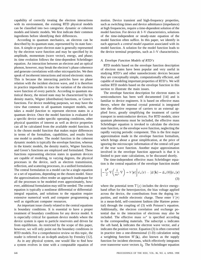
Fig. 7. Current density versus voltage for an RTD structure usingthe density matrix model. Reproduced from [42] with permission.
resultant quantum Liouville equation may be consideredas the quantum Boltzmann transport equation. In fact, inthe classical limit, (21) is reduced to the semi-classicalBoltzmann equation
(24)
where is the familiar Boltzmann distribution function.Conceptually, since the transport equation is written interms of a sum of many state functions, it is capableof describing mixed quantum states; the mixing of statesoccurs due to the scattering terms in (21). This kineticmodel offers a proper conceptual basis for dealing withquantum transport phenomena and has generated manyuseful insights into RTD physics and device properties.Fig. 7 shows an I–V curve modeled using the densitymatrix approach for a 200-nm RTD structure, with two5-nm, 300-meV barriers separated by a 5-nm well at 77K. More details of this work can be found in [42]. InFig. 8, a comparison between RTD I–V curves modeledby the (coherent) tunneling theory and by the Wignerfunction model is shown for a GaAs/AlGaAs RTD structureconsisting of a 4.5-nm quantum well bounded by 2.8-nm barriers. The scattering effects on the peak and valleycurrent densities in the Wigner function model are evident.For more details of comparison between these modelingresults, the reader is referred to the original paper [12].The major accomplishments, shortcomings, and detailedformulations of the density matrix and Wigner functionapproaches for RTD’s have been summarized in recentreviews [42], [43].
RTD models based on nonequilibrium Green’s func-tions have gained increasing interest recently because thisapproach offers a comprehensive physical basis for the
Fig. 8. Current density as a function of voltage for a model RTDusing the Wigner function model. Reproduced from [12] withpermission.
treatment of interactions between microparticles in thedevice system [44], [45]. Electron–electron interactions inthe contact regions, including the emitter accumulationlayer, electron–phonon interactions, and other scatteringprocesses, can also be readily incorporated in a unifiedformulation. This approach has produced improved resultsand more microscopic information in the device over theother RTD models [46].
Green’s functions are utilized to treat many physicalphenomena. For example, in electromagnetic theory, theyare used to calculate the response of a system to external,point excitations. More specifically, Green’s function de-termines the response in at time due to an excitationin at time . For transport problems such as in RTDmodeling, one takes the RTD current to be the responseto excitations. Nonequilibrium Green’s functions can beused, typically in matrix form, as a computational vehiclethat contains the information about device response tovarious excitations, such as applied voltage. Moreover,various scattering sources, such as phonons, electrons,impurities, interface roughness, etc., can be taken as internalexcitations, and the contributions to the current from theindividual excitations can then be calculated by summingup all the responses.
Several different but related nonequilibrium Green’sfunctions are required to encompass the increased micro-scopic information contained in the Green’s function modelfor RTD’s. The model functions consist of a number ofdifferent Green’s functions, i.e., the retarded and advancedGreen’s functions , , the correlation function ,and the self-energies . Heuristically, thesefunctions may be considered, respectively, as the electronwave response at different locations with respect to theexcitation, the correlation between different states atdifferent times, and the Hamiltonians of the scattering
652 PROCEEDINGS OF THE IEEE, VOL. 86, NO. 4, APRIL 1998
potentials. As the formalism needed to define and describethe Green’s functions correctly is nontrivial, we refer thereader to the description of Green’s functions in quantumphysics [47] and the treatment by Keldysh, Kadanoff, andBaym (the KKB formalism) [48], [49]. Datta has recentlywritten an excellent book explaining the use of Green’sfunctions for mesoscopic transport problems includingRTD calculations [50].
The central equation for the Green’s function approachcan be considered to be Dyson’s equation [51]. Startingfrom Dyson’s equation in the Keldysh formalism, Datta andLake formulated a set of equations for the Green’s functionsfor RTD steady-state transport calculations, which yield dcI–V characteristics [45], [52]. For example, the equationsfor the retarded Green’s function and the correlationfunction are
(25)
(26)
Other equations related to the self-energies are also neededfor the model but will not be listed here. Further approx-imations have also been used to simplify the formulationand numerical work.
RTD models based on nonequilibrium Green’s func-tions can include the electron–microparticle interaction ina unified framework. This gives more insight and micro-scopic information about the current transport, the effectsof inelastic scattering on the occupation of the energylevels, the density of states, the energy distribution ofthe current density, and the power density. These can allbe calculated for practical device structures under highbias conditions, which is not possible with other exist-ing RTD models. Recent efforts at Texas Instruments bythe Nanoelectronics Group, in collaboration with others,have produced nanoelectronic modeling (NEMO) softwareutilizing nonequilibrium Green’s functions to attempt state-of-the-art device modeling capabilities for RTD’s and toprovide a comprehensive quantum device modeling tool fornanoelectronic devices (see [46] by Klimecket al.). Thismodel includes the effects of quantum charging, band struc-ture, incoherent scattering from alloy disorder, interfaceroughness, ionized dopants, and acoustic and polar opticalphonons. The relevant publications have indicated that theNEMO program may be more accurate for modeling RTDI–V characteristics and other steady-state properties thanprevious RTD models. On the other hand, the develop-ment of KKB-based time-dependent modeling is still inits infancy. So far, only simplified transfer Hamiltonianshave been used [53], [54]. It is worth noting, however,that RTD’s are capable of operating in the terahertz fre-quency range, and time-dependent models may not bethat important for the frequencies of interest in the nearfuture for digital circuit applications being considered. In
addition, as is the case for other quantum kinetic devicemodeling, significant computer resources are demanded,both for memory and CPU time. Nonetheless, RTD modelsbased on nonequilibrium Green’s functions represent aremarkable advance in quantum transport modeling, andfurther enhancement of their capabilities is expected.
In Table 1, the major features of various RTD modelsdiscussed above are summarized to give a sketchy outlineof these models. Because we try to give a very simplifiedsummary in a tabulated form, some terms in the table areloosely used. For example, there, the Green’s functionsreally mean nonequilibrium Green’s functions. The densitymatrix model is categorized to be kinetic only in principle;it is not strictly true, however, for the RTD models basedon the one-particle density matrix formulation.
A brief discussion on the boundary conditions in RTDmodeling is in order. As alluded to in the beginning ofthis section, the boundary conditions must reflect the opennature of the device boundaries. Mathematically, valuesand derivatives of the model functions at the boundariesmay be formulated for the solution of the model equations.Listed in the table are the quantum transmitting boundarymethod (QTBM) proposed by Lent and Kirkner [55] andthe injected distribution function. The QTBM approachhas gained more applications recently. Generally speaking,the essence of this approach is to apply mixed boundaryconditions by fixing the values of linear combinationsof the model functions and their gradients at the deviceboundaries. The physical conditions at the boundaries andinterfaces can then be enforced during the entire solutionprocess. For a specific example of how it is implemented,see [56]. The injected distribution function approach isa traveling wave condition in that the boundaries emita quasicontinuum of eigenstate electrons with their wavevectors distributed according to the thermal equilibriumdistribution. The integral of these eigenstate electrons yieldsthe doping concentration at the contacts. One can appreciatethat this approach reflects the open nature of the devicecontacts and offers a proper formulation for the normaliza-tion of the model functions. Similar treatment of boundaryconditions is also applicable in RTD models based on theenvelope function approach.
In addition, we may note the difference between thenonequilibrium Green’s function model and the other ki-netic RTD models. In the entry of phonon scattering, underthe density matrix and Wigner function models, the relax-ation time approximation implemented in the collision termin these RTD models may also be characterized as beingMarkovian. The Markov approximation assumes that theevolution of the device system (through phonon scatteringin this context) does not depend upon its past history.This is reflected in the density matrix formulations, where
is a one-time model function. This assumption,however, is not made in the nonequilibrium Green’s func-tion model. Therefore, the Green’s function model has anadditional degree of freedom capable of modeling non-Markovian processes in the device. Further study of thispoint can be extended in relationships between the density
SUN et al.: RTD’S: MODELS AND PROPERTIES 653

matrix, Wigner function, and Green’s function formalisms.Treatment of other scattering processes included in theenvelope function and the Green’s function model can, inprinciple, be implemented in the density matrix and Wignerfunction models, but no report has been published to ourknowledge.
C. Other RTD Models
Based on the well-known Esaki–Tsu integral formula forthe tunneling current, many modifications and improve-ments have been made, such as the work by Coonet al.[57] and Changet al. [58]. Analytic models for the RTDcurrent such as those offer simple formulas relating the mostimportant physical ingredients of RTD operation but do notadequately predict experimental I–V behavior. On the otherhand, as RTD device and circuit developments advance tothe stage of practical circuit innovation and implementation,there is a need to bridge the gap between the available RTDphysical models and circuit simulation. The RTD quantummodels are too complicated and generally not accurateenough to be directly called from a circuit simulator. Recentattempts have begun to incorporate the RTD NDR intocircuit simulation models based on SPICE-type computer-aided design tools [59]. Therefore, simple analytic modelsthat closely relate both the essential RTD physical pa-rameters and measured I–V characteristics are desired.Work in this area follows analytical approximations forthe I–V characteristics based on transmission calculationswith adjustable empirical parameters linked as closely aspossible to real physical quantities. It has been shown thatsuch models can accurately reproduce experimental I–Vcharacteristics [60], which should be a very valuable toolfor realistic RTD device and circuit development.
There are several important issues to note when com-paring theoretical and experimental results, including theuncertainties in the material and doping profiles of thedevice, the possible error in the growth data, the materialparameters employed such as effective masses and bandoffsets, and the effects of imperfectly known parasiticimpedances on the measured I–V curve. These factorsmake it very difficult to obtain an accurate predictionor reproduction of experimental I–V characteristics anddemand more accurate characterization and calculation ofmaterial and structural parameters pertinent to RTD mod-eling calculations.
Last, there is a well-known issue that is conceptuallysimple but difficult to include in practice: the inclusion ofthe series and contact resistances. These resistances modifythe device I–V characteristics. It is difficult for all theabove models to include an accurate evaluation of theseresistances. Usually, a rough estimate or measurement ismade to fit the measured I–V curve, which may not besatisfactory for circuit designers if the RTD’s being usedhave a large fluctuation in their values for the resistance,and therefore in their peak and valley voltage values. Arecently proposed technique to determine the RTD I–Vcharacteristics experimentally based on microwave reflec-tion coefficient measurement may be useful in this regard
[61]. The importance of this issue will become clear in thenext section, where RTD I–V parameters for logic circuitsare discussed.
IV. DEVICE PROPERTIES
We now examine RTD dc properties, emphasizing onlythose that affect potential digital logic circuit applications,since this is where the major impact is expected. Beforespecific RTD dc properties required by its logic applicationsare discussed, we note that there are also serious consider-ations for analog applications, signal processing, and A/Dconverter applications of RTD’s, which are not covered inthis paper.
The most important property of an RTD lies in its NDR,which is sustainable to very high frequencies and offersvery fast switching speed. Of course, the time-dependentdevice properties possess interesting and subtle effects thathave absorbed a great deal of effort, particularly in relationto device transients and high-frequency behavior. Recentresults have shown that RTD’s can produce small amountsof power at frequencies above 800 GHz, and calculationspredict an NDR response in the terahertz range.
An analysis of RTD switching speed requires solving thecentral transport equations in the time domain. The resultingcurrent transient information can be Fourier transformedinto the frequency domain to obtain the admittance, whichcan in turn be used to construct a small signal circuitmodel for the analysis of the high-frequency properties.RTD switching characteristics have been investigated bymany authors. Liu and Sollner have recently written acomprehensive review covering many aspects of RTD high-frequency behavior (see [62] and references therein). De-spite the impressive high-frequency oscillations that havebeen demonstrated [63] and theoretical predictions that ter-ahertz frequencies are obtainable, current devices produceonly very low levels of output power and have limitedapplication as power sources. It is hoped that recentlyproposed schemes for coherently combining the power ofRTD’s in array form can overcome this limitation. We willnot discuss high-frequency aspects of RTD’s in this paper.
For realistic applications of RTD’s in digital circuits,some of the questions that need to be addressed are:What is required of the dc I–V characteristic for typicaldigital circuits, e.g., logic gates? How likely is it that theserequirements can be attained? What are the major issuesconcerning the choice of material system and structural con-siderations? In addition, there exist other quantum devices,notably the resonant tunneling transistor (RTT), the res-onant tunneling hot-electron transistor (RHET), the RITD,and the Esaki TD, all of which exhibit NDR characteristics.Is the RTD more attractive than the others? We will providea brief comparison among some of those devices in termsof their main features and properties. Before we make thecomparison, it is helpful to see what is required from thedevice NDR characteristics for digital logic applications.
First of all, it is important to note that two-terminal devicelogic circuits, i.e., using RTD’s alone, have several limita-
654 PROCEEDINGS OF THE IEEE, VOL. 86, NO. 4, APRIL 1998

Fig. 9. An example of logic gate consisting of RTD’s and HBT’s.
tions and are not adequate for most circuit applications.That is the main reason that circuits employing conven-tional Esaki TD’s did not materialize in the past. Recentadvances in very-high-frequency transistors such as HBT’sand HEMT’s, however, and the possibility of integratingNDR devices such as RTD’s with them, have changedthe picture significantly. The combination of these devicesnow holds great promise for very high speed/functionalitycircuits. In the next section, we will mainly consider anRTD-HBT-based circuit as an illustration [58], but certainlyRTD-HEMT based circuits and other circuits are also veryimportant and are being pursued.
A. NDR Characteristics and Parameters
For illustrating the issue of the integration of RTD’s andtransistors, we take a typical RTD-HBT threshold logic gateas an example. Fig. 9 shows the logic gate configurationwith HBT’s as the logic driver and an RTD usedas the load. This is referred to as a minority gate and canbe employed to achieve many digital functions. The logicgate operates as follows. The input currentsthroughchange to cause changes in the current flowing throughthe RTD load. When the clock (clk) signal goes high, itwill cause the total current through the RTD to increase.If more than inputs are high, the current through theRTD exceeds the peak current, causing a jump, and thusswitches the logic state to the second positive differentialresistance (PDR) region. This results in the node’sgoing low. If less than inputs are high, the currentthrough the RTD does not exceed the peak current and
remains high. When the clock signal goes low, theprevious output is maintained. When thereset line goeshigh, it will force all the transistors into cutoff. The currentflowing through the RTD will fall below the valley current,and the node is pulled high. When thereset linegoes back to zero, the node remains high. The logicoperation can also be seen from Fig. 10, which shows theintersections of the RTD’s I–V curve with the HBT’s I–V
Fig. 10. Intersecting characteristics of RTD’s and HBT’s in alogic gate.
characteristic. The I–V curve of the basic RTD devicecan be divided into three branches and six interrelatedNDR parameters as shown. There are two PDR branches,one before the peak point and one beyond the valleypoint, with the NDR region in between. Other importantquantities are the peak current (), peak voltage ( ),valley current ( ), valley voltage ( ), and the peak-to-valley current ratio (PVR). A voltage swing () maybe defined as the voltage at which the current reacheson the second PDR branch. Desired NDR characteristicscan be analyzed in terms of the above parameters. Therequirements on the RTD parameters can be consideredrelative to the noise margin, speed, and power dissipationfor the logic gate.
When the HBT’s are switched on by high (HI) inputsignals, the current flowing through the load RTD willintersect its PDR branch. If the current reaches, theoperating point will be switched to the point, producinga low output (LO) voltage, thus achieving a logic state.Conversely, a LO input signal at the HBT’s input will setthe RTD to a voltage near , the power supply of thegate. Since the noise margin of the logic gate is related tothe difference , we require and thus
to be as close to as possible. This demandsa low value for and high values for and .
The value sets up the logic relationship of the gatesince it determines the point at which the logic statechanges. However, it also depends on specific circuit driverconfigurations and therefore cannot be considered to be astringent requirement. Generally, too large a value of thepeak current is certainly undesirable from the viewpoint ofpower dissipation for future large-scale circuit integration.In addition, it takes time to reach a large peak current pointand then decrease to the valley point between the differentstates. This is undesirable for high speed. For the logiccircuit shown in Fig. 9, a value for of a fraction of amilliampere will usually suffice.
SUN et al.: RTD’S: MODELS AND PROPERTIES 655
Evaluating the valley current, and the related PVR,has been a major challenge, with the associated goals ofunderstanding current transport, improving RTD models,and achieving high PVR’s. In general, a low valley currentdensity is desired, as it is necessary for switching and isalso advantageous for low power consumption when large-scale RTD circuits are integrated. On the other hand, merelyseeking a very high PVR may be misleading and should beclarified. The PVR must be sufficiently large to provide thelogic function with a good noise margin, but it is not thesole figure of merit of an RTD. As can be seen in Fig. 10, ifthe PVR of the RTD is too low, a noise signal may triggerthe operating point near ( ) to move down along theNDR branch of the I–V curve, reaching the valley pointand then subsequently switching to an incorrect or faultystate. As a rule of thumb, a PVR of five would generallybe adequate; a value of ten is quite sufficient, and furtherpursuit of a much higher PVR may not be necessary forlogic applications.
It should be noted that the above discussion is an ex-ample for illustration. Since specific requirements for RTDcharacteristics may vary depending on the particular circuitconfiguration of different logic families and on differentdigital applications, the considerations may or may notapply for different digital circuits. For example, for RTD’sused for large-scale memory applications, the PVR will berequired to be as high as possible to reduce the standbypower consumption.
B. Material and Structural Considerations
The NDR characteristics considered in the precedingsection as representative device properties are a direct con-sequence of the carrier transport, described in Sections IIand III. They are closely related to the material system andspecific device structure. A great deal of research has beendevoted to exploring the various options for the realizationof optimum RTD’s.
It is obvious that for the sake of future large-scaleintegration, the most desirable material system would besilicon based, being compatible with current silicon ICtechnology. In contrast to the successful HBT performanceachieved in Si/SiGe heterosystems [64], however, attemptsat building RTD’s in the Si/SiGe system with acceptableI–V characteristics have not been encouraging, with PVR’snot much larger than one [65], [66]. The most importantrelevant parameter is the energy-band offset, particularlythe offset in the conduction band, because in most caseselectron transport is desired due to its lighter effectivemass as compared with holes. Although various schemesbased on the SiGe alloy band structures have been proposedand tested, the conduction-band offset between Si andSiGe alloys has been limited to a few of tenths of anelectron volt. This is not enough to produce the necessaryquantum confinement for a strong resonant state in theDBQW structure. Studies on hole resonant tunneling inSiGe systems have also been carried out [67], [68]. Tsu [69]has proposed silicon-based quantum wells with Si/SiOstrained layer superlattice barriers, but the structure has not
been demonstrated. This is probably due to difficulties inthe fabrication technology and strong electron scattering’sobscuring the resonance. Another possibility is to growmaterials with different bandgaps that are lattice matchedto silicon, for example, SiGeC materials [70]. There havealso been recent proposals for quantum MOS transistorsincorporating RTD’s, but a real breakthrough in this areais yet to come.
For RTD’s based on III–V compound ma-terials, the original traditional material system,GaAs(well)/AlGaAs(barrier), has been extended toGaAs/AlAs, InGaAs/AlAs, InGaAs/InAlAs, InAs/AlSb,and others. The work on RTD’s built from these materialsystems is extensive. For a summary of the various RTDcharacteristics achieved in these systems, see [71] bySeabaugh and Lake. RTD’s made from these systems canachieve a very high peak current density, a sufficient PVR,and a very high speed index (i.e., the ratio of the peakcurrent to the device capacitance).
At this time, the GaAs/GaAlAs and InGaAs/AlAs (on InPsubstrates) systems are the strongest candidates for actualcircuit insertion. The InGaAs/AlAs system is clearly supe-rior in terms of its intrinsic properties, but GaAs/GaAlAsIC fabrication technology is significantly more mature ingeneral. The focus now is onlow powerat moderately highfrequencies (tens of gigahertz), as there are other moreconventional high-frequency solutions available if poweris not the primary objective. In this regard, a variation ofthe InGaAs/AlAs system has come to the fore. It containsa modified InGaAs well with extra In inserted, either inthe form of a higher alloy concentration than called for bylattice matching or a small number of pure InAs centrallayers [72]. Either way, the extra In lowers the resonanceenergy in the well so that the peak voltage is loweredcorrespondingly. The tradeoff is that the peak currentdecreases as the resonance is lowered, so a compromiseis required. The lower voltage is absolutely essential if lowpower is to be achieved. For that purpose, an even bettersystem is the InAs/AlSb/GaSb RITD, or a variation thereof,which will be explained shortly.
While it may be straightforward in principle to controlthe peak current density by properly designing the DBQWstructure, it is not easy to realize this in practice. Thetunneling current density essentially has an exponentialdependence on the barrier thickness, which varies typicallyby one monolayer either way from the nominal thicknessaimed for in the epitaxial growth. The window for optimumcondition in the growth is narrow and often unforgiving,with no warrant of precise repetition. Therefore, iterativeadjustment is usually needed for a desired current density.Further, it is difficult to obtain the small values predictedby calculations for reasons related to device contact andseries resistances. The PVR is a combined result of thefactors relating to the valley current transport mechanisms,material system, structural design, and processing technol-ogy. The valley voltage naturally has material and structuraldependences that can be considered, as in Sections III andIV. Last, the swing voltage is related to the valley shape
656 PROCEEDINGS OF THE IEEE, VOL. 86, NO. 4, APRIL 1998

and the turn-on in the second PDR branch, which is verymuch related to the material parameters. For example, sincethe interaction between the conduction and valence-bandelectrons becomes more significant when the electric fieldstrength increases with applied voltage, an early turn-onand a small are expected for materials with a narrowerbandgap. In addition, it is easy to see that a low barriermaterial leads to earlier turn-on and a smaller voltageswing.
The above discussion indicates a strong dependence ofthe NDR on the material and structure. An initial designmay take these factors into consideration, but since factorsaffecting the resultant NDR and I–V characteristics arehighly nonlinear, modeling calculations to aid quantitativedesign are desirable. Previous material growth data andRTD processing parameters, if available, should be veryvaluable for a realistic assessment of expected RTD I–Vcharacteristics. Design and process iterations are often usedto obtain a desired device NDR characteristic.
In addition to the basic DBQW structure, several otherRTD structures have been investigated for interesting reso-nant tunneling physics, for possible performance improve-ment, and for a variety of potential applications. Notableexamples include polytype InAs/AlSb/GaSb RITD’s basedon resonant interband tunneling mechanisms [73]–[75], theSchottky-collector RTD’s [76], the double- and triple-wellRTD’s, which generate multiple NDR characteristics formultiple-valued logic circuits [77], [78], and, in yet anotherdirection, RTD’s of lower dimensions, so called 1-D andzero-dimensional (0-D) RTD’s [79], [80].
The main idea of an RITD is to combine interbandtunneling in Esaki TD’s and resonant tunneling in quantumwell structures. These combinations became possible due tovarious types of band lineups in polytype heterostructures.An example is shown in Fig. 3, where electrons tunnel fromthe conduction band (InAs contacts) through an interbandbarrier into light hole states in the valence band (GaSbquantum well). The peak current is caused by the tunnelingthrough a resonant state in the quantum well, as in the caseof conventional RTD’s. As the bias voltage passes reso-nance, however, the electrons will experience the bandgapnot only of AlSb but also of GaSb. Therefore, in principle,such devices are expected to have very high PVR’s, andthe published work has shown promising results. It mayhave a dramatically lower peak voltage but still with thehigh peak currents typical of InGaAs/AlAs without the extraIn. The low voltage is due to the Type II band alignment:the InAs emitter conduction-band edge proximity to theGaSb quantum well valence band. The positive mass ofthe conduction band relative to the negative valence-bandmass implies that there can be electrons satisfying theresonance condition even at very small biases. Fabricationof transistors in this material system has been demonstrated,but it is at a very early stage.
In a somewhat different version of RITD’s, heterostruc-ture p-n junction TD’s have also been demonstrated [81].For example, in an InGaAs/InAlGaAs/InGaAs tunnel diode,the wide-bandgap barrier layer is inserted in between the
two narrow-bandgap contact layers. The tunneling currentin such tunnel diodes is determined not only by the dopingprofile, as in a homojunction Esaki TD, but also by thebarrier width and height, which can be controlled to tune thedevice I–V characteristics, thus adding a degree of freedomin device design.
For Schottky-collector RTD’s, the ohmic-contacted col-lector of a conventional RTD is replaced with a directSchottky contact to the space charge layer near the secondbarrier, thereby eliminating the contact series resistanceon that side. This reduced series resistance leads to anincreased maximum frequency of oscillation. A 64-elementmonolithic Schottky-collector RTD oscillator array oscil-lated at 650 GHz has been reported [82].
In 1-D RTD’s, the electrons are laterally confined in theor directions using the convention of Fig. 1. Another
novel example is the variable-area RTD, in which thesize of the lateral confinement can be altered [83]. In0-D or quantum dot RTD’s, electrons are confined later-ally as well as vertically, but weakly coupled to electronreservoirs. Resonant tunneling has been observed in theselower dimensional RTD structures. These lower dimen-sional structures are interesting for studying the interplaybetween resonant tunneling and the Coulomb blockadeeffect in single electron structures [84]–[86]. These studiesmay produce interesting and promising device propertiesfor future electronics, but many practical difficulties due totheir extremely small size and increased complexity haveto be resolved.
C. Other NDR Quantum Devices
We now make a comparison between RTD’s and otherquantum devices with NDR characteristics. RTT’s andRHET’s, being three-terminal devices, have the advantagethat the NDR can be controlled by the voltage applied tothe third terminal, an attractive feature for circuit design,since it provides isolation between different circuit stages.This allows better control of device operation and gain.Although RTT operation has been demonstrated [87], it isextremely difficult to make a low resistive contact to theRTT base. On the other hand, RHET’s have limited gaindue to scattering in the base and are difficult to fabricate[88]. However, this controllable NDR characteristic can beobtained with RTD’s alone by connecting it in series withan FET or an HBT.
Another device whose operation is based on electrontunneling, the Esaki or tunnel diode, is the original quantumdevice with an NDR I–V curve. At that time, only discretedevices were possible. Now, there is no reason that theycannot also be integrated with HBT’s or HEMT’s. Thechallenges are different from those for RTD’s in that itis the doping that varies instead of the composition. One orthe other may be more appropriate for a given application.
Some of the important features of RTD’s, RITD’s, andEsaki TD’s that have been discussed are summarized inTable 2. A comprehensive comparison among these deviceswith an in-depth analysis is of current interest, and researchis ongoing on both device and circuit aspects.
SUN et al.: RTD’S: MODELS AND PROPERTIES 657

Table 2 Important Parameters of RTD’s, RITD’s, and TD’s. NoteThat at the Swing Voltage, the Device Current in the Second PDRRegion Reaches the Peak Current (See Also Fig. 10). The SpeedIndex Is the Ratio of the Peak Current over the Device Capacitance
V. CONCLUSIONS
It is generally agreed that the continued miniaturizationof transistors and IC’s may open a revolutionary regimefor novel semiconductor devices and circuits. Research innanoelectronics today stands at a frontier of semiconductorscience and engineering. The RTD is considered to bea major nanoelectronic device at the center of nanoelec-tronic research. In this review, we have addressed thefollowing questions. How well do we understand RTDdevice operation? How accurately are we able to modelits I–V characteristics and other properties? What basicrequirements are there for application in digital logic interms of the dc I–V characteristics? How realistic it isthat the desired I–V characteristics can be attained withavailable material and device structures? These issues werediscussed, and recent accomplishments as well as impedi-ments were reviewed.
Numerical modeling is playing an increasingly importantrole as a tool for gaining insight into nanoelectronic deviceoperation and providing guidance for device design. Quan-tum transport modeling and computer simulation tools willbe very valuable for conceiving new device concepts andexploring novel nanostructures. Sophisticated RTD modelshave been developed with varying levels of success in re-producing and predicting the I–V characteristics. Accuratepredictions of the I–V characteristics for different materialsystems and device structures are difficult to achieve. Thisis due to uncertainties in material growth and device processdata as well as in the material parameters, especiallywhen complicated materials and structures are involved.Therefore, more accurate characterization and calculationof material and structural parameters are needed for furtherdevelopment. We also note that RTD models, includingmultiband and scattering effects, can become quite com-putationally expensive and demand significant human and
computer resources, including a good understanding of ad-vanced quantum physics. Tradeoffs between modeling costand accuracy should be considered for specific applications.
RTD’s are very promising nanoelectronic devices fordigital logic circuit application due to their intrinsicallyhigh-speed NDR characteristics at room temperatures. In-tegrated circuits made from the III–V semiconductors arethe most likely opportunity for technology insertion, butif a material system compatible with silicon technologycould be achieved, the circuits could also be developedfor silicon very large scale integration. Another concernfor practical RTD applications is that achieving uniformityin resonant tunneling current, which depends exponentiallyon the parameters of the tunneling barriers, presents aserious challenge for circuit design and performance. How-ever, recent progress indicates thatin situ probing of theepitaxial growth, with real-time feedback into the growthprocess, may adequately achieve this goal. Nanoscience andnanotechnology are broad fields, highly interdisciplinary inbreadth and depth. It may take years for RTD’s to becomeroutine workhorses in future electronics. Whether or notRTD’s will achieve their promise may also be aided byadvances in other areas of quantum devices, such as singleelectronic devices and quantum MOS transistors now underactive research.
ACKNOWLEDGMENT
The authors wish to extend their sincere gratitude to manycolleagues for fruitful interactions. Special thanks are dueto Dr. H. Grubin of Scientific Research Associates, Dr. W.R. Frensley of the University of Texas at Dallas, Dr. D. K.Ferry of Arizona State University, Dr. G. Klimeck and Dr.R. Lake of Texas Instruments Incorporated, Dr. R. K. Mainsand Dr. J. R. East of the University of Michigan, and Dr.Y. Zohta of Tokyo Engineering University for their variouscontributions to this paper. They also wish to express theirtrue appreciation to the reviewers for their encouragementand constructive criticisms.
REFERENCES
[1] L. Esaki and R. Tsu, “Superlattics and negative differentialconductivity in semiconductors,”IBM J. Res. Develop.,vol. 14,pp. 61–65, Jan. 1970; R. Tsu and L. Esaki, “Tunneling in afinite superlattice,”Appl. Phys. Lett.,vol. 22, pp. 562–564, June1973; L. L. Chang, L. Esaki, and R. Tsu, “Resonant tunnelingin semiconductor double barriers,”Appl. Phys. Lett.,vol. 24,pp. 593–595, June 1974.
[2] P. Mazumder, S. Kulkarni, M. Bhattacharya, J. P. Sun, and G.I. Haddad, “Digital circuit applications of resonant tunnelingdevices,” this issue, pp. 664–686.
[3] T. Murotani, I. Naritake, T. Matano, T. Ohtsuki, N. Kasai, H.Koga, K. Koyama, K. Nakajima, H. Yamaguchi, H. Watanabe,and T. Okuda, “A 4-level storage 4Gb DRAM,” in1997 IEEEInt. Solid-State Circuits Conf. Dig.,San Francisco, CA, Feb.1997, p. 74; and H. Yasuda, “Multimedia impact on devices inthe 21st century,” in1997 IEEE Int. Solid-State Circuits Conf.Dig., San Francisco, CA, Feb. 1997, p. 28.
[4] D. V. Averin and K. K. Likharev, “Single electronics: A cor-related transfer of single electron and Cooper pairs in systemsof small tunnel junctions,” inMesoscopic Phenomena in Solids,B. L. Altshuler, P. A. Lee, and R. A. Webb, Eds. New York:North-Holland, 1991, ch. 6, pp. 173–271.
658 PROCEEDINGS OF THE IEEE, VOL. 86, NO. 4, APRIL 1998

[5] D. Goldhaber-Gordon, M. S. Montemerlo, J. C. Love, G.J. Optiteck, and J. Ellenbogen, “Overview of nanoelectronicdevices,”Proc. IEEE,vol. 85, pp. 521–540, Apr. 1997.
[6] D. A. Allee, A. N. Broers, and R. F. W. Pease, “Limits ofnano-gate fabrication,”Proc. IEEE, vol. 79, pp. 1093–1105,Aug. 1991; and H. Ahmed, “Nanostructure fabrication,”Proc.IEEE, vol. 79, pp. 1140–1148, Aug. 1991.
[7] H. Chan, S. Mohan, P. Mazumder, and G. I. Haddad, “Com-pact multiple-valued multiplexers using negative differentialresistance devices,”IEEE J. Solid-State Circuits,vol. 31, pp.1151–1156, Aug. 1996.
[8] J. van der Wagt, A. Seabaugh, and E. A. Beam III, “RTD/HFETlow standby power SRAM gain cell,” inIEDM 1996 TechnicalDigest. New York: IEEE Press, 1996, pp. 425–428.
[9] W. Williamson III, S. B. Enquist, D. H. Chow, H. L. Dunlap, S.Subramaniam, P. M. Lei, G. H. Bernstein, and B. K. Gilbert, “12GHz clocked operation of ultra-low power interband resonanttunneling diode pipelined logic gates,”IEEE J. Solid-StateCircuits, vol. 32, pp. 222–231, Feb. 1997.
[10] T. Waho, K. J. Chen, and M. Yamamoto, “Novel multiple-valued logic gate using resonant tunneling devices,”IEEEElectron Device Lett.,vol. 17, pp. 223–225, May 1996.
[11] S. Luryi, “Frequency limit of double barrier resonant tunnelingoscillators,”Appl. Phys. Lett.,vol. 47, pp. 490–492, Sept. 1985.
[12] W. R. Frensley, “Boundary conditions for open quantum sys-tems driven far from equilibrium,”Rev. Mod. Phys.,vol. 62,pp. 745–791, July 1990.
[13] D. K. Ferry and H. L. Grubin, “Modeling of quantum transportin semiconductor devices,” inSolid State Physics, Advancesin Research and Applications,vol. 49, H. Ehrenreich and F.Spaepen Eds. New York: Academic, 1995, pp. 283–448.
[14] M. Altarelli, “Band structure, impurities and excitons in super-lattices,” in Heterostructures and Semiconductor Superlattices,G. Allan and G. Bastard, Eds. Berlin: Springer-Verlag, 1996,pp. 12–37; and G. Bastard, J. A. Brum, and R. Ferreira,“Electron states in semiconductor heterostructures,” inSolidState Physics, Advances in Research and Applications,vol. 44,H. Ehrenreich and D. Turnbull, Eds. New York: Academic,1991, pp. 229–415.
[15] R. Landauer, “Electrical resistance of disordered one-dimensional lattices,”Philosophy Mag.,vol. 21, pp. 863–867,1970.
[16] M. Buttiker, Y. Imry, R. Landauer, and S. Pinhas, “Generalizedmany-channel conductance formula with applications to smallrings,” Phys. Rev. B.,vol. 31, pp. 6207–6215, May 1985.
[17] R. Tsu and L. Esaki, “Tunneling in a finite superlattice,”Appl.Phys. Lett.,vol. 22, pp. 562–564, June 1973.
[18] H. Ohnishi, T. Inata, S. Muto, N. Yokoyama, and A. Shibatomi,“Self-consistent analysis of resonant tunneling devices,”Appl.Phys. Lett.,vol. 49, pp. 1248–1250, Nov. 1986.
[19] M. Cahay, M. Mclennan, S. Datta, and M. S. Lundstrom,“Importance of space charge effects in resonant tunnelingdevices,”Appl. Phys. Lett.,vol. 50, pp. 612–614, Mar. 1987.
[20] J. P. Sun, R. K. Mains, W. L Chen, J. R. East, and G. I. Haddad,“C–V and I–V characteristics quantum well varactors,”J. Appl.Phys.,vol. 72, pp. 2340–2346, Sept. 1992.
[21] T. Fiig and A. P. Jauho, “Self-consistent model for two-dimensional accumulation layer states in resonant tunnelingdevices,”Appl. Phys. Lett.,vol. 59, pp. 2245–2247, Oct. 1991.
[22] E. O. Kane, “The k p method,” in Semiconductors andSemimetals, vol. 1, R. K. Willardson and A. C. Beer, Eds.New York: Academic, 1966, pp. 75–100.
[23] J. N. Schulman, “Ga1�xAlxAs–Ga1�yAlyAs–GaAs double-barrier structures,”J. Appl. Phys.,vol. 60, pp. 3954–3958, Dec.1986.
[24] K. V. Rousseau, K. L. Wang, and J. N. Schulman, “andstate influence on resonant tunneling current in single and
double barrier GaAs/AlAs structures,”Appl. Phys. Lett.,vol.54, pp. 1341–1343, Apr. 1989.
[25] P. Vogl, H. P. Hjalmarson, and J. D. Dow, “A semi-empiricaltight-binding theory of the electronic structure of semicon-ductors,” J. Phys. Chem. Solids,vol. 44, pp. 365–378, May1983.
[26] T. B. Boykin, “Incorporation of incompleteness in the kpperturbation theory,”Phys. Rev. B,vol. 52, pp. 16 317–16 320,Dec. 1995.
[27] R. C. Bowen, G. Klimeck, R. K. Lake, W. R. Frensley, and T.Moise, “Quantitative simulation of a resonant tunneling diode,”
J. Appl. Phys.,vol. 81, pp. 3207–3213, Apr. 1997.[28] F. Chevoir and B. Vinter, “Calculation of phononassisted tun-
neling and valley current in a double-barrier diode,”Appl. Phys.Lett., vol. 55, pp. 1859–1861, Oct. 1989.
[29] P. J. Turley and S. W. Teitsworth, “Theory of localized phononmodes and their effects ion electron tunneling in double barrierstructures,”J. Appl. Phys.,vol. 72, pp. 2356–2366, Sept. 1992.
[30] P. Roblin and W. R. Liou, “Three-dimensional scattering-assisted tunneling in resonant-tunneling diodes,”Phys. Rev. B,vol. 47, pp. 2146–2161, Jan. 1993.
[31] W. Cai, T. F. Zheng, P. Hu, B. Yudanin, and M. Lax, “Model ofphonon associated electron tunneling through a semiconductordouble barrier,”Phys. Rev. Lett.,vol. 63, pp. 418–421, July1989.
[32] Y. Fu, Q. Chen, and M. Willander, “Evanescent channels incalculation of phononassisted tunneling spectrum of a semi-conductor tunneling structure,”J. Appl. Phys.,vol. 74, pp.1848–1852, Feb. 1993.
[33] A. D. Stone and P. A. Lee, “Effect of inelastic processes onresonant tunneling in one dimension,”Phys. Rev. Lett.,vol. 54,pp. 1196–1199, Mar. 1985.
[34] Y. Zohta and T. Tanamoto, “Improved optical model for reso-nant tunneling diode,”J. Appl. Phys.,vol. 74, pp. 6996–6998,Dec. 1994.
[35] A. Bohr and B. Mottelson,Nuclear Structure, vol. 1. NewYork: Benjiamin, 1969.
[36] J. P. Sun and G. I. Haddad, “Self-consistent scattering calcu-lation of resonant tunneling diode characteristics,” presented atthe 1995 International Workshop for Computational Electronics,Tempe, AZ, Oct. 1995.
[37] W. R. Frensley, “Wigner function model of a resonant tunnelingdevice,” Phys. Rev. B,vol. 36, pp. 1570–1580, July 1987.
[38] R. K. Mains and G. I. Haddad, “Wigner function modeling ofresonant tunneling diodes with high peak-to-valley ratios,”J.Appl. Phys.,vol. 64, pp. 5041–5044, Nov. 1988.
[39] K. L. Jensen and F. A. Buot, “The effects of scattering oncurrent–voltage characteristics, transient response, and particletrajectories in the numerical simulation of resonant tunnelingdiodes,”J. Appl. Phys.,vol. 67, pp. 7602–7607, June 1990.
[40] N. C. Kluksdahl, A. M. Kriman, C. Ringhofer, and D. K. Ferry,“Quantum tunneling properties from a Wigner function study,”Solid-State Electron.,vol. 31, pp. 743–746. Mar./Apr. 1988.
[41] R. K. Mains and G. I. Haddad, “An accurate re-formulation ofthe Wigner function method for quantum transport modeling,”J. Comput. Phys.,vol. 112, pp. 149–161, May 1994.
[42] H. L. Grubin, “Density matrix simulations of semiconductordevices,” inQuantum Transport in Ultra-Small Devices,D. K.Ferry, H. L. Grubin, C. Jacoboni, and A. Jauho, Eds.,NATO ASISeries B: Physics. New York: Plenum, 1995, vol. 342, p. 241.
[43] F. A. Buot, “Mesoscopic physics and nanoelectronics:Nanoscience and nanotechnology,”Phys. Rep.,vol. 234, pp.73–174, Nov. 1993.
[44] E. V. Anda and F. Flores, “The role of inelastic scattering inresonant tunneling heterostructures,”J. Phys. Condens. Matter,vol. 3, pp. 9087–9101, Nov. 1991.
[45] R. Lake and S. Datta, “Nonequilibrium Green’s function methodapplied to double barrier resonant tunneling diodes,”Phys. Rev.B, vol. 45, pp. 6670–6685, Mar. 1992.
[46] G. Klimeck, R. Lake, R. C. Bowen, W. R. Frensley, and D.Blanks, “NanoElectronic MOdeling (NEMO),” in53rd AnnualDevice Research Conference Digest. New York: IEEE Press,1995, pp. 52–53; R. Lake, G. Klimeck, R. C. Bowen, C.Fernando, D. Jovanovic, D. Blanks, T. S. Moise, M. Leng,and W. R. Frensley, “Experimentally verified quantum de-vice simulations based on multiband models, Hartree self-consistency, and scattering assisted charging,” in54th AnnualDevice Research Conference Digest. New York: IEEE Press,1996, pp. 174–175.
[47] E. N. Economou,Green’s Functions in Quantum Physics,Springer Series in Solid-State Science, vol. 7. Berlin:Springer-Verlag, 1983.
[48] L. V. Keldysh, “Diagram technique for nonequilibrium pro-cesses,”Sov. Phys. JETP,vol. 20, pp. 1018–1026, Apr. 1965.
[49] L. P. Kadanoff and G. Baym,Quantum Statistical Mechanics.NY: Addison-Wesley, 1989.
[50] S. Datta,Electronic Transport in Mesoscopic Systems.Cam-bridge, U.K.: Cambridge Univ. Press, 1995.
[51] G. D. Mahan, “Quantum transport equation for electric and
SUN et al.: RTD’S: MODELS AND PROPERTIES 659

magnetic fields,”Phys. Rep.,vol. 145, pp. 251–318, Jan. 1987.[52] S. Datta, “Steady state quantum kinetic equation,”Phys. Rev.
B, vol. 40, pp. 5830–5833, Sept. 1989.[53] N. S. Wingreen, A. Jauho, and Y. Meir, “Time-dependent
transport through a mesoscopic structure,”Phys. Rev. B,vol.48, pp. 8487–8490, Sept. 1993.
[54] A. Jauho, N. S. Wingreen, and Y. Meir, “Time-dependenttransport in interacting and noninteracting resonant-tunnelingsystems,”Phys. Rev. B,vol. 50, pp. 5528–5544, Aug. 1994.
[55] C. S. Lent and D. J. Kirkner, “The quantum transmittingboundary method,”J. Appl. Phys.,vol. 67, pp. 6353–6359, May1990.
[56] J. P. Sun, R. K. Mains, K. Yang, and G. I. Haddad, “Aself-consistent model of- mixing in GaAs/AlAs/GaAs quan-tum well structures using the quantum transmitting boundarymethod,”J. Appl. Phys.,vol. 74, pp. 5053–5060, Oct. 1993.
[57] D. D. Coon and H. C. Liu, “Frequency limit of double barrierresonant tunneling oscillators,”Appl. Phys. Lett.,vol. 49, pp.94–96, July 1986.
[58] C. E. Chang, P. M. Asbeck, K. C. Wang, and E. R. Brown,“Analysis of heterojunction bipolar transistor/resonant tunnelingdiode logic for low-power and high-speed digital applications,”IEEE Trans. Electron Devices,vol. 40, pp. 685–691, Apr. 1993.
[59] S. Mohan, J. P. Sun, P. Mazumder, and G. I. Haddad, “Deviceand circuit simulation of quantum electronic devices,”IEEETrans. Computer-Aided Design,vol. 14, pp. 653–662, June1995.
[60] J. N. Schulman, H. J. De Los Santos, and D. H. Chow, “Physics-based RTD current-voltage equation,”IEEE Electron DeviceLett., vol. 17, pp. 220–222, May 1996.
[61] P. Huang, D. S. Pan, and N. C. Luhmann, Jr. “A microwavemeasurement technique for characterizing the I–V relationshipfor negative differential conductance devices,”IEEE Trans.Microwave Theory Tech.,vol. 41, pp. 1455–1458, Aug. 1993.
[62] H. C. Liu and T. C. L. G. Sollner, “High-frequency resonanttunneling diodes,” inSemiconductors and Semimetals,vol. 41,High-Speed Heterostructure Devices,R. A. Kiehl and T. C. L.G. Sollner, Eds. New York: Academic, 1994, pp. 359–419.
[63] E. R. Brown, J. R. Soderstrom, C. D. Parker, L. J. Mahoney,K. M. Molvar, and T. C. McGill, “Oscillation up to 712 GHzin InAs/AlSb resonant tunneling diodes,”Appl. Phys. Lett.,vol.58, pp. 2291–2293, May 1991.
[64] A. Gruhle, H. Kibbel, U. Erben, and E. Kasper, “91 GHz SiGeHBT’s grown by MBE,” Electron. Lett.,vol. 29, pp. 415–417,Feb. 1993.
[65] K. Ismail, B. S. Meyerson, and P. J. Wang, “Electron resonanttunneling in SiGe double barrier diodes,”Appl. Phys. Lett.,vol.59, pp. 973–975, Aug. 1991.
[66] U. Konig, M. Kuisl, J. F. Luy, and F. Schaffler, “Si/SiGe res-onant tunneling devices separated by surrounding polysilicon,”Electron. Lett.,vol. 26, pp. 1904–1906, 1990.
[67] H. C. Liu, D. Landheer, M. Buchanan, and D. C. Houghton,“Resonant tunneling in Si/Si1�x
Gex
double barrier structures,”Appl. Phys. Lett.,vol. 52, pp. 1809–1811, May 1988.
[68] U. Gennser, V. P. Kesan, S. S. Iyer, T. J. Bucelot, and E. S.Yang, “Resonant tunneling of holes through silicon barriers,”J.Vac. Sci. Technol.,vol. 8, pp. 210–213, Mar./Apr. 1990.
[69] R. Tsu, “Silicon-based quantum wells,”Nature,vol. 364, p. 19,July 1993.
[70] R. A. Soref, “Silicon-based optoelectronics,”Proc. IEEE,vol.81, pp. 1687–1706, Dec. 1993.
[71] A. Seabaugh and R. Lake, “Tunnel diodes,” inEncyclopedia ofApplied Physics, vol. 20. New York: VCH, 1996.
[72] T. Broekaert, W. Lee, and C. G. Fonstad, “PseudomorphicIn
:53Ga:47As/AlAs/InAs resonant tunneling diodes with peak-
to-valley ratios of 30 at room temperature,”Appl. Phys. Lett.,vol. 53, pp. 1545–1547, Oct. 1988.
[73] J. R. Soderstrom, D. H. Chow, and T. C. McGill, “New neg-ative differential resistance device based on resonant interbandtunneling,” Appl. Phys. Lett.,vol. 55, pp. 1094–1096, Sept.1989.
[74] L. F. Luo, B. Beresford, and W. I. Wang, “Interband tunneling inpolytype GaSb/AlSb/InAs heterostructures,”Appl. Phys. Lett.,vol. 55, pp. 2023–2025, Nov. 1989.
[75] M. Sweeny and J. M. Xu, “Resonant interband tunnel diodes,”Appl. Phys. Lett.,vol. 54, pp. 546–548, Feb. 1989.
[76] M. Reddy, M. J. Mondry, M. J. W. Rodwell, S. C. Martin, R.P. Smith, D. H. Chow, and J. N. Schulman, “Fabrication and
dc, microwave characteristics of submicron Schottky-collectorAlAs/In
:53Ga:47As/InP resonant tunneling diodes,”J. Appl.
Phys.,vol. 77, pp. 4819–4821, May 1995.[77] T. Nakagawa, H. Inamoto, T. Kojoima, and K. Ohta, “Ob-
servation of resonant tunneling in AlGaAs/GaAs triple barrierdiodes,”Appl. Phys. Lett.,vol. 49, pp. 73–75, July 1986.
[78] H. Mizuta, T. Tanoue, and S. Takahashi, “A new triple-wellresonant tunneling diode with controllable double-negativeresistance,”IEEE Trans. Electron Devices,vol. ED-35, pp.1951–1956, Nov. 1988.
[79] A. Kumar and P. H. Bagwell, “Resonant tunneling in aquasione-dimensional wire: Influence of evanescent modes,”Phys. Rev. B,vol. 43, pp. 9012–9020, Apr. 1991.
[80] M. A. Reed, J. N. Randall, R. J. Aggarwal, R. J. Matyi, T. M.Moore, and A. E. Westel, “Observation of discrete electronicstates in zero-dimensional semiconductor nanostructure,”Phys.Rev. Lett.,vol. 60, pp. 535–537, Feb. 1988.
[81] D. Day, Y. Chung, C. Webb, J. N. Eckstein, J. M. Xu, andM. Sweeny, “Heterostructure p-n junction tunnel diodes,”Appl.Phys. Lett.,vol. 57, pp. 1140–1142, Sept. 1990.
[82] M. Reddy, S. C. Martin, A. C. Molnar, R. E. Muller, R. P.Smith, P. H. Siegel, M. J. Mondry, M. J. W. Rodwell, and S. J.Allen, Jr., “Monolithic Schottky-collector resonant tunnel diodeoscillator arrays to 650 GHz,”IEEE Electron Device Lett.,vol.18, pp. 218–221, May 1997.
[83] C. J. Goodings, H. Mizuta, J. R. A. Cleaver, and H. Ahmed,“Variable-area resonant tunneling diodes using implanted in-plane gates,”J. Appl. Phys.,vol. 76, pp. 1276–1286, July 1994.
[84] M. Tewordt, L. Martin-Moreno, T. J. Nicholls, M. Pepper, M.J. Kelly, V. J. Law, D. A. Ritchie, J. E. F. Frost, and G. A. C.Jones, “Single electron tunneling and Coulomb charging effectsin asymmetric double-barrier resonant tunneling diodes,”Phys.Rev. B,vol. 45, pp. 14407–14410, June 1992.
[85] M. W. Dellow, C. J. G. M. Langerak, P. H. Beton, T. J. Foster,P. C. Main, L. Eaves, M. Henini, S. P. Beaumont, and C. D.W. Wilkinson, “Single electron tunneling through a donor statein a gated resonant tunneling device,”Surface Sci.,vol. 263,pp. 438–441, Feb. 1992.
[86] B. Su, V. J. Goldman, and J. E. Cunningham, “Single-electrontunneling in nanometer-scale double-barrier heterostructure de-vices,” Phys. Rev. B,vol. 46, pp. 7644–7655, Sept. 1992.
[87] G. I. Haddad, U. K. Reddy, J. P. Sun, and R. K. Mains, “Thebound-state resonant tunneling transistor (BSRTT): Fabrication,d.c. I–V characteristics, and high-frequency properties,”Su-perlattices and Microstructures,vol. 7, no. 4, pp. 369–374,1990.
[88] N. Yokoyama, H. Ohnishi, T. Futatsugi, S. Muto, T. Mori, K.Imamura, and A. Shibatomi, “Resonant-tunneling transistors us-ing InGaAs-based materials,”Proc. SPIE,vol. 943, pp. 14–21,Mar. 1988.
Jian Ping Sun received the B.S. degree fromNanjing Institute of Technology, China, and theM.S. and Ph.D. degrees from the University ofMichigan, Ann Arbor, all in electrical engineer-ing.
He was with the Nanjing Solid State DevicesResearch Institute, China, and the ElectronicsResearch Laboratories, University of Califor-nia at Berkeley. He is with the Solid StateElectronics Laboratory, Department of ElectricalEngineering and Computer Science, University
of Michigan, where he is an Assistant Research Scientist and VisitingAssistant Professor. His research interests include modeling and design ofhigh-speed, high-frequency semiconductor devices, quantum devices, andphotonic devices.
660 PROCEEDINGS OF THE IEEE, VOL. 86, NO. 4, APRIL 1998

George I. Haddad (Life Fellow, IEEE) re-ceived the B.S.E., M.S.E., and Ph.D. degreesin electrical engineering from the University ofMichigan, Ann Arbor.
In 1958, he joined the Electron Physics Labo-ratory, where he engaged in research on masers,parametric amplifiers, detectors, and electron-beam devices. From 1960 to 1969, he wassuccessively Instructor, Assistant Professor, As-sociate Professor, and Professor in the ElectricalEngineering Department of the University of
Michigan. In 1991, he was named the Robert J. Hiller Professor of Elec-trical Engineering. During 1975–1987 and 1988–1997, he was Chairmanof the Department of Electrical Engineering and Computer Science. Hecurrently is Director of the Center for High-Frequency Microelectronics.His current research areas are microwave and millimeter-wave solid-statedevices, monolithic integrated circuits, and microwave-optical interactions.
Dr. Haddad is a member of Eta Kappa Nu, Sigma Xi, Phi KappaPhi, Tau Beta Pi, and the American Society for Engineering Education.He was Editor of IEEE TRANSACTIONS ON MICROWAVE THEORY AND
TECHNIQUESfrom 1968 to 1971. He received the 1970 Curtis W. McGrawResearch Award from the American Society for Engineering Educationfor outstanding achievements by an engineering teacher, the College ofEngineering Excellence in Research Award (1985), the DistinguishedFaculty Achievement Award (1986), and the S. S. Atwood Award forexcellence in engineering research, education, and administration.
Pinaki Mazumder (Senior Member, IEEE) re-ceived the B.S.E.E. degree from the Indian In-stitute of Science in 1976, the M.Sc. degreein computer science from the University ofAlberta, Canada, in 1985, and the Ph.D. degreein electrical and computer engineering from theUniversity of Illinois at Urbana-Champaign in1987.
For two years, he was a Research Assistantwith the Coordinated Science Laboratory, Uni-versity of Illinois at Urbana-Champaign. For
more than six years, he was with Bharat Electronics, Ltd., India, where hedeveloped analog and digital integrated circuits for consumer electronicsproducts. During the summers of 1985 and 1986, he was a Member ofthe Technical Staff in the Naperville branch of AT&T Bell Laboratories.He presently is an Associate Professor with the Department of ElectricalEngineering and Computer Science, University of Michigan, Ann Arbor.His research interests include very-large-scale-integration testing, physicaldesign automation, ultrafast digital circuit design, and neural hardware.
Dr. Mazumder is a member of Sigma Xi, Phi Kappa Phi, and theAssociation of Computing Machinery Special Interest Group on DesignAutomation.
Joel N. Schulmanreceived the B.A. degree inphysics from the University of Pennsylvania,Philadelphia, in 1973 and the Ph.D. degree inphysics from the California Institute of Tech-nology, Pasadena, in 1979.
He is a Senior Research Scientist in the Sen-sors and Materials Laboratory of HRL Labora-tories, Malibu, CA, and an Adjunct Professorin the Department of Electrical Engineering atthe University of California, Los Angeles. Hisresearch interests include the electronic and op-
tical properties of semiconductor superlattices, quantum wells, and tunnelstructures.
SUN et al.: RTD’S: MODELS AND PROPERTIES 661