Embed Size (px)
Citation preview
F
ree
sca
le S
em
ico
nd
uc
tor,
In
c..
.
Order this documentby AN1744/D
AN1744
Resetting Microcontrollers During Power TransitionsBy Greg Racino
Consumer Systems GroupAustin, Texas
Introduction
A simple function such as resetting an MCU during the application orremoval of power can cause many problems if not handled properly.Symptoms of an improperly handled reset during power transitions canrange from a slight delay in MCU response after power-up to very erratic,inconsistent behavior to total system failure.
This document covers the main issues relating to this problem and aimsto lead the user of HC05, HC08, and HC11 devices to a safe and reliableapproach to transitioning power in their application.
Although the information in this application note applies to most HC05,HC08, and HC11 devices, some variations in the sources of reset andimplementation of the internal circuits do exist.
Consult the pertinent device specification in addition to this document tomake sure your system will operate properly during power transitions.
Motorola, Inc., 1998 AN1744
For More Information On This Product, Go to: www.freescale.com
Application Note
F
ree
sca
le S
em
ico
nd
uc
tor,
I
Freescale Semiconductor, Inc.n
c..
.
Document Outline
Reset in its most basic function ensures that the MCU starts or restartsexecuting software code in a controlled manner. This document coversthose situations that are related to resetting the MCU when power isapplied and removed from the MCU. It does not cover general systemprotection features such as COP (computer operating properly), illegalinstruction reset, and illegal address reset except where it pertainsdirectly to guaranteeing a safe and reliable power transition. The generaluse of these types of protection features is covered in other applicationnotes.
These factors determine whether the MCU will receive the proper resetsignals, both internally and externally generated, during powertransitions:
1. Influences on reset during power-up:
a. The power-on reset function (POR)
b. System power-up sequence
c. Oscillator startup time effects on POR delay
d. External reset pin
e. Low-voltage reset (LVR)
f. Effects of MOR (mask option register) on LVR in OTP (one-time programmable) devices
2. Influences on reset during power down:
a. System protection mechanisms
b. Low-voltage reset (LVR)
c. Protecting non-volatile memory
In most applications, several of the reset sources can occur at the sametime. The combination of these must be considered for the safeoperation of the MCU application.
AN1744
2 For More Information On This Product,
Go to: www.freescale.com

Application NoteDocument Outline
F
ree
sca
le S
em
ico
nd
uc
tor,
I
Freescale Semiconductor, Inc.n
c..
.
InfluencesDuring Power-Up
For the MCU to power up and begin executing software in a controlledmanor, a certain sequence of events must occur beginning with thepower-on reset circuit.
Referring to Figure 1 and Figure 2 will help explain the sequence ofevents that occurs inside and outside the MCU during the power-upsequence.
Power-On ResetFunction (POR)
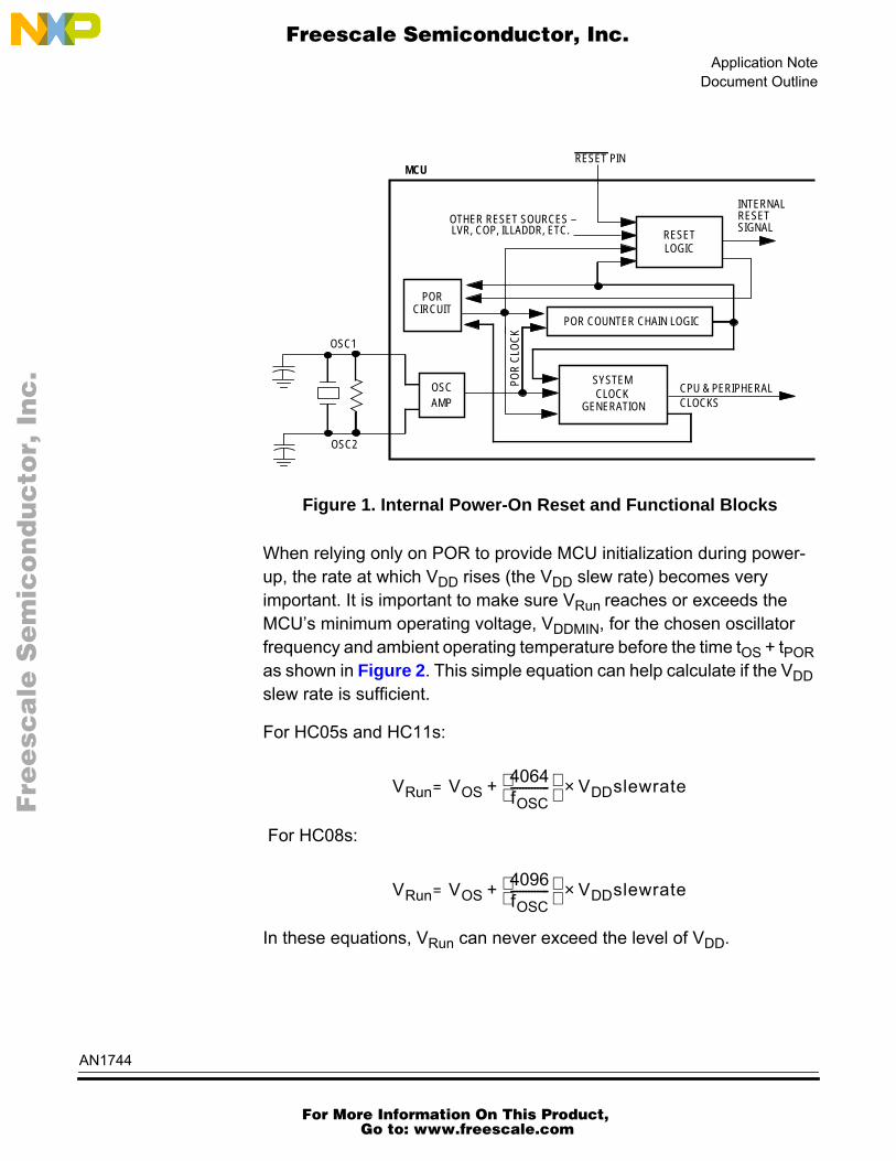
The power-on reset function is accomplished through the use of severalcircuits inside the MCU. The three main components of this function are:
1. POR circuit
2. POR counter chain logic
3. Internal reset logic
Refer to Figure 1 for a block diagram of the components within the MCU.
All HC05s, HC11s, and HC08s contain an internal POR circuit. Thepurpose of the POR circuit is to pre-condition certain logical circuitswithin the MCU as VDD begins to rise. Two of the circuits that are pre-conditioned by the POR circuit are the internal reset generation logic andthe POR counter chain logic.
NOTE: The POR circuit itself does not hold the MCU in reset for any pre-determined amount of time, but the combination of the POR circuit, thePOR counter chain logic, and the MCU’s reset logic will create thepower-on delay (tPOR shown in Figure 2 ).
As seen in Figure 2 , the internal POR signal operates only during theearly stages of power-up. In fact, at just above the voltage level requiredfor the CMOS logic to begin recognizing logical states, this signal will nolonger be asserted. The mechanism that negates the internal PORsignal is feedback from all the circuits that use it, indicating thatinitialization has completed. This all takes place in a short period of timeearly in the power-up sequence.
Once the POR circuit initializes the reset logic, which in turn asserts theinternal reset signal, the POR counter delay logic holds the MCU in areset state for 4064 (HC05 and HC11) or 4096 (HC08) oscillator clock
AN1744
For More Information On This Product,
Go to: www.freescale.com

Application Note
F
ree
sca
le S
em
ico
nd
uc
tor,
I
Freescale Semiconductor, Inc.n
c..
.
cycles during the power-up sequence. This is referred to in mostdatabooks as the oscillator stabilization time. The time, tPOR, will varydepending on the crystal frequency used, the voltage at whichoscillations start, and the VDD rise time.
Because the purpose of the POR circuit is only to precondition internalcircuits/logic, it will not detect a loss of power to the MCU. In fact, the VDDvoltage must fall to a level much below the logic operating level, usuallyabout 0.2 V, and remain there for several tens of milliseconds to re-armitself to detect the next rise of VDD. A temporary loss of VDD, sometimescalled brown-out, can cause internal logic storage elements to changestate and thus potentially disrupt proper MCU operation. In this case,which is covered in this application note’s section on Influences onReset During Power Down on page 13 , an LVR circuit is required toprotect the MCU and give it a clean reset.
System Power-UpSequence
As the MCU begins to experience a rising voltage on its VDD pin, severalthings begin to happen:
• Once VDD reaches a level sufficient for the CMOS logic to beginoperating (~1-V range, typically), the internal oscillator circuits willbegin to oscillate regardless of the type of oscillator used (crystal,ceramic resonator, resistor capacitor (RC), etc.). This voltage isgiven the term VOS.
• Once the oscillator (and hence the internal systems clocks) beginto run, all internal logic that must be initialized during power-upmust be in the correct logical state.
• At this point, the POR counter chain and reset logic will continueto assert the internal reset signal for a period of 4064 (HC05 andHC11) or 4096 (HC08) POR clock cycles.
• Once this period of time (which depends on the oscillatorfrequency) has expired, the POR circuit will negate its input intothe reset logic.
• If no other sources of reset occur, the MCU will come out of resetand the CPU will begin executing code.
AN1744
4 For More Information On This Product,
Go to: www.freescale.com
Application NoteDocument Outline
F
ree
sca
le S
em
ico
nd
uc
tor,
I
Freescale Semiconductor, Inc.n
c..
.
Figure 1. Internal Power-On Reset and Functional Blocks
When relying only on POR to provide MCU initialization during power-up, the rate at which VDD rises (the VDD slew rate) becomes veryimportant. It is important to make sure VRun reaches or exceeds theMCU’s minimum operating voltage, VDDMIN, for the chosen oscillatorfrequency and ambient operating temperature before the time tOS + tPORas shown in Figure 2 . This simple equation can help calculate if the VDDslew rate is sufficient.
For HC05s and HC11s:
For HC08s:
In these equations, VRun can never exceed the level of VDD.
OSCAMP
POR
INTERNALRESETSIGNAL
POR COUNTER CHAIN LOGICCIRCUIT
RESETLOGIC
SYSTEMCLOCK
GENERATION
OTHER RESET SOURCES –LVR, COP, ILLADDR, ETC.
CPU & PERIPHERALCLOCKS
MCURESET PIN
POR
CLO
CK
OSC1
OSC2
VRun VOS4064fOSC-------------
+ VDDslewrate×=
VRun VOS4096fOSC-------------
+ VDDslewrate×=
AN1744
For More Information On This Product,
Go to: www.freescale.com
Application Note
F
ree
sca
le S
em
ico
nd
uc
tor,
I
Freescale Semiconductor, Inc.n
c..
.
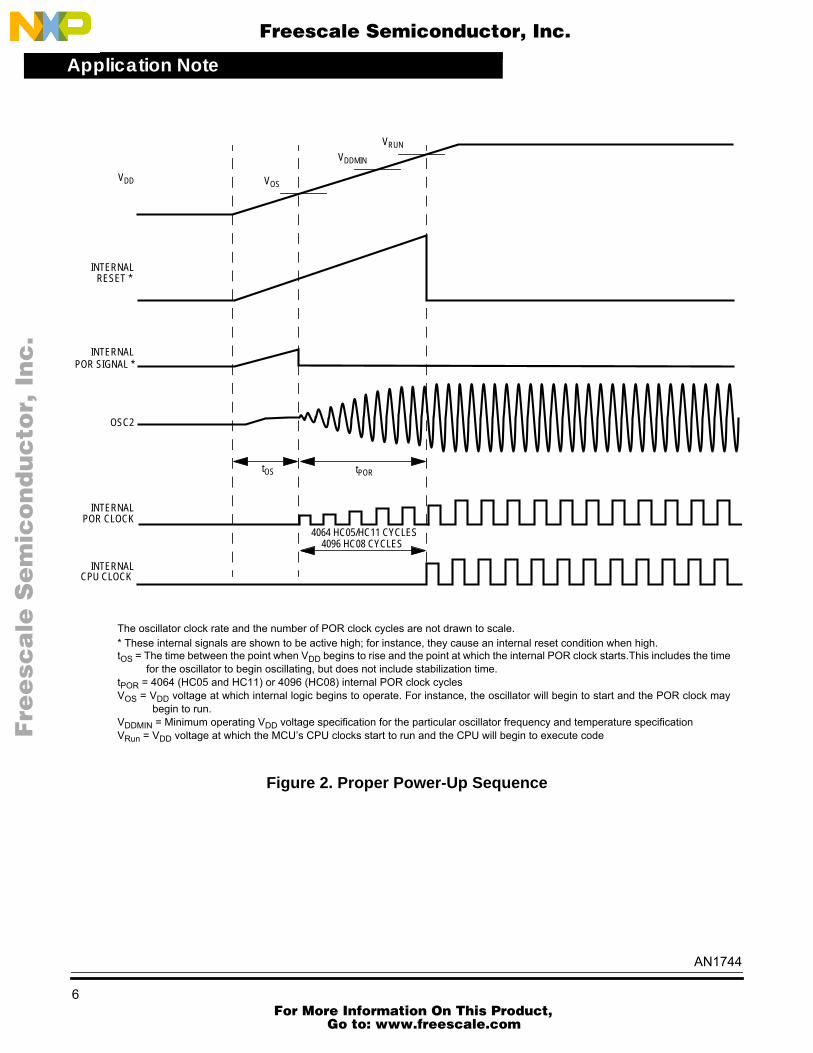
Figure 2. Proper Power-Up Sequence
tOS tPOR
VOS
VRUN
tOS = The time between the point when VDD begins to rise and the point at which the internal POR clock starts.This includes the timefor the oscillator to begin oscillating, but does not include stabilization time.
tPOR = 4064 (HC05 and HC11) or 4096 (HC08) internal POR clock cyclesVOS = VDD voltage at which internal logic begins to operate. For instance, the oscillator will begin to start and the POR clock may
begin to run.VDDMIN = Minimum operating VDD voltage specification for the particular oscillator frequency and temperature specificationVRun = VDD voltage at which the MCU’s CPU clocks start to run and the CPU will begin to execute code
INTERNALPOR SIGNAL *
VDDMIN
4064 HC05/HC11 CYCLES4096 HC08 CYCLES
The oscillator clock rate and the number of POR clock cycles are not drawn to scale.* These internal signals are shown to be active high; for instance, they cause an internal reset condition when high.
VDD
INTERNALRESET *
OSC2
INTERNALPOR CLOCK
INTERNALCPU CLOCK
AN1744
6 For More Information On This Product,
Go to: www.freescale.com
Application NoteDocument Outline
F
ree
sca
le S
em
ico
nd
uc
tor,
I
Freescale Semiconductor, Inc.n
c..
.
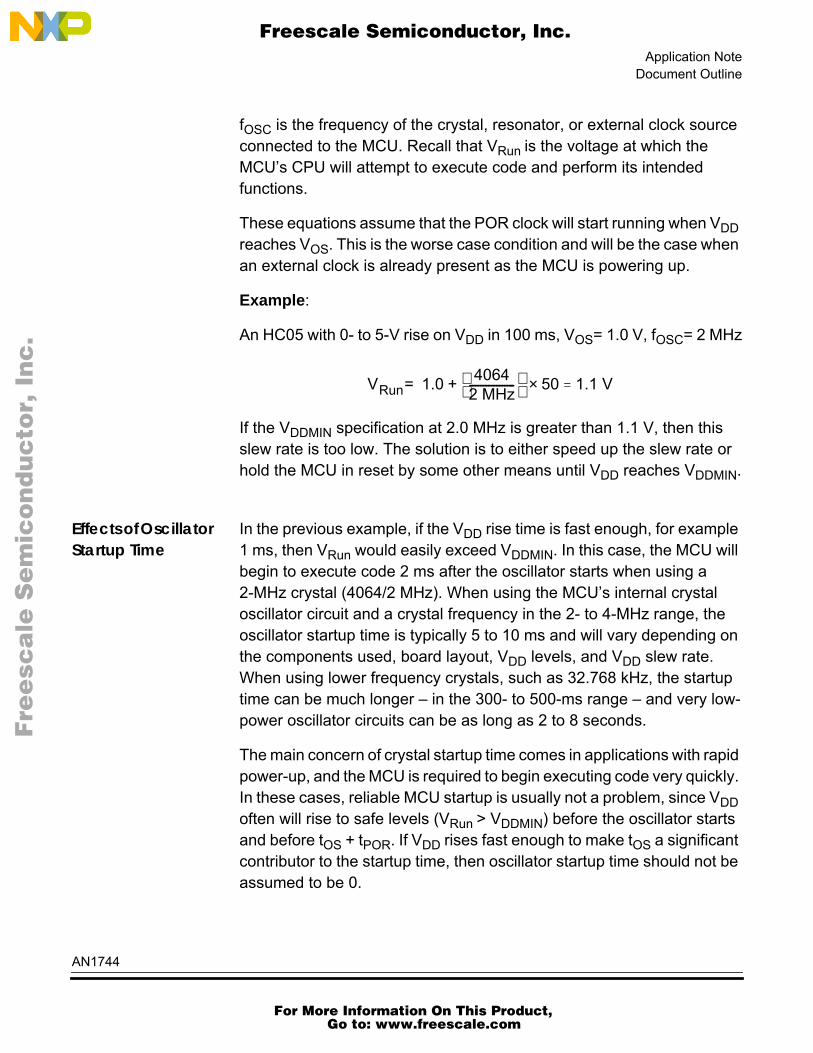
fOSC is the frequency of the crystal, resonator, or external clock sourceconnected to the MCU. Recall that VRun is the voltage at which theMCU’s CPU will attempt to execute code and perform its intendedfunctions.
These equations assume that the POR clock will start running when VDDreaches VOS. This is the worse case condition and will be the case whenan external clock is already present as the MCU is powering up.
Example :
An HC05 with 0- to 5-V rise on VDD in 100 ms, VOS= 1.0 V, fOSC= 2 MHz
If the VDDMIN specification at 2.0 MHz is greater than 1.1 V, then thisslew rate is too low. The solution is to either speed up the slew rate orhold the MCU in reset by some other means until VDD reaches VDDMIN.
Effects of OscillatorStartup Time
In the previous example, if the VDD rise time is fast enough, for example1 ms, then VRun would easily exceed VDDMIN. In this case, the MCU willbegin to execute code 2 ms after the oscillator starts when using a2-MHz crystal (4064/2 MHz). When using the MCU’s internal crystaloscillator circuit and a crystal frequency in the 2- to 4-MHz range, theoscillator startup time is typically 5 to 10 ms and will vary depending onthe components used, board layout, VDD levels, and VDD slew rate.When using lower frequency crystals, such as 32.768 kHz, the startuptime can be much longer – in the 300- to 500-ms range – and very low-power oscillator circuits can be as long as 2 to 8 seconds.
The main concern of crystal startup time comes in applications with rapidpower-up, and the MCU is required to begin executing code very quickly.In these cases, reliable MCU startup is usually not a problem, since VDDoften will rise to safe levels (VRun > VDDMIN) before the oscillator startsand before tOS + tPOR. If VDD rises fast enough to make tOS a significantcontributor to the startup time, then oscillator startup time should not beassumed to be 0.
VRun 1.0 40642 MHz-----------------
+ 50 1.1 V=×=
AN1744
For More Information On This Product,
Go to: www.freescale.com
Application Note
F
ree
sca
le S
em
ico
nd
uc
tor,
I
Freescale Semiconductor, Inc.n
c..
.
In the cases when VDD is rising at a moderate rate and tOS + tPOR isabout the same as the oscillator startup time, it is best to assume thatthe oscillator will start immediately when VDD reaches VOS. Takeprecautions to make sure the MCU is held in the reset state until VDDsafely reaches VDDMIN.
External Reset If the POR counter chain times out and the MCU’s VDD level is not in asafe operating range, it is the job of some other mechanism (eitherinternal or external) to continue to hold the MCU in a reset state until VDDhas reached VDDMIN. As mentioned earlier, the VDDMIN level will dependon the MCU’s voltage, temperature, and frequency specifications.
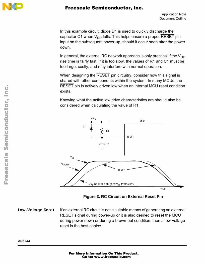
In the case of the external reset pin, a simple and low-cost way to ensurethat the device stays in reset long enough is to put an RC delay on thereset pin as shown in Figure 3 . The component values must be chosento create enough delay to keep the RESET input below the VILspecification (typically 0.2 x VDD) until VDD reaches VDDMIN.
One consideration when choosing the values of R1 and C1 is to ensurethat R1’s value does not get too high and interfere with its ability to drivethe RESET pin high given the worst case input leakage current of thepin. For example, if R1 is 100 Kohms, VDD is 4.8 V, and the input leakagespecification is 1 µA, then the input voltage on the RESET pin will be aminimum of 4.8 – (100 K x 1 µA) = 4.7 V.
This would be acceptable, but R1 values of 500 K or 1 M could possiblycreate an input level on the RESET pin that would be below the VIHspecification.
In addition, the capacitor C1 also should not get too large when usingMCUs that have an active internal RESET pin pull down device. In thiscase, the surge current from the cap into the RESET pin when the pulldown device turns on may be too large and may damage the pincircuitry. In general, limiting this current to less than 25 mA will besufficient.
AN1744
8 For More Information On This Product,
Go to: www.freescale.com
Application NoteDocument Outline
F
ree
sca
le S
em
ico
nd
uc
tor,
I
Freescale Semiconductor, Inc.n
c..
.
In this example circuit, diode D1 is used to quickly discharge thecapacitor C1 when VDD falls. This helps ensure a proper RESET pininput on the subsequent power-up, should it occur soon after the powerdown.
In general, the external RC network approach is only practical if the VDDrise time is fairly fast. If it is too slow, the values of R1 and C1 must betoo large, costly, and may interfere with normal operation.
When designing the RESET pin circuitry, consider how this signal isshared with other components within the system. In many MCUs, theRESET pin is actively driven low when an internal MCU reset conditionexists.
Knowing what the active low drive characteristics are should also beconsidered when calculating the value of R1.
Figure 3. RC Circuit on External Reset Pin
Low-Voltage Reset If an external RC circuit is not a suitable means of generating an externalRESET signal during power-up or it is also desired to reset the MCUduring power down or during a brown-out condition, then a low-voltagereset is the best choice.
MCU
RESET
+VDD
D1R1
C1
VDD
RESET
TIME
< VIL OF RESET PIN (0.2 X VDD TYPICALLY)
>VDDMIN
AN1744
For More Information On This Product,
Go to: www.freescale.com
Application Note
F
ree
sca
le S
em
ico
nd
uc
tor,
I
Freescale Semiconductor, Inc.n
c..
.
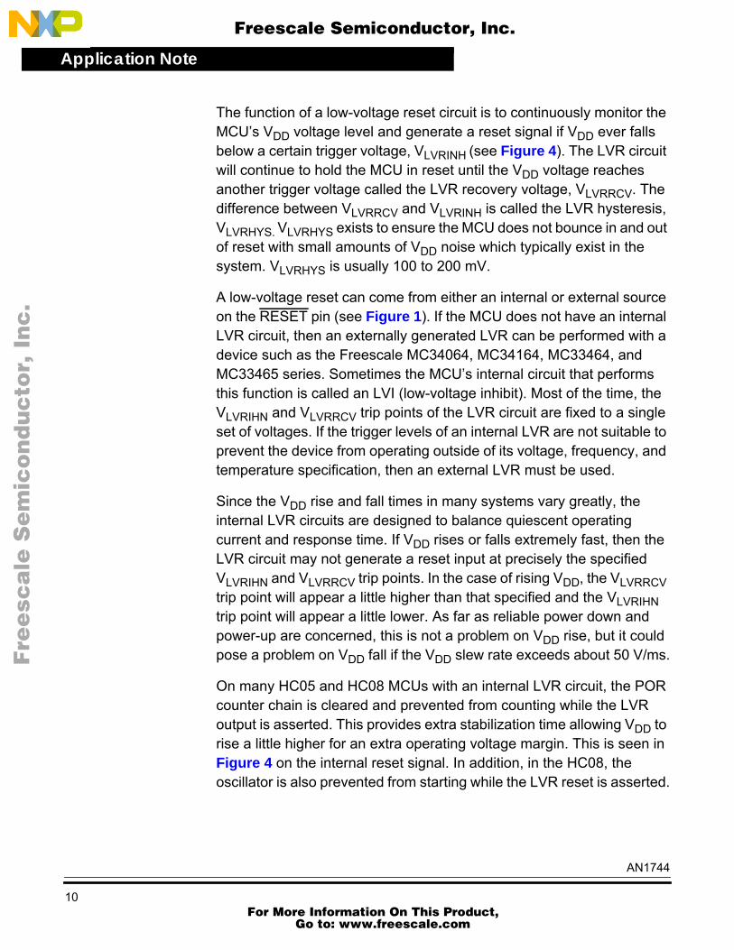
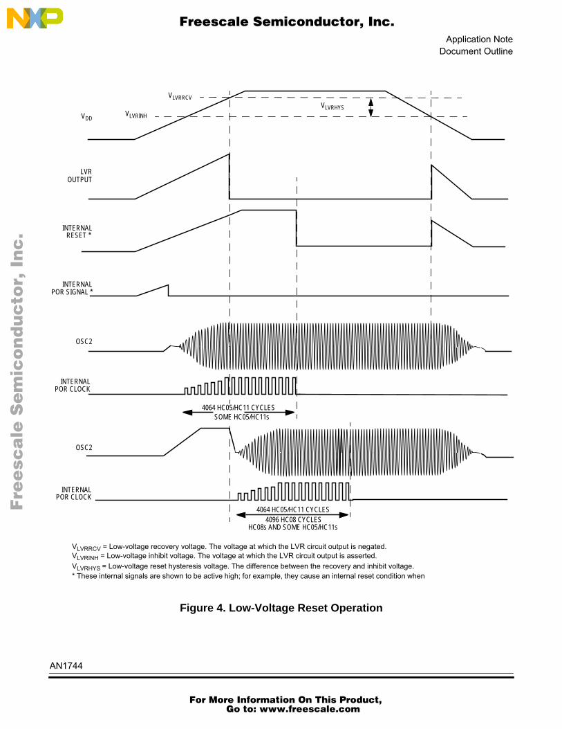
The function of a low-voltage reset circuit is to continuously monitor theMCU’s VDD voltage level and generate a reset signal if VDD ever fallsbelow a certain trigger voltage, VLVRINH (see Figure 4 ). The LVR circuitwill continue to hold the MCU in reset until the VDD voltage reachesanother trigger voltage called the LVR recovery voltage, VLVRRCV. Thedifference between VLVRRCV and VLVRINH is called the LVR hysteresis,VLVRHYS. VLVRHYS exists to ensure the MCU does not bounce in and outof reset with small amounts of VDD noise which typically exist in thesystem. VLVRHYS is usually 100 to 200 mV.
A low-voltage reset can come from either an internal or external sourceon the RESET pin (see Figure 1 ). If the MCU does not have an internalLVR circuit, then an externally generated LVR can be performed with adevice such as the Freescale MC34064, MC34164, MC33464, andMC33465 series. Sometimes the MCU’s internal circuit that performsthis function is called an LVI (low-voltage inhibit). Most of the time, theVLVRIHN and VLVRRCV trip points of the LVR circuit are fixed to a singleset of voltages. If the trigger levels of an internal LVR are not suitable toprevent the device from operating outside of its voltage, frequency, andtemperature specification, then an external LVR must be used.
Since the VDD rise and fall times in many systems vary greatly, theinternal LVR circuits are designed to balance quiescent operatingcurrent and response time. If VDD rises or falls extremely fast, then theLVR circuit may not generate a reset input at precisely the specifiedVLVRIHN and VLVRRCV trip points. In the case of rising VDD, the VLVRRCVtrip point will appear a little higher than that specified and the VLVRIHNtrip point will appear a little lower. As far as reliable power down andpower-up are concerned, this is not a problem on VDD rise, but it couldpose a problem on VDD fall if the VDD slew rate exceeds about 50 V/ms.
On many HC05 and HC08 MCUs with an internal LVR circuit, the PORcounter chain is cleared and prevented from counting while the LVRoutput is asserted. This provides extra stabilization time allowing VDD torise a little higher for an extra operating voltage margin. This is seen inFigure 4 on the internal reset signal. In addition, in the HC08, theoscillator is also prevented from starting while the LVR reset is asserted.
AN1744
10 For More Information On This Product,
Go to: www.freescale.com
Application NoteDocument Outline
F
ree
sca
le S
em
ico
nd
uc
tor,
I
Freescale Semiconductor, Inc.n
c..
.
Figure 4. Low-Voltage Reset Operation
VDD
LVROUTPUT
VLVRINH
VLVRRCV = Low-voltage recovery voltage. The voltage at which the LVR circuit output is negated.VLVRINH = Low-voltage inhibit voltage. The voltage at which the LVR circuit output is asserted.VLVRHYS = Low-voltage reset hysteresis voltage. The difference between the recovery and inhibit voltage.* These internal signals are shown to be active high; for example, they cause an internal reset condition when
INTERNALPOR SIGNAL *
VLVRRCVVLVRHYS
OSC2
INTERNALRESET *
INTERNALPOR CLOCK
4064 HC05/HC11 CYCLES
OSC2
INTERNALPOR CLOCK
4064 HC05/HC11 CYCLES
SOME HC05/HC11s
HC08s AND SOME HC05/HC11s4096 HC08 CYCLES
AN1744
For More Information On This Product,
Go to: www.freescale.com
Application Note
F
ree
sca
le S
em
ico
nd
uc
tor,
I
Freescale Semiconductor, Inc.n
c..
.
Effects of MaskOption Registeron the LVRin OTP Devices
Several Freescale MCUs with internal LVR circuits have a version thatuses some sort of internal non-volatile memory as the main usermemory:
• MC68HC705xx
• MC68HC805xx
• MC68HC908xx
These are commonly referred to as OTP (one-time programmable)devices. Because these devices do not have to go through a mask ROMcycle in the fabrication process to install application software and selectmask options, the mask options in some MCUs are implemented in thesame non-volatile memory bit cells that are used to build the mainmemory array. The non-volatile register that contains the mask optionbits are called the mask option register (MOR). Many times, an LVRenable/disable bit will be present in the MOR.
During power-up and periodically thereafter, these non-volatile, MORbits are read and periodically refreshed. The logical state of the non-volatile bit is copied into a static latch. The output of the static latchcontrols the circuitry to which the MOR bit is connected.
Since some HC05 MCUs with internal LVR circuits were not designedoriginally for excessively slow VDD rise and fall times, this may pose aproblem in these applications because the MOR signals that enable theLVR are not available until VDD reaches the 2.0- to 2.5-V level and theinternal clocks begin to run.
There are two reasons for this:
• First, many times the MOR bits are built into the main memoryarray and the MCU’s internal clocks must be running and VDDvoltage must be at a sufficient level to read the memory array.
• Second, the VDD level required to read a non-volatile memory bitis usually higher than that required to read a mask programmedoption bit. Consequently, the operation of the MOR bits can onlybe guaranteed down to a specific VDD level.
As a result, an MCU with an LVR enable/disable bit in the MOR will workbetter to emulate LVR functions during power down than during power-
AN1744
12 For More Information On This Product,
Go to: www.freescale.com

Application NoteDocument Outline
F
ree
sca
le S
em
ico
nd
uc
tor,
I
Freescale Semiconductor, Inc.n
c..
.
up. However, it also has its limitations during power down. In thosecases, the LVR will operate properly to a point. Then, due to the refreshoperation, the MOR bit may turn off the LVR, which could release theinternal reset signal.
If the VDD rise and fall times are slow, then it is best to use an externalRC circuit on the RESET pin or an external LVR circuit when dealing withsome HC05 OPT devices.
In the mask ROM equivalent device, the LVR can be used safely forpower-up as well as power down.
In the case of the MC68HC908xx Family of MCUs, the LVR MORenable/disable bit, which is implemented with only a static latch and nonon-volatile bit, is contained in the CONFIG register. This bit is initializedto enable the LVR during a POR reset and must be turned off bysoftware if the LVR operation is not required. This approach is robustduring power transitions but is not as immune to sudden and severe VDDtransients or brown-out conditions as the implementation, which usesthe non-volatile bit with periodic refresh.
Influenceson Reset DuringPower Down
In addition to encountering problems during power-up, the applicationdesigner also must consider the possibility of the MCU operatingincorrectly as the system is powering down.
System ProtectionMechanisms
Fortunately, there are robust means of protecting the system duringpower loss that are readily available. Among them are the use of thecomputer operating properly (COP) function, illegal address reset (IAR),or illegal instruction reset (IIR,) and the LVR circuit. The COP, IAR, andIIR are available on nearly all HC05, HC11, and HC08 devices andshould be used to protect the system not only during power transitionsbut under normal operating conditions.
As VDD begins to fall, the MCU may begin to operate outside of itsspecified operating range (VDD falls below VDDMIN). When this happens,the internal circuits may not perform as expected and could result in theMCU performing erratically and erroneously. If the COP, IAR, or IIR arein use, then the MCU will receive a reset before it operates under this
AN1744
For More Information On This Product,
Go to: www.freescale.com
Application Note
F
ree
sca
le S
em
ico
nd
uc
tor,
I
Freescale Semiconductor, Inc.n
c..
.
condition very long. It can take anywhere between one to several cycles,even several hundreds or thousands of cycles, before a reset from COP,IAR, or IIR will be asserted. In the case of a COP reset, it depends onwhen the COP was last serviced. In the case of IAR or IIR, it will dependon how long it takes for erroneous data to be read from memory orinterpreted by the CPU. There is no way to predict how long this will take.
In many applications, especially those in which VDD falls to VOS rapidly,this is not an issue, since not many CPU clock cycles will elapse duringthe power down time.
LVR During PowerDown
In applications which are not tolerant of even a single erroneous cycle,the use of either an internal or external LVR will protect the system evenfurther. As shown in Figure 4 , if the VLVRINH voltage is at or above theminimum operating voltage of the MCU VDDMIN, then the system will beforced into a reset once VDD falls to an unsafe level.
ProtectingNon-VolatileMemory
One of the MCU’s common subsystems – on-chip erasable andprogrammable EEPROM or FLASH memory – can be particularlyvulnerable to permanent data corruption during power loss. This is onlya problem when the on-board memory is in the process of being altered(programmed or erased) during a power down. Since it usually takes 10ms or more to perform a program or erase operation, there is a widewindow of opportunity to lose power and interrupt the program or erasesequence. Even if the system makes use of an LVR to prevent erraticMCU operation during power down, there is no guarantee that a programor erase operation can complete successfully before the LVR resetoccurs.
One way of preventing this problem is to use an LVR circuit not as ahardware source of reset but to serve as an indicator to the software. Onmany devices, the LVR status bit can be polled to predict when VDD hasstarted to fall, and the software can decide whether a program or eraseoperation has time to occur before VDD is below VDDMIN. Once thedecision and action have been taken, the software can put the MCU intoreset by using external circuitry.
AN1744
14 For More Information On This Product,
Go to: www.freescale.com

Application NoteDocument Outline
F
ree
sca
le S
em
ico
nd
uc
tor,
I
Freescale Semiconductor, Inc.n
c..
.
AN1744
For More Information On This Product,
Go to: www.freescale.com

N
ON
-D
IS
CL
OS
UR
E
AG
RE
EM
EN
T
RE
QU
IR
ED
Application Note
F
ree
sca
le S
em
ico
nd
uc
tor,
I
Freescale Semiconductor, Inc.n
c..
.
For More Information On This Product,
Go to: www.freescale.com