Embed Size (px)
Citation preview
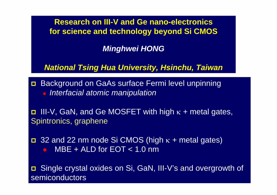
Research on III-V and Ge nano-electronics for science and technology beyond Si CMOS
Minghwei HONG
National Tsing Hua University, Hsinchu, Taiwan
Background on GaAs surface Fermi level unpinningInterfacial atomic manipulation
III-V, GaN, and Ge MOSFET with high κ + metal gates, Spintronics, graphene
32 and 22 nm node Si CMOS (high κ + metal gates)MBE + ALD for EOT < 1.0 nm
Single crystal oxides on Si, GaN, III-V’s and overgrowth of semiconductors

Intel (Sematech) Transistor Scaling and Research Roadmap
More non-silicon elements introduced
(production) (production)(development)
SiO2running out of atoms
EOT=1.0nmInterfacial 0.5nm, Bulk high k ~2.5nm

1960 Kahng and Atalla, Bell Labs First MOSFET
Device Scaling – Beyond 22 nm node: high k, metal gates, and high mobility channel
Moore’s Law: The number of transistors per square inch doubles every 18 months
Shorter gate length L Thinner gate dielectrics tox
Driving force :High speedLower power consumptionHigh package density
Oxide/semiconductor Interface ⇒ perfection
Metal gate
High mobilitychannel
Higher κ gatedielectric
Integration of IIIV, Ge with Si

Electron mobilities in GaAs, Si, and Ge
Solid curve: theory with combined polar and ionized-impurity scattering (Ehrenreich: JAP 32, 2155, 1961) Experimental points o: Reid and Willardson: J. Electronics and Control, 5, 54 (1958)▲: Weisberg, Rosi, and Herkart: Metallurgical Soc. Conf., v.5 “Properties of elemental and compound semiconductors, Interscience Publishers, New York, p.275
GaAs Si and GeMeasured drift
mobility in Si and Ge(F. J. Morin and J. P.
Maita, Phys. Rev.,94, 1526, (1954) and
96, 28 (1954))
T -2.3─T -2.7T -2.5T -2.33T -1.66Temperature dependence
3408500470140019003900value at 300K
μpμnμpμnμpμn
GaAsSiGeDRIFT MOBILITIES (cm2/ V-s) in Ge, Si, and GaAs at 300K

Do we need a new methodology for GaAs passivation?A. M. Green and W. E. SpicerStanford UniversityJVST A11(4), 1061, 1993
“A new methodology for passivating compound semiconductors is presented in which two overlayers are used. In this approach, the first layer defines the surface electronically and the second provides long term protection.”
Sulfur passivation –Sandroff et al, Bell Labs APL51, 33, 1987Sb passivation – Cao et al, Stanford Surf. Sci. 206, 413, 1988
Is it possible to have a III-V (GaAs) MOS, similar to SiO2/Si, in which a low Dit, a low electrical leakage current density, thermodynamic stability at high temp. (>800°C), single layer of gate dielectric, no S and Sb, etc are achievable?
YES!!!Is it necessary to have GeON as an interfacial layer in Ge MOS? No!!!

Pioneering work of GaAs and InGaAs MOSFET’s using Ga2O3(Gd2O3) at Bell Labs with single overlayer
• 1994 – novel oxide Ga2O3(Gd2O3) to effectively passivate GaAs surfaces
• 1995 – establishment of accumulation and inversion in p- and n-channels in Ga2O3(Gd2O3)-GaAs
MOS diodes with a low Dit of 2-3 x 1010 cm-2 eV-1(IEDM)• 1996
– first e-mode GaAs MOSFETs in p- and n-channels with inversion (IEDM)– Thermodynamically stable
• 1997– e-mode inversion-channel n-InGaAs/InP MOSFET with gm= 190 mS/mm, Id = 350 mA/mm,
and mobility of 470 cm2/Vs (DRC, EDL)• 1998
– d-mode GaAs MOSFETs with negligible drain current drift and hysteresis (IEDM)– e-mode GaAs MOSFETs with improved drain current (over 100 times)– Dense, uniform microstructures; smooth, atomically sharp interface; low leakage currents
• 1999– GaAs power MOSFET– Single-crystal, single-domain Gd2O3 epitaxially grown on GaAs
• 2000– demonstration of GaAs CMOS inverter
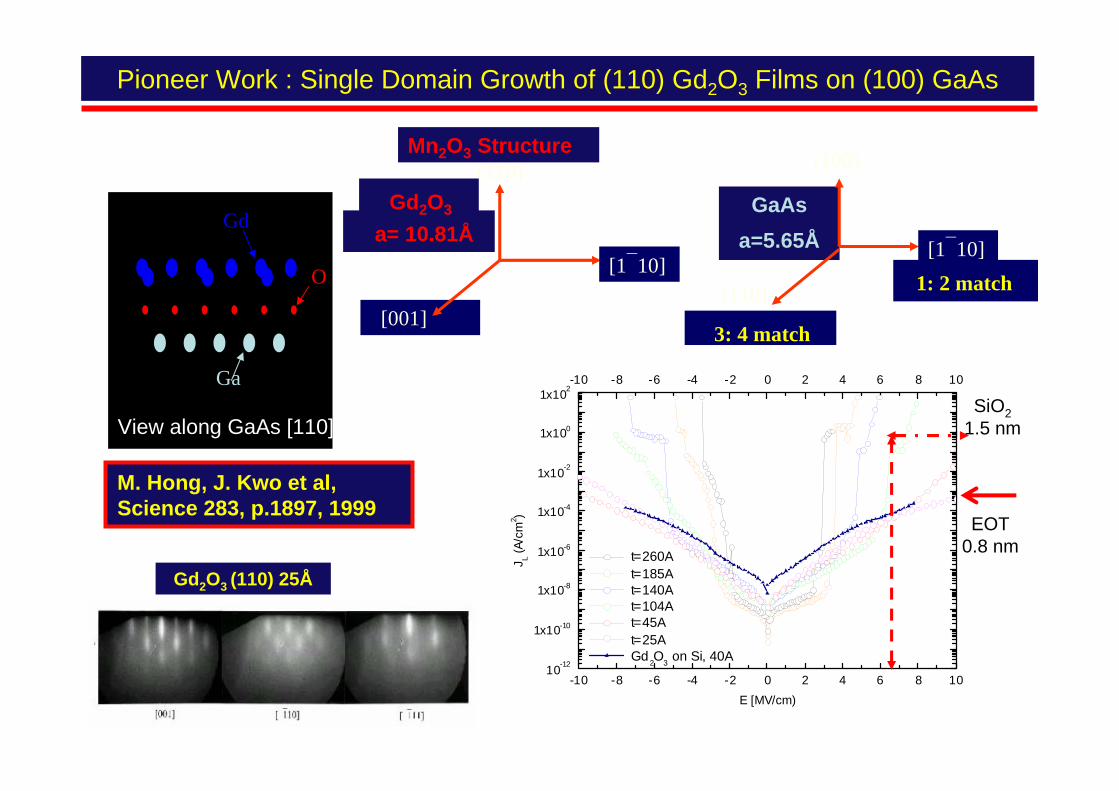
Pioneer Work : Single Domain Growth of (110) Gd2O3 Films on (100) GaAs
GaAsa=5.65Å
[001]
(110)
[1⎯10]a= 10.81Å
1: 2 match
(100)
[110]
[1⎯10]
3: 4 match
O
Gd
Ga
View along GaAs [110]
Gd2O3
Mn2O3 Structure
Gd2O3 (110) 25Å
M. Hong, J. Kwo et al, Science 283, p.1897, 1999
-10 -8 -6 -4 -2 0 2 4 6 8 1010-12
1x10⁻¹⁰
1x10⁻⁸
1x10⁻⁶
1x10⁻⁴
1x10⁻²
1x100
1x10²-10 -8 -6 -4 -2 0 2 4 6 8 10
t=260A t=185A t=140A t=104A t=45A t=25A Gd2O3 on Si, 40A
J L (A/c
m2 )
E [MV/cm)
EOT0.8 nm
SiO21.5 nm

0.2
3 × 10⁷
1300
0.20
3.19
3.40
GaN
μm
cm s-1
cm2
V-1 s-
1
-
Å
eV
units
0.58
5 × 10⁷
78000
0.014
6.50
0.17
InSb
0.27
3 × 10⁷
25000
0.023
6.06
0.354
InAs
0.19
8 × 10⁶
14000
0.041
5.87
0.75
In0.53Ga0.47As
0.15
2 × 10⁷
8500
0.063
5.65
1.43
GaAs
0.07
1 × 10⁷
1500
0.19
5.431
1.12
Si
Electron mean free
path
Electron saturation velocity
Electron mobility
Electron effective
mass
Lattice constant
Energy gap

MBE – compound semiconductor growth – A. Y. Cho (National Medal of Science 1993 and National Medal of Technology 2007)
MBE – metal and oxide growth – J. Kwo (first in discovering anti-ferromagnetic coupling through non-magnetic layer in magnetic superlattices PRL’s 1985 – 1986)
Frank Shu, UC University Professor and former President of Tsing Hua Univ.

oxideoxideMBEMBE
inin--situsituXPSXPS
oxide oxide & metal& metal
MBEMBE
IIIIII--VVMBEMBE
SiSi--GeGeMBEMBE
annealingannealing& metal& metalchamberchamberWafer inWafer in
MultiMulti--chamber MBE/inchamber MBE/in--situ analysis systemsitu analysis system
InIn--situsituSPMSPM SMOKESMOKEmetalmetal
chamberchamber

MultichamberMultichamber Ultrahigh Vacuum SystemUltrahigh Vacuum System1.1. A solid source A solid source GaAsGaAs--based MBE chamberbased MBE chamber2.2. Oxide deposition chamber (AsOxide deposition chamber (As--free)free)3.3. Metal chamberMetal chamber4.4. GeGe--Si ChamberSi Chamber5.5. InIn--situ XPSsitu XPS6.6. InIn--situ SPMsitu SPM7.7. Other functional chambers, Other functional chambers, incl.SMOKEincl.SMOKE8.8. UHV transfer modulesUHV transfer modules

1897 J. J. Thomson discovery of electron
1947 The Transistor
2007 High k + metal gate on 45 nm node CMOS
What next – IIIV, GaN, or Ge MOS in 2017?
Mervin Kelly, the then Director of Res. at Bell Labs, had predicted the problem and had already taken action to find a solution.
Although relays and vacuum tubes were apparently making all things possible in telephony, he hadpredicted for some years that the low speed of relays and the short life and high power consumption of tubes would eventually limit further progress in telephony and other electronic endeavors.
In the summer of 1945, Kelly had established a research group at Bell Labs to focus on the understanding of semiconductors. The group also had a long-term goal of creating a solid-state device that might eventually replace the tube and the relay.

• Surface Fermi level unpinning in III-V’s (the Holy Grail), Ge– UHV deposited Ga2O3(Gd2O3); ALD-HfO2 and Al2O3 on InGaAs;
Ga2O3(Gd2O3)/Ge• Thermodynamic stability of Ga2O3(Gd2O3)/III-V’s; Ge: temp. limit
• Ga2O3(Gd2O3)/InGaAs oxide scalability: EOT scalability • YDH (yttrium doped HfO2) – novel high k gate dielectric• ALD/MBE approach: complete elimination of interfacial layers• Inversion-channel GaAs-based and GaN MOSFET’s• Single crystal oxides on Si(111)
– GaN/gamma- Al2O3, Sc2O3/Si(111); ZnO/- - -/Si (111)• Oxides/GaN• IETS• In-situ SPM, SMOKE, XPS• Spintronics
– Spin LED; Andreev Reflection – Fe3Si/GaAs, magnetic/single crystal oxides/magnetic– Dilute magnetic Co-HfO2– Spin FET

• InGaAs, GaN, and Ge– Surface Fermi level unpinning
• Necessity of interfacial layers– UHV deposited Ga2O3(Gd2O3); ALD-HfO2 and Al2O3
• Electrical characteristics: J-E; C-V; Dit• EOT (CET) scalability
– Thermodynamic stability: temp. limit
• Higher k dielectrics– YDH (yttrium doped HfO2) – novel high k gate dielectric
• ALD/MBE approach: complete elimination of interfacial layers in Si and Ge
• Inversion-channel InGaAs, Ge, and GaN MOSFET’s• Metal gates• Integration of InGaAs, Ge, and GaN with Si• Single crystal oxides on Si(111)
– GaN/gamma- Al2O3, Sc2O3/Si(111); ZnO/- - -/Si (111)• Oxides/GaN• IETS• In-situ SPM, XPS


![Spintronics [EDocFind.com]](https://img.dokumen.tips/doc/110x75/577d2e0b1a28ab4e1eaea99b/spintronics-edocfindcom.jpg)