Embed Size (px)
Citation preview

“Research is to see what everyone else has seen
and think what no one else has thought.”Albert Einstein
Integrated Circuit Outlier Identification by
Multiple Parameter Correlation
Sagar SabadeDepartment of Computer ScienceTexas A&M University, MS 3112 College Station, TX 77843-3112
E-mail: [email protected]
Outline
! Introduction! Problem Definition! Prior Work! Research Goals! Research Plan! Summary

Test: Needle Search In Haystack
~130 nm
Intel® Pentium 4 chip layout
© Intel Corporation
14 mm
14 mm
130 nm technologyMiles of copper interconnect42 million transistors
Particle
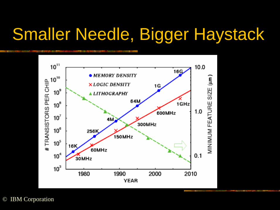
Smaller Needle, Bigger Haystack
© IBM Corporation

Semiconductor Economics 101
! Cost – the prime drive for technology! Manufacturing cost/transistor falls rapidly
! higher performance/cost ratio! Complexity increasing with each technology
advancement! Test cost falls slowly! Increasing test cost contribution to overall cost
! Tester time extremely valuable! Important to find defective chip early in test cycle or
manufacturing flow

Basic Testing Methodology
10101000
(Faulty)Output
Defect detectedonly if outputdifferent from
fault-free output
Input10110101
11101010
and propagate its effect to the output
defect
Apply inputs toexcite the defect
1
0
(Fault-free)Output

So Many Defects, So Little Time
! Billions of possible defects! Fortunately have similar effect on electrical
characteristics! Modeled using higher level of abstraction called
“fault”! Defect " physical (e.g. short between lines)! Fault " electrical (e.g. increased current)
! Many (possible) defects map to the same fault
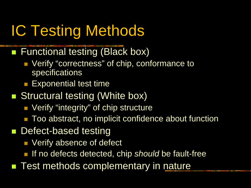
IC Testing Methods! Functional testing (Black box)
! Verify “correctness” of chip, conformance to specifications
! Exponential test time! Structural testing (White box)
! Verify “integrity” of chip structure! Too abstract, no implicit confidence about function
! Defect-based testing! Verify absence of defect! If no defects detected, chip should be fault-free
! Test methods complementary in nature

Defect-based Test Types
! Boolean test! Can distinguish between faulty or fault-free
chips! Continuous parameter test
! No clear faulty/fault-free distinction! Leakage current (IDDQ) test
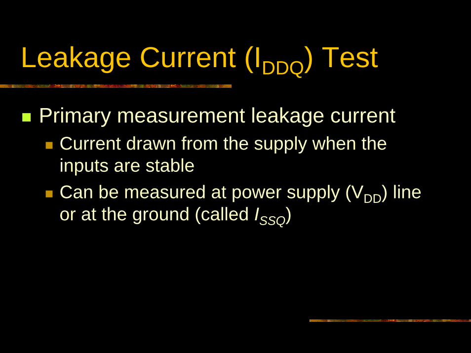
Leakage Current (IDDQ) Test
! Primary measurement leakage current! Current drawn from the supply when the
inputs are stable! Can be measured at power supply (VDD) line
or at the ground (called ISSQ)
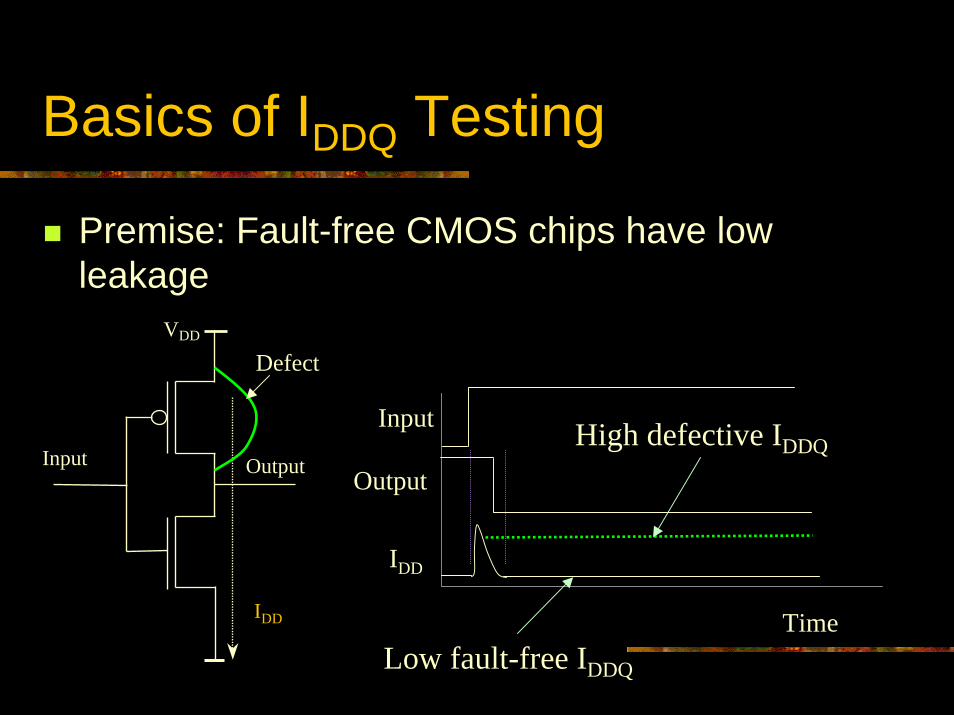
Basics of IDDQ Testing
! Premise: Fault-free CMOS chips have low leakage
IDD
VDD
Input Output
Defect
Input
Output
IDD
TimeLow fault-free IDDQ
High defective IDDQ

Defect Types
! Active (pattern-dependent) defect! Leakage current high for some but not all
patterns! e.g. gate-to-source short, gate oxide short
! Passive (pattern-independent) defect! High leakage current for all input patterns! e.g. VDD-GND short

Advantages of IDDQ Testing
! Simple, intuitive! No propagation requirements
! 100% observability ! Fortuitous detection
! Fewer vectors needed for higher fault detection capability
! Detects several defect types! GOS, stuck-on, punch-through, bridges
! Detects some latent defects! Useful for screening low-reliability chips

Conventional IDDQ Testing
! Single threshold method! Threshold decided using circuit simulations or
empiricallyRejected chips
IDDQ
Chip
Accepted chips
Threshold

Technology Impact on IDDQ Test
! Reduced transistor geometries! Increases leakage current exponentially! Increased process variations
! Cannot distinguish between faulty and fault-free leakage currents using a single threshold
! Small threshold rejects too many good chips! Yield loss (lost revenue)
! High threshold accepts too many flawed chips! Test escapes (customer returns)

ITRS Projections for IDDQ
Year Gate Length (nm) IDDQ
2001 90 30 – 70 mA2003 65 70 – 150 mA2005 45 150 – 400 mA2008 35 400 mA – 1.6A2011 25 1.6 – 8 A2014 15 8 – 20 A
For high-performance microprocessor circuitsSource: Intl. Technology Roadmap for Semiconductors (ITRS) 2001
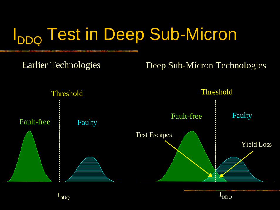
IDDQ Test in Deep Sub-Micron
Fault-free Faulty
Threshold
IDDQ
Earlier Technologies
Fault-free Faulty
Threshold
Test EscapesYield Loss
IDDQ
Deep Sub-Micron Technologies

IDDQ and Defect Severity
0.1 1 1 0 10 0 100 0
1
1 0
10 0
Freq
uenc
y
ID D Q (u A )
Fault-free
Gross defect
Fatally flawedSubtle defect
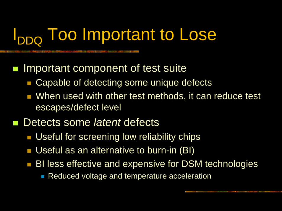
IDDQ Too Important to Lose
! Important component of test suite! Capable of detecting some unique defects! When used with other test methods, it can reduce test
escapes/defect level! Detects some latent defects
! Useful for screening low reliability chips! Useful as an alternative to burn-in (BI)! BI less effective and expensive for DSM technologies
! Reduced voltage and temperature acceleration

IDDQ Only a Part of the Puzzle
InaccurateFault models&NewDefectMechanisms
IncreasedLeakage Test time/data
Reduction &Insufficient Fault coverage
Increased Test cost
Reliability Screens losing effectiveness
ProcessVariability
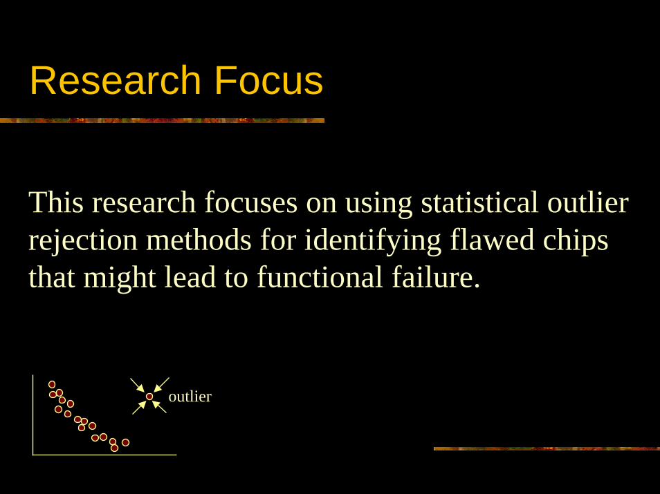
Research Focus
This research focuses on using statistical outlier rejection methods for identifying flawed chipsthat might lead to functional failure.
outlier
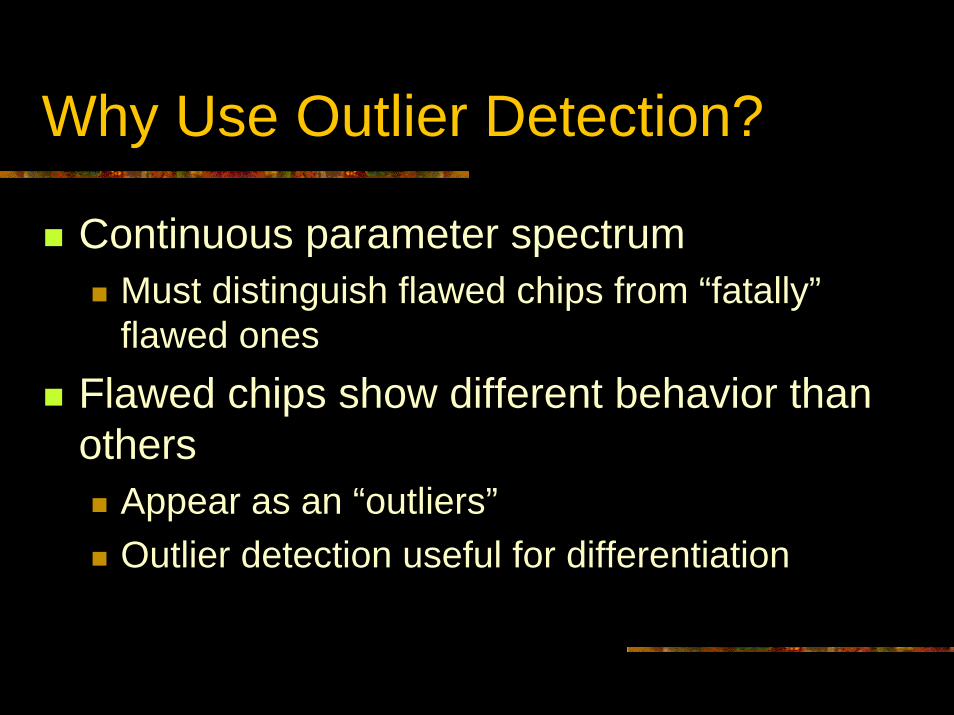
Why Use Outlier Detection?
! Continuous parameter spectrum! Must distinguish flawed chips from “fatally”
flawed ones! Flawed chips show different behavior than
others! Appear as an “outliers”! Outlier detection useful for differentiation
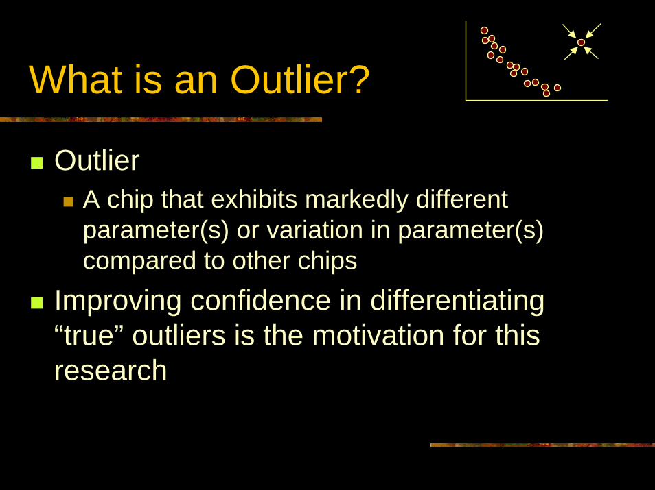
What is an Outlier?
! Outlier! A chip that exhibits markedly different
parameter(s) or variation in parameter(s) compared to other chips
! Improving confidence in differentiating “true” outliers is the motivation for this research

Outlier Identification Methods
! Reliance on properties of standard distributions! Mean, standard deviation, median, range
! Various methods! Z-scores test! Chauvenet’s criterion! Tukey method! Median of Absolute Deviations (MAD) test

Why is Outlier Detection Difficult?
! Outliers affect properties of the distribution! Several orders of magnitude variation in
fault-free IDDQ itself ! Makes difficult to distinguish between a “true”
outlier and an “apparent” outlier! Outliers chips are functionally okay
! Manufacturer’s dilemma (yield loss vs. quality)

No Silver Bullet
0 20 40 600
20
40
60
80
100
120
140
160
180
Freq
uenc
y
IDDQ (µA)
N = 176Mean 2.5 µASTD 8.3
0 2 4 6 80
2
4
6
8
10
Freq
uenc
y
IDDQ (µA)
N = 166Mean 0.84 µASTD 1.43
0.0 0.2 0.4 0.6 0.8 1.0 1.2 1.40
10
20
Freq
uenc
y
IDDQ (µA)
N = 151Mean 0.44 µASTD 0.180 500 1000 1500 2000 2500
0
20
40
60
80
100
120
140
160
180
Freq
uenc
y
IDDQ (µA)
N = 179Mean 19.58 µASTD 176.35
outliers
0 2000 4000 6000 80000
20
40
60
80
100
120
140
160
180
Freq
uenc
y
IDDQ (µA)
N = 197Mean 678 µASTD 2142.65
Wafer level data for a vector
Suggested Solution Methods
! Approach 1! Reduce fault-free IDDQ
! Makes identifying faulty IDDQ easier
! Approach 2! Estimate fault-free IDDQ accurately
! Approach 3! Reduce variation in fault-free IDDQ data
! Makes faulty IDDQ “stand out”! Category known as IDDX

Approach 1: Reducing Fault-free IDDQ
! Reduce temperature! Too expensive, slow, impractical! Less effective for future technologies
! Reverse (back) body bias! Technology change, inflexible! Less effective due to limited backbias voltage
! Silicon-On-Insulator (SOI)! Different technology, learning curve
! Multiple-threshold transistors! Performance tradeoff, less effective in future
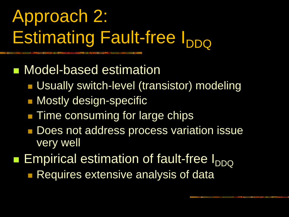
Approach 2: Estimating Fault-free IDDQ
! Model-based estimation! Usually switch-level (transistor) modeling! Mostly design-specific! Time consuming for large chips! Does not address process variation issue
very well! Empirical estimation of fault-free IDDQ
! Requires extensive analysis of data

Die 1 IDDQ Variation
Level 1
Level 2
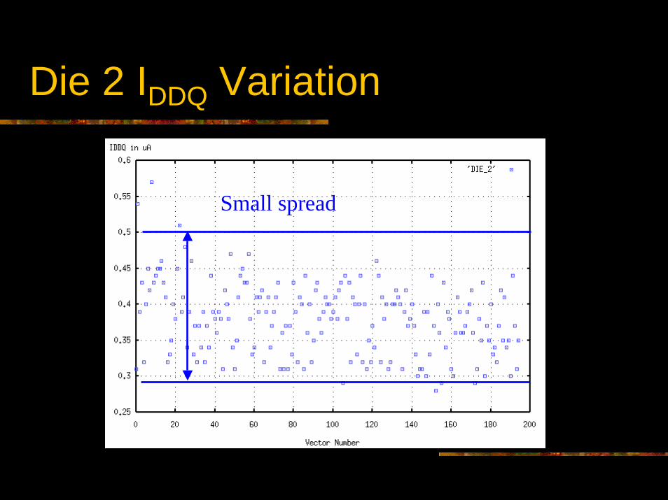
Die 2 IDDQ Variation
Small spread

Die 1 and Die 2 IDDQ Variation
Die 1
Die 2Die 1 readings

Die 1, 2 and 3 IDDQ Variation
Die 3 levels
Is Die 1 really Defective?
Die 1
Die 2
Die 3
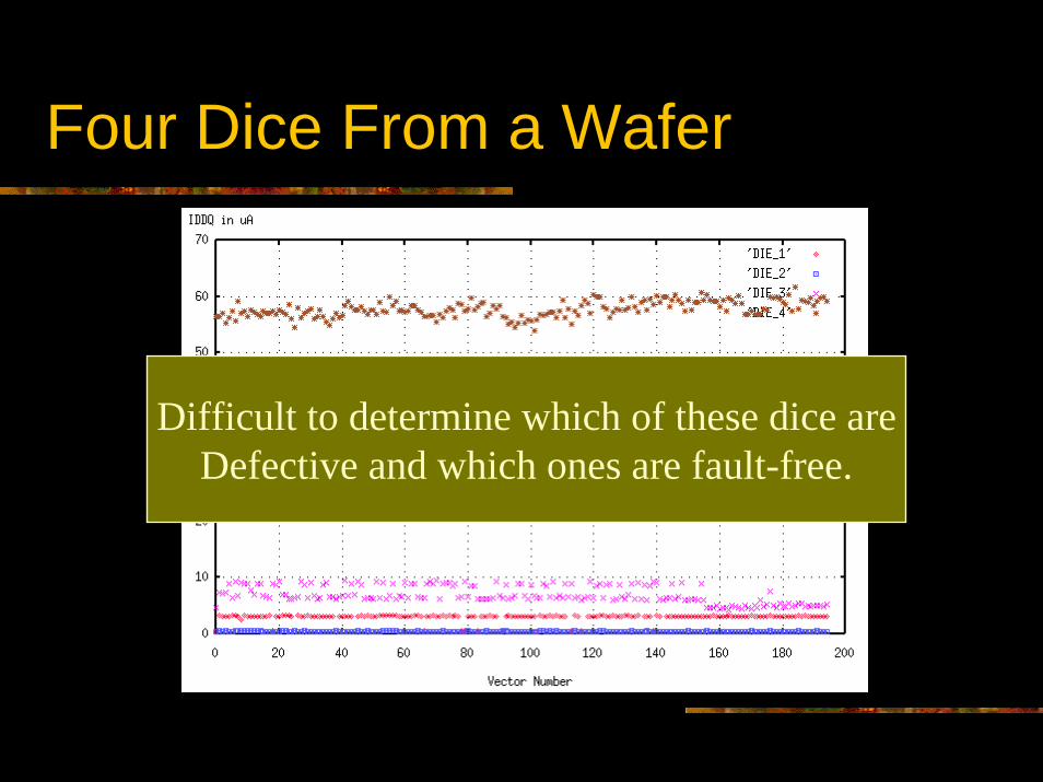
Four Dice From a Wafer
Difficult to determine which of these dice areDefective and which ones are fault-free.
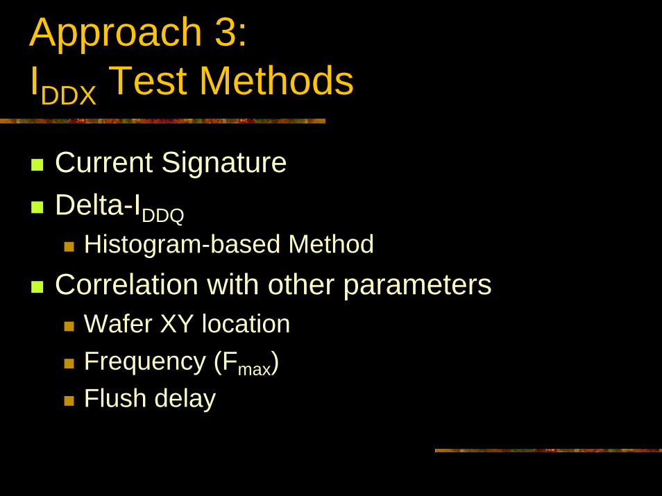
Approach 3: IDDX Test Methods
! Current Signature! Delta-IDDQ
! Histogram-based Method! Correlation with other parameters
! Wafer XY location! Frequency (Fmax)! Flush delay

Current Signature [Gattiker,Maly]
! Signature – sorted IDDQ measurements ! A chip with active defect shows a “step” or
“jump” in the signature! Indicates multiple paths current can take
! Fault-free chip shows smooth signature! Also true for passive defects! Cannot screen passive and subtle active
defects
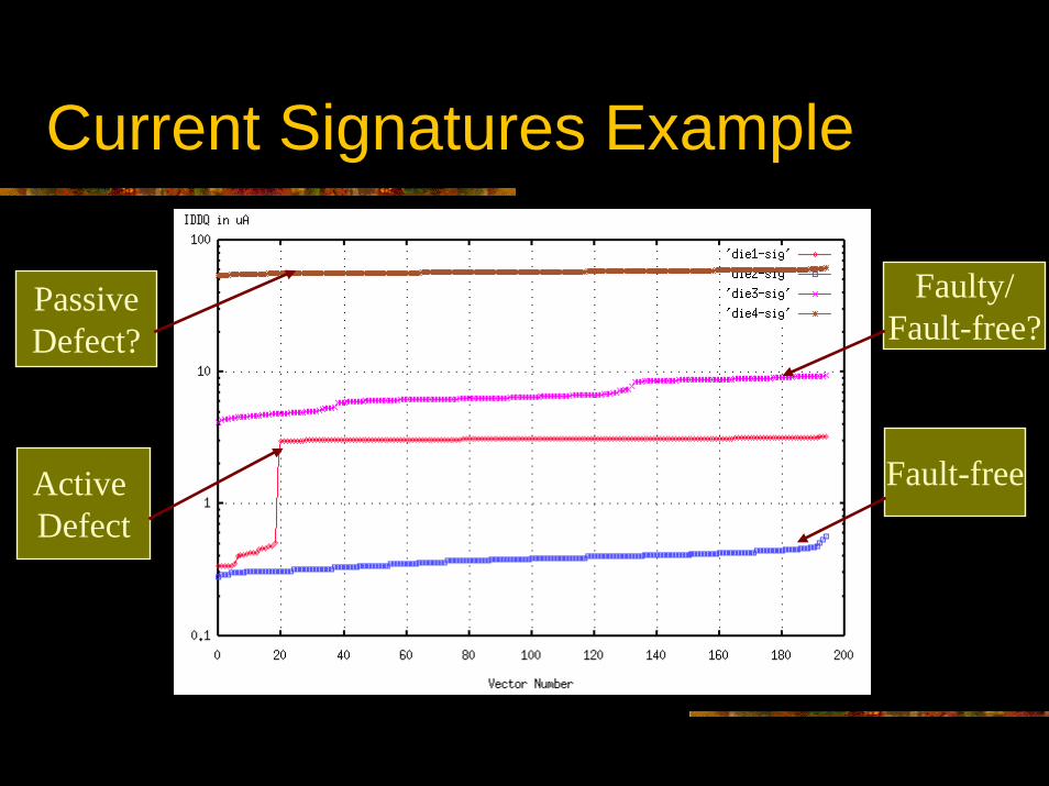
Current Signatures Example
Fault-freeActive Defect
PassiveDefect?
Faulty/Fault-free?
Differential/Delta IDDQ [Thibeault]
! Differences (deltas) in consecutive readings small for a fault-free chip
! Background leakage gets cancelled ! Cannot screen passive defects
! Less effectiveness in future [Krusemann]

Histogram-based Analysis
Frequency
Delta-IDDQ
Reduce σ,Mean ~ 0
0
IDDQ values
IDDQ

Current Ratios [Maxwell et al.]
! CR relatively constant for fault-free chips
! Measure IDDQ for the “minimum IDDQvector” ! Set limits on all other vectors dynamically! Min. IDDQ vector changes from chip to chip
CR = Max IDDQ
Min IDDQ

Current Ratios Example
Courtesy: Peter Maxwell, Agilent Technologies
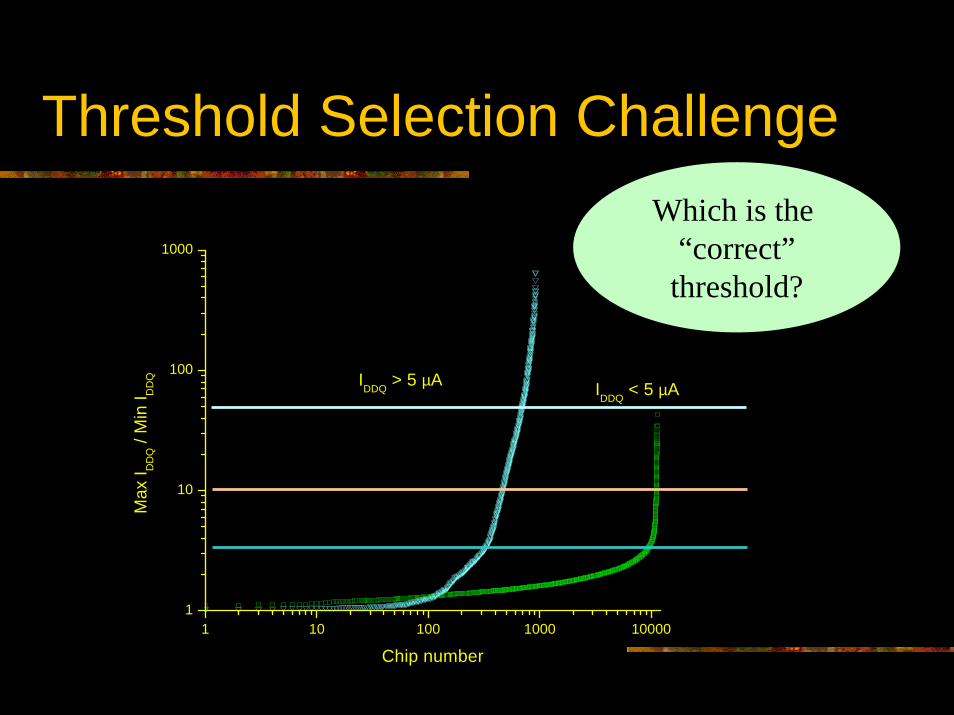
Threshold Selection Challenge
1 10 100 1000 100001
10
100
1000
IDDQ > 5 µA IDDQ < 5 µA
Max
I DD
Q /
Min
I DD
Q
Chip number
Which is the “correct”
threshold?

Outlier Identification by Correlation
! Correlation useful for estimating fault-free IDDQ! Can be used for outlier identification
! Different methods! Vector-to-vector correlation [Unni et al.]! Die-to-die correlation! Die XY position on wafer [Daasch et al.]! Other parameters
! Fmax [Keshavarzi et al.]! Flush delay [Sabade et al.]
Motivation: Spatial Correlation
! Similar process conditions for neighboring chips on a wafer
! Fault-free chip parameters are expected to be similar
! A sudden change in any parameter is indicative of anomalous behavior ! Likely defective [Singh et al.]! Called “spatial outliers”

Spatial Outlier Example
Spatial outliers
2 4 6 810
1214
16
0
10
20
30
40
50
24
68
1012
1416
1820
IDD
Q (µ
A)
Y Coo
dinate
X Coordinate
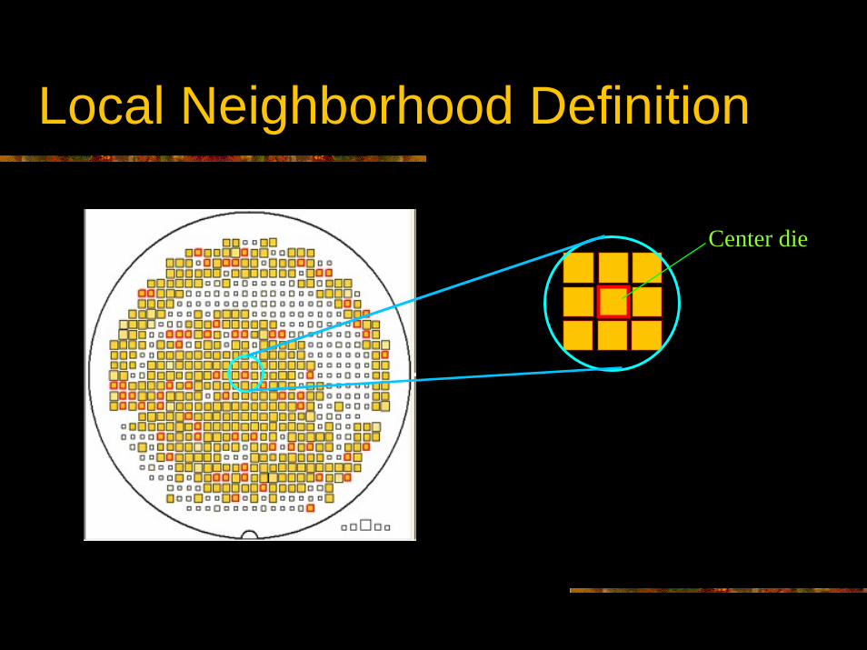
Local Neighborhood Definition
Center die

Estimation of Fault-free IDDQ
! Use neighboring chips’ IDDQ for estimating fault-free IDDQ of the center die! If actual IDDQ is higher, center die is likely to
be defective! If actual IDDQ is lower, neighbor die could be
defective! How high is high? How low is low?
! Threshold setting does not disappear
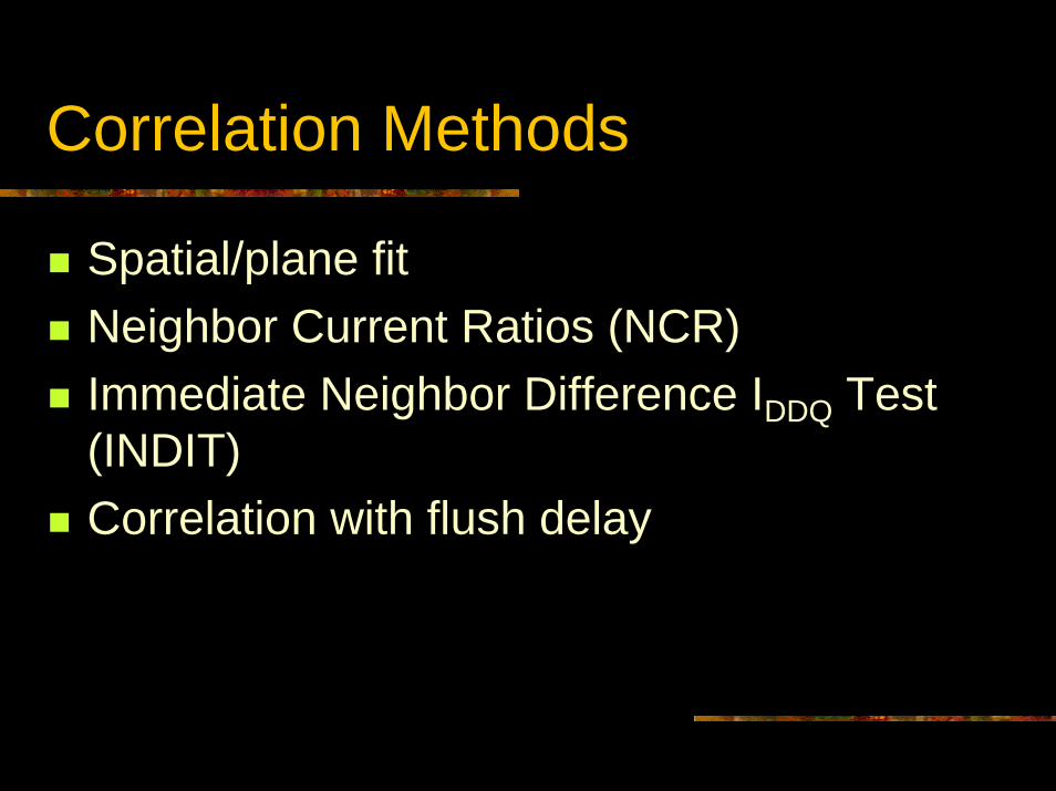
Correlation Methods
! Spatial/plane fit! Neighbor Current Ratios (NCR)! Immediate Neighbor Difference IDDQ Test
(INDIT)! Correlation with flush delay

Plane Fit
! IDDQ function of neighboring dice IDDQ and die’s XY position on wafer! First reject gross outliers! Linear regression
! Z (IDDQ) = A.x + B.y + CX
YIDDQ
wafer
Best fit plane
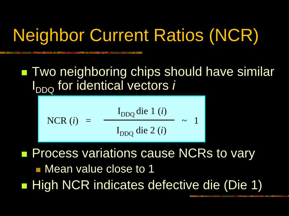
Neighbor Current Ratios (NCR)
! Two neighboring chips should have similar IDDQ for identical vectors i
! Process variations cause NCRs to vary! Mean value close to 1
! High NCR indicates defective die (Die 1)
IDDQ die 1 (i)
IDDQ die 2 (i)~ 1NCR (i) =

NCR Illustration
2 4 6 810
1214
16
0
200
400
600
800
1000
1200
24
68
1012
1416
1820
X
Max
NC
R
Y
Obvious spatial outliers
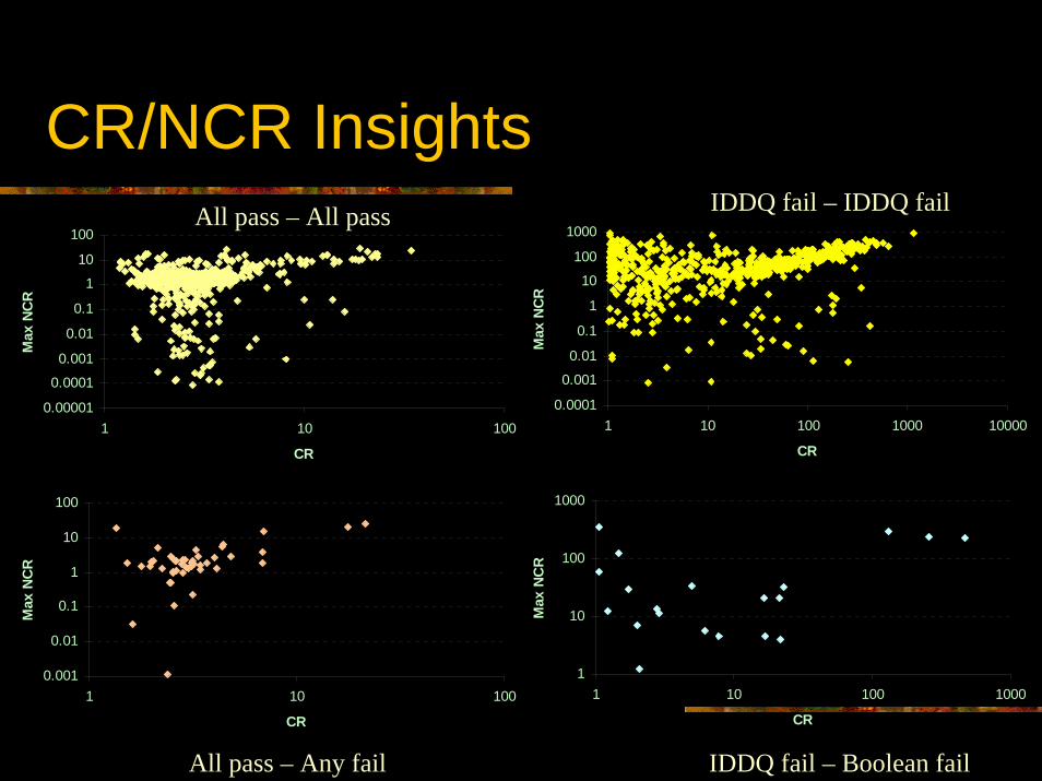
CR/NCR Insights
0.00001
0.00010.001
0.01
0.1
110
100
1 10 100
CR
Max
NCR
All pass – All pass
0.001
0.01
0.1
1
10
100
1 10 100
CR
Max
NCR
All pass – Any fail
0.0001
0.0010.01
0.1
1
10100
1000
1 10 100 1000 10000
CR
Max
NCR
IDDQ fail – IDDQ fail
1
10
100
1000
1 10 100 1000
CR
Max
NCR
IDDQ fail – Boolean fail

Healer Chips and CR/NCR! Healer – a chip that shows elevated IDDQ
before BI and reduced IDDQ after BI! Need more careful analysis
0.001
0.01
0.1
1
10
100
1000
1 10 100 1000
CR
Max
NCR

Immediate Neighbor Difference IDDQ Test (INDIT)! Ratios may pass some outliers
! Differences in IDDQ for same vectors ~ 0! Process variations cause variation
IND (i) = IDDQ Die 1 (i) IDDQ Die 2 (i)– ~ 0
Why Multi-parameter Test?
! IDDQ test alone not enough ! Pass/fail decision difficult and prone to error! Can result in yield loss/test escapes
! Need higher confidence in detecting flawed chips
! Defect detection capability diminishing for each test method in isolation! Defect detection harder with each technology node
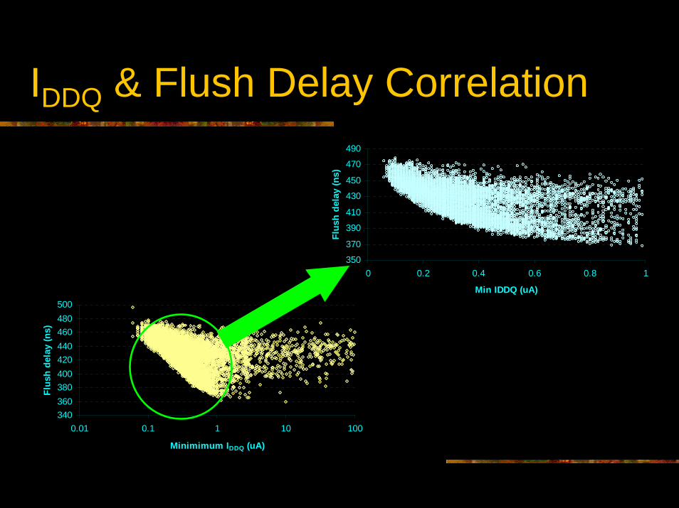
IDDQ & Flush Delay Correlation
340360380400420440460480500
0.01 0.1 1 10 100
Minimimum IDDQ (uA)
Flus
h de
lay
(ns)
350370
390410
430450
470490
0 0.2 0.4 0.6 0.8 1
Min IDDQ (uA)
Flus
h de
lay
(ns)
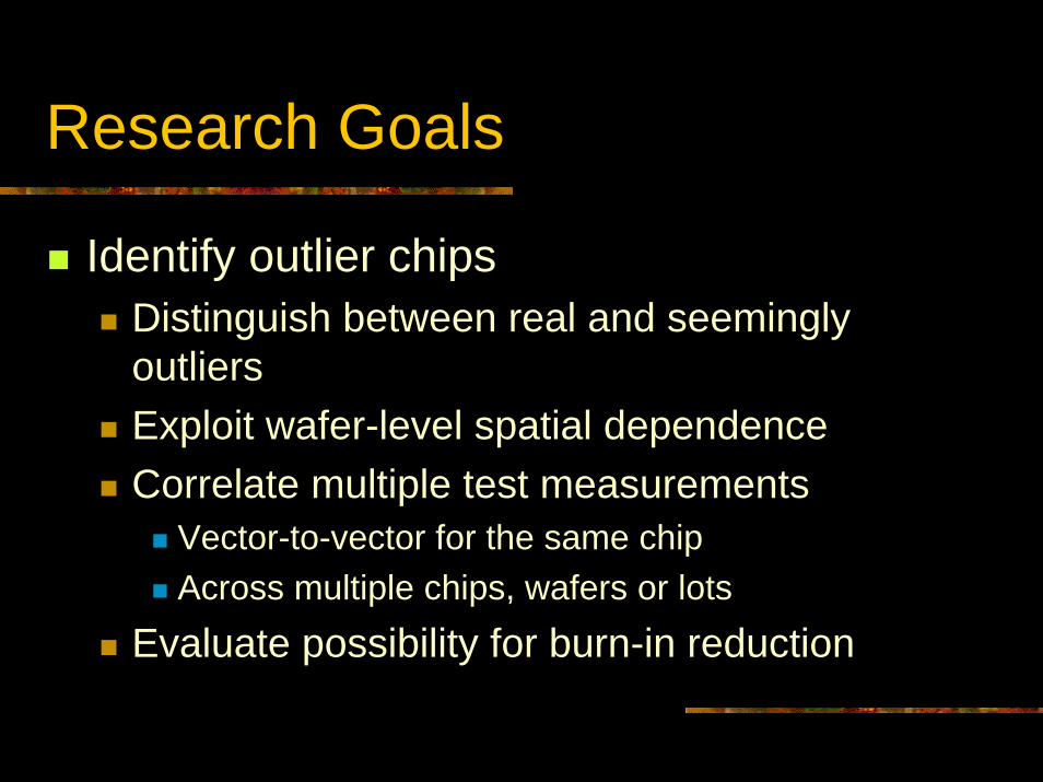
Research Goals
! Identify outlier chips! Distinguish between real and seemingly
outliers! Exploit wafer-level spatial dependence! Correlate multiple test measurements
! Vector-to-vector for the same chip! Across multiple chips, wafers or lots
! Evaluate possibility for burn-in reduction

Research Plan - I
! Extensive analysis of SEMATECH data! Evaluate different ideas! Correlate with BI results to validate methods! Data rather outdated (0.6 micron)
! Recent data obtained from LSI Logic! No BI data available! How to validate methods?
! Proposal sent to Texas Instruments! Discussed with Philips, IBM, Sony
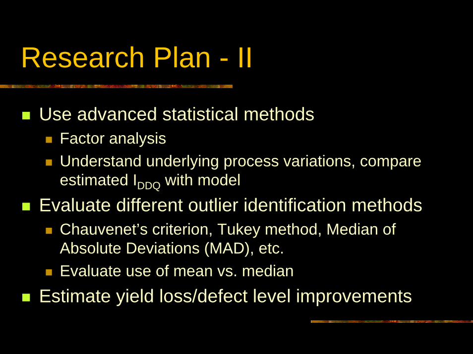
Research Plan - II
! Use advanced statistical methods! Factor analysis! Understand underlying process variations, compare
estimated IDDQ with model! Evaluate different outlier identification methods
! Chauvenet’s criterion, Tukey method, Median of Absolute Deviations (MAD), etc.
! Evaluate use of mean vs. median! Estimate yield loss/defect level improvements

Research Contributions
! Systematic identification of outlier chips! Neighboring chips’ parameter-based
estimation and statistical analysis for defective chip screening
! Insight into underlying process variations! Possible burn-in reduction or elimination
! Test cost reduction
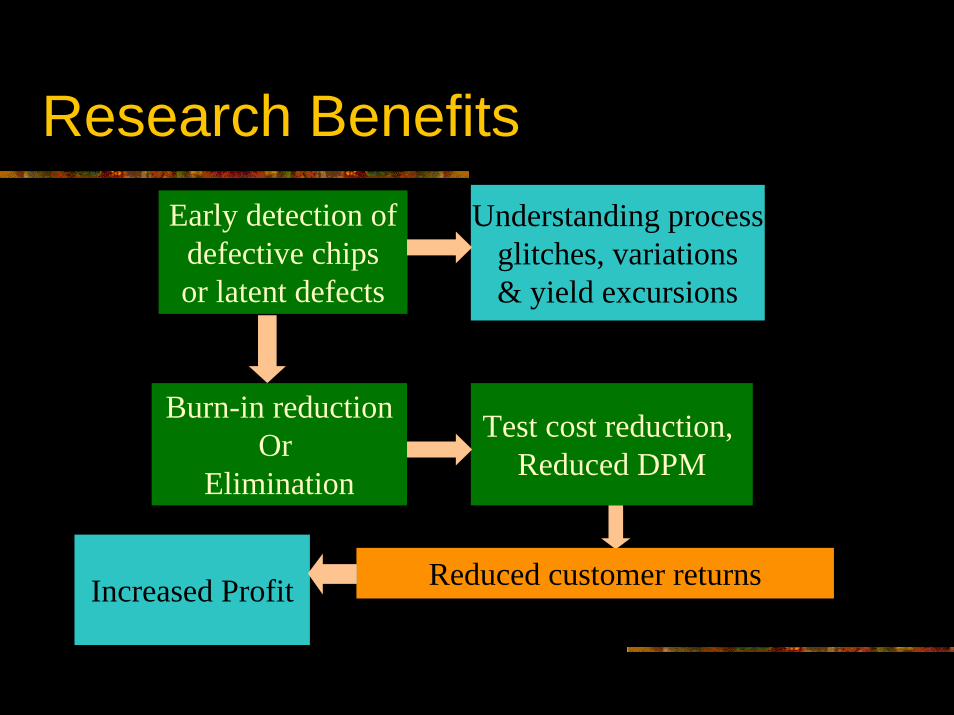
Research BenefitsUnderstanding process
glitches, variations& yield excursions
Early detection ofdefective chipsor latent defects
Test cost reduction, Reduced DPM
Burn-in reductionOr
Elimination
Reduced customer returnsIncreased Profit
Summary
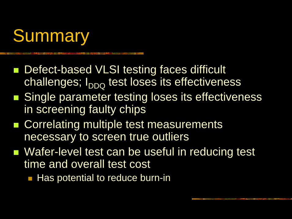
! Defect-based VLSI testing faces difficult challenges; IDDQ test loses its effectiveness
! Single parameter testing loses its effectiveness in screening faulty chips
! Correlating multiple test measurements necessary to screen true outliers
! Wafer-level test can be useful in reducing test time and overall test cost! Has potential to reduce burn-in

Questions?

Backup Slides
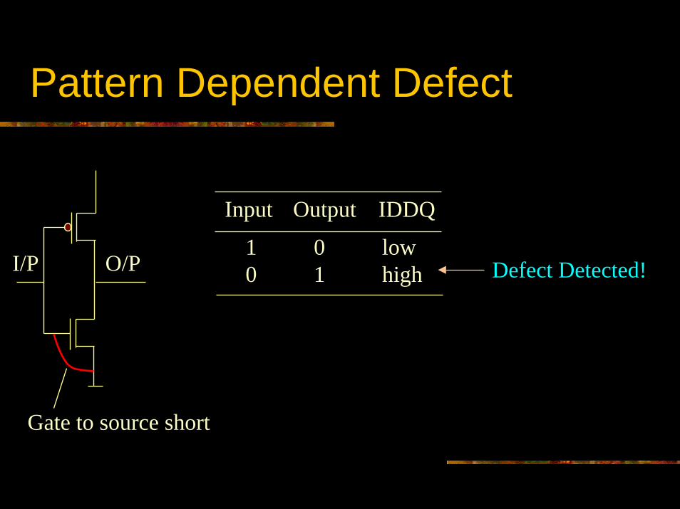
Pattern Dependent Defect
Input Output IDDQ
1 0 low0 1 highI/P O/P Defect Detected!
Gate to source short
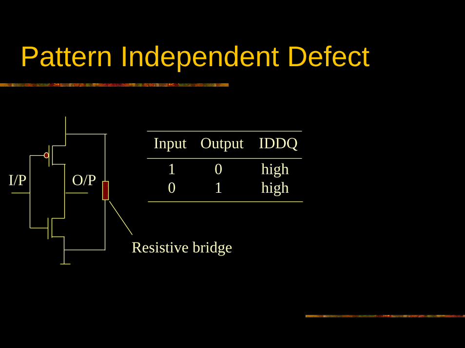
Pattern Independent Defect
Input Output IDDQ
O/P1 0 high0 1 highI/P
Resistive bridge

Short Channel Effect
Gate Length (um)
Vth
Gate begins to loseControl over the channelEffective Vth reduced(Vt Roll-off)
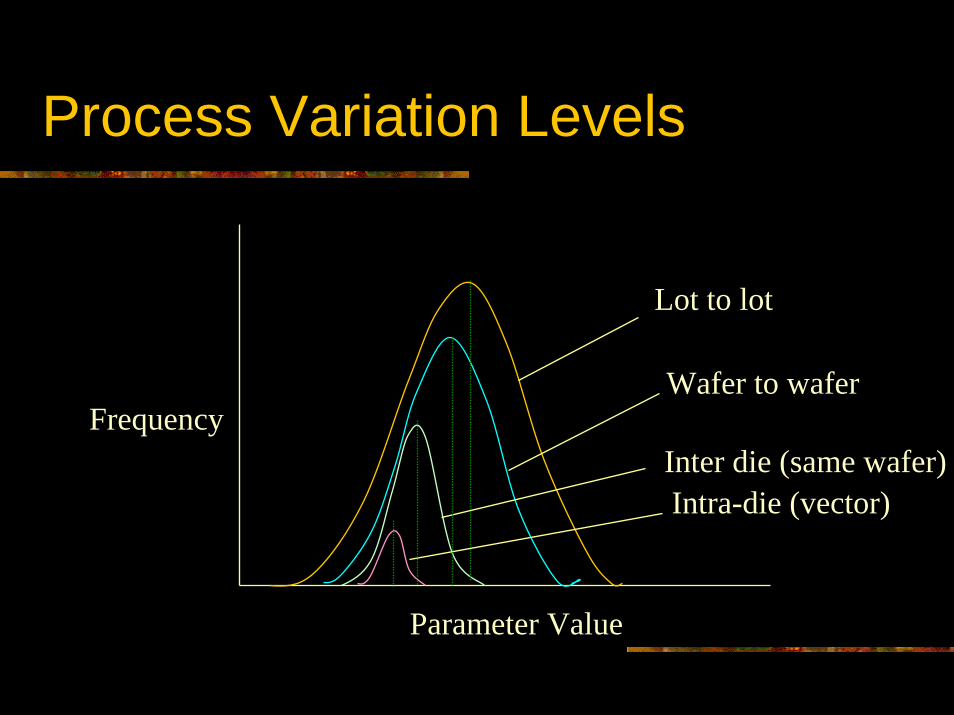
Process Variation Levels
Lot to lot
Wafer to waferFrequency
Intra-die (vector)Inter die (same wafer)
Parameter Value
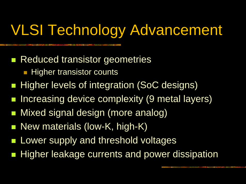
VLSI Technology Advancement
! Reduced transistor geometries! Higher transistor counts
! Higher levels of integration (SoC designs)! Increasing device complexity (9 metal layers)! Mixed signal design (more analog)! New materials (low-K, high-K)! Lower supply and threshold voltages! Higher leakage currents and power dissipation

Technology Impact on Testing! Reduced transistor geometries
! Increased process variations! New defect mechanisms
! Inaccurate fault models! Higher levels of integration
! Reduced observability and controllability of defects! Higher leakage currents
! Unable to distinguish faulty currents! Reduced voltage, increased temperature
! Reduced effectiveness of reliability screens

Impact on IDDQ Testing ! Reduced transistor geometries
! Reduced supply voltages to avoid gate oxide breakdown
! Necessary to reduce threshold voltage for performance requirements
! Increases leakage current exponentially! Cannot distinguish between faulty and fault-free
leakage currents using a single threshold! Unacceptable yield loss and/or test escapes
! Large process variations make it worse!

Scaling Implications on IOFFITRS Projections for High-performance Microprocessors
IOFF(nA/um)
Target Supply Voltage (VDD)
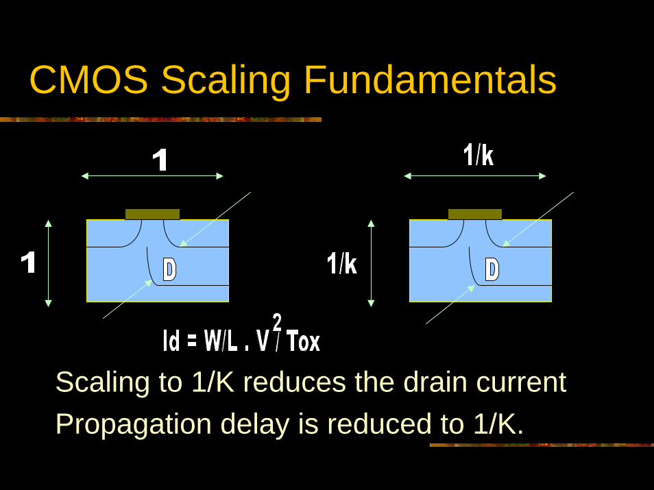
CMOS Scaling Fundamentals
Scaling to 1/K reduces the drain currentPropagation delay is reduced to 1/K.

Non-uniform Scaling Trends
! Tox scales faster than VDD
! Increased electrical field
! Performance depends on VDD-Vt
! Vt scales slower than VDD due to Boltzmann statistics
Source : ITRS 2001
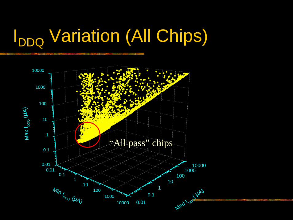
IDDQ Variation (All Chips)
0.010.1
110
1001000
10000
0.01
0.1
1
10
100
1000
10000
0.010.1
110
1001000
10000
Max
I DD
Q (µ
A)
Med I DDQ( µA)Min I
DDQ (µA)
“All pass” chips
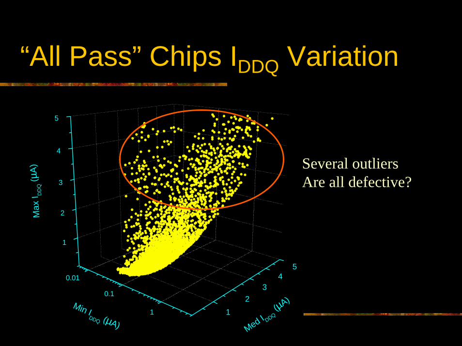
“All Pass” Chips IDDQ Variation
0.01
0.1
1
1
2
3
4
5
12
34
5
Max
I DD
Q (µ
A)
Med I DDQ (µA)Min I
DDQ (µA)
Several outliersAre all defective?
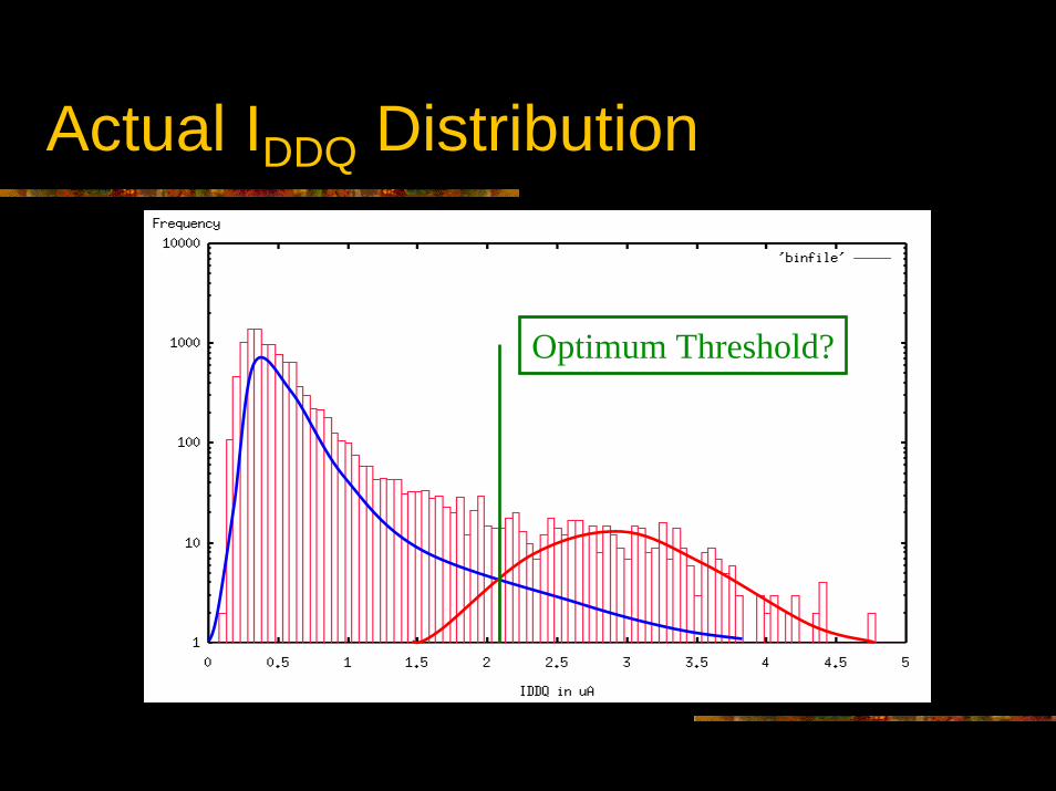
Actual IDDQ Distribution
Optimum Threshold?

Leakage Current ComponentsOutput = 0Input = 1
VDD
P+ substrateN-well
P+ P+ P+n+ n+ n+
IG
IDW
Reverse biased PN junction leakage
ID
IDS
Subthreshold current (weak inversion)
IGIDL
Gate Induced Drain Leakage (GIDL)
IPT
Punch-through Leakage
IDIBL
Drain Induced Barrier Lowering (DIBL)
Tunneling leakage through gate oxide

Leakage Current ComponentsOutput = 1Input = 0
VDD
P+ substrateN-well
P+ P+ P+n+ n+ n+
IDW
Reverse biased PN-junction leakage
IDS
IG
Gate Induced Drain Leakage (GIDL)
ID
Drain Induced Barrier Lowering (DIBL)
Tunneling leakage
Subthreshold leakage
Punch-through leakage
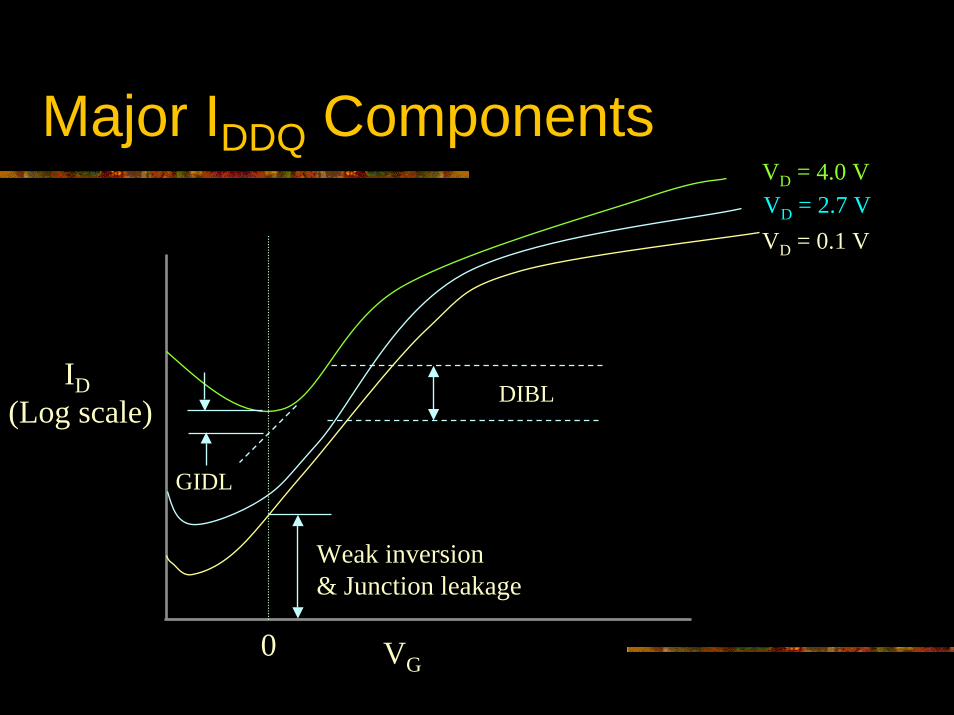
Major IDDQ Components
GIDL
Weak inversion& Junction leakage
DIBLID
(Log scale)
VD = 2.7 VVD = 4.0 V
VD = 0.1 V
0 VG

Do We Need a Smart Tester?
! “Automatic Test Equipment (ATE) is a misnomer. It should be called Automatic Measuring Equipment (AME). …We need statistical methods to discriminate faulty chips [from fault-free ones].”
- Robert Madge (LSI Logic) at Industrial Test Challenges talk at Intel in May 2002

Two Signature Types
0 50 100 150 20050.5
51.0
51.5
52.0
52.5
53.0
53.5
54.0
54.5
IDD
Q (
uA)
Number
Pattern Dependent Current Signature
0 50 100 150 2000123456789
101112131415
IDD
Q (u
A)
Number
Pattern IndependentCurrent Signature(Background leakage)
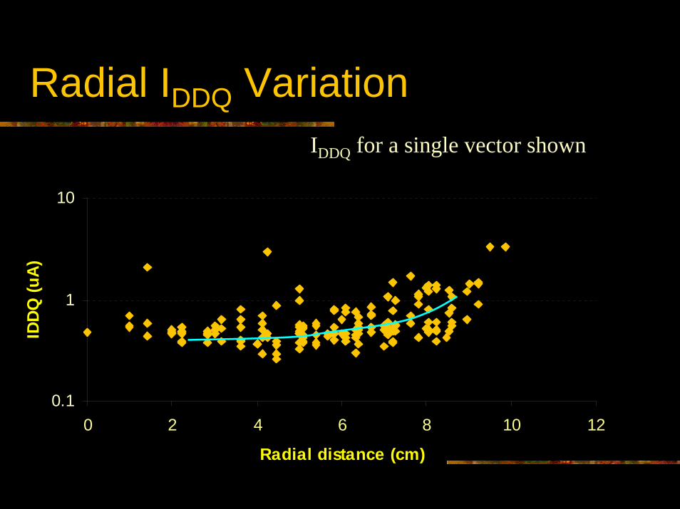
Radial IDDQ VariationIDDQ for a single vector shown
0.1
1
10
0 2 4 6 8 10 12
Radial distance (cm)
IDDQ
(uA)
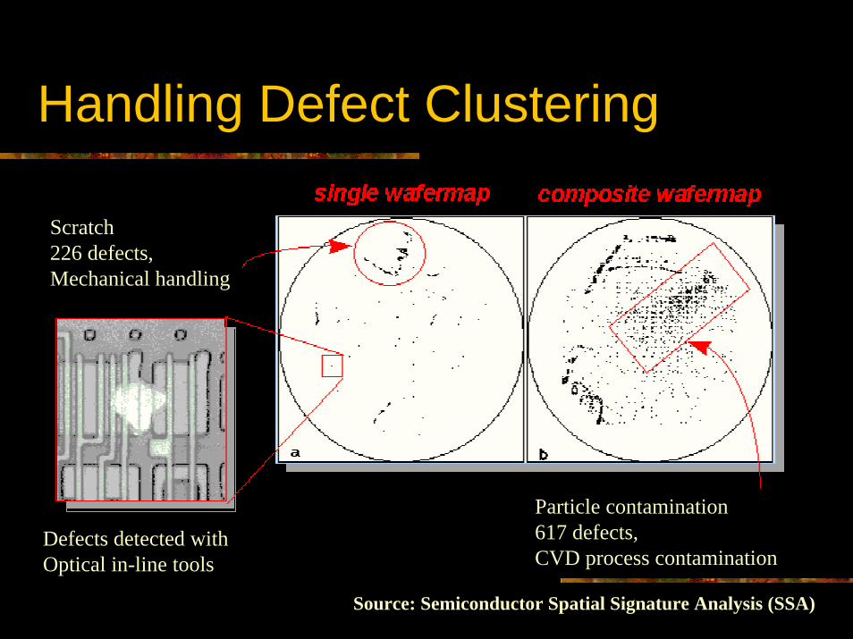
Handling Defect Clustering
Particle contamination617 defects, CVD process contamination
Scratch226 defects,Mechanical handling
Defects detected withOptical in-line tools
Source: Semiconductor Spatial Signature Analysis (SSA)

Correlation: What Does It Mean?
A
B
Positive correlation
A
B
Negative correlation
A
B
No correlation
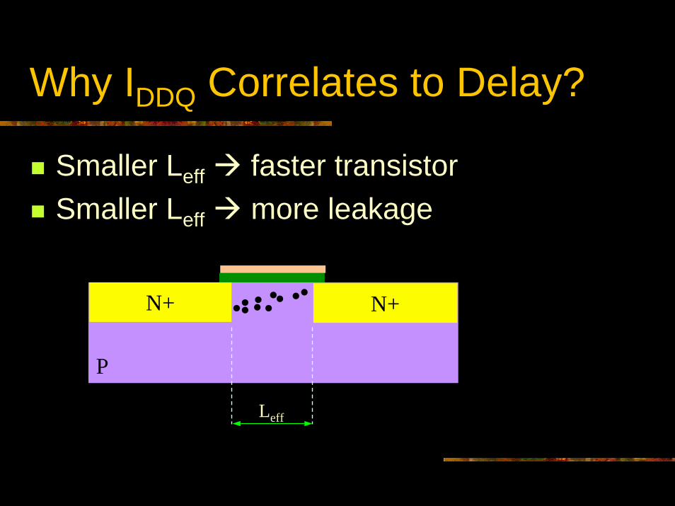
Why IDDQ Correlates to Delay?
! Smaller Leff " faster transistor! Smaller Leff " more leakage
N+ N+
Leff
P

How Reverse Body Bias Works?
! Reverse potential applied to substrate increases effective Vth
! This reduces leakage current! Penalty " switching speed reduces
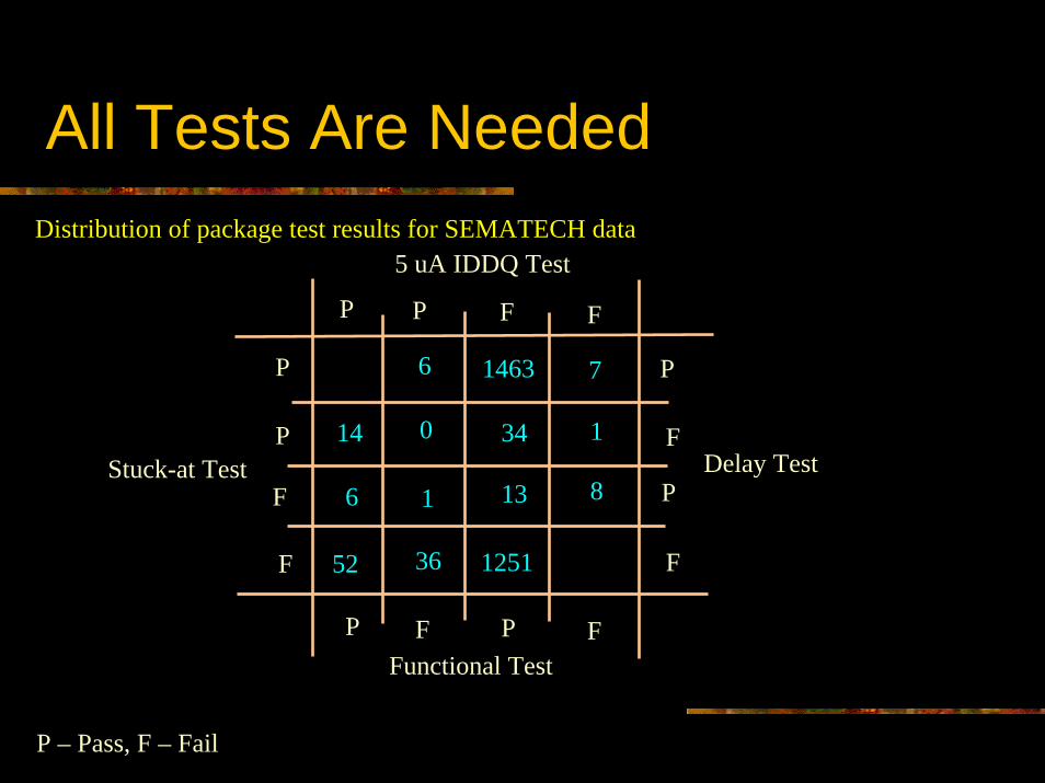
All Tests Are Needed
5 uA IDDQ Test
Delay TestStuck-at Test
Functional TestP P
P P
P
P
P
P
F
F
F F
F F
F
F
6 1463 7
14 0 34 1
6 1 13 8
52 36 1251
Distribution of package test results for SEMATECH data
P – Pass, F – Fail

Is IDDQ Irreplaceable?
2467 42
23 121
343 98
34
65
3573
1545 46
3118
+ 56 fail only IDDQ + AC scan+ 4 only functional + stuck-at
Wafer Test
521 19
25 25
124
48
86
31
46
6
7
+ 36 fail only IDDQ + AC scan
Package Test
IDDQ IDDQAt-speed Functional
At-speed Functional
Stuck-atScan
Stuck-atScan
AC scan
AC scan
150000 die at wafer, 76000 dice after package, package values normalized to wafer good partsSource: Peter Maxwell, Talk at Industrial Test Challenges, May 2002.

Fewer Vectors,Higher Coverage
FC byfunctional tests
FC byIDDQ tests
100
90
80
Fault Coverage %
70
60
50
40
30
20
10
Vector Number
For same FC IDDQ tests require many fewer vectors than functional test

Optimum Threshold Selection! Cost vs. Quality debate
Freq
uenc
y Zero Yield LossOptimum Threshold
High Overkill
Zero Test Escapes
HighDefect Level
Fault-free chips
Faulty chips
IDDQ

Wafer-level Analysis: Advantages
! Detection of defective chips at wafer probe! Reduction in test costs and time ! Reduced packaging cost/die
! Provides insight into understanding underlying process variations! Useful for detecting process glitches
! Different pass/fail criterion for different wafers! Reduce yield penalty for fast and leaky wafers

Values on Logarithmic Scale
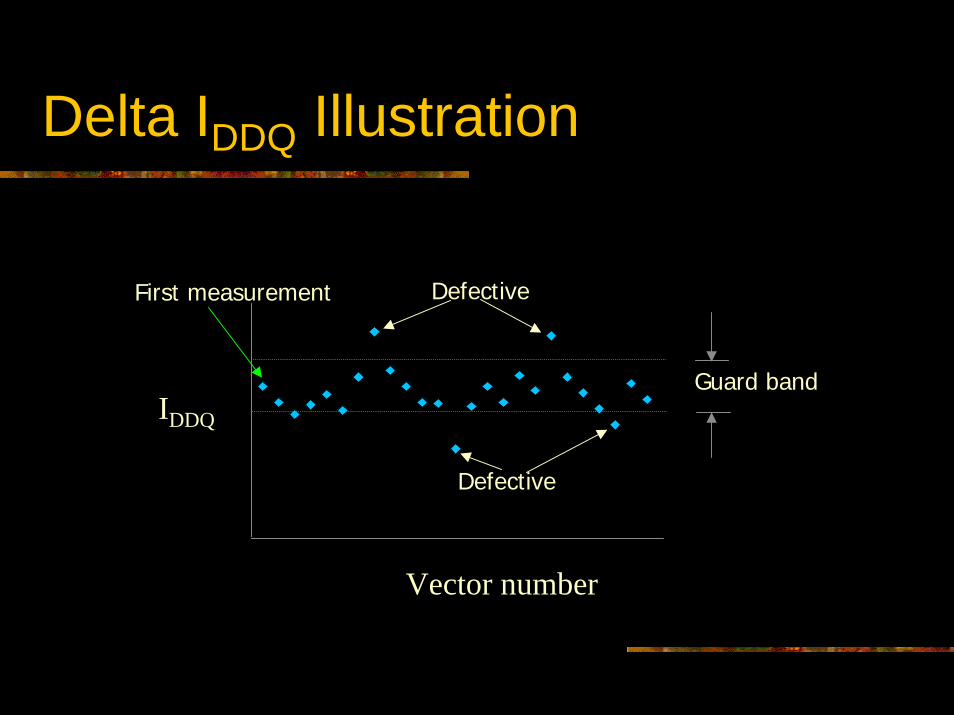
Delta IDDQ Illustration
First measurement
Guard band
Defective
Defective
IDDQ
Vector number
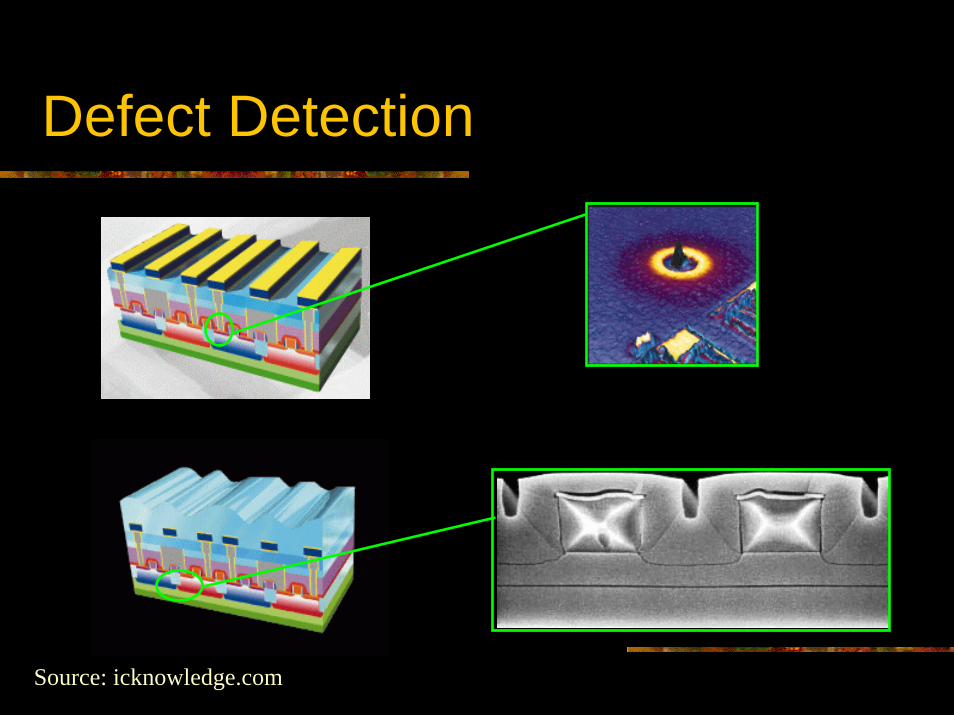
Defect Detection
Source: icknowledge.com
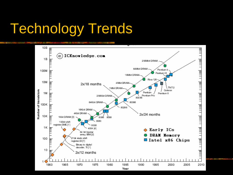
Technology Trends

IDDQ Test for Deep Sub-Micron! Yield loss and test escapes inevitable
Ith
IDDQ
Fault-freechips
Faulty chipsFr
eque
ncy
DSM Technologies
Test Escapes Yield Loss
IthFault-free chips
Freq
uenc
y
Faulty chips
IDDQ
Earlier Technologies


![How to zig when everyone else is zagging [SLIDEDECK]](https://img.dokumen.tips/doc/110x75/55a4f5441a28ab2e188b47ee/how-to-zig-when-everyone-else-is-zagging-slidedeck.jpg)


