Embed Size (px)
Citation preview

Research ArticleDesign and Analysis of a Low Cost Wave Generator Based onDirect Digital Synthesis
Jian Qi1 Qun Sun1 Xiaoliang Wu2 Chong Wang1 and Linlin Chen1
1School of Mechanical amp Automotive Engineering Liaocheng University Liaocheng 252059 China2Department of Medical Equipment Liaocheng Peoplersquos Hospital Liaocheng 252000 China
Correspondence should be addressed to Qun Sun sunxiaoqun97163com
Received 1 May 2015 Revised 6 August 2015 Accepted 6 August 2015
Academic Editor Raj Senani
Copyright copy 2015 Jian Qi et al This is an open access article distributed under the Creative Commons Attribution License whichpermits unrestricted use distribution and reproduction in any medium provided the original work is properly cited
Signal generators are widely used in experimental courses of universities However most of the commercial tests signal generatorsare expensive and bulky In addition a majority of them are in a fixed working mode with many little-used signals In order toimprove this situation a small sized and highly accurate economic signal generator based on DDS technology has been developedwhich is capable of providing wave signals commonly used in experiments Firstly it is introduced the basic principles of DDSand is determined the overall scheme of the signal generator Then it proposes a design of the hardware which include powersupply module display module keyboard module waveform generating module based on DDS chip and the minimum systemmodule based on C8051F010 The signal generator was designed to output sine and square waveforms and the other achievedperformances included the frequency range 01 Hzndash125MHz the frequency resolution 005Hzndash01 Hz the output amplitude 10ndash45 V the frequency accuracy 119870119891min = 9412 and 119870119891max = 9999 and the signal distortion 119877THDmin = 0638 and 119877THDmax =
1167
1 Introduction
Signal generators are widely utilized in experimental courses[1ndash8] Furthermore square wave and sine wave signalsgenerated by signal generators are extensively used in a widerange of applications usually as a standard signal in electroniccircuit testing parameter measurement or demonstrationin experimental courses However due to the high costfixed working mode and poor extensibility combine theprogrammable functions for generating arbitrary waveformsand other functions cannot be fully played out in the teachingexperiments of common signal generator a cheap and smallsignal generator which canmeet common signal output func-tions and be suitable for experimental courses was needed [9ndash12] Based on DDS technology an economic signal generatorwith small size and high precision was developed Squarewave signalwith tunable frequency pulsewidth and durationand high precision sine signal with adjustable amplitudeand frequency can be produced to satisfy the requirementsin teaching experiments Some reports focus on developingsignal generator by DDS technology in theory There are still
few reports about manufacturing of the signal generator byDDS technology
2 The Overall Design Scheme ofthe Signal Generator
21 Basic Principle of DDS Technology The basic principleof DDS is using the phase concept to carry out frequencysynthesis [2] which allows signals changing with phaseto be obtained according to the variation of given signalsunder different amplitude Phase accumulator is formed bycascaded 119873-bit adder with 119873-bit accumulator register Foreach arriving clock pulse 119891MCLK the adder sums up thecontrol word (119872) with the accumulated phase data producedby the phase accumulator register and the result is sentback to the input port of the accumulator register so thatthe adder continuously sums up the frequency control wordunder the effect of the subsequent clock pulse The phaseadder continuously performs linear adding of the frequencycontrol word in an accumulative fashion under the effect of
Hindawi Publishing CorporationJournal of Electrical and Computer EngineeringVolume 2015 Article ID 367302 17 pageshttpdxdoiorg1011552015367302
2 Journal of Electrical and Computer Engineering
2568
12
16
20
24
28
32
48
4096
65536
1048576
16777216
268435456
4294967296
281474976710656
N
0000 0
1111 1
M
Figure 1 Diagrammatic sketch of the operating principle of phaseaccumulator
the clock input As shown in Figure 1 a sine wave is regardedas oscillation of a phase cycle in a rotating vector mannerand each given point on the phase wheel corresponds to anangular division point on a sine wave in a 0sim2120587 cycle Everytime a vector turns around a phase circle at a constant speeda complete cycle of sine wave is produced It can be seen thatthe phase accumulator adds the control word once followingeach clock input the output data of the phase accumulator isthe phase of the synthesized signal and the output frequencyof the phase accumulator is the signal frequency of the DDSoutput The frequency control word determines the numberof division points that can jump on the phase cycle in eachtime clock cycle More division points lead to faster overflowof the phase accumulator and shorter time to complete equalsine wave cycles thus changing the value of the control word(119872) can alter the output frequency [4]The output data of thephase accumulator serves as the phase sampling address of awaveformmemory (ROM) A phaseamplitude conversion iscompleted after retrieving the binarywaveform sample valuesstored in the waveform memory using a lookup table
22 The Overall Program Design of Signal Generator Thefunctional structure of the signal generator block diagram asshown in Figure 2 mainly consists of a power supply system
LCD SDATA
MCU
KEY SCLK
SDATADDS
AD9833
DA
Mul
tiplie
r
Comparative shaping
Relay
Sinusoidalwave output
Square wave output
Sinusoidal and square control signal
Wave output
Figure 2 Block diagram of the signal generator based on DDS
SCM system DDS waveform generator module amplitudeadjustment module square wave generator module relayoutput module and so onThe power supply system provides25 V 33 V plusmn5V and plusmn15 V power supply voltage The +5Vinput of the power supply system goes through an integratedthree-terminal voltage regulator to obtain 25 V and 33 Vvoltage and then uses a DC-DC power supply module forconversion to +5V and +15V The SCM system is employedto control the operation of the human-machine interfaceread keyboard display on LCD and adjust the output sinewave amplitude It also undertakes programming of the DDSdevice to produce the corresponding frequency signal tocontrol the relays and switch sine and square wave outputs
3 Hardware Design of the Signal Generator
31 Design of the Power Supply Circuit As shown in Figure 3the inputs and outputs of AS1117-25 AS1117-33 and the DC-DC module use 330 120583F and 01 120583F capacitors for frequencycompensation to prevent the regulator from generatinghigh-frequency self-excited oscillation and to suppress high-frequency interference in the circuit The output terminalsof the A05S05-2W and A05S15-1W power modules haveresistors and capacitors to form a low-pass filter which cansmooth power output spikes and reduce interference to thesubsequent circuit chip The reverse protection design is alsoused in the power supply circuit where a diode D3 is incut-off state under normal power supply If the input voltageis reversed the diode conducts and the current from theexternal power supply flows through the FUSE and diodeD3 into the negative terminal of the power supply Since thediode forward resistance is very small the current increasessharply and burns out the FUSE disconnects the circuit andthus protects the internal circuit from being damaged
32 Design of LCDModule The liquid crystal displaymodulewas built on LCM1602 that has 2 times 16 characters andinternal font The interface is shown in Figure 4 where 11987712
Journal of Electrical and Computer Engineering 3
AVCC +33
DVCC +33
AVCC +15
C34
DVCC +5
RS
5
T13
Phonejack3
21
MHDR1X2
POW5V
C24
Cap Pol1
Cap Pol1 C31
C25Cap
C32Cap
D3
Dio
de 1
N40
07
C33Cap Cap
C29Cap
C30Cap
470Res2
470Res2
AVCC +5
C28C27Cap Cap
C19Cap
C20Cap
10Res2
10Res2
20Res2 C14
CapC15
Cap
500Res2
LED
GN
D1
2AS33
AS1117
3
GN
D1
23AS25
AS1117C38
Cap Pol1C39Cap
C18
Cap Pol1C21Cap
20Res2
C16Cap
C17Cap
20Res2
C22Cap
C23Cap
20 Res2C35CapC37Cap
C36Cap
C26Cap
FUSE
Fuse 1
1
GND24
5
6A0505
A05
1
GND24
5
6A0515
A05
Vin+
Vin+
Vin Vout
Vin Vout
+Vo
minusVo
+Vo
minusVoAVCC minus15
AVCC minus5
PLUGEin +5V
01 120583F
01 120583F 01 120583F
01 120583F
01 120583F
01 120583F
01 120583F01 120583F
01 120583F
01 120583F
01 120583F
01 120583F
47 120583F
47 120583F
INPUT +5V
INPUT +5V
INPUT +5V
+
+
+
+
470120583F
470120583F15120583F
15120583F
1120583F
1120583F
1120583F
1120583F
1120583F
1120583F
1120583F
1120583FVREF0
R21
R19
R24
R23
R22
R20
R18
R16
R17
0V
0V
Figure 3 Circuit of the power supply
potentiometer can be used to adjust the potential of feet 3 tochange the contrast of the LCD display
33 Design of Keyboard Circuit The front panel of the signalgenerator is shown in Figure 5 By means of pressing the leftor right buttons to select each bit of data to be transferred andthen using add or subtract settings the number of buttonscan be reduced and remained the same when the data fortransmission needs to be extended This allows the circuitto be very flexible since appropriate changes can be made inthe software The circuit output functions can be selected byldquosinesquare waverdquo buttons The output signal frequency canbe configured under a square wave output state whilst for asine wave output state the signal frequency or amplitude canbe set or modified through the ldquoModerdquo button
As shown in Figure 6 the ldquosinesquare waverdquo is designedwith a locking switch whilst the ldquoAddrdquo ldquoReducerdquo ldquoShiftleftrdquo ldquoShift rightrdquo and ldquoModerdquo buttons are designed withoutlocking switchThe output is high level 33 Vwhen SW1simSW5are released and low level when pressing themWhen Switch6is released PIN2 connects to PIN3 and PIN5 connects toPIN6 while PIN1 is hanging SINREC is high level andLED SIN lights up indicating the output is sine wave Whenit is pressed SINREC is low level and PIN4 connects toPIN6 and LED REC lights up showing the output is squaredwave signals
34 The Circuit Design of Wave Generator
341 The Circuit Design of Sine Wave Generator As is shownin Figure 7 the signal generator is based on a DDS chip
4 Journal of Electrical and Computer Engineering
RS
RSRPot
LCD
GND[10]AGND
RW
RW
E
E
123456789
10111213141516
D0D1D2D3D4D5D6D7
D0D1D2D3D4D5D6D7
LCD[100]
AVCC +5
AVCC +5
MHDR1X16
AVCC +5
10k
R12
VCC[70]
Figure 4 The interface circuit of LCD
+ minus larr rarr M
Add Reduce Shift left Shift right Mode Sinesquare wave
Figure 5 The shifting keyboard panel design
AD9833 made by Analog Devices Inc (ADI) which is25MHz with active crystal as a reference clock
342 Design of the Sine Wave Amplitude Modulation CircuitAccording to the required sinusoidal amplitude which isinput by the keyboard the DA port of the microcontrollerproduces a corresponding DC signal then feeds it to themultiplier and multiplies it with a fixed amplitude sinusoidalsignal to achieve the function of regulating the amplitude asshown in Figure 8
The multiplier is selected to be MPY634 which ispowered by plusmn15 V voltage and can adopt a single-endedinput (plusmn10V) or a differential input (plusmn11 V) while the outputvoltage can reach plusmn11 V The relation of output voltage andinput voltage is given by
119881out = 119860((1199091 minus 1199092) (1199101 minus 1199102)
SFminus (1198851 minus 1198852)) (1)
Since the multiplier has internal negative feedback and119881out is limited the amplification factor (119860) is infinite in theoryand is at least 85 dB in practice therefore
(1199091 minus 1199092) (1199101 minus 1199102)
SFminus (1198851 minus 1198852) = 0 (2)
The sinusoidal wave amplitude ranges from 0038V to0650V thus the DC component (119881119900) is 0344V The outputfrom the multiplier must be the sine wave without DCcomponent so the DC component should be subtractedusing circuit shown in Figure 8 The resistor 11987727 is linked
between port 1198851 and port OUT and resistor 11987726 is linkedbetween ports 1198851 and 1198852
Assuming the resistances of 11987726 and 11987727 are 119909 and 119910 then
1198851 minus 1198852 = 1198811015840out lowast
119910
119909 + 119910 (3)
1198811015840out is the output voltage of multiplier and the following
can be concluded
(1199091 minus 1199092) (1199101 minus 1199102)
SF= 1198811015840out lowast
119910
119909 + 119910 (4)
Therefore
1198811015840out =
119909 + 119910
119910lowast(1199091 minus 1199092) (1199101 minus 1199102)
SF (5)
Assuming that
1198700 =119909 + 119910
119910lowast
1
SF (6)
1198700 is the gain of the multiplier of the two differentialinputs
1198811015840out = 1198700 lowast (1199091 minus 1199092) (1199101 minus 1199102) (7)
The current of the multiplier output cannot outputdirectly because of its weakness of driving power so a highspeed operational amplifier must be set before the input ofthe multiplier to increase the output current
Journal of Electrical and Computer Engineering 5
SW-PB
SW-PB
SW-PB
SW-PB
SW-PB
10k10k10k10k10k10k
SW1AGND
AGND
Switch
2
3
1
5
6
4
Res2 Res2LED1
Switch
LED2
Res2 Res2 Res2 Res2 Res2 Res2
Res2
Res2 500
500
Left
Left
Right
Right
Up
Up
Down
DownMode
Mode
SINREC
SINREC
SW2
SW3
SW4
SW5
AVCC +33
AVCC +33
AVCC +5
AVCC +5
KEY[50]
GND[10]
LED_REC
LED_SIN
130k 130k
VCC[70]
R6R5R4
R36R35R14
R15
R3R2R1
Figure 6 The keyboard circuit
41 GND 2
CLK 3
ATXL
CLOCKDVCC +5
C5
Cap
1 OEA12 18A24 16A36 14A48 12
MC74HC244AN
DGNDDRIVEA
C1Cap
C3Cap C2
CapAVCC +5
AVCC +5C4
Cap
DDS_SINOUT
SCLKSDATAFSYNC
COMP 1
2
CAP
3D
GN
D4
MCLK5
67
8
AGN
D
SCLKSDATAFSYNC
9
10
AD9833
GND
OUT
DGND
SCLKSDATAFSYNC
AVCC +5DVCC +5
AGND
DDS[20]
01 120583F
001120583F
01 120583F
Vout
10120583F
VCC[20]VCC
VD
D
GND[10]
Y1Y2
Y4Y3
Figure 7 The circuit of wave generator
2
SF 467
8
1011
OUT 12+V 141
NC 3
NC 9NC 5
NC 13
MPY
MPY634KPCapC8
C7AVCC +15
DAC0Cap
MPY_SINOUTDDS_SINOUT12 NC
+In34 5NC
6+VS 7NC 8Res2AD8061
AVCC +5AMP_SINOUT
RPot C44Cap
C45Cap
Res2
Res2
Res2
Res2
Y2Res2
Res2X
Y
10 k
10 k
1k
2k
minusIn
minusVS
Vminus
4k
1k
Vout
01 120583F
01 120583F
01 120583F 01 120583FAVCC minus15
AVCC minus5Vout
VRE
F0
136k
R28
R29
R31
R32
R27
R26
R30
R8
Y1Y2
X1X2
Z1Z1
Z2 Z1
Figure 8 The circuit of regulating the sinusoidal amplitude
6 Journal of Electrical and Computer Engineering
GND
GND
3
1
2
+0344V
+5V
AS1117-25
R1
R2
R3
+25V
Figure 9 The circuit of offset voltage of the amplifier
Taking 11987730 = 2KΩ 11987731 = 1KΩ 11987732 = 1KΩ the ampli-fier multiple is 119860 = 1 + 1198773111987730 = 3 then
119881out = 3 lowast 1198811015840out = 31198700 lowast (1199091 minus 1199092) (1199101 minus 1199102) (8)
The output voltage of DAC of the MCU is ranging from 0to 24V and the sinusoidal waveform of DDS is ranging from0 to 065V so theDC component of sinusoidal waveform (119881119900)is 0344V
Reducing the DC component at 119884 input of MPY634 theamplitude of sinusoidal waveform is
119881in = 119881dds minus 119881119900 = plusmn0306V (9)
Multiplying the two differential inputs 119883 and 119884 gives24 lowast 0306 = 07344 so it is required to get the amplitude ofsinusoidal waveformmore than 4V the gain must be chosenabove 407344 = 54
The way of the circuit connection decides the value of1SF
When Port SF is hanging the amplification factor is SF =10V which is accurately modified by laser in the integratedcircuit and the error is 01 or less
Through resistor 119877SF linking between PIN SF and PINminus119881119878 the value of SF can be changed
119877SF = 54 lowast (SF
10 minus SF) (10)
Defining 119909 = 136KΩ 119910 = 4KΩ then
119870 = 3 lowast 1198700 = 3 lowast119909 + 119910
119910lowast
1
SF= 105
119881out = 103 lowast (1199091 minus 1199092) (1199101 minus 1199102)
119881outMax = 10 lowast 24 lowast (plusmn0306) = plusmn73V
(11)
Because of the amplifier providing plusmn5V in practice theoutput voltage can only reach about plusmn45 V
The amplitude of sinusoidal waveform ranges from0038V to 0650V and its DC component is 0344V whichis obtained by resistor divider As shown in Figure 9 theAS1117-25 three-port voltage stabilizer provides the voltage of25 V providing the offset voltage of 0344V through resistordividing
Taking 1198771 = 60KΩ 1198772 = 10KΩ 1198773 = 10KΩ theoutput scope of reference voltage is
119881ref0min = 25 lowast1198773
1198771 + 1198772 + 1198773
= 03125V
119881ref0max = 25 lowast1198772 + 1198773
1198771 + 1198772 + 1198773
= 06250V(12)
Therefore the output scope of reference voltage rangesfrom 03125V to 06250V and it is possible through adjustingpotentiometer to get the offset voltage of 0344V Thereforeit is possible to eliminate the DC component of sinusoidalwaveform from DDS output Introducing a positive feedbackto the circuit constitutes a hysteresis comparator throughadding a branch of voltage divider from comparator outputto in-phase input This can be seen from the schematic inFigure 10(a)
When input voltage 119881119868 is gradually increased from zerobut is less than or equal to 119881119879 which is called ceiling triggerlevel 119881119900 = 119881
+om
119881119879 =1198771119881REF1198771 + 1198772
+1198772
1198771 + 1198772
119881+om (13)
When the input voltage 119881119868 is greater than 119881119879 119881119900 = 119881minusom
and the triggering level is changed into1198811015840119879 which is called thelower trigger level
1198811015840119879 =
1198771119881REF1198771 + 1198772
+1198772
1198771 + 1198772
119881minusom (14)
Journal of Electrical and Computer Engineering 7
Vi
Vref
R
Vo
R2
R1
(a) The schematic diagram of hysteresis comparator
Vo
Vt VsVt998400
(b) The voltage transmission characteristic of hystere-sis comparator
Figure 10 Principle of the hysteresis comparator
AGND
RELAY_OUT
AVCC +5
Res2
C10Cap
C12
AVCC +5
CMP_RECOUTIn+2
3
Vminus4 LE 5
GND 6Out 7Out 8
V+1
CMP
MAX9686
CMP_REF
RELAY0_OUT
Res2
0Res2
RPot
Res2
100 kRes2
AVCC minus5
AVCC minus5
GND[10]
Vin
Vout
Inminus
1k
1k
2k
01 120583F
01 120583F
20k
VCC[70]
R33
R34
R9
R13
R11
R10
Cap
VREFVREF
Figure 11 The circuit of generating square waveform
The threshold voltage is
Δ119881 = 119881119879 minus 1198811015840119879 =
1198772
1198771 + 1198772
119881+om minus
1198772
1198771 + 1198772
119881minusom
=1198772
1198771 + 1198772
(119881+om minus 119881
minusom)
(15)
From Figure 10(b) of voltage transmission characteristicsof the hysteresis comparator it can be seen that the compar-ison voltage is different between the direction of incrementand the direction in input voltage and the interference withinthe hysteresis range will not affect the output voltage
The circuit of generating square waveform is shown inFigure 11 Port 119881REF provides 25 V voltage for the voltageregulator module the voltage can be regulated by adjusting apotentiometer and the comparator outputs about 4V of highlevel So the backlash voltage of the circuit is
Δ119881 =1198779
11987733 + 1198779
(119881+om minus 119881
minusom) asymp 40mV (16)
35 The Design of Controlling Circuit of Relay Output Asshown in Figure 12 the relay module UA2 is equivalent toa double-pole double-throw switch The control sides PIN1
and PIN8 are respectively connected to the +5V supply andsinesquare waveform changeover switch PIN2 PIN3 PIN4are the switch for final wave output switching and PIN6PIN7 PIN8 are the switch for shifting sine wave to hysteresiscomparator to produce a square wave Diode D1 is for currentlimiting to prevent excessive current impact on the circuit
When the sinesquare waveform switch is releasedSINREC becomes high level and there is no current throughthe relay coil or the current is very small which means thatit does not produce magnetic force The connection of PIN6and PIN7 will put the sinusoidal signal into the comparatorto create square waveformThen the square signal will inputinto PIN2 of the decay which would sent to external interfacebecause of the connection of PIN2 and PIN3 When thesinesquare waveform switch is pressed SINREC changes tolow level thus the relay coil generates a magnetic force Theconnection of PIN5 and PIN6 separates the sine wave signalfrom the comparator to prevent generating interference Theconnected PIN4 and PIN3 deliver the sine signal generatedfrom the amplitude to the external output interface
36 The Design of MCU Controlling Circuit As shown inFigure 13 a CYGNAL C8051F series MCU was chosen to
8 Journal of Electrical and Computer Engineering
D1
Output
12
Header 2H
CMP_RECOUTAMP_SINOUT
AVCC +5SINREC 8
425 6
3
1
myRelay
Diode 1N4007RELAY0
RELA
Y0_O
UTAMP_SINOUT 7
AGND
AVCC +5
SINREC
VsinVrec
GND[10]
KEY[50]
VCC[70]
Figure 12 The circuit of relay controller
AGND56
1234
CP1+
CP0+
AIN078 AIN19 AIN210
1112
AIN3AIN4AIN513
14 AIN6AIN715 AGND16 AV+
AV+
17 20RS
T
XTA
L1XT
AL2
21TM
S22
TCK
23P3
324
P32
25 26 27P3
1P3
0P2
128
TDI
29TD
OD
GN
D30 32
P15
DVC
C +3
331
DG
ND P20 33
34P1435P13
P12P11 36P10P00
373839
DGND 40P01 42
43
41P27P26 44
45P3746P36
P02 47P03 48
P04
49P0
550
P25
51P2
4P2
3P2
25253
P06
54P0
755
P35
P34
5657P1
758
P16
59D
GN
D6061
DAC
0D
AC1
626364
C8051F000C8051F005C8051F010C8051F015
MCUC8051F0005_0105
13 4579
JTAG
Header 5X2
2
68
10
DVCC +33
TCKTDOTMS
TDI
DVCC +33
Res2
D1D0
D2D3D4
D5
D6
D7
A111 9A213 7A315 5A417 3
MC74HC244AN
DRIVEB19 OEDGND
8051_RS8051_E
8051_RW
RSE
RW
FSYNC
Left
Righ
tAVCC +33
TMS
RST
TCK
TDI
TDO
AVCC +33
DGND
DG
ND
DAC
0D
AC1
DVC
C +3
3
C11 Cap
C13Cap
C9
Cap
DVCC +33P00
CapC6
21
DDS_SINOUTMPY_SINOUTCMP_RECOUT
CMP_REF
P01
P02P03
CP0+
AIN0AIN1AIN2AIN3
SCLK
SDAT
AP0
7P0
6U
pD
own
Mod
eSI
NR
ECP0
5P0
4
AIN0AIN1AIN2AIN3
CP0+
P00P01P02P03P04P05
1 2XTAL
XT1A
L18 19
XT2A
L
C42
Cap
C41Cap
C40Cap
XTAL02
Res2
XTAL011 23 4
Header 2X2
XTAL01XTAL1
VERF
Header 2
XTAL_PINXTAL02XTAL2
1 23 45 67 89 10
11 1213 1415 16
TEST_PIN3
Header 8X2
P06P07 CP1+
CP1+
RESET
SW-PB
C43
DVCC +33
RST
4321
TEST_PIN2
Header 4
D0D1D2D3D4D5D6D7
RSRW
E
Left
UpRight
DownMode
RST
SINREC
RST
DAC12
DAC0DAC1
Header 2
DAC
CP1minus
CP1minus CP1minus
CP1minusCP1minus
CP0minus
51 k
KEY[50]
LCD[100]30pF
30pF30pF
01 120583F01 120583F
01 120583F
01 120583F
VDD
VD
D
VD
D
01 120583F
Cap10k
VREF1 VREF
VREF1
VREF0
R7
R25
Y1Y2
Y4
Y3
Figure 13 The controlling circuit of MCU
implement the functions of reading keyboard displayingLCD programming DDS chip and adjusting the amplitudeof the sinusoidal signal Considering the rules of microcon-troller pin configuration the internal digital resources startfrom P0 port therefore when assigning peripheral deviceport the MCU starts assigning from P3 port to reserve P0port for the internal resources
37 The Deployment of PCB and Anti-Interference DesignBecause of the hybrid-system of digital circuit and analogcircuit and its high operating frequency much attentionshould be put to the deployment of PCB and its anti-interference design Considering the cost and the size thePCB board is designed with double-layer plate and doublewiring Separate the digital circuit and analog circuit in PCB
Journal of Electrical and Computer Engineering 9
Crystal
GND
Figure 14 The PCB design diagram of AD9833
Figure 15 The whole PCB design diagram
layout and wiring In general we should adopt the way ofseparating digital signal ground with analog signal groundand connecting them at a point For the part of analog circuitwhich includes DDS chip multiplier and relay it shoulduse the way of linking grounds respectively and linking theground at a point thicken the ground line at the same time
The clock circuit of DDS wave generator is a critical partin the design which can be easily interfered and have greatinfluence on the quality of the output wave so we should payspecial attention to this part In order to reach the purpose ofisolation the crystal oscillator should be close to the pin ofDDS chip thicken the line of crystal oscillator and the poweradd cuprum to the shell of the crystal oscillator The PCBdesign diagram of AD9833 is shown in Figure 14
We should make the power line bold as large as possiblebecause of its high current and take the impedance intoconsideration The STAR structure is used in the powerwiring In fact in this design it is designed into the shorteststructure by manual wiring at first which must control thewidth of the conducting wire Then for each current channelof their device the conducting wire must guarantee morethan 20mils Finally the circuit will be fulfilled into STARstructure Finally fulfill the circuit into STAR structure Thewhole PCB design diagram is shown in Figure 15
4 The Software Design of Signal Generator
41 The Overall Design of Software The main programdiagram of SCM software is shown in Figure 16 which isbased on the idea of structured and modular design Theinitialization section mainly deals with writing operation ona few special function registers to set the mode and initialvalue of each module and initialize variables used Thenoutput the default waveform and restore the last workingstate if reset source is the watchdog or the missing clockdetector Scanning of the keyboard is controlled by timerT0 implemented into different subfunctions according todifferent waveforms and waveform generating mode
42 The Software Design of Signal Generator AD9833 is pro-grammable DDS signal generator with two 28-bit frequencyregisters inside and two 12-bit phase registers The softwareblock diagram is shown in Figure 17
Firstly write 16-bit operating mode command wordto determine working conditions and select the frequencyregister and phase register and secondly write one or twofrequency control words to control the output frequencyFinally write phase control word so that the DDS signal gen-erator can output waveforms corresponding to a frequencydetermined by the value of the frequency register and thephase determined by the value in the mode register Thesequence chart of data writing is shown in Figure 18
43 The Software Design of Keyboard Inputting The blockdiagram of keyboard scanning is as shown in Figure 19Use the 10ms interrupt of timer T0 to implement keyboardscanning and eliminate keyboard dither according to thenumber of interruption In the timer several operationsare governed such as mode switching data adding datareduction and left or right shift of data to be configured Indifferent modes the range of the input data can be limited toprevent the input out of range If no keyboard action can bedetected beyond seven seconds it will automatically exit theFM or AMmode and return to normal waveform generationstatus
44 The Software Design of LCD Displaying
441 The State of Sine Condition In different modes theLCD must display different interface for the user If itis the normal sinusoidal waveform generation mode asdemonstrated in Figures 20(a) and 21(a) then turn off theLCD blinking of cursor and character display the currentamplitude in the first line and show current frequency in thesecond line The high bit 0 is not displayed If it is sinusoidalFM mode as shown in Figures 20(b) and 21(b) set thecharacter and cursor to blink and adjust the lowest bit bydefault and adjust the cursor by the left and right keys Thelowest bit to the right will move the cursor to the highestlevel and the highest bit to the left will move the cursor tothe lowest position The data size is changed by the Add andSubtract keys if the most significant bit to adjust the data sizeis limited to be only 0 or 1 the amplitude can not be higher
10 Journal of Electrical and Computer Engineering
Initialization
Display the sine wave frequency and
amplitude
Frequency modification
Boot information display
Generate sine wave
Watchdog or clock loss monitor
No
No
No
No
Yes
Yes
Yes
Start
The default of the waveform
Yes
Program DDS and update the output
frequency
Store data to FLASH
Amplitude modification
Update DAC output
Store data to FLASH
Adjust the sine wave frequency
Adjust the sine wave amplitude
Display the squarewave frequency
Frequencymodification
No
Yes
Program DDS and update the output
frequency
Store data to FLASH
Adjust the square wave amplitude
Mode = 2Mode = 1 Mode = 0 Mode = 1Mode = 0
Mode = Mode =
Figure 16 The main program diagram
Journal of Electrical and Computer Engineering 11
Write data
Write control register
Write 28-bit data
Write 28-bit data
Write control register
Write 16-bit data
Write
Write 14 MSBs
Write 16-bit data
Choose phase register
Write phaseregister
Write phaseregister
Yes Yes Yes
No No No
No No
Yes Yes Yes
14MSBs
Write two pieces of16-bit data
Figure 17 The block diagram of DDS writing data
SCLKFSYNC
SDATA D15 D14 D2 D1 D0 D15 D14
t11 t5 t4
t8t6
t10t9
t7
Figure 18 The sequence chart of DDS writing data
than the magnitude of 10V and the frequency can not beset higher than the value of 20MHz Sinusoidal amplitudemodulation is shown in Figures 20(c) and 21(c) the same caseas the FM mode
442 The State of Square Wave Using the keys is the onlyway to adjust the frequency under the condition of the squarewave so there are only two modes in this state normalmode and FM mode If it is the normal mode as shownin Figure 22(a) then turn off the LCD cursor and characterblinking display ldquoRECWAVErdquo in the first line and show thecurrent frequency in the second line while the high bit 0 isnot displayed If it is the FMmode as shown in Figure 22(b)the process is the same as the process occurring in the stateof sinusoidal FM mode
5 Experimental Data and Analysis
51 Frequency Characteristics The control word Δ119872 gener-ated from the microcontroller is an integer so it is calculatedusing floating point operation and then transferred into aninteger and written into the DDS chip Ignoring the decimal
part during integer conversion therefore the error Δ119872 is plusmn1and the frequency resolution is
Δ119865out =Δ119872 lowast 119891MCLK
228= 0093Hz (17)
(1) Frequency Resolution Inclusion of rounding algorithmcanreduce the error caused by removing the decimal portion andΔ119872 is 53687 thus if the decimal portion is directly removedthen the obtained result is 536 and the error is 087 Afterthe improvement of the rounding algorithm the result is 537and the error is 013 which is significantly reduced Afterrounding algorithm the frequency control word119872 is
119872 asymp [119865out lowast 2
28
119891MCLK+ 05] (18)
Among the above 119891MCLK = 25MHzThe most significant deviation of the frequency control
word is 05 so the frequency resolution is
Δ119865out =Δ119872 lowast 119891MCLK
228= 0046566Hz (19)
12 Journal of Electrical and Computer Engineering
Output square wave
No
No
Yes
Yes
Start
A key is pressed
Mode key is pressed
Yes
YesYes
Left key is pressed
Yes
No
Right key ispressed
Yes
No
Yes
No
Yes
No
Add key is pressed
Yes
No
Reduce key is pressed
Yes
No
Yes
NoYes
No
Modify frequency
Modify amplitude
End
Mode = 0
Mode =
Mode = 0
Mode = 2Mode = 1
Mode + +
Pose + +
Pose minus minus
Pose = 0
Pose = 7
Up ≧ 8 Up = 0
Up = 9Mode ≧ 3 Mode ≧ 3
Pose lt 0
≧Pose 0
Up lt 0
Up minus minus
Up + +
Figure 19 The block diagram of keyboard scanning
The worst relative frequency accuracy is
120575119865out =Δ119865out119865out(min)
times 100 = 46566 (20)
(2) Frequency AccuracyThe DDS working principle is basedon digital sampling and the process of module recoverytherefore the number of sampling points will affect thefrequency distortion and the accuracy of the compositesignal Through theoretical analysis the sampling points andthe frequency accuracy of output signal have the followingmathematical relationship
119870119891 =119873
119873 + 1times 100 (21)
In the formula119870119891 is the frequency accuracy and119873 is thenumber of sampling points
The more the sampling points the higher the frequencyaccuracy on the contrary the fewer the number of samplesthe lower the frequency accuracy In this paper the number ofpoints varies with different output frequencies which meansthe accuracy of frequency can be different
119870119891min = 9412
119870119891max gt 9999(22)
(3) Signal Distortion The relationship between the signaldistortion and sampling point is
119877THD = radic[120587119873
sin (120587119873)]
2
minus 1 times 100 (23)
Journal of Electrical and Computer Engineering 13
Start
Close the cursor blink
Display ldquoAMPrdquo in (1 1)
Display amplitude
Display ldquoFREQrdquo in (2 1)
Display frequency
End
if high bit 0ne
if high bit 0ne
(a) Normal mode
End
YesFirstly go to the program
No
Start
Start the cursor blink
Display ldquoadjust of SINrdquo in (1 1)
Fresh data and delay
Display frequency in (2 3)
500ms
(b) FM mode
YesFirstly go to the program
No
Start
Start the cursor blink
Display ldquoadjust of SINrdquo in (1 1)
Fresh data and delay
Display amplitude in (2 3)
End
500ms
(c) AMmode
Figure 20 The block diagram of LCD displaying under the state of sinusoidal wave
AMP 10000V
Frequency 100100Hz
(a) Normal mode
HzFrequency 00000000
Adjust F of SIN
(b) FM mode
Adjust A of SIN
AMP V010000
(c) AMmode
Figure 21 The LCD working sketches under the state of sinusoidal wave
Frequency 100100Hz
REC wave
(a) Normal mode
Adjust F of REC
Frequency Hz00000000
(b) FM mode
Figure 22 The LCD working sketches under the state of square wave
When considering the impact of DA converter onthe accuracy of waveform distortion the equation can berewritten as
119877THD = radic[1 +1
6 times 2119863] [
120587119873
sin (120587119873)]
2
minus 1 times 100 (24)
In the formula119877THD is waveformdistortion119863 is effectivedigit of the DAC converter and119873 is the number of samplingpoints
The frequency synthesizer in this paper is based onROM look-up tableThe principle suggests that the frequencycontrol word not only determines the output frequencybut also determines the number of sampling points of thesynthesized signalThe larger the frequency control word thelarger the output frequency and the smaller the number ofsampling points on the contrary the smaller the frequencycontrol word the smaller the output frequency and thelarger the number of sampling points Along with the output
14 Journal of Electrical and Computer Engineering
(a) The normal sine wave output (b) The distorted diagram
Figure 23 The waveform distortion contrast chart
20 40 60 80 10000
20
40
60
80
100
Fixed frequency (kHz)
Out
put f
requ
ency
(kH
z)
0
400
800
1200
1600
2000
Output frequency Controlled words by frequency
Con
trolle
d w
ords
by
frequ
ency
(k)
Figure 24 Experimental data of frequency testing
frequency variation the output signal waveform distortionalso changes
The waveform distortion contrast chart is shown inFigure 23 and the normal sine wave output is shown inFigure 22(a) When the frequency control word and theoutput frequency are increased the sampling points will bereduced and the output waveform can be distorted as shownin Figure 22(b)
This paper presents the maximum and minimum outputsignal waveform distortion
119877THDmin = 0638
119877THDmax = 1167(25)
The frequency testing data curves are as shown inFigure 24
511 Analysis of Frequency Error
(1) The Error of Phase Truncation In order to obtain high-frequency resolution the digit of phase accumulator 119873
is generally rather large However since ROM capacity islimited the119873-bit phase accumulator output only employs thehigh119860 bit for addressing ROM (119873 gt 119860) and the low bit (119861minus119860) is rounded resulting in a phase truncation error Spectrumemission caused by phase truncation is mainly about the
spectrum of spurious signal staying at the spectrum on bothsides of the output signal and the spurious spectrum is thecombination of the reference clock and output frequency thespurious spectral amplitude varies with the function of 119878119886(119909)According to the theoretical analysis the main spectrum119878 and the magnitude of the strongest stray spectrum 119878spursatisfy the following relationship
119878
119878spurge 6 (119873 minus 119861) dB (26)
whereby 119873 is the digit of phase accumulator and 119861 is thediscarded digit The value of (119873 minus 119861) decides the level of thestrongest truncated spectrum relative to the main spectrumwhich is caused by phase deduction The design of the DDSmodule in this study uses a 28-bit phase accumulator and 12-line ROM address and the rounded digit in the accumulatoris 119861 = 16 From (16) it can be calculated that the level of thestrongest truncated spectrum relative to the main spectrumis more than minus72 dB
(2) Amplitude Quantization Error Because the ROM storesthe coding samples of waveform amplitude these code wordsare represented by finite-bit binary data which introducesamplitude quantization error In general the amplitude of thequantization noise signal is much smaller than the amplitudeof the spurious signal caused by the phase truncation and
Journal of Electrical and Computer Engineering 15
0 10 20 30 40 50 60 70 80 90 100minus25
minus2
minus15
minus1
minus05
0
05
Frequency
After correction (1V)
(a) Set the output amplitude to 1 V
0 10 20 30 40 50 60 70 80 90 100minus15
minus1
minus05
0
05
Frequency
After correction (2V)
(b) Set the output amplitude to 2V
0 10 20 30 40 50 60 70 80 90 100minus25
minus2
minus15
minus1
minus05
0
05
Frequency
After correction (3V)
(c) Set the output amplitude to 3V
0 10 20 30 40 50 60 70 80 90 100minus25
minus2
minus15
minus1
minus05
0
05
Frequency
After correction (4V)
(d) Set the output amplitude to 4V
Figure 25 Amplitude characteristic
DAC errors within a certain range it is regarded as homo-geneous distributed white noise The total noise ratio can beobtained with statistical methods
SNR = 602119860 + 176 dB (27)In the above 119860 is effective addressing digit of phase
accumulator output and the total amplitude quantizationSNR is 74 dB caused by spurious signals
52 Amplitude Characteristics As shown in Figure 25 whenthe input voltage is fixed at 1 V 2V 3V and 4V within thelow frequency range (0ndash10 kHz) the signal attenuation is 0 dBwhich means the actual output amplitude is consistent withthe given amplitude When the frequency is over 10 kHzthe amplitude starts to decay the higher the frequencythe greater the attenuation and the system 3 dB cutofffrequency is at 80 kHz The magnification of the multiplierwill decrease with the increase of input signal frequencyWhile maintaining a constant amplitude sinusoidal signalinput we must change DA output voltage When the sinewaveform amplitude is set to 1 V the attenuation is less thanminus4 dB at the frequency of 100 kHz when the amplitude is setto 2V the amplitude attenuation is close to minus5 dB and whenthe amplitude is set to 3V attenuation is greater than minus5 dB
53 Real Output Waveform The amplitude and frequencyare improved by the above method and the output of the
sine wave is measured as an example Figure 26 shows thedifferent frequency of sinusoidal signal output waveformwhen fixing the certain amplitude Figure 27 shows thedifferent amplitude of sinusoidal signal output waveformwhen fixing the certain frequency The figures also show thatthe designed signal generator output is stability and has highaccuracy
6 Conclusions
A signal generator with integrated programmable DDSdevice is present By DDS device and microcontroller and itcan change frequency and phase under the control of MCUThe amplitude of the output sinusoidal signal can be adjustedusing the microcontroller 12-bit DA port was used to gen-erate a variable voltage and then do the multiplication withthe fixed amplitude of a sinusoidal signal in the multiplierA sinusoidal signal with certain amplitude can be changedinto a square wave signal through hysteresis comparatorchanging comparison voltage to adjust the variable duty cycleof the square wave Experimental results showed that thesignal generator is of high resolution high precision smallsize and light weight and is convenient and stable in useAccording to the sampling theorem the system DDS chipoperates at 25MHz reference clock and the output frequencyof the sinusoidal signal can theoretically reach 125MHzHowever when the output frequency increases to 10 kHz the
16 Journal of Electrical and Computer Engineering
(a) The sinusoidal signal waveform output peak-peakvoltage of 4V and frequency of 6Hz
(b) The sinusoidal signal waveform output peak-peakvoltage of 4V and frequency of 3Hz
(c) The sinusoidal signal waveform output peak-peakvoltage of 4V and frequency of 1Hz
Figure 26 Sinusoidal signal output waveform with different fre-quency and fixed amplitude
(a) The sinusoidal signal waveform output peak-peakvoltage of 5 V and frequency of 3Hz
(b) The sinusoidal signal waveform output peak-peakvoltage of 3 V and frequency of 3Hz
(c) The sinusoidal signal waveform output peak-peakvoltage of 2 V and frequency of 3Hz
Figure 27 Sinusoidal signal output waveform with different ampli-tude and fixed frequency
Journal of Electrical and Computer Engineering 17
amplitude begins to decay due to bandwidth limitations ofthe multiplier Although nonlinear compensation algorithmhas been used in the system software to enlarge bandwidth tosome extent further improvements are still needed
Conflict of Interests
The authors declare that there is no conflict of interestsregarding the publication of this paper
Acknowledgment
This project is funded by Shandong Province special fundingto upgrade technology research of large scientific instruments(ID 2013SJGZ26)
References
[1] J Si H Feng P Su and L Zhang ldquoDesign and analysis oftubular permanentmagnet linear wave generatorrdquoThe ScientificWorld Journal vol 2014 Article ID 258109 7 pages 2014
[2] R Pandey N Pandey S K Paul et al ldquoVoltage mode astablemultivibrator using single CDBArdquo ISRN Electronics vol 2013Article ID 390160 8 pages 2013
[3] S Minaei and E Yuce ldquoA simple schmitt trigger cir-cuit with grounded passive elements and its application tosquaretriangular wave generatorrdquo Circuits Systems and SignalProcessing vol 31 no 3 pp 877ndash888 2012
[4] Y Z Shou H Zhang and Y H Ge ldquoDesign and implementa-tion of DDS signal generator based on FPGArdquo Journal of JimeiUniversity (Natural Science) vol 19 no 5 pp 393ndash400 2014
[5] N Prashar A Singh and B Singh ldquoDesign and analysisof digital wave generator using CORDIC algorithm withpipelining and angle recoding techniquerdquo Computer Science ampEngineering vol 2 no 3 pp 123ndash132 2012
[6] G Zhang ldquoResearch of DDS-based high-precision multi-channel signal generation systemsrdquo Electronic MeasurementTechnology vol 37 no 4 pp 125ndash129 2014
[7] Q Sun and Q Song ldquoPortable signal generator based on directdigital synthesisrdquo Instrument Technique and Sensor vol 4 no4 pp 67ndash70 2009
[8] Y Sun J Lu S Liu and H Ben ldquoDesign of sinusoidal signalgenerator based on AD9833 and potentiometerrdquo ElectricalMeasurement amp Instrumentation vol 7 pp 93ndash96 2012
[9] D Yang X Yang and J Chen ldquoDesign and implementationof direct digital frequency synthesis multiple signal generatorbased on FPGArdquo Journal of Xirsquoan University of Technology vol4 no 29 pp 439ndash443 2013
[10] Z Cao ldquoDesign of DDS signal generator based on FPGArdquoComputer Measurement amp Control vol 19 no 12 pp 3175ndash31773186 2011
[11] C Zhang ldquoVisualization versatile waveform-generator basedon S3C2440rdquo Chinese Journal of Liquid Crystals and Displaysvol 29 no 6 pp 939ndash943 2014
[12] J Liao ldquoDesign of phase adjustable signal generator based onDDSrdquo Journal of Luoyang Normal University vol 33 no 2 pp29ndash32 2014
International Journal of
AerospaceEngineeringHindawi Publishing Corporationhttpwwwhindawicom Volume 2014
RoboticsJournal of
Hindawi Publishing Corporationhttpwwwhindawicom Volume 2014
Hindawi Publishing Corporationhttpwwwhindawicom Volume 2014
Active and Passive Electronic Components
Control Scienceand Engineering
Journal of
Hindawi Publishing Corporationhttpwwwhindawicom Volume 2014
International Journal of
RotatingMachinery
Hindawi Publishing Corporationhttpwwwhindawicom Volume 2014
Hindawi Publishing Corporation httpwwwhindawicom
Journal ofEngineeringVolume 2014
Submit your manuscripts athttpwwwhindawicom
VLSI Design
Hindawi Publishing Corporationhttpwwwhindawicom Volume 2014
Hindawi Publishing Corporationhttpwwwhindawicom Volume 2014
Shock and Vibration
Hindawi Publishing Corporationhttpwwwhindawicom Volume 2014
Civil EngineeringAdvances in
Acoustics and VibrationAdvances in
Hindawi Publishing Corporationhttpwwwhindawicom Volume 2014
Hindawi Publishing Corporationhttpwwwhindawicom Volume 2014
Electrical and Computer Engineering
Journal of
Advances inOptoElectronics
Hindawi Publishing Corporation httpwwwhindawicom
Volume 2014
The Scientific World JournalHindawi Publishing Corporation httpwwwhindawicom Volume 2014
SensorsJournal of
Hindawi Publishing Corporationhttpwwwhindawicom Volume 2014
Modelling amp Simulation in EngineeringHindawi Publishing Corporation httpwwwhindawicom Volume 2014
Hindawi Publishing Corporationhttpwwwhindawicom Volume 2014
Chemical EngineeringInternational Journal of Antennas and
Propagation
International Journal of
Hindawi Publishing Corporationhttpwwwhindawicom Volume 2014
Hindawi Publishing Corporationhttpwwwhindawicom Volume 2014
Navigation and Observation
International Journal of
Hindawi Publishing Corporationhttpwwwhindawicom Volume 2014
DistributedSensor Networks
International Journal of
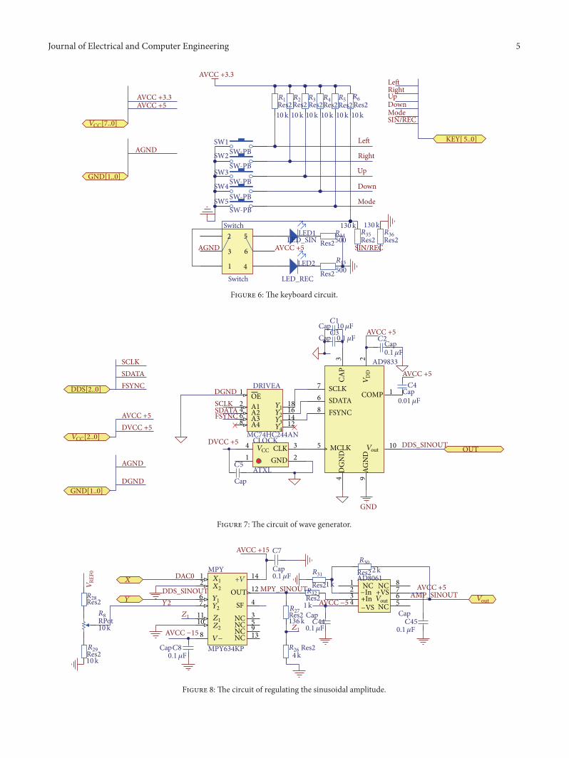
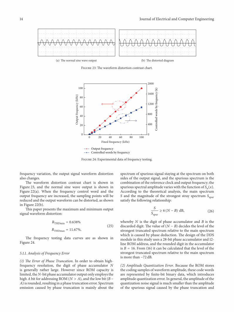
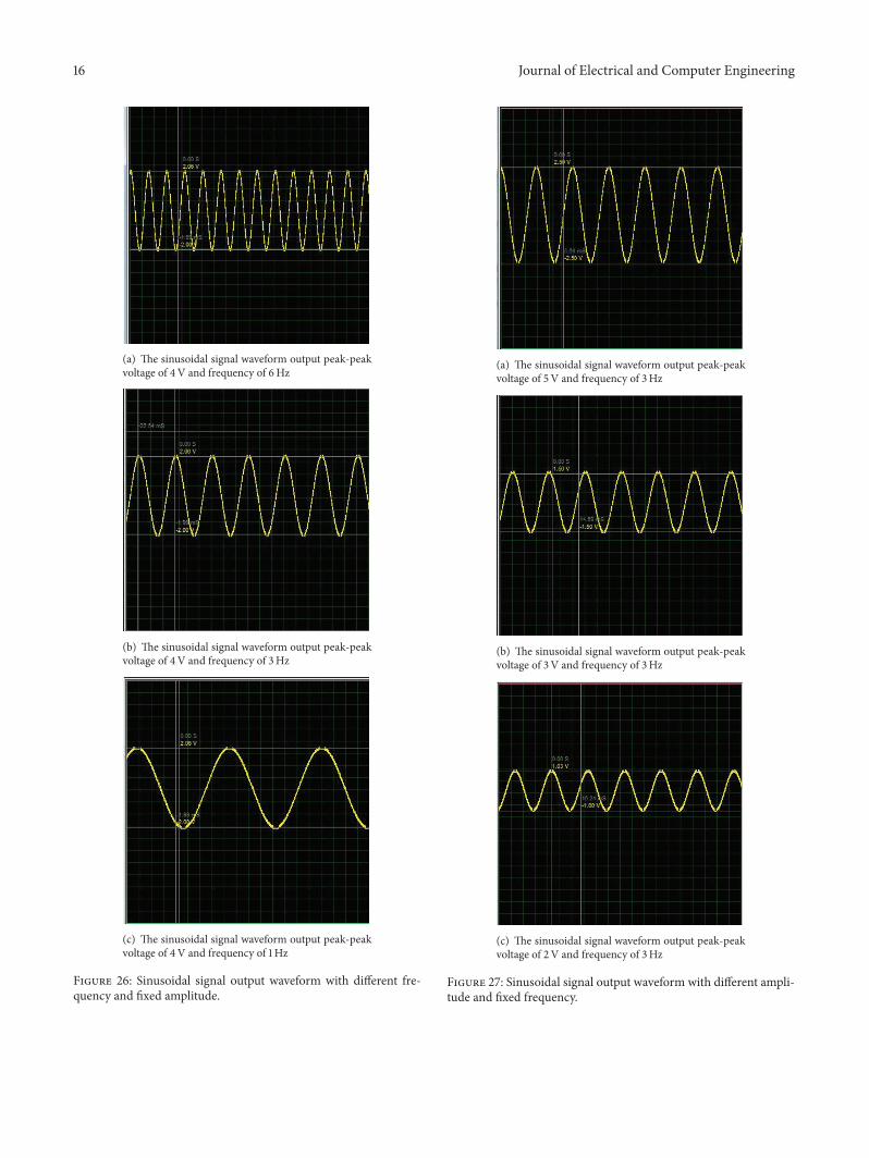

International Journal of
AerospaceEngineeringHindawi Publishing Corporationhttpwwwhindawicom Volume 2014
RoboticsJournal of
Hindawi Publishing Corporationhttpwwwhindawicom Volume 2014
Hindawi Publishing Corporationhttpwwwhindawicom Volume 2014
Active and Passive Electronic Components
Control Scienceand Engineering
Journal of
Hindawi Publishing Corporationhttpwwwhindawicom Volume 2014
International Journal of
RotatingMachinery
Hindawi Publishing Corporationhttpwwwhindawicom Volume 2014
Hindawi Publishing Corporation httpwwwhindawicom
Journal ofEngineeringVolume 2014
Submit your manuscripts athttpwwwhindawicom
VLSI Design
Hindawi Publishing Corporationhttpwwwhindawicom Volume 2014
Hindawi Publishing Corporationhttpwwwhindawicom Volume 2014
Shock and Vibration
Hindawi Publishing Corporationhttpwwwhindawicom Volume 2014
Civil EngineeringAdvances in
Acoustics and VibrationAdvances in
Hindawi Publishing Corporationhttpwwwhindawicom Volume 2014
Hindawi Publishing Corporationhttpwwwhindawicom Volume 2014
Electrical and Computer Engineering
Journal of
Advances inOptoElectronics
Hindawi Publishing Corporation httpwwwhindawicom
Volume 2014
The Scientific World JournalHindawi Publishing Corporation httpwwwhindawicom Volume 2014
SensorsJournal of
Hindawi Publishing Corporationhttpwwwhindawicom Volume 2014
Modelling amp Simulation in EngineeringHindawi Publishing Corporation httpwwwhindawicom Volume 2014
Hindawi Publishing Corporationhttpwwwhindawicom Volume 2014
Chemical EngineeringInternational Journal of Antennas and
Propagation
International Journal of
Hindawi Publishing Corporationhttpwwwhindawicom Volume 2014
Hindawi Publishing Corporationhttpwwwhindawicom Volume 2014
Navigation and Observation
International Journal of
Hindawi Publishing Corporationhttpwwwhindawicom Volume 2014
DistributedSensor Networks
International Journal of