Embed Size (px)
Citation preview
Hindawi Publishing CorporationJournal of NanomaterialsVolume 2011, Article ID 906237, 6 pagesdoi:10.1155/2011/906237
Research Article
Design and Analysis of a New Carbon Nanotube Full Adder Cell
M. H. Ghadiry,1 Asrulnizam Abd Manaf,1 M. T. Ahmadi,2 Hatef Sadeghi,2
and M. Nadi Senejani3
1 School of Electrical and Electronic Engineering, Universiti Sains Malaysia, Engineering Campus, 11800 Penang, Malaysia2 Faculty of Electrical Engineering, Universiti Teknologi Malaysia, 81310 Skudai, Malaysia3 Department of Computer Engineering, Islamic Azad University, Ashtian Branch, 39618-13347 Ashtian, Iran
Correspondence should be addressed to M. H. Ghadiry, [email protected]
Received 10 January 2011; Accepted 27 February 2011
Academic Editor: Theodorian Borca-Tasciuc
Copyright © 2011 M. H. Ghadiry et al. This is an open access article distributed under the Creative Commons Attribution License,which permits unrestricted use, distribution, and reproduction in any medium, provided the original work is properly cited.
A novel full adder circuit is presented. The main aim is to reduce power delay product (PDP) in the presented full adder cell.A new method is used in order to design a full-swing full adder cell with low number of transistors. The proposed full adderis implemented in MOSFET-like carbon nanotube technology and the layout is provided based on standard 32 nm technologyfrom MOSIS. The simulation results using HSPICE show that there are substantial improvements in both power and performanceof the proposed circuit compared to the latest designs. In addition, the proposed circuit has been implemented in conventional32 nm process to compare the benefits of using MOSFET-like carbon nanotubes in arithmetic circuits over conventional CMOStechnology. The proposed circuit can be applied in very high performance and ultra-low-power applications.
1. Introduction
Fundamental limitations of CMOS technology and antic-ipations of Moore’s law have motivated researchers tofind suitable alternative for these devices. Among severalproposed alternatives [1–5], carbon nanotube field effecttransistors seem to be a promising successor for CMOSdevices due to their superior characteristics [1, 6]. CNFETsindicate great potential further than silicon nanoelectronic,and significantly illustrate greater performance than conven-tional CMOS models specially in case of switching energy.Large transconductance of CNFETs creates huge interest innanoelectronic circuits’ application as well. As a result, manyworks have been done to model their properties [5–12].Several HSPICE models for CNFETs have been presented sofar such as [6, 8]. Among several SPICE models for CNFET,only in [6] practical device, nonidealises, and more than onetubes are modelled.
CNFETs’ high performance and low power consumptionproperties make them interesting to be used in the designof low-power-demanding arithmetic circuits. One of themost important blocks of these circuits is full adder cell[13–20], which are duplicated many times in buildingup larger circuits. In this paper, CNFET technology has
been employed, to make a very high-performance andultra-low-power adder from the proposed design. Onlythree CNTFET-based full adder cells have been presented sofar [19, 21–23]. However, parasitic capacitances and layouteffects have not been considered in them. In addition, all ofthose designs are based on adjusting threshold voltage (Vt)by manipulating diameter of tubes, which demands complexand expensive fabrication process [24, 25]. As a result, inaddition to attempting to achieve the least PDP among themost state-of-the-art designs in the literature, these twoissues have been addressed in this work by using the samediameter and threshold voltage for all devices and drawingpostlayout for every design based on a tailored industrialfabrication process [26, 27]. Moreover, the design is immuneagainst misaligned tubes fabrication defect [27].
2. Transistor Level Design Methodology
In practice, full adders are idle most of the time. In addition,in deep submicron technologies, static power is not asnegligible as it was in technologies higher than 0.18 μm. Oneway to reduce static power consumption and delay is full-swing design. However, it usually requires a high number
2 Journal of Nanomaterials
Table 1: Truth table of the cout module as a multiplexer.
Switch control In1 In2 Out
h = 0 a = 1 cout = 1
h = 1 c = 1 cout = 1
h = 1 c = 0 cout = 0
h = 0 a = 0 cout = 0
of transistors, which in turn increases power consumption.Therefore to achieve full-swing outputs with minimumtransistor count, the highest performance, and the loweststatic power consumption, a new method has been appliedto all three, sum, cout, and XOR-XNOR modules. In orderto show how the method works, design of cout moduleis verified here, which is the same approach that has beenapplied to sum and xor-xnor modules as well.
As (1) shows, both cout and sum can be expressedbased on h and h. Therefore, we used h and h as commonintermediate signals to implement sum and cout modulesusing the proposed method:
sum = a⊕ b ⊕ c,
sum =(a⊕ b
)(a⊕ b
)· c + (a⊕ b) · c,
sum = h · c + h · c,cout = ab + a c + bc,
cout =(a⊕ b
)· a + (a⊕ b) · c,
cout = h · a + h · c.
(1)
This method relies on design of multiplexers using passtransistors. Table 1 shows the truth table of the cout moduleas a multiplexer with h as its switch control, a and c as itsinputs, and cout as its output.
As Table 1 shows, each input has two states, and thus fouroutputs are possible, two of which are logic 1 and two logic0. Two rules must be followed in order to have full-swingoutputs.
(1) To design for logic 1 outputs, P-doped tubes must beused in series and all triggering signals, switch controland inputs, must be logic 0.
(2) To design for logic 0 outputs, N-doped tubes mustbe used in series and all triggering signals must belogic 1.
Therefore, in the first two rows of Table 1 there must beno logic 1 as input and in the last two rows no logic 0. As aresult, Table 2 is obtained by inverting inconsistent signals.
The result is shown in Table 3, which determines theselected signals and consequent logic to design cout module.
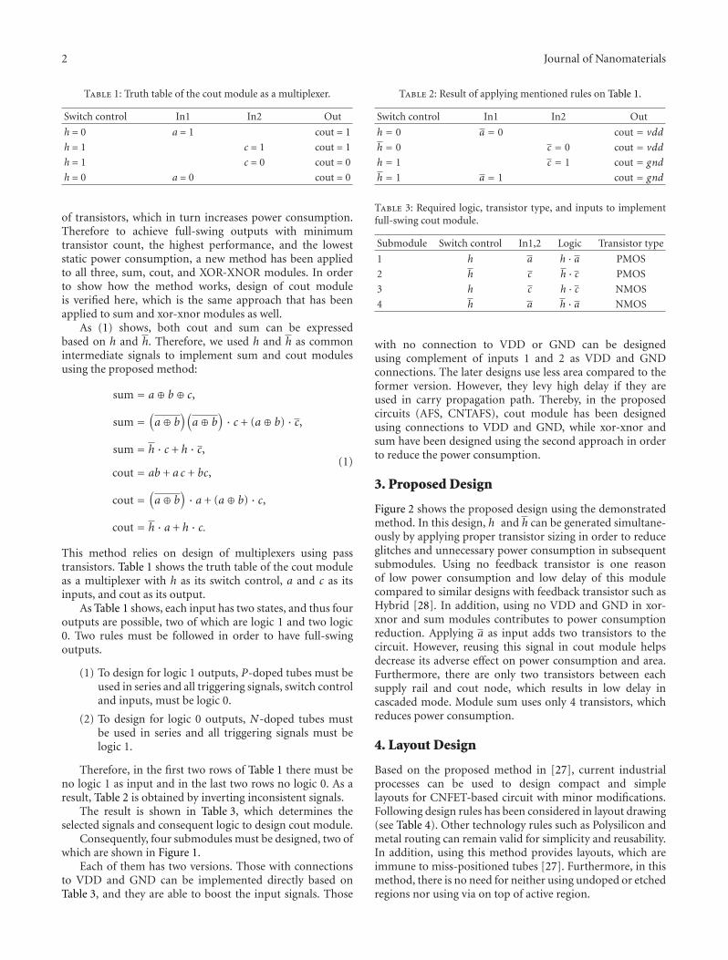
Consequently, four submodules must be designed, two ofwhich are shown in Figure 1.
Each of them has two versions. Those with connectionsto VDD and GND can be implemented directly based onTable 3, and they are able to boost the input signals. Those
Table 2: Result of applying mentioned rules on Table 1.
Switch control In1 In2 Out
h = 0 a = 0 cout = vdd
h = 0 c = 0 cout = vdd
h = 1 c = 1 cout = gnd
h = 1 a = 1 cout = gnd
Table 3: Required logic, transistor type, and inputs to implementfull-swing cout module.
Submodule Switch control In1,2 Logic Transistor type
1 h a h · a PMOS
2 h c h · c PMOS
3 h c h · c NMOS
4 h a h · a NMOS
with no connection to VDD or GND can be designedusing complement of inputs 1 and 2 as VDD and GNDconnections. The later designs use less area compared to theformer version. However, they levy high delay if they areused in carry propagation path. Thereby, in the proposedcircuits (AFS, CNTAFS), cout module has been designedusing connections to VDD and GND, while xor-xnor andsum have been designed using the second approach in orderto reduce the power consumption.
3. Proposed Design
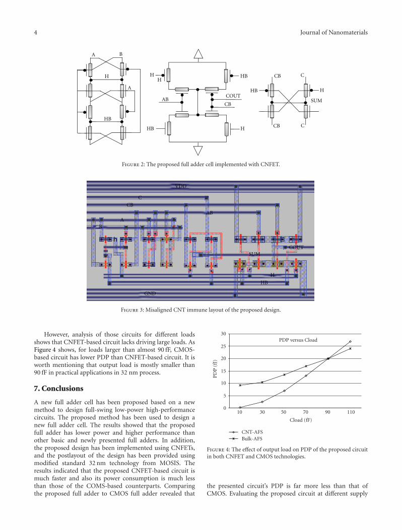
Figure 2 shows the proposed design using the demonstratedmethod. In this design, h and h can be generated simultane-ously by applying proper transistor sizing in order to reduceglitches and unnecessary power consumption in subsequentsubmodules. Using no feedback transistor is one reasonof low power consumption and low delay of this modulecompared to similar designs with feedback transistor such asHybrid [28]. In addition, using no VDD and GND in xor-xnor and sum modules contributes to power consumptionreduction. Applying a as input adds two transistors to thecircuit. However, reusing this signal in cout module helpsdecrease its adverse effect on power consumption and area.Furthermore, there are only two transistors between eachsupply rail and cout node, which results in low delay incascaded mode. Module sum uses only 4 transistors, whichreduces power consumption.
4. Layout Design
Based on the proposed method in [27], current industrialprocesses can be used to design compact and simplelayouts for CNFET-based circuit with minor modifications.Following design rules has been considered in layout drawing(see Table 4). Other technology rules such as Polysilicon andmetal routing can remain valid for simplicity and reusability.In addition, using this method provides layouts, which areimmune to miss-positioned tubes [27]. Furthermore, in thismethod, there is no need for neither using undoped or etchedregions nor using via on top of active region.

Journal of Nanomaterials 3
AB
COUT
CB
H HB
A
COUT
H HB
C
Sub -module 4 Sub -module 3
Figure 1: Submodules 3 and 4 of the module cout using theproposed method.
Table 4: Sample design rules used to design layout for CNFET-based circuit.
Design rule Description Value
Ls/Ld Length of source/drain 3λ
Lgs/Lgd Distance between gate and source/drain 2λ
Lg Length of gate 2λ
As shown in Figure 3 tailored 32 nm MOSIS processhas been employed on layout design of the CNFET-basedcircuit. Standard 32 nm process has been used to designlayouts of CMOS-based circuits. Parasitic capacitances forboth CNFET-based and CMOS-based circuits have beenextracted and included in simulations.
5. Simulation Environment
In order to show advantages of the proposed circuit overexisted adders in the literature, the proposed circuits havebeen compared with several circuits from the literature.CMOS [14] as basic circuit for comparison in standardCMOS technology and Hybrid [28] as one of the best circuitsin terms of power and performance are also implemented instandard CMOS. There are only five CNTFET-based addersin the literature, all of which have been compared with ourdesign. Design 1 [21], design 1 in [22], which is the sameas design 2 in [21], the proposed adder in [22], and thepresented full adder in [19] are called CNTD1, CNTD2,CNTD3, and CNTD4 in this paper.
Eight cells of each mentioned full adder have beencascaded to make an 8-bit ripple carry adder. All inputs comefrom input buffers, which are two cascaded inverters in thesame technology. The W/L (width/length) ratios for invertersare made to be equal to 5/3 and 12/5. In CNFET devices,these values are 4 and 8 tubes per device, respectively. Otherparameters of CNFET devices are the same as the defaultvalues for semiconducting tube [6]. Transistor sizing hasbeen done to achieve the best PDP in each circuit. In case
of CNFET device, the number of tubes has been changed inorder to gain the best PDP. To generate input patterns andconsider the worst cases in all designs, the same method as[29] has been used in this work to identify the critical path ofeach design to spot the longest delay.
The performance and PDP of the under test circuitshave been evaluated based on worst-case propagation delay.Propagation delay is calculated from 50% of input voltagelevel to 50% of output voltage level. Rise time and fall timeof input signals in all simulations are 5% of the input signal’spulse width. As adder circuits are idle most of the time wecalculated P20% based on formula P20% = 0.2Pactive×0.8PIdle,where the active power is the power consumption of thecircuit when inputs are triggered at 300 MHz frequency andidle power is the average static power of the circuit forseveral combinations of inputs. Area has been calculatedby multiplication of total height and width of the circuits’postlayout. CNFET model presented in [6] has been appliedin this research, and simulations have been carried out usingHSPICE.
6. Results and Discussion
Table 5 shows the result of simulation for 8-bit ripplecarry adder (RCA) including parasitic capacitances andnonidealises of both Carbon nanotube and CMOS devices.Symbol Φ in Table 5 shows that product of PDP andarea. Apparently, the proposed circuit in CNFET technology(CNAFS) outperforms the other circuits in terms of PDP.This is due to full-swing design of the xor-xnor module withlow number of transistors, which reduces leakage current inboth itself and subsequent modules and improves the delaycompared to other circuits. In addition, boosting power ofcout module contributes to more delay reduction. Modulesum has low driving ability but low power consumption. Asit plays no role in critical path, low power consumption ismore important than high driving capability on its design.
Comparing the proposed CNFET-based with CMOS-based (AFS) circuits reveals that PDP has been improved atleast 8 times. In terms of area, although drawing layout usingthe method proposed in [27] has some limitations, the areais still less than that of AFS. CNAFS with 1 GHz maximumoperating frequency and 1.17 μw power consumption is thefastest circuit and lowest power-consuming circuit among allsimulated circuits. Other CN-based designs, CNTD1–4, havehigher PDP than our design mostly because of large inputcapacitances imposing high delay. In order to gain the leastPDP transistor sizes must be scaled up, which cause higherpower consumption. CNTD1 shows high static power due touse of ratio logic in its design. Using 4 inverters in CNTD4contributes to high power consumption. However, its delayis slightly less than CNAFS due to boosting power of theseinverters.
Table 6 shows power and performance of the proposedcircuit at 0.6 and 0.9 V supply voltage. By decreasing VDDfrom 0.9 V to 0.6 V, PDP of CNAFS increased from 1.17to 1.57, while it increased from 9.88 to 17.58 for AFS. Inother words, CNFET-based design is less sensitive to voltagevariation than CMOS-based one.
4 Journal of Nanomaterials
A B
H
A
HB
HH
HB
ABCOUT
CB
HHB
HB
CB C
CB C
H
SUM
Figure 2: The proposed full adder cell implemented with CNFET.
VDD
C
CB
AB
GND
A
SUMCOUT
H
HB
B
Figure 3: Misaligned CNT immune layout of the proposed design.
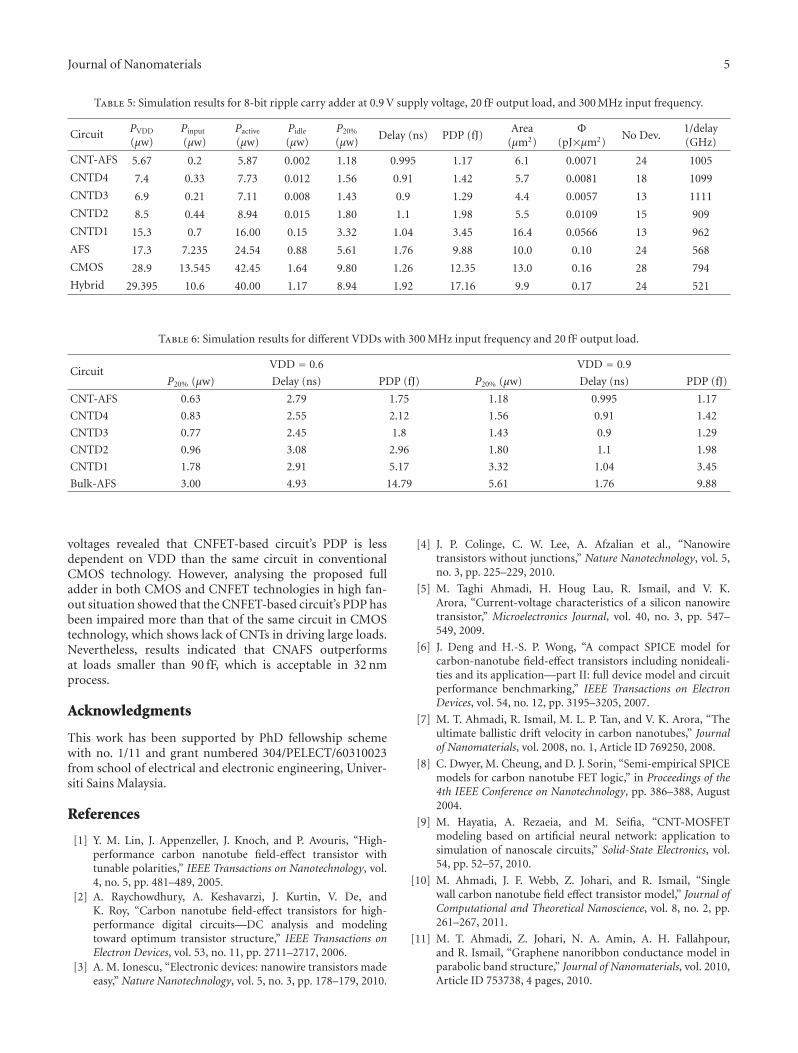
However, analysis of those circuits for different loadsshows that CNFET-based circuit lacks driving large loads. AsFigure 4 shows, for loads larger than almost 90 fF, CMOS-based circuit has lower PDP than CNFET-based circuit. It isworth mentioning that output load is mostly smaller than90 fF in practical applications in 32 nm process.
7. Conclusions
A new full adder cell has been proposed based on a newmethod to design full-swing low-power high-performancecircuits. The proposed method has been used to design anew full adder cell. The results showed that the proposedfull adder has lower power and higher performance thanother basic and newly presented full adders. In addition,the proposed design has been implemented using CNFETs,and the postlayout of the design has been provided usingmodified standard 32 nm technology from MOSIS. Theresults indicated that the proposed CNFET-based circuit ismuch faster and also its power consumption is much lessthan those of the COMS-based counterparts. Comparingthe proposed full adder to CMOS full adder revealed that
0
5
PD
P(f
J)
10
15
20
25
30
10
CNT-AFSBulk-AFS
30 50 70 90 110
Cload (fF)
PDP versus Cload
Figure 4: The effect of output load on PDP of the proposed circuitin both CNFET and CMOS technologies.
the presented circuit’s PDP is far more less than that ofCMOS. Evaluating the proposed circuit at different supply
Journal of Nanomaterials 5
Table 5: Simulation results for 8-bit ripple carry adder at 0.9 V supply voltage, 20 fF output load, and 300 MHz input frequency.
Circuit PVDD
(μw)Pinput
(μw)Pactive
(μw)Pidle
(μw)P20%
(μw)Delay (ns) PDP (fJ)
Area(μm2)
Φ(pJ×μm2)
No Dev.1/delay(GHz)
CNT-AFS 5.67 0.2 5.87 0.002 1.18 0.995 1.17 6.1 0.0071 24 1005
CNTD4 7.4 0.33 7.73 0.012 1.56 0.91 1.42 5.7 0.0081 18 1099
CNTD3 6.9 0.21 7.11 0.008 1.43 0.9 1.29 4.4 0.0057 13 1111
CNTD2 8.5 0.44 8.94 0.015 1.80 1.1 1.98 5.5 0.0109 15 909
CNTD1 15.3 0.7 16.00 0.15 3.32 1.04 3.45 16.4 0.0566 13 962
AFS 17.3 7.235 24.54 0.88 5.61 1.76 9.88 10.0 0.10 24 568
CMOS 28.9 13.545 42.45 1.64 9.80 1.26 12.35 13.0 0.16 28 794
Hybrid 29.395 10.6 40.00 1.17 8.94 1.92 17.16 9.9 0.17 24 521
Table 6: Simulation results for different VDDs with 300 MHz input frequency and 20 fF output load.
CircuitVDD = 0.6 VDD = 0.9
P20% (μw) Delay (ns) PDP (fJ) P20% (μw) Delay (ns) PDP (fJ)
CNT-AFS 0.63 2.79 1.75 1.18 0.995 1.17
CNTD4 0.83 2.55 2.12 1.56 0.91 1.42
CNTD3 0.77 2.45 1.8 1.43 0.9 1.29
CNTD2 0.96 3.08 2.96 1.80 1.1 1.98
CNTD1 1.78 2.91 5.17 3.32 1.04 3.45
Bulk-AFS 3.00 4.93 14.79 5.61 1.76 9.88
voltages revealed that CNFET-based circuit’s PDP is lessdependent on VDD than the same circuit in conventionalCMOS technology. However, analysing the proposed fulladder in both CMOS and CNFET technologies in high fan-out situation showed that the CNFET-based circuit’s PDP hasbeen impaired more than that of the same circuit in CMOStechnology, which shows lack of CNTs in driving large loads.Nevertheless, results indicated that CNAFS outperformsat loads smaller than 90 fF, which is acceptable in 32 nmprocess.
Acknowledgments
This work has been supported by PhD fellowship schemewith no. 1/11 and grant numbered 304/PELECT/60310023from school of electrical and electronic engineering, Univer-siti Sains Malaysia.
References
[1] Y. M. Lin, J. Appenzeller, J. Knoch, and P. Avouris, “High-performance carbon nanotube field-effect transistor withtunable polarities,” IEEE Transactions on Nanotechnology, vol.4, no. 5, pp. 481–489, 2005.
[2] A. Raychowdhury, A. Keshavarzi, J. Kurtin, V. De, andK. Roy, “Carbon nanotube field-effect transistors for high-performance digital circuits—DC analysis and modelingtoward optimum transistor structure,” IEEE Transactions onElectron Devices, vol. 53, no. 11, pp. 2711–2717, 2006.
[3] A. M. Ionescu, “Electronic devices: nanowire transistors madeeasy,” Nature Nanotechnology, vol. 5, no. 3, pp. 178–179, 2010.
[4] J. P. Colinge, C. W. Lee, A. Afzalian et al., “Nanowiretransistors without junctions,” Nature Nanotechnology, vol. 5,no. 3, pp. 225–229, 2010.
[5] M. Taghi Ahmadi, H. Houg Lau, R. Ismail, and V. K.Arora, “Current-voltage characteristics of a silicon nanowiretransistor,” Microelectronics Journal, vol. 40, no. 3, pp. 547–549, 2009.
[6] J. Deng and H.-S. P. Wong, “A compact SPICE model forcarbon-nanotube field-effect transistors including nonideali-ties and its application—part II: full device model and circuitperformance benchmarking,” IEEE Transactions on ElectronDevices, vol. 54, no. 12, pp. 3195–3205, 2007.
[7] M. T. Ahmadi, R. Ismail, M. L. P. Tan, and V. K. Arora, “Theultimate ballistic drift velocity in carbon nanotubes,” Journalof Nanomaterials, vol. 2008, no. 1, Article ID 769250, 2008.
[8] C. Dwyer, M. Cheung, and D. J. Sorin, “Semi-empirical SPICEmodels for carbon nanotube FET logic,” in Proceedings of the4th IEEE Conference on Nanotechnology, pp. 386–388, August2004.
[9] M. Hayatia, A. Rezaeia, and M. Seifia, “CNT-MOSFETmodeling based on artificial neural network: application tosimulation of nanoscale circuits,” Solid-State Electronics, vol.54, pp. 52–57, 2010.
[10] M. Ahmadi, J. F. Webb, Z. Johari, and R. Ismail, “Singlewall carbon nanotube field effect transistor model,” Journal ofComputational and Theoretical Nanoscience, vol. 8, no. 2, pp.261–267, 2011.
[11] M. T. Ahmadi, Z. Johari, N. A. Amin, A. H. Fallahpour,and R. Ismail, “Graphene nanoribbon conductance model inparabolic band structure,” Journal of Nanomaterials, vol. 2010,Article ID 753738, 4 pages, 2010.
6 Journal of Nanomaterials
[12] M. T. Ahmadi, M. L. P. Tan, R. Ismail, and V. K. Arora,“The high-field drift velocity in degenerately-doped siliconnanowires,” International Journal of Nanotechnology, vol. 6, no.7-8, pp. 601–617, 2009.
[13] M. H. Ghadiry, H. Mohammadi, and M. N. Senejani, “Twonew low power high performance full adder with minimumgates,” International Journal of Electrical and InformationEngineering, vol. 3, pp. 124–131, 2009.
[14] K. Navi, M. Maeen, V. Foroutan, S. Timarchi, and O.Kavehei, “A novel low-power full-adder cell for low voltage,”Integration, the VLSI Journal, vol. 42, no. 4, pp. 457–467, 2009.
[15] V. Foroutan, K. Navi, and M. Haghparast, “A new low powerdynamic full adder cell based on majority function,” WorldApplied Sciences Journal, vol. 4, pp. 133–141, 2008.
[16] M. Nadi, M. H. Ghadiry, and M. K. Dermany, “The effect ofnumber of virtual channel on NOC EDP,” Journal of AppliedMathematics & Informatics, vol. 2010, pp. 539–551, 2010.
[17] M. H. Ghadiry, A. Khari, and M. N. Senejani, “A new full-swing full adder based on new logic approach,” World AppliedSciences Journal, vol. 1, 2011.
[18] M. H. Ghadiry, A. K. A’Ain, and M. N. Senejani, “Design andanalysis of a novel low PDP full adder cell,” Journal of Circuits,Systems, and Computers, vol. 20, 2011.
[19] K. Navi, M. Rashtian, A. Khatir, P. Keshavarzian, and O.Hashemipour, “High speed capacitor-inverter based carbonnanotube full adder,” Nanoscale Research Letters, vol. 5, no. 5,pp. 859–862, 2010.
[20] M. N. Senejani, M. Hosseinghadiry, and M. Miryahyaei, “Lowdynamic power high performance adder,” in Proceedings ofInternational Conference on Future Computer and Communi-cation (ICFCC ’09), pp. 482–486, April 2009.
[21] K. Navi, A. Momeni, F. Sharifi, and P. Keshavarzian, “Twonovel ultra high speed carbon nanotube Full-Adder cells,”IEICE Electronics Express, vol. 6, no. 19, pp. 1395–1401, 2009.
[22] K. Navi, R. S. Rad, M. H. Moaiyeri, and A. Momeni, “A low-loltage and energy-efficient full adder cell based on carbonnanotube technology,” Nano-Micro Letters, vol. 2, pp. 114–120, 2010.
[23] K. Navi, M. Maeen, V. Foroutan, S. Timarchi, and O.Kavehei, “A novel low-power full-adder cell for low voltage,”Integration, the VLSI Journal, vol. 42, no. 4, pp. 457–467, 2009.
[24] C. V. Nguyen, Q. Ye, and M. Meyyappan, “Carbon nanotubetips for scanning probe microscopy: fabrication and highaspect ratio nanometrology,” Measurement Science and Tech-nology, vol. 16, no. 11, pp. 2138–2146, 2005.
[25] C. Wang, J. Zhang, K. Ryu, A. Badmaev, L. G. de Arco, and C.Zhou, “Wafer-scale fabrication of separated carbon nanotubethin-film transistors for display applications,” Nano Letters,vol. 9, no. 12, pp. 4285–4291, 2009.
[26] 2011, http://www.mosis.com/ibm/ibm processes.html.[27] S. Bobba, J. Zhang, A. Pullini, D. Atienza, and G. De Micheli,
“Design of compact imperfection-immune CNFET layouts forstandard-cell-based logic synthesis,” in Proceedings of Design,Automation and Test in Europe Conference and Exhibition(DATE ’09), pp. 616–621, April 2009.
[28] S. Goel, A. Kumar, and M. A. Bayoumi, “Design of robust,energy-efficient full adders for deep-submicrometer designusing hybrid-CMOS logic style,” IEEE Transactions on VeryLarge Scale Integration (VLSI) Systems, vol. 14, no. 12, pp.1309–1321, 2006.
[29] J. F. Lin, Y. T. Hwang, M. H. Sheu, and C. C. Ho, “A novel high-speed and energy efficient 10-transistor full adder design,”IEEE Transactions on Circuits and Systems I: Regular Papers,vol. 54, no. 5, pp. 1050–1059, 2007.

Submit your manuscripts athttp://www.hindawi.com
ScientificaHindawi Publishing Corporationhttp://www.hindawi.com Volume 2014
CorrosionInternational Journal of
Hindawi Publishing Corporationhttp://www.hindawi.com Volume 2014
Polymer ScienceInternational Journal of
Hindawi Publishing Corporationhttp://www.hindawi.com Volume 2014
Hindawi Publishing Corporationhttp://www.hindawi.com Volume 2014
CeramicsJournal of
Hindawi Publishing Corporationhttp://www.hindawi.com Volume 2014
CompositesJournal of
NanoparticlesJournal of
Hindawi Publishing Corporationhttp://www.hindawi.com Volume 2014
Hindawi Publishing Corporationhttp://www.hindawi.com Volume 2014
International Journal of
Biomaterials
Hindawi Publishing Corporationhttp://www.hindawi.com Volume 2014
NanoscienceJournal of
TextilesHindawi Publishing Corporation http://www.hindawi.com Volume 2014
Journal of
NanotechnologyHindawi Publishing Corporationhttp://www.hindawi.com Volume 2014
Journal of
CrystallographyJournal of
Hindawi Publishing Corporationhttp://www.hindawi.com Volume 2014
The Scientific World JournalHindawi Publishing Corporation http://www.hindawi.com Volume 2014
Hindawi Publishing Corporationhttp://www.hindawi.com Volume 2014
CoatingsJournal of
Advances in
Materials Science and EngineeringHindawi Publishing Corporationhttp://www.hindawi.com Volume 2014
Smart Materials Research
Hindawi Publishing Corporationhttp://www.hindawi.com Volume 2014
Hindawi Publishing Corporationhttp://www.hindawi.com Volume 2014
MetallurgyJournal of
Hindawi Publishing Corporationhttp://www.hindawi.com Volume 2014
BioMed Research International
MaterialsJournal of
Hindawi Publishing Corporationhttp://www.hindawi.com Volume 2014
Nano
materials
Hindawi Publishing Corporationhttp://www.hindawi.com Volume 2014
Journal ofNanomaterials