Embed Size (px)
Citation preview

of sequence introgression between N. vitripennisandN. longicornis (18). These results indicate thatregulatory evolution of upd-like probably occurredin two separateNasonia lineages, either by parallelreductions in N. vitripennis and N. longicornis orby reduction in an ancestral Nasonia lineage fol-lowed by expansion in theN. giraulti lineage. Thisobservation plus the role of three subregions thatwe have identified between N. vitripennis andN. giraulti suggests that unpaired-like is a hotspotfor wing size evolution in Nasonia.
Discussion. This study determined the geneticbasis of wdw, a major component of the male-specific wing size difference betweenN. vitripennisand N. giraulti. Our data indicate that upd-likecauses the spatial changes in cell proliferationand growth within the wing and that upd-like is ahotspot for size and shape evolution in Nasonia.Unpaired (upd) inD.melanogaster is a ligand forthe JAK/STAT pathway (21). This pathway’s rolein cell proliferation makes it a plausible target ofmorphological evolution, though it is not yet knownwhether upd-like mediates its effects in Nasoniathrough JAK/STAT or other pathways. Nasoniaupd-like appears to be particularly susceptible towing growth–altering changes, which indicatesthat the gene might have a specialized role in spec-ifying organ size in the growth gene network.Considering that many size and shape differencesbetween animals are due to differences in cell num-bers (9), upd-like genes could be hotspots of sizeand shape evolution in other species as well.
Using a phenotype-based positional cloningapproach, we have identified two different majorQTL genes (wdw andws1) that are responsible forsex-specific differences in wing development be-tween closely related Nasonia species. From what
is known about fly wing development (22–24),the alternative candidate gene approach wouldnot have predicted the role of either upd or dsx inNasonia wing size. Nevertheless, both genes ap-pear to be homologs of functionally conserveddevelopmental regulatory genes, which is consist-ent with the hypothesis that core developmentalgenes tend to be involved in morphological evo-lution (25, 26). It has also been argued that non-coding cis-regulatory changes could play a centralrole in developmental differences between species(27, 28). Our findings support this view and fur-ther implicate growth-regulating genes in organ-specific size and shape evolution.
References and Notes1. G. Galilei, Dialogues Concerning Two New Sciences,
H. Crew, A. De Salvio, Transls. (MacMillan, New York, 1914).2. C. Darwin, On the Origin of Species by Means of Natural
Selection, or the Preservation of Favored Races in theStruggle for Life (John Murray, London, 1859).
3. J. B. Losos, T. R. Jackman, A. Larson, K. Queiroz,L. Rodriguez-Schettino, Science 279, 2115 (1998).
4. A. Abzhanov, M. Protas, B. R. Grant, P. R. Grant,C. J. Tabin, Science 305, 1462 (2004).
5. S. W. McKechnie et al., Mol. Ecol. 19, 775 (2010).6. M. D. Shapiro et al., Nature 428, 717 (2004).7. D. L. Stern, V. Orgogozo, Evolution 62, 2155 (2008).8. D. W. Loehlin et al., PLoS Genet. 6, e1000821 (2010).9. B. A. Edgar, Nat. Rev. Genet. 7, 907 (2006).10. T. Lecuit, L. Le Goff, Nature 450, 189 (2007).11. D. W. Loehlin, L. S. Enders, J. H. Werren, Heredity 104,
260 (2010).12. R. Raychoudhury et al., Heredity 104, 278 (2010).13. J. H. Werren, D. W. Loehlin, in Emerging Model
Organisms, vol. 2, D. A. Crotty, A. Gann, Eds.(Cold Spring Harbor Laboratory Press, Cold SpringHarbor, NY, 2009), pp. 267–298.
14. R. F. Weston, I. Qureshi, J. H. Werren, J. Evol. Biol. 12,586 (1999).
15. C. S. Raymond, M. W. Murphy, M. G. O’Sullivan,V. J. Bardwell, D. Zarkower, Genes Dev. 14, 2587 (2000).
16. L. E. Sanders, M. N. Arbeitman, Dev. Biol. 320, 378 (2008).17. Materials and methods are available as supporting
material on Science Online.18. Supporting text is available as supporting material on
Science Online.19. J. S. Rawlings, K. M. Rosler, D. A. Harrison, J. Cell Sci.
117, 1281 (2004).20. J. H. Werren et al., Science 327, 343 (2010).21. N. I. Arbouzova, M. P. Zeidler, Development 133, 2605
(2006).22. J. C. Hombría, S. Brown, S. Häder, M. P. Zeidler, Dev.
Biol. 288, 420 (2005).23. T. Mukherjee, J. C. Hombría, M. P. Zeidler, Oncogene 24,
2503 (2005).24. C. C. Robinett, A. G. Vaughan, J. M. Knapp, B. S. Baker,
PLoS Biol. 8, e1000365 (2010).25. T. Werner, S. Koshikawa, T. M. Williams, S. B. Carroll,
Nature 464, 1143 (2010).26. B. R. Wasik, D. J. Rose, A. P. Moczek, Evol. Dev. 12, 353
(2010).27. D. L. Stern, Evolution 54, 1079 (2000).28. S. B. Carroll, PLoS Biol. 3, e245 (2005).29. R. Raychoudhury, L. Baldo, D. C. Oliveira, J. H. Werren,
Evolution 63, 165 (2009).
Acknowledgments: We thank L. Gu and J. Sysol for volunteerassistance with mapping; M. Rosenberg for sharing theNasonia wingless plasmid; and H. Jasper, J. D. Lambert,M. Welte, D. Stern, D. Presgraves, D. Wheeler, R. Edwards,A. Avery, and M. Clark for advice and technical assistance.This work was supported by NSF Doctoral DissertationImprovement Grant DEB-0910017 to D.W.L. and NIH grants5R01 GM070026-04 and 5R24 GM084917-04 to J.H.W.Sequences are deposited at GenBank with accessionsJQ082366 to JQ082369.
Supporting Online Materialwww.sciencemag.org/cgi/content/full/335/6071/943/DC1Materials and MethodsSOM TextFigs. S1 to S9Tables S1 to S3References (30–32)
12 October 2011; accepted 10 January 201210.1126/science.1215193
REPORTS
Field-Effect TunnelingTransistor Based on VerticalGraphene HeterostructuresL. Britnell,1 R. V. Gorbachev,2 R. Jalil,2 B. D. Belle,2 F. Schedin,2 A. Mishchenko,1
T. Georgiou,1 M. I. Katsnelson,3 L. Eaves,4 S. V. Morozov,5 N. M. R. Peres,6,7 J. Leist,8
A. K. Geim,1,2* K. S. Novoselov,1* L. A. Ponomarenko1*
An obstacle to the use of graphene as an alternative to silicon electronics has been the absenceof an energy gap between its conduction and valence bands, which makes it difficult to achieve lowpower dissipation in the OFF state. We report a bipolar field-effect transistor that exploits the lowdensity of states in graphene and its one-atomic-layer thickness. Our prototype devices are grapheneheterostructures with atomically thin boron nitride or molybdenum disulfide acting as a verticaltransport barrier. They exhibit room-temperature switching ratios of ≈50 and ≈10,000, respectively.Such devices have potential for high-frequency operation and large-scale integration.
The performance of graphene-based fieldeffect transistors (FETs) has been ham-pered by graphene’s metallic conductivity
at the neutrality point (NP) and the unimpededelectron transport through potential barrierscaused by Klein tunneling, which limit the achie-
vable ON-OFF switching ratios to ~103 and thoseachieved so far at room temperature to <10 (1–7).These low ratios are sufficient for individual high-frequency transistors and analog electronics (4–7),but they present a fundamental problem for anyrealistic prospect of graphene-based integrated cir-cuits (1–7). A possible solution is to open a bandgap in graphene—for example, by using bilayer
1School of Physics and Astronomy, University of Manchester,Manchester M13 9PL, UK. 2Manchester Centre for Meso-science and Nanotechnology, University of Manchester, Man-chester M13 9PL, UK. 3Institute for Molecules and Materials,Radboud University of Nijmegen, 6525 AJ Nijmegen, Nether-lands. 4School of Physics and Astronomy, University of Notting-ham, Nottingham NG7 2RD, UK. 5Institute for MicroelectronicsTechnology, 142432 Chernogolovka, Russia. 6Departamento deFísica, Universidade do Minho, P-4710-057, Braga, Portugal.7Graphene Research Centre and Department of Physics, NationalUniversity of Singapore, 2 Science Drive 3, 117542 Singapore.8Momentive Performance Materials, 22557 West Lunn Road,Strongsville, OH 44070, USA.
*To whom correspondence should be addressed. E-mail:[email protected] (A.K.G.); [email protected](K.S.N.); [email protected] (L.A.P.)
www.sciencemag.org SCIENCE VOL 335 24 FEBRUARY 2012 947
graphene (8, 9), nanoribbons (10, 11), quantumdots (11), or chemical derivatives (12)—but it hasproven difficult to achieve high ON-OFF ratioswithout degrading graphene’s electronic quality.
We report an alternative graphene transistorarchitecture—namely, a field-effect transistor basedon quantum tunneling (13–17) from a grapheneelectrode through a thin insulating barrier [in ourcase, hexagonal boron nitride (hBN) or molybde-num disulfide of ~1 nm thickness]. The operationof the device relies on the voltage tunability ofthe tunneling density of states (DOS) in grapheneand of the effective height D of the tunnel barrieradjacent to the graphene electrode. To illustrate theproposed concept, we concentrate on graphene-hBN-graphene devices [an alternative barrier ma-terial (MoS2) is discussed in (18)].
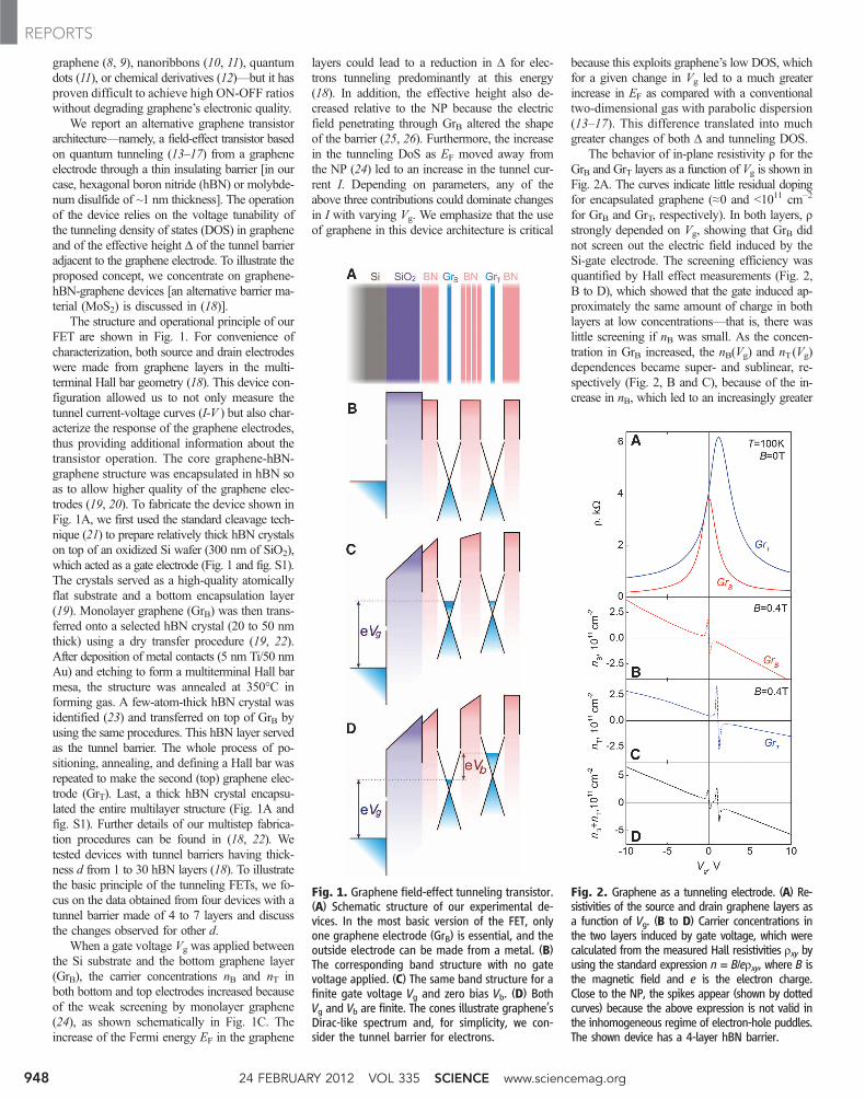
The structure and operational principle of ourFET are shown in Fig. 1. For convenience ofcharacterization, both source and drain electrodeswere made from graphene layers in the multi-terminal Hall bar geometry (18). This device con-figuration allowed us to not only measure thetunnel current-voltage curves (I-V ) but also char-acterize the response of the graphene electrodes,thus providing additional information about thetransistor operation. The core graphene-hBN-graphene structure was encapsulated in hBN soas to allow higher quality of the graphene elec-trodes (19, 20). To fabricate the device shown inFig. 1A, we first used the standard cleavage tech-nique (21) to prepare relatively thick hBN crystalson top of an oxidized Si wafer (300 nm of SiO2),which acted as a gate electrode (Fig. 1 and fig. S1).The crystals served as a high-quality atomicallyflat substrate and a bottom encapsulation layer(19). Monolayer graphene (GrB) was then trans-ferred onto a selected hBN crystal (20 to 50 nmthick) using a dry transfer procedure (19, 22).After deposition of metal contacts (5 nm Ti/50 nmAu) and etching to form a multiterminal Hall barmesa, the structure was annealed at 350°C informing gas. A few-atom-thick hBN crystal wasidentified (23) and transferred on top of GrB byusing the same procedures. This hBN layer servedas the tunnel barrier. The whole process of po-sitioning, annealing, and defining a Hall bar wasrepeated to make the second (top) graphene elec-trode (GrT). Last, a thick hBN crystal encapsu-lated the entire multilayer structure (Fig. 1A andfig. S1). Further details of our multistep fabrica-tion procedures can be found in (18, 22). Wetested devices with tunnel barriers having thick-ness d from 1 to 30 hBN layers (18). To illustratethe basic principle of the tunneling FETs, we fo-cus on the data obtained from four devices with atunnel barrier made of 4 to 7 layers and discussthe changes observed for other d.
When a gate voltage Vg was applied betweenthe Si substrate and the bottom graphene layer(GrB), the carrier concentrations nB and nT inboth bottom and top electrodes increased becauseof the weak screening by monolayer graphene(24), as shown schematically in Fig. 1C. Theincrease of the Fermi energy EF in the graphene
layers could lead to a reduction in D for elec-trons tunneling predominantly at this energy(18). In addition, the effective height also de-creased relative to the NP because the electricfield penetrating through GrB altered the shapeof the barrier (25, 26). Furthermore, the increasein the tunneling DoS as EF moved away fromthe NP (24) led to an increase in the tunnel cur-rent I. Depending on parameters, any of theabove three contributions could dominate changesin I with varying Vg. We emphasize that the useof graphene in this device architecture is critical
because this exploits graphene’s low DOS, whichfor a given change in Vg led to a much greaterincrease in EF as compared with a conventionaltwo-dimensional gas with parabolic dispersion(13–17). This difference translated into muchgreater changes of both D and tunneling DOS.
The behavior of in-plane resistivity r for theGrB and GrT layers as a function of Vg is shown inFig. 2A. The curves indicate little residual dopingfor encapsulated graphene (≈0 and <1011 cm−2
for GrB and GrT, respectively). In both layers, rstrongly depended on Vg, showing that GrB didnot screen out the electric field induced by theSi-gate electrode. The screening efficiency wasquantified by Hall effect measurements (Fig. 2,B to D), which showed that the gate induced ap-proximately the same amount of charge in bothlayers at low concentrations—that is, there waslittle screening if nB was small. As the concen-tration in GrB increased, the nB(Vg) and nT(Vg)dependences became super- and sublinear, re-spectively (Fig. 2, B and C), because of the in-crease in nB, which led to an increasingly greater
Fig. 1. Graphene field-effect tunneling transistor.(A) Schematic structure of our experimental de-vices. In the most basic version of the FET, onlyone graphene electrode (GrB) is essential, and theoutside electrode can be made from a metal. (B)The corresponding band structure with no gatevoltage applied. (C) The same band structure for afinite gate voltage Vg and zero bias Vb. (D) BothVg and Vb are finite. The cones illustrate graphene’sDirac-like spectrum and, for simplicity, we con-sider the tunnel barrier for electrons.
Fig. 2. Graphene as a tunneling electrode. (A) Re-sistivities of the source and drain graphene layers asa function of Vg. (B to D) Carrier concentrations inthe two layers induced by gate voltage, which werecalculated from the measured Hall resistivities rxy byusing the standard expression n = B/erxy, where B isthe magnetic field and e is the electron charge.Close to the NP, the spikes appear (shown by dottedcurves) because the above expression is not valid inthe inhomogeneous regime of electron-hole puddles.The shown device has a 4-layer hBN barrier.
24 FEBRUARY 2012 VOL 335 SCIENCE www.sciencemag.org948
REPORTS

fraction of the gate-induced electric field beingscreened out by GrB (18). Hence, more electronsaccumulated in the bottom graphene electrode,and fewer reached the top electrode. The totalcharge accumulated in both layers varied linear-ly in Vg (Fig. 2D), as expected. We could describethe observed redistribution of the charge be-tween the two graphene layers in terms of thecorresponding sequential circuit including thequantum capacitance (13, 27) of the graphenelayers (fig. S2). For a parabolic band, the ratiobetween nB and nt would be independent on Vg,and therefore, the electric field penetrating intothe tunnel barrier would be substantially reducedeven in the limit of zero nB (13).
A bias voltage Vb applied between GrB andGrT gave rise to a tunnel current through thethin hBN barrier that scaled with device area.I-V characteristics for one of our devices at var-ious Vg are shown in Fig. 3A. First, we considerthe case of zero Vg. At low Vb, I was linear inbias, yielding a tunnel resistivity rT = Vb/I ≈100gigohms mm2 for this hBN thickness. At highervoltages (Vb above ~0.1 V), I grew more rap-idly. The I-V curves could be described (Fig.3A, inset, and fig. S3) by the standard quantum-tunneling formulae (25, 26), assuming energyconservation but no momentum conservation atthe mismatched graphene-hBN interface (28).
As shown below, we could distinguish ex-perimentally between electron and hole tunnelingand found that the tunneling was due to holes.This result is in agreement with a recent theoryfor the graphene-hBN interface (29), which reportsa separation between the Dirac point in grapheneand the top of the hBN valance band of ≈1.5 eV,whereas the conduction band is >4 eVaway from
the Dirac point. The fit to our data with D = 1.5 eVyielded a tunneling mass m ≈ 0.5 m0 (m0 is thefree electron mass), which is in agreement withthe effective mass for holes in hBN (30). Further-more, our analysis indicated that I varied mainlywith the change in the tunneling DOS, whereasthe change in tunneling probability with appliedbias was a secondary (albeit important) effect (18).For our atomically thin hBN barriers with rela-tively low rT, we were not in a regime of expo-nential sensitivity to changes in D[EF(Vb)].
We demonstrate transistor operation in Fig.3A, which plots the influence of gate voltage onI. Vg substantially enhanced the tunnel current,and the changes were strongest at low bias. Thefield effect was rather gradual for all gate volt-ages up to T50 V, a limit set by the electricalbreakdown of our SiO2 gate dielectric (typically≈60 V). This response is quantified in Fig. 3B,which plots the low-bias tunneling conductivitysT = I/Vb as a function of Vg. The influence of Vgwas highly asymmetric: sT changed by a factorof ≈20 for negative Vg (holes) and by a factor of6 for positive Vg (electrons). We observed changesup to ≈50 for hole tunneling in other devices andalways the same asymmetry (fig. S4) (18). Also,the ON-OFF ratios showed little change betweenroom and liquid-helium temperatures, as ex-pected for D >> thermal energy.
To analyze the observed behavior of sT(Vg),we modeled the zero-bias conductivity by usingthe relation sTº DOSB(Vg) × DOST(Vg) × T(Vg),where the indices refer to the two graphenelayers and T(Vg) is the transmission coefficientthrough the hBN barrier (25, 26). The resultingcurve shown in Fig. 3B accounts qualitatively forthe main features in the measured data, using
self-consistently the same tunneling parametersm and D given above. At Vg near zero, corre-sponding to tunneling from states near the NP,the tunneling DOS in both graphene layers wassmall and nonzero and was the result of residualdoping, disorder, and temperature effects (18).The application of a gate voltage of either polar-ity led to a higher DOS and, therefore, highersT. The gradual increase in sT(Vg) for both po-larities in Fig. 3B was therefore caused by theincreasing DOS. However, Vg also affected thetransmission coefficient. Because of the shift ofEF with changing Vg, the effective barrier heightD decreased for one sign of charge carriers andincreased for the other (Fig. 1B), which explainsthe asymmetry in both experimental and calcu-lated sT(Vg) in Fig. 3B in terms of the change inT(Vg). For our devices, the effect of Vg on T(Vg)was relatively weak (nonexponential) and com-parable with the effect caused by changes inthe tunneling DOS. The sign of the asymmetryinfers that the hBN barrier height was lower forholes than for electrons, which is in agreementwith the graphene-hBN band structure calcu-lations (29). The weaker dependence of I on Vgat high bias can also be understood in terms ofthe more gradual increase in the tunneling DOSand in EF at high doping (Vb = 0.5V correspondto nB ≈ 1013 cm−2).
Our results and analysis suggest that higherON-OFF ratios could be achieved by using ei-ther higher Vg or making devices with larger d,so that the tunneling depends exponentially onbias and is controlled by the barrier height ratherthan the DOS. The former route is limited by theelectrical breakdown of dielectrics at ~1 V/nm(Vg ≈ 300V for our SiO2 thickness). By extrap-olating the analysis shown in Fig. 3B to suchvoltages, we found that ON-OFF ratios >104
would be possible for our 4-to-7-layer devices ifSiO2 of highest quality were used. However, itwould still require unrealistically large Vg to en-ter the regime where EF becomes comparablewith D and changes in sT(Vg) are exponentiallyfast. Therefore, we explored the alternative op-tion and investigated devices with both thinnerand thicker hBN barriers. For 1- to 3-hBN lay-ers, zero-bias sT increased exponentially with de-creasing number of layers, which is consistentwith quantum tunneling, and we observed aweaker influence of Vg on I, as expected for themore conductive regime. On the other hand, thethicker hBN barriers were prone to electricalbreakdown. Nonetheless, for a few devices withd ≈ 6 to 9 nm, we were able to measure a tunnelcurrent without breakdown. A current >10 pAappeared at biases of several volts and increasedexponentially with Vb. The thicker devices’ I-Vcharacteristics could be fitted by using the samehole-tunneling parameters used above, thus indi-cating quantum tunneling rather than an onset ofelectrical breakdown. Unfortunately, no substan-tial changes (exceeding 50%) in the tunnel cur-rent could be induced by Vg. This insensitivityto gate voltage remains to be understood but was
Fig. 3. Tunneling characteristics for a graphene-hBN device with 6 T 1 layers of hBN as the tunnelbarrier. (A) I-Vs for different Vg (in 10-V steps). Because of finite doping, the minimum tunnelingconductivity is achieved at Vg ≈ 3V. The inset compares the experimental I-V at Vg = 5 V (red curve) withtheory (dark), which takes into account the linear DOS in the two graphene layers and assumes nomomentum conservation. Further examples of experimental curves and their fitting can be found in (18).(B) Zero-bias conductivity as a function of Vg. The symbols are experimental data, and the solid curve isour modeling. The curve is slightly shifted with respect to zero Vg because of remnant chemical doping.In all the calculations, we assumed the hole tunneling with m = 0.5 m0 and D ≈ 1.5 eV (29, 30) andused d as measured by atomic force microscopy. Both I and s are normalized per tunnel area, whichwas typically 10 to 100 mm2 for the studied devices. Temperature, 240 K.
www.sciencemag.org SCIENCE VOL 335 24 FEBRUARY 2012 949
REPORTS

probably caused by charge traps that screenedthe influence of the gate.
An alternative method to achieve an expo-nential dependence of the tunneling current ongate voltage would be to use a barrier dielectricwith a smaller D, which would be comparablewith typicalEF realizable in graphene.One of suchcandidatematerials isMoS2,which has a band gapof about 1.3 eVand can be obtained in a mono- orfew-layers state similar to hBN and graphene (21).Our first graphene-MoS2–based devices demon-strate ON-OFF ratio close to 10.000 (fig. S5),which is sufficient for certain types of logic circuits.
We conclude that our tunneling devices offera viable route for high-speed graphene-based ana-log electronics. The ON-OFF ratios already ex-ceed those demonstrated for planar graphene FETsat room temperature by a factor of 10 (3–7). Thetransit time for the tunneling electrons through thenanometer-thick barriers is expected to be extreme-ly fast (a few femtoseconds) (13–17) and exceedsthe electron transit time in submicrometer planarFETs. It should also be possible to decrease the lat-eral size of the tunneling FETs down to the 10 nmscale, a requirement for integrated circuits. Further-more, there appears to be no fundamental limitation
to further enhancement of the ON-OFF ratios byoptimizing the architecture and by using higher-quality gate dielectrics and, in particular, lower tun-nel barriers (D < maximum achievable EF).
References and Notes1. P. Avouris, Z. H. Chen, V. Perebeinos, Nat. Nanotechnol.
2, 605 (2007).2. A. K. Geim, Science 324, 1530 (2009).3. F. Schweirz, Nat. Nanotechnol. 5, 487 (2010).4. Y. Wu et al., Nature 472, 74 (2011).5. L. Liao et al., Nature 467, 305 (2010).6. S. J. Han et al., Nano Lett. 11, 3690 (2011).7. Y. M. Lin et al., Science 332, 1294 (2011).8. E. V. Castro et al., Phys. Rev. Lett. 99, 216802 (2007).9. J. B. Oostinga, H. B. Heersche, X. Liu, A. F. Morpurgo,
L. M. K. Vandersypen, Nat. Mater. 7, 151 (2008).10. M. Y. Han, B. Ozyilmaz, Y. B. Zhang, P. Kim, Phys. Rev. Lett.
98, 206805 (2007).11. C. Stampfer et al., Front. Phys. 6, 271 (2011).12. D. C. Elias et al., Science 323, 610 (2009).13. S. Luryi, Appl. Phys. Lett. 52, 501 (1988).14. M. Heiblum, M. V. Fischetti, IBM J. Res. Develop. 34, 530
(1990).15. J. A. Simmons et al., J. Appl. Phys. 84, 5626 (1998).16. A. Zaslavsky et al., Appl. Phys. Lett. 83, 1653 (2003).17. A. Sciambi et al., Phys. Rev. B 84, 085301 (2011).18. Materials and methods are available as supporting
material on Science Online.19. C. R. Dean et al., Nat. Nanotechnol. 5, 722 (2010).20. A. S. Mayorov et al., Nano Lett. 11, 2396 (2011).
21. K. S. Novoselov et al., Proc. Natl. Acad. Sci. U.S.A. 102,10451 (2005).
22. L. A. Ponomarenko et al., Nat. Phys. 7, 958 (2011).23. R. V. Gorbachev et al., Small 7, 465 (2011).24. A. H. Castro Neto, F. Guinea, N. M. R. Peres,
K. S. Novoselov, A. K. Geim, Rev. Mod. Phys. 81, 109 (2009).25. J. G. Simmons, J. Appl. Phys. 34, 1793 (1963).26. E. L. Wolf, Principles of Electron Tunneling Spectroscopy
(Oxford Univ. Press, Oxford, 1985).27. L. A. Ponomarenko et al., Phys. Rev. Lett. 105, 136801
(2010).28. J. M. Xue et al., Nat. Mater. 10, 282 (2011).29. N. Kharche, S. K. Nayak, Nano Lett. 11, 5274 (2011).30. Y. N. Xu, W. Y. Ching, Phys. Rev. B 44, 7787 (1991).
Acknowledgments: This work was supported by the EuropeanResearch Council, European Commision FP7, Engineeringand Physical Research Council (UK), the Royal Society,U.S. Office of Naval Research, U.S. Air Force Office of ScientificResearch, and the Körber Foundation. A.M. acknowledgessupport from the Swiss National Science Foundation.
Supporting Online Materialwww.sciencemag.org/cgi/content/full/science.1218461/DC1Materials and MethodsSOM TextFigs. S1 to S5References (31–35)
27 December 2011; accepted 23 January 2012Published online 2 February 2012;10.1126/science.1218461
The Local Structure ofAmorphous SiliconM. M. J. Treacy1* and K. B. Borisenko2,3
It is widely believed that the continuous random network (CRN) model represents the structuraltopology of amorphous silicon. The key evidence is that the model can reproduce well experimentalreduced density functions (RDFs) obtained by diffraction. By using a combination of electrondiffraction and fluctuation electron microscopy (FEM) variance data as experimental constraintsin a structural relaxation procedure, we show that the CRN is not unique in matching theexperimental RDF. We find that inhomogeneous paracrystalline structures containing local cubicordering at the 10 to 20 angstrom length scale are also fully consistent with the RDF data.Crucially, they also matched the FEM variance data, unlike the CRN model. The paracrystallinemodel has implications for understanding phase transformation processes in various materialsthat extend beyond amorphous silicon.
Amorphous silicon (a-Si) can be regardedas a classic example of a disordered four-coordinated covalentmaterial.Understand-
ing its structure has implications for understandingstructures and structure-properties correlationsnot only for similar covalently bonded networksbut also for a wider range of other amorphousmaterials. In general, having the correct structuralmodel of an amorphous state is important inorder to understand the structural origins of glasstransitions and associated phenomena. Previousstudies rely on spatially heterogeneous dynamics
using either crystalline (1, 2) or noncrystalline(3, 4) inhomogeneities to explain kinetics of glasstransitions and phenomena of glass-forming ability.Such knowledge is essential for a number ofindustrially important materials, such as phase-changememorymaterials for information storage(5, 6). Accurate structural models are crucial forunderstanding mechanisms of deformation in me-tallic glasses (7). This knowledge is needed toultimately build novel materials with the requiredproperties. It is widely believed that the structureof a-Si is well represented by the continuousrandom network (CRN) model, which was firstintroduced by Zachariasen as a model for networkglasses (8). The ideal CRN for a-Si is a fully four-coordinated, nonperiodic structure that is meta-stable with respect to crystalline silicon and isconstructed primarily from five-, six- and seven-membered rings. Crystalline Si comprises six-
membered rings only. High-quality CRN models,which reproduce the experimental density, havebeen developed by applying bond-swappingalgorithms (9, 10), in conjunction with frameworkrelaxation using appropriate potentials (11, 12).The models generate a reduced density function(RDF) that matches the essential features of ex-perimental data obtained by high-energy x-ray andneutron diffraction (13), as well as electrondiffraction (14). In addition, the models broadlyreproduce features observed in Raman spectra(15), as well as the vibrational density of statesobtained by neutron diffraction (12, 16).
Other models for a-Si have been proposed.The paracrystallite model of Hosemann andBaggchi (1962) (17) and the microcrystallitemodel of Turnbull and Polk (1972) (18) aregenerally discredited because they are thought tobe inconsistent with RDF data. Both models de-scribe materials containing small grains of or-dered material that are just a few nanometers inextent, but in the paracrystallite model there arestrain gradients throughout the grains. The widthof the second peak in the RDF suggests a rangeof Si-Si-Si angles that is thought to be incon-sistent with either type of crystalline order. How-ever, it has been argued that fluctuation electronmicroscopy (FEM) data provide irrefutable evi-dence for the presence of substantial topologicalcrystallinity in a-Si at the 10 to 20 Å length scale(19). Although the FEM evidence has beenreproduced by several groups for various samplesof a-Si that were amorphized by different meth-ods (20–22), the presence of topologically crys-talline ordering in a-Si is not widely accepted as itappears to contradict carefully conducted RDFexperiments (13). It has been asserted that claims
1Department of Physics, Arizona State University, Tempe,AZ 85287, USA. 2Department of Materials, University ofOxford, Parks Road, Oxford OX1 3PH, UK. 3Research Com-plex at Harwell, Rutherford Appleton Laboratory, HarwellOxford, Didcot OX11 0FA, UK.
*To whom correspondence should be addressed. E-mail:[email protected]
24 FEBRUARY 2012 VOL 335 SCIENCE www.sciencemag.org950
REPORTS

1
Supplementary Online Material
Field‐effect tunneling transistor based on vertical graphene heterostructures
L. Britnell et al
#1 Experimental structures
Our devices contain two graphene Hall bars placed on top of each other with a thin layer of hBN in
between. Figure S1 shows one of the studied devices. The turquoise area in Fig. S1A is a thick hBN
crystal on top of an oxidized Si wafer (brown‐purple). The hBN layer served as a substrate to ensure the
quality of the bottom graphene electrode. The actual graphene‐hBN‐graphene‐hBN sandwich is highly
transparent and practically invisible on this image taken in an optical microscope (Fig. S1A).
Nonetheless, one may discern a mesa structure in the central area between the Au leads. The
multilayer Hall bar geometry is illustrated in Fig. S1B. This is an electron micrograph of the same device
but before depositing Au contacts. The colored image of various layers was used at a design stage for
the last round of electron‐beam lithography. The Au leads (deposited later) are shown in violet, and
two graphene mesas in orange and green. The hBN crystal used as the tunnel barrier can be seen as a
light grey patch of irregular shape. Its thickness was determined using atomic force microscopy, Raman
microscopy and optical contrast (26).
Figure S1. One of our hBN‐graphene‐hBN‐graphene‐hBN devices. (A) Optical image of the final device.
(B) Electron micrograph of the same device at the final design stage before evaporating Au leads. Two
10‐terminal Hall bars made from graphene are shown in green and orange. The spatial scale is given by
the width of the Hall bar, which was 2 m for this device. Fabrication required 4 dry transfers and
alignments of the graphene and hBN crystals, 4 nonconsecutive rounds of electron‐beam lithography, 3
rounds of plasma etching and two separate metal depositions.

2
#2 Penetration of electric field through the graphene electrode
Consider the geometry shown in Fig. 1A of the main text. The external electric field between the Si and
bottom graphene electrodes, which are separated by distance D, is Fg =Vg/D (dielectric constants for
both SiO2 and hBN are similar and, for simplicity, we assume them both equal to ). The electric field Fb
between GrB and GrT and the induced carrier densities in the graphene plates nT and nB are related by
the equations
(Fb –Fg) =4nBe
‐Fb =4nTe
A bias voltage Vb between the two graphene electrodes is given by
eVb = eFbd ‐ (nT) + (nB)
where d is the hBN thickness and (n) are the chemical potentials in the corresponding graphene
layers. For simplicity, we assume that graphene electrodes are chemically undoped and, therefore, nT =
nB =0 in the absence of applied voltages.
Taking into account the electron‐hole symmetry (‐n) =‐(n), we obtain the following equation
04
4 2
bg
TTT eVe
Fnnn
de (S1)
which allows us to determine nT induced by the field effect in GrT for a given Vg. For a conventional two‐
dimensional (2D) electron gas, nn and the first term in eq. (S1), which describes the classical
capacitance of the tunnel barrier, is dominant for any realistic d, larger than interatomic distances. In
graphene with its low DoS and Dirac‐like spectrum, nn and this leads to a qualitatively different
behavior, which can be described in terms of quantum capacitance (27) (also note the discussion of
doping of graphene through an hBN spacer in ref. 31).
The above expressions were employed to find nT and nB as a function of bias Vb and gate voltage Vg and
the results were then used to model the I‐V characteristics (see the theory curves in Fig. 3 of the main
text). To illustrate the agreement between the experiment and theory at the intermediate stage of
determining nT and nB, Figure S2 shows the same experimental data for carrier concentrations in the
top and bottom graphene layer n(Vg) as in Fig. 2B,C and compares them with the behavior expected
from solving eq. (S1).
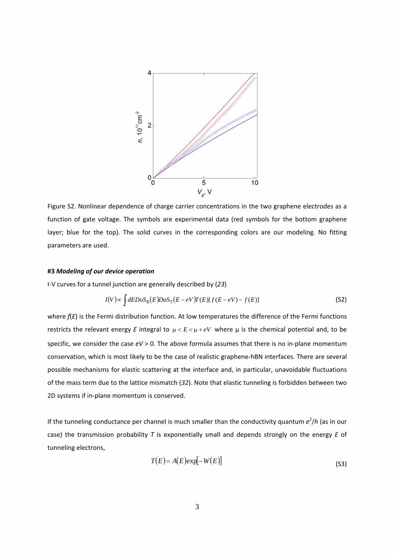
3
Figure S2. Nonlinear dependence of charge carrier concentrations in the two graphene electrodes as a
function of gate voltage. The symbols are experimental data (red symbols for the bottom graphene
layer; blue for the top). The solid curves in the corresponding colors are our modeling. No fitting
parameters are used.
#3 Modeling of our device operation
I‐V curves for a tunnel junction are generally described by (23)
)]()()[(TB EfeVEfETeVEDoSEDoSdEVI (S2)
where f(E) is the Fermi distribution function. At low temperatures the difference of the Fermi functions
restricts the relevant energy E integral to eVE where μ is the chemical potential and, to be
specific, we consider the case eV > 0. The above formula assumes that there is no in‐plane momentum
conservation, which is most likely to be the case of realistic graphene‐hBN interfaces. There are several
possible mechanisms for elastic scattering at the interface and, in particular, unavoidable fluctuations
of the mass term due to the lattice mismatch (32). Note that elastic tunneling is forbidden between two
2D systems if in‐plane momentum is conserved.
If the tunneling conductance per channel is much smaller than the conductivity quantum e2/h (as in our
case) the transmission probability T is exponentially small and depends strongly on the energy E of
tunneling electrons,
EWEAET exp (S3)

4
where A is a smooth function that depends on details of the wave‐function matching at the interface. In
our modeling, we assume A=const.
Let us now discuss some functional forms of W(E). For the case of an isotropic barrier, we need to solve
the dispersion equation zyxn kkkE ,, for each band of the barrier material, where E is the energy of
electrons tunneling in the z direction. No real solution for kz is possible inside the energy gap, and the
minimal Imkz zkIm for a given E and arbitrary kx and ky, which dominates the tunneling probability, is
given by
zkdEW Im2
For the case of parabolic bands,
mkz
2Im where Δ is the barrier height (in our case, the distance
to the valence band) and m is the effective mass (22,23,33).
In the case of layered crystals, their band structure can be described in the simplest approximation as
yxzzyx kkkkkk ,,, 1 (S4)
where (kz) =2tcos(kzl); t describes the interlayer coupling and l is the interlayer distance (for the case
of hBN, l 3.4Å). By solving the corresponding tunneling equation, we find kz within the gap to be
1
22ln
211
t
E
t
E
l
ikz
The top of the valence band corresponds to tkkE yx 2),(max 1max (to be specific, we choose t >0),
and the optimal value for the tunneling wavevector is then
11
21
2ln
1Im
2
ttlkz (S5)
where maxEE . If t2 , this expression can be simplified as
tl
ikz ln and yields the tunneling
probability T (t/Δ)2n where n =d/l is the number of atomic layers in the tunnel barrier. In the
opposite limit t2 , we obtain
*2mi
tl
ikz where
2
2*
2 ltm
is the effective mass in the
tunneling direction. This shows that the standard isotropic model is applicable to layered crystals,
provided the tunneling occurs not too far from the band‐gap edge.

5
Eq. (S4) is a simplified version of the real band structure of hBN, which depends on stacking order. hBN
crystals usually have AA’ stacking (34). In the next approximation that allows an analytical solution by
neglecting the mixing of π and σ bands (29,30), we obtain the following dispersion relation [S4]
yxzyxzg
zyx kkkkkkE
kkk ,2,4
,, 121
22
2 (S6)
where Eg is the energy difference between boron and nitrogen sites (34). In this case, we find
1
22ln
1Im
2
ttlkz (S7)
where yxg kk
EE ,
4 1
22 . Eq. (S7) differs from (S5) by replacement 4/22
gEEE , which
indicates the general validity of equation Imkz ln() for describing vertical tunneling through strongly
layered materials. (S5) and (S7) fit our experimental data equally well. It is worth noting that the
tunneling exponent through layered crystals depends on E only weakly (logarithmically) in comparison
with isotopic crystals that exhibit the standard square‐root energy dependence. For small changes in ,
this difference is unimportant (see below).
Finally, in the case of a strong electric field such that it changes the rectangular shape of the tunnel
barrier (Fig. 1D) the above expressions for W can be generalized within the WKB approximation (33) as
xkdxW z
d
Im20
.
#4 Layered versus isotropic barrier
In the main text, we have chosen for the sake of brevity to ignore the fact that our tunnel barriers are
made from a strongly layered material. This simplification allowed us to refer to the standard tunneling
theory. However, the assumption can be justified further by the fact that, for our device parameters,
we have found no difference between the I‐V characteristics calculated for the layered and isotropic
materials and, therefore, we cannot distinguish between the two cases. To illustrate the indifference to
the layered structure of our tunnel barrier, Figure S3 shows experimental I‐V curves for two devices and
compares them with the behavior expected for layered and isotropic cases. No major difference can be

6
seen, except at low bias in Fig. S3A. The exact shape of experimental curves at low bias varies from
sample to sample (cf. Fig. S3A & B) and, hence, we do not discuss the difference.
Figure S3. Tunneling I‐V characteristics for two different 4‐hBN‐layer devices at zero gate voltage and
their comparison with theory. (A) The red solid curve is the experimental data from Fig. 3. The two
dashed curves are our modeling for an isotropic barrier ( and m as in the main text) and for a layered
barrier of the same height and t =0.6eV, by using formulae from the above section. Note that t 0.6eV
corresponds to m =0.5m0. (B) Nominally similar device (for clarity, the experimental data are shown by
symbols). The curves are again the layered and isotropic versions of the tunneling theory. The fitting
parameter is the constant A in eq. (S3), which determines the absolute value of I. The close agreement
between functional forms of the theoretical curves validates the use of the conventional tunneling
formulae in the main text.
#5 Additional examples of our device operation
We have studied 6 multiterminal devices such as shown in Fig. S1 and >10 simpler tunneling FETs with
only one or two Ohmic contacts attached to each graphene electrode. The latter type does not provide
much information about the properties of the graphene electrodes but even one contact is sufficient to
study their tunneling I‐V characteristics. The devices with the same hBN thickness have exhibited
qualitatively similar behavior, as discussed in the main text. To illustrate the degree of reproducibility
for different samples, Figure S4 plots the behavior observed in another device with the tunnel barrier
consisting of 4 hBN layers. One can see that the nonlinear I‐V characteristics are qualitatively similar to
those presented in the main text, and their response to gate voltage is also similar.

7
Figure S4. Another hBN‐graphene‐hBN‐graphene‐hBN field‐effect device. (A) Tunneling I‐Vs and their
response to gate voltage (in 5V steps, cf. Fig. 3 of the main text). The inset compares the experimental I‐
V at zero gate voltage (red curve) with theory (dark) which takes into account the linear DoS in the two
graphene layers and assumes no momentum conservation.Temperature: 300 K. (B) Changes in low‐bias
tunneling (symbols) and the theory fit for 4 hBN layers (solid curve). The main difference with respect
to the device in the main text is a weak response at low gate voltages, which is probably due to
stronger disorder and chemical doping that smears the gate influence. The electron‐hole asymmetry
again implies the hole tunneling as discussed in the main text.
The only consistent difference that we noticed for a number of devices with 4 or more atomic layers of
hBN was the absolute value of T which could vary by a factor of 100 for nominally the same d.
Although this can be attributed to possible errors in determining the number of layers in thicker hBN
(26), more careful analysis of the devices’ response to bias and gate voltages reveals that the reason for
these variations is more likely to be inhomogeneous thickness of hBN. We believe that in some devices
one or two layers can be missing locally (in submicron scale patches) so that the tunnel current then
concentrates within these thinner areas. Graphite is known to cleave leaving occasional stripes of
smaller thickness for few‐layer graphene crystals and, whereas it is possible to see missing graphene
patches in an optical microscope, hBN does not allow the required resolution (26).

8
#6 Vertical transistors using few‐layer MoS2 as a barrier
One of the possible routes to increase the ON‐OFF ratio is to use materials with smaller . In this way it
would be viable to use thicker barriers but shift EF closer to the barrier edge, which should allow
exponential dependence of the tunnel current on gate voltage. One of the candidate materials is MoS2.
It is a layered semiconductor, which can be cleaved down to a monolayer (24). It has an indirect band
gap of 1.3eV (35), significantly lower than that in hBN. We have exploited MoS2 to prepare graphene‐
MoS2 devices by using the same procedures as described in the main text and in #1 of SOM.
I‐V characteristics for a transistor with a 6‐layer MoS2 barrier are presented in Figure S5A.
Measurements of its conductivity at a fixed small bias as a function of gate voltage are plotted in Fig.
S5B. The dependence is clearly exponential and in this device an ON‐OFF ratio of 10,000 has been
achieved. Further work is needed to improve the observed ratios further and to verify whether the
mechanism responsible for vertical transport through MoS2 is indeed tunneling.
Figure S5. I‐V characteristics of a graphene MoS2 device. Thickness of MoS2 is 6 layers. (A) ‐ Different
curves correspond to various gate voltages applied. Black: ‐40V; red: ‐20V; blue: 0V; purple: +20; green:
+40V. (B) ‐ Conductivity measured at a bias voltage of 0.2V as a function of gate voltage. The ON/OFF
ratio of >7103 is observed even for the relatively limited range of gate voltages.
Supplementary References
31. M. Bokdam et al., Electrostatic doping of graphene through ultrathin hexagonal boron nitride
films. Nano Lett. 11, 4631‐4635 (2011).

References and Notes 1. P. Avouris, Z. H. Chen, V. Perebeinos, Carbon-based electronics. Nat. Nanotechnol. 2, 605
(2007). doi:10.1038/nnano.2007.300 Medline
2. A. K. Geim, Graphene: Status and prospects. Science 324, 1530 (2009). doi:10.1126/science.1158877 Medline
3. F. Schweirz, Graphene transistors. Nat. Nanotechnol. 5, 487 (2010). doi:10.1038/nnano.2010.89
4. Y. Wu et al., High-frequency, scaled graphene transistors on diamond-like carbon. Nature 472, 74 (2011). doi:10.1038/nature09979 Medline
5. L. Liao et al., High-speed graphene transistors with a self-aligned nanowire gate. Nature 467, 305 (2010). doi:10.1038/nature09405 Medline
6. S. J. Han et al., High-frequency graphene voltage amplifier. Nano Lett. 11, 3690 (2011). doi:10.1021/nl2016637 Medline
7. Y. M. Lin et al., Wafer-scale graphene integrated circuit. Science 332, 1294 (2011). doi:10.1126/science.1204428 Medline
8. E. V. Castro et al., Biased bilayer graphene: Semiconductor with a gap tunable by the electric field effect. Phys. Rev. Lett. 99, 216802 (2007). doi:10.1103/PhysRevLett.99.216802 Medline
9. J. B. Oostinga, H. B. Heersche, X. Liu, A. F. Morpurgo, L. M. K. Vandersypen, Gate-induced insulating state in bilayer graphene devices. Nat. Mater. 7, 151 (2008). doi:10.1038/nmat2082 Medline
10. M. Y. Han, B. Ozyilmaz, Y. B. Zhang, P. Kim, Energy band-gap engineering of graphene nanoribbons. Phys. Rev. Lett. 98, 206805 (2007). doi:10.1103/PhysRevLett.98.206805 Medline
11. C. Stampfer et al., Transport in graphene nanostructures. Front. Phys. 6, 271 (2011).
12. D. C. Elias et al., Control of graphene’s properties by reversible hydrogenation: Evidence for graphane. Science 323, 610 (2009). doi:10.1126/science.1167130 Medline
13. S. Luryi, Quantum capacitance devices. Appl. Phys. Lett. 52, 501 (1988). doi:10.1063/1.99649
14. M. Heiblum, M. V. Fischetti, Ballistic hot-electron transistors. IBM J. Res. Develop. 34, 530 (1990). doi:10.1147/rd.344.0530
15. J. A. Simmons et al., Planar quantum transistor based on 2D–2D tunneling in double quantum well heterostructures. J. Appl. Phys. 84, 5626 (1998). doi:10.1063/1.368610
16. A. Zaslavsky et al., Ultrathin silicon-on-insulator vertical tunneling transistor. Appl. Phys. Lett. 83, 1653 (2003). doi:10.1063/1.1600832
17. A. Sciambi et al., Vertical field-effect transistor based on wave-function extension. Phys. Rev. B 84, 085301 (2011). doi:10.1103/PhysRevB.84.085301
18. Materials and methods are available as supporting material on Science Online.
1

2
19. C. R. Dean et al., Boron nitride substrates for high-quality graphene electronics. Nat. Nanotechnol. 5, 722 (2010). doi:10.1038/nnano.2010.172 Medline
20. A. S. Mayorov et al., Micrometer-scale ballistic transport in encapsulated graphene at room temperature. Nano Lett. 11, 2396 (2011). doi:10.1021/nl200758b Medline
21. K. S. Novoselov et al., Two-dimensional atomic crystals. Proc. Natl. Acad. Sci. U.S.A. 102, 10451 (2005). doi:10.1073/pnas.0502848102 Medline
22. L. A. Ponomarenko et al., Tunable metal–insulator transition in double-layer graphene heterostructures. Nat. Phys. 7, 958 (2011). doi:10.1038/nphys2114
23. R. V. Gorbachev et al., Hunting for monolayer boron nitride: Optical and Raman signatures. Small 7, 465 (2011). doi:10.1002/smll.201001628 Medline
24. A. H. Castro Neto, F. Guinea, N. M. R. Peres, K. S. Novoselov, A. K. Geim, The electronic properties of graphene. Rev. Mod. Phys. 81, 109 (2009). doi:10.1103/RevModPhys.81.109
25. J. G. Simmons, Generalized formula for the electric tunnel effect between similar electrodes separated by a thin insulating film. J. Appl. Phys. 34, 1793 (1963). doi:10.1063/1.1702682
26. E. L. Wolf, Principles of electron tunneling spectroscopy. Oxford University Press (1985).
27. L. A. Ponomarenko et al., Density of states and zero Landau Level probed through capacitance of graphene. Phys. Rev. Lett. 105, 136801 (2010). doi:10.1103/PhysRevLett.105.136801 Medline
28. J. M. Xue et al., Scanning tunnelling microscopy and spectroscopy of ultra-flat graphene on hexagonal boron nitride. Nat. Mater. 10, 282 (2011). doi:10.1038/nmat2968 Medline
29. N. Kharche, S. K. Nayak, Quasiparticle band gap engineering of graphene and graphone on hexagonal boron nitride substrate. Nano Lett. 11, 5274 (2011). doi:10.1021/nl202725w Medline
30. Y. N. Xu, W. Y. Ching, Calculation of ground-state and optical properties of boron nitrides in the hexagonal, cubic, and wurtzite structures. Phys. Rev. B 44, 7787 (1991). doi:10.1103/PhysRevB.44.7787 Medline
31. M. Bokdam, P. A. Khomyakov, G. Brocks, Z. Zhong, P. J. Kelly, Electrostatic doping of graphene through ultrathin hexagonal boron nitride films. Nano Lett. 11, 4631 (2011). doi:10.1021/nl202131q Medline
32. B. Sachs, T. O. Wehling, M. I. Katsnelson, A. I. Lichtenstein, Adhesion and electronic structure of graphene on hexagonal boron nitride substrates. Phys. Rev. B 84, 195414 (2011). doi:10.1103/PhysRevB.84.195414
33. L. D. Landau, E. M. Lifshitz, Quantum Mechanics. Oxford: Pergamon (1977).
34. R. M. Ribeiro, N. M. R. Peres, Stability of boron nitride bilayers: Ground-state energies, interlayer distances, and tight-binding description. Phys. Rev. B 83, 235312 (2011). doi:10.1103/PhysRevB.83.235312
35. Gmelin, Gmelin handbook of inorganic and organometallic chemistry (SpringerVerlag, Berlin, 1995).