Embed Size (px)
Citation preview

r
r
r
r
r
[
r
(
(
[
(
I
l
l
[
t
l
l
--------- UNCLASSIFIED ---------
NAVSHIPS 096 7-204-3010
TECHNICAL MANUAL
for
REPEATER, GROUP TELEGRAPH
AN/UGA-5
DEPARTMENT OF THE NAV Y
NAVAL EL ECTRONIC SYSTEMS COMMAND
------------ UNCLASSIFIED-----------
Publicativn: JULY 1966

Effective Pages UNCLASSIFIED NAVSHIPS 0967-204 -3010
AN/UGA-5
FRONT MATT ER
ii
PAGE NUMBERS
Title Page ii to v
1-0 to 1-5/1-6 2-1 to 2-3/2-4
LIST OF E FFECTIVE PAGES
CHANGE IN PAGE E FFECT NUMBERS
3-l to 3-2
4-l to 4-24 5- l to 5-23/5-24 6-l to 6-19/6-20
ST ELMA, Incorporated 200 Henry Street
Stamford, Connecticut
Contract: N600(63133)64773
N600(63133 )64926
CHANGE IN E FFECT
Errors found in this publication (other than obvious typographical errors) which have not been corrected by means of Temporary Changes or Permanent Changes should be reported on a user activity comment sheet NAVSHIPS 4914 (10-62) FSN 0105-503-9850. Such report should include the complete title of the publication and the publication number, identify the page and line or figure and location of the error, and be forwarded to the :=:ode 0523 of Naval Electronic S ystems Command.
All requests for this publication should be directed to the Naval Supply Depot, 580 l Tabor Avenue, Philadelphia 20 , Pennsylvania.
UNCLASSIFIED ORIGINAL
'1
,
1
1
'1
1
]
]
]
]
]
]
]
]
]
J
J
J

I'
r
r
r
r
I
(
[
(
(
(
l
l
(
l
t
l
t
AN/UGA-5
FRONT MATTER
UNCLASSIFIED
NAVSHIFS 0967-204-3010 Contents
Paragraph
TABLE OF CONTENTS
Page Paragraph Page
SECTION 1 - GENERAL INFORMATION SECTION 4 - TROUBLE SHOOTING
1-1 1-2 1-3 1-4 1-5
2-1 2-2 2-3
3-1 3-2
ORIGINAL
ScopP l-1 Description . . . . . . . . . . . . . . . . . . . 1-1 Refere�ce Data . . . . .... . . . . . . . . l-2 Equipment Supplied . . . . . . . . . . . • • l-4 Equipment, Materials, and
Publications Required But Not
Supplied. . . . . . . . . . . . . . . . . . . . . l-4
SECTION 2 - INSTALLATION
Unpacking and Handling . . . . . . . . 2 -l
I nstallation Procedures . . . . . . . . . 2-1 I nitial Checks . . . . . . . . . . .. . . . . . 2-2
SECTION 3 - OPERATION
Preparation for Use . . . . . . . . . . . . . 3-l
Operating Procedures . . . . . . . . . . . 3-l
4-l Logical Tr0uLl(: Shooting . . . . . . . . 4-l 4-2 Over-all runctwnal Description .. 4-l 4-3 Logic Anal','Sis . . . ... . . . . . . . . . . 4-4 4-4 Trouble Shooting Data . . . . ..... . 4-14
SECTION 5 - MAINTENANCE
5-l Failure, and Performance and
Operational Reports .... . . . . . . . 5-l 5-2 Preventive Maintenance ......... 5-l 5-3 Repair Procedures and Data . . . . . . 5-2
SECTION 6 - PARTS LIST
6-1 I ntroduction . . . . . . . . . . . . . . . . . . . 6-l 6-2 List of Assemblies . . . . . . . . . . • . . 6-l 6-3 Maintenance Parts List .......... 6-3 6-4 List of Manufacturers ...... 6-19/6-20
UNCLASSIFIED iii

Contents UNCLASSFIED NAVSHIPS 0967-204-3010
AN/UGA-5
FRONT MATTER
Figure
iv
1-1
2-1 2-2 2-3
2-4
3-1
4-1 4-2
4-2
4-3
4-4
4-5
4-6
5-1
5-2
LIST OF ILLUSTRATIONS
Page Figure Page
SECTION 1 - GENERAL INFORMATION
Repeater Group, Telegraph AN/UGA-5 l-0
SECTION 2 - INSTALLATION
AN/UGA-5, Rear View . • • . • . . . • . . . 2-l TH-73, Bottom View . • . . . . • • . , . • • . 2-2 Mark-Hold Strapping on Printed
Circuit Card A9 . . . . • • • • • . . . • . 2-3/2-4 Noise Switching Level Strapping on
Printed Circuit Card All • . • • . • 2-3/2-4
SECTION 3 - OPERATION
TH-73, Front Panel............... 3-2
SECTION 4 - TROUBLE SHOOTING
TH-73, Block Diagram • . . . . . . . • • • . 4-2 TH-73, Logic Diagram
(Sheet l of 2) ............... 4-5/4-6 TH-73, Logic Diagram
(Sheet 2 of 2) ............... 4-7/4-8 Synchronizing Technique for Phase
Bit Timing to the Mark/Space Transition of the Data . • . • • • • • • . . 4-10
Regenerated Data Displacement Diagram . . . . • . . . . . . . . . . . . . . • . . . 4-ll
Start/Stop Signal Synchronization Waveforms..................... 4-13
Start/Stop Signal Detection Logic • . 4-14
SECTION 5 - MAINTENANCE
Printed Circuit Cards Al and A2 (80060010) Component Location
Diagram . . • • • . • • • . . . . . . . • . . . • . • 5-3
Printed Circuit Cards Al and A2 Schematic Diagram • . . . . . . . • • • ,. . 5-4
5-3
5-4
5-5
S-6
5-7
S-8
5-9
Printed Circuit Card A3 (80060020) Component Location Diagram • . • • .
Printed Circuit Card A3 Schematic
Diagram • . • , . • . • . . • • • . • • • • • • . • •
Printed Circuit Card A4 (80060030) Component Location Diagram . • . • •
Printed Circuit Card A4 Schematic Diagram . . • . . . • . . . . • • . . . . • . . . • •
Printed Circuit Cards AS, A7, AlO, and Al3 (80060040) Component Location Diagram . . . • . . . • . . . . . . .
Printed Circuit Cards AS, A7, AlO, and Al3 Schematic Diagram . . . . . •
Printed Circuit Cards A6, A8, and Al2 (80060050) Component
5-5
5-6
5-7
5-8
S-9
5-10
Location Diagram . . . . . . . . . . . . . . . 5-11
5-10 Printed Circuit Cards A6, A8, and Al3 Schematic Diagram.......... 5-12
5-ll Printed Circuit Card A9 (80060060) Component Location Diagram..... 5-13
5-12 Printed Circuit Card A9 Schematic
Diagram....................... 5-14
5-13 Printed Circuit Card All (80060070) Component Location Diagram . . • . . 5-15
5-14 Printed Circuit Card All Schematic Diagram • • . • • . • . . • . • . • • • • • • • . . . 5-16
5-15 Printed Circuit Card Al4 (80060080) Component Location Diagram . . • • • 5-17
5-16 Printed Circuit Card Al4 Schematic Diagram • • • • • . . . • • . . . . • • . • • • . . . 5-18
5-17 Printed Circuit Card AlS (80060090) Component Location Diagram . . • . • 5-19
5-18 Printed Circuit Card AlS Schematic
Diagram • . • • • • • . • • . . • • • • • • • • • • . 5-20 5-19 Wiring Diagram for Rack Shelf
Adapter • • • • • . • • • . . . • . • • , . • 5-21/5-22 5-20 Wiring Diagram for TH-73 • • • • • 5-21/5-22 5-21 Parts Location Diagram for
TH-73 . . . • . . . . . • . . . . . . . • . • . 5-23/5-24
UNCLASSIFIED ORIGINAL
..
··.···) .
1
1
l
;1
"1
]
]
]
]
]
l
]
J .
J
J
J
J

I
r
r
r
r
r
I
I
(
(
(
l
l
(
[
l
l
t
AN/UGA-5 FRONT MATTER
UNCLASSIFIED NAVSHIPS 096'1-204-3010
Contents
LIST OF TABLES
Table Page
SECTION 1 - GENERAL INF ORMATION
1-1 Printed-Circuit Card Distribution . . . . 1-2
1-2 Equipment Supplied ............... 1-4
1-3 Equipment, Materials, and Publications Required But Not Supplied • . • . . • • • . . • . . . . . . . . . . . . • 1-4
SECTION 3 - OPERATION
3-l Controls, Indicators, and Jacks . . • . . 3-l
SECTION 4 - TROUBLE SHOOTING
4-1 TH-73 Trouble Shooting Chart . . . . . . . 4-16
4-2 Frequency at Various Test-Points . . . . 4-20
4-3 General Logic-Circuit (PNP Transistors) Trouble Shooting Chart . . • . . . . . . • • . • . . . . . . • • . • • . • 4-22
Table Page
4-4 General Logic-Circuit (Using NPN Transistors) Trouble Shooting Chart . . . • • . • . . . . . • . . • . . . . • • . . . . 4-23
4-5 Diode AND-Gate Trouble Shooting Chart . . . • • • . • . . . • . . . . . • . • • • . . . . 4-23
4-6 Bistable Trouble Shooting Chart . . . • • 4-23
SECTION 5 - MAINTENANCE
5-1 Test Equipment and Material Required for Preventive Maintenance . • . • . . . . 5-l
SECTION 6 - PARTS LIST
6-l List of Assemblies . . . . • . • . • • . . . . . • • 6-2
6-2 Repeater Group, Telegraph AN/UGA-5 Maintenance Parts List • . • • . . • . . • . 6-3
6-3 List of Manufacturers . . . . • • . • • 6-19/6-20
O RIGINAL UNCLASSIFIED v

Figure 1-1
1-0
UNCLASSIFIED NAVSHIPS 0967-204-3010
Repeater, Regenerative TH-73
Figure l-l. Repeater Group, Telegraph AN/UGA-5
UNCLASSFIED
AN/UGA-5 FRONT MATTER
ORIGINAL
'1
l
1
1
1
?1
']
]
]
]
]
•1 ,�,
]
J
J
J
J
J

r
r
r
r
I
r
(
('
I
(
(
I
(
l
l
l
l
t
t \
AN/UGA-5 GEJ'JERAL INFORMATION
UNCLASSIFIED NAVSHIPS 0967-204-3010
Paragraph l -1
SECTION l
GENERAL INFORMATION
1-l. SCOPE.
This manual describes Regenerator Repeater Group, Telegraph AN/UGA-5 (see figure 1-l), hereafter referred to as AN;UGA-5, and prov1des the information required for its installation, operation, and maintenance. This Technical Manual is in effect upon receipt. Extracts from this publication may be
made to facilitate preparation of other Department of Defense publications.
l-2. DESCRIPTION.
a. FUNCTIONAL.- The AN/UGA-5 provides facilities for (l) signal regeneration on four synchronous channels (at one of four modulation rates: 37.5 bauds, 61.1 bauds, 75 bauds, and 150 bauds) or on four start-stop channels (at one of three modulation rates: 45.5 bauds, 74.2 bauds, and 75 bauds). Although any code-level may be used for synchronous channels, start-stop operation allows
use in systems employing only 5-, 6-, 7-, or 8-level codes. The AN/UGA-5 regenerates signals contain
ing up to 45 per cent distortion and produces output signals that contain a maximum of up to 1 per cent distortion. The AN/UGA-5, which may be used on channels carrying synchronous and start-stop signals, automatically switches from one mode to the other according to the type of incoming signal.
(l) Since output signals are provided through an electronic relay, a supply battery is required locally or at the receiving station.
(2) The input and output circuits permit high-level keying (260-volt de, 20- or 50-milliampere, neutral; or ±130-volt, 3 a-milliampere polar), as well as low-level keying (±6-volt polar) for compatibility with interface requirements of associated military standards (MIL-STD-1888).
(3) False-start protection prevents production of an output signal when noise-pulses up to l /2-bit are developed on the line during character stop- and rest-Mark intervals.
(4) An automatic mode-control circuit detects the type of incoming data, and establishes the equipment's mode of operation accordingly so that output data is the same type as the input data.
(5) An automatic disconnect circuit inhibits the output and places a steady Mark on the line when an incoming synchronous signal is lost.
(6) Provision is made for on-line testing of each of the four channels. b. PHYSICAL.- The AN/UGA-5 comprises four Regenerative Repeaters, Automatic TH-73/UGA-5
(hereafter referred to as TH-73) enclosed in a rack shelf adapter (see figure l -1) that can be mounted in a 19 -inch equipment rack or cabinet.
(1) Each TH-73 plugs into a separate receptacle (mounted on the inside at the rear of the rack shelf adapter), through which it receives all necessary inputs (power and signal); each receptacle is connected to a terminal strip mounted on the back of the rack shelf adapter, to which all external connections are made. Incoming power connections to the AN/UGA-5 are also made to a terminal strip on the rear of the rack shelf adapter.
(2) Test connections for in-line testing of each channel are provided on the front panel of each TH-73.
(3) All operator controls, and the fuse, are mounted on the front panel of the TH-73. (4) Each TH-73 contains 17 plug-in assemblies. Assemblies Al through A l 5 are printed
circuit cards, and A l6 and A l 7 are sealed units. Table l -1 enumerates the reference designations and distribution of PC assemblies employed.
ORIGINAL UNCLASSIFIED 1-l

Table l-1
UNCLASSIFIED NAVSHIPS 0967-204-3010
AN/UGA-5 GENERAL INFORMATION
TABLE 1-1. PRINTED-CIRCUIT CARD DISTRIBUTION
PRINTED-CIRCUIT ASSEMBLY
DESIGNATION A1
A2 A3 A4 AS
A6
A7 AS A9 A10 All Al2
A13
A l 4 A15
1-3. REFERENCE DATA.
The following reference data is applicable to each of the four TH-73 units mounted in the AN/UGA-5.
a. INPUT SIGNAL. (l) Mode
(2) Rate
(3) Code (strap-selectable)
{4) Type (strap-selectable)
(5) Current (strap-selectable)
MATING HARNESS-BOARD CONNECTOR
DESIGNATION XA1 XA2 XA3 XA4 XA5 XA6 XA7 XA8 XA9 XA10 XA11 XA12
XA13
XA14 XA15
Synchronous or start-stop; either type may be switch-selected or automatically selected as determined by front-panel Mode switch setting. Four internal combinations. (Rates are selected by setting of switch accessible through hole in front panel (screwdriver adjustment); corresponding baud-rates are automatically selected by mode (start-stop or synchronous) of received data-signal.)
37.5-baud synchronous, 45.5-baud start-stop (60 words per minute, nominal).
61. 1-baud synchronous, 74. 2-baud start-stop (100 words per minute, nominal).
Combination 75-baud synchronous and 75-baud start-stop.
150-baud synchronous.
(If required, other rates and/or more precise timing may be obtained from an external source.) 5-, 6-, 7-, or 8-level (7-, 8-, 9-, 10-, or 11-unit) start-stop code; any unit-interval synchronous code. High-level 260-volt de neutral, or ±130-volt polar; low-level ±6 volts (per MIL -STD-188B). Input loop de-isolated from ground. High-level, 20- or 50-milliampere neutral. (90 milliampere maximum at the high level input.)
1-2 UNCLASSIFIED ORIGINAL
�1
,
1
l
l
1
]
l
]
]
]
,)
]
]
J
J
J
J
I

I
r
r
r
('
[
f
I'
I
I
(
l
(,
l
I
l
1
[
J
AN/UGA-5 UNCLASSIFIED NAVSHIPS 0 967-204-3010
POJ.ragraph 1-3a (6) GENERAL INFORMATION
(6) Distortion (7) Impedance
(8) Sensitivity
b. OUTPUT SIGNAL.
( 1) Type
(2) Current
(3) Distortion (4) Impedance
c. TIMING. ( l) Internal
(2) External
(3) Send and Receive equipment
d. SYNCHRONIZATION. (l) Correction increment (2) Timing
e. MODES OF OPERATION.
( l ) Automatic
(2) Manual
f. MARK-HOLD OPTION (Strap-Selectable) start-stop operation only.
g. FALSE-START PREVENTION (start-stop operation only).
h. NOISE-SWITCHING THRESHOLD (strap-selectable).
i. RADIO FREQUENCY INTERFERENCE (RFI) SUPPRESSION.
45 per cent total Marking or Spacing distortion.
100 ohms nominal for 60-milliampere (rna) operation and 300 ohms nominal for 20ma operation, which are provided by internal strapping. Input signal variation of 2ma above or below the average current.
High-level 2 60-volt de neutral or 130-volt de polar; low level ±6 volts (per MIL-STD-1888). Output loop de-isolated from ground. Highlevel, 20- or 60-ma neutral or polar; lOOma maximum (continuous duty).
Less than l per cent at maximum keying rate. Less than 200 ohms when the output is in the Marking or closed circuit condition.
Oscillator-supplied frequencies of 76.8kc, 93.237kc, 125.217kc, or 152.016kc. MIL-STD-1888 input required. Frequency must be 256 times bit-rate. For example: bit-rate= 150 baud, frequency of external oscillator must be 38. 4kc.
Synchronization of equipment clocks at send
and receive points is mantained for a period up to 30 minutes, with up to three TH-73 units connected in tandem between the send and receive ends of a communications link, after the input data is removed and reconnected within the 30-minute period.
1 part in 12 8 of bit. 12 8 times bit-timing derived from internal clock. Automatically switches to regenerate start-stop signals on detection of: (a) long Mark ( 1-second duration or longer); (b) start-stop data-pattern within 50 characters; (c) detection of start-stop rate selected. Automatically switches to regenerate synchronous data-signals on detection of absence of start-stop signals (distinguished by missing Mark rest-pulse segments). Regenerates either synchronous or start-stop signals (separate switch selects synchronous or start-stop mode, when in the manual Mode select switch position). When connected by strapping, a Mark is produced at the end of each character and maintained for the duration of the stop-Mark interval, regardless of the input signal during that time.
Prevents start of operation when noise-pulses up to 1/2-baud in duration are developed on the line. Determines level of noise switching.
Meets all limits specified in MIL-I- 1691 OA. In addition, the radiated interference level does
ORIGINAL UNCLASSIFIED l-3

Paragraph 1-3j
UNCLASSIFIED NAVSHIPS 0967-204-3010
AN/ UG A-5 G ENERAL INFORMATION
j • POWER REQUIREMENTS.
k. OPERATING TEMPERATURE RANGE. 1. DIMENSIONS.
not exceed l microvolt per meter per kilocycle of bandwidth (measured at a distance of 3 feet in all directions), nor does the conducted interference level exceed l microvolt per kilocycle of bandwidth over the range of frequencies specified in MIL-I-16910A.
120 volts ±10 per cent at SU or bU cycles per second ±5 per cent, 20 watts. 0 to 50 degrees centigrade. 5-1/4 high, 4-1/4 wide, and 20 inches deep. (Four units mounted abreast in 19-inch rack shelf adapter.)
m. WEIGHT. 8 pounds (AN/UGA-5, 41 pounds).
1-4. EQUIPMENT SUPPLIED.
Table 1-2 lists equipment supplied as Repeater Group, Telegraph AN/UGA- 5.
TABLE 1-2. EQUIPMENT SUPPLIED
QTY PER NOMENCLATURE COMMON OVER-ALL VOLUME
EQUIP. NAME DESIGNATION NAME (DIM. (IN.) (CU FT)
1 Repeater Group, Tele- AN/UGA-5 AN/UGA-5 5-1/4 high 0.32 graph 4-1/4 wide
20 deep
Technical Manual for NAVSHIPS - 11 high
Repeater Group, Te1e- 0967-204- 8 -1/2 wide
graph AN;UGA-5 3010 3/4 thick -------· 1-5. EQUIP:viENT, MATERIALS, AND PUBLICATIONS REQUIRED BUT NOT SUPPLIED.
WEIGHT (LB)
41
Table 1-3 lists equipment, materials and publications required but not supplied as a part of the
AN/UGA-5.
QTY PER
EQUIP
l
1
1
1
1
1-4
TABLE i -3. EQUIPMENT, MATERIALS, AND PUBLICATIONS REQUIRED BUT NOT SUPPL IED
NOMENCLATURE
NAME DESIG NATION REQUIRED USE
Oscilloscope AN/USM-1 05A Trouble shooting and maintenance
Electronic Multimeter AN/USM-116 Trouble shooting and maintenance
Multimeter AN/PSM-4(C) Trouble shooting and maintenance
Frequency Counter AN/USM-207 Testing and adjustment procedures
Transistor Test Set AN/USM-206 Trouble shooting and maintenance
UNCLASSIFIED ORIGINAL
�1
1
1
1
1
1
]
]
')
]
]
]
]
]
J
J
J
J
J

I
r
r
r
(
('
('
r
I
(
I
(
(
I
(,
l
L
t
t
AN/UGA-5 GENERAL INFORMATION
UNCLASSIFIED NAVSHIPS 09 67-2 04-30 l 0
QTY PER
EOUIP
TABLE l -3. EQUIPMENT, MATERIALS, AND PUBLICATIONS REQUIRED BUT NOT SUPPLIED (CONT'D)
NOMENCLATURE
NAME DESIGNATION REQUIRED USE
Table l-3
2 Power Resistor 2000 ohms, Current limiting for 20-ma loop operation and l 0 watts testing
l Test Set, Telegraph AN/GGM-1 Testing and adjustment
l 130-Volt Polar Loop PP-351 Maintenance Supply
l Technical Manual for Navships 0280-Electronic Multimeter 667-7005 AN/USM-116
l Technical Manual for Navships 92051 Multimeter AN/PSM-4(C)
l Technical Manual for Navships Oscilloscope 93658A AN/USM-1 OSA
l Technical Manual for TMl l -2698* Frequency Counter AN/USM-207
l Technical Manual for Navships 0969-Transistor Test Set 002-7011, 7020 AN/USM-206
l Technical Manual for Navships 94244 Test Set, Telegraph AN/GGM-1
*Dept. of the Army Technical Manual
ORIGINAL UNCLASSIFIED l -5/l -6


I r r [ r I I I I ( l I I 1 1 l I t L
AN/UGA-5 INSTALLATION
UNCLASSIFIED NAVSHIPS 0967-204-3010
Paragraph 2-l
SECTION 2
INSTALLATION
2-1. UNPACKING AND HANDLING.
Exercise normal care when unpacking the contents of the shipping case. Inspect the equipment for evidence of any damage incurred in shipment and handling.
2-2. INSTALLATION PROCEDURES.
a, SITING AND INSTALLATION.- The AN/UGA-5 must be located in an area accessible to operating personnel and where 115-volt ac power is available.
(1) Provide a mounting facility that accommodates the physical dimensions of the AN/UGA-5.
(2) Set the AN/UGA-5 into the mounting facility, and secure the unit in position. b. CONNECTIONS.- Make all required signal and power connections at the rear of the unit,
as indicated in figure 2-1. Incoming power connections are made to terminal board TB5; external timing connections to the respective units are made at terminal boards TB1 through TB5.
WARNING HIGH VOLTAGE
T85 Pl WER
rhg r "'' '""'
T84
� EXT TIMING
-SIG} {SIG--GRD
SYNC GRD-
-SIGJ S/S -[SIG--GRD GRD-
c::r=J -IN- r:= - + j E+--+ -OUT- :=
T83 T82
\\ --:\
0 0
--- J 0
Figure 2-1. AN/UGA-5, Rear View
c. ST RAPPING OPTIONS.
EXT TIMING
-SIG} {SIG-SYNC
-GRD GRD--SIG} S/S {SIG--GRD GRD-
=: j- OUT- E: =
T81 r-:::
(l ) INPUT SIGNAL.- Before operating the AN/UGA-5, strap for the input signal to each TH-73 as described below.
(a) Obtain access to the bottom of the TH-73 by unscrewing the chassis lock-screw (located in the center at the bottom of the front panel) and sliding the unit out of the rack shelf adapter.
(b) Locate the strapping terminals on the bottom of the chassis (see figure 2-2). (c) Select the terminals for the desired operating loop conditions, and strap as follows:
!. For 20-ma loops, connect and solder terminal E3 to E4 •
.f. For 60-ma loops, connect and solder terminal E4 to E5. l For neutral loops, leave terminals El and E2 open. ! For polar loop and low-level (±6V) signal, connect and solder terminal El to E2.
ORIGINAL UNCLASSIFIED 2-1

F1gure 2-2
UN CLASSIFIED NAVSHIPS 0967-204-3010
UNIT CODE STRAPPING
AN/UGA-5
INSTALLATION
FRONT PANEL INPUT STRAPPING TERMINALS
SPARE FUSE
XA�I· + + +
� �
�
30+ + + oz
+ + _.fAI5
+�+ + + + + + + + + + � � + +
XAI7
y 8:� 0" E5 E4E3E2E 0000
TP6
0@ X
AI& OXCI
TMC.S'�DZ.OOT
Figure 2-2. TH-73, Bottom View
(2) MARK-HOLD.- To include the Mark-hold provision, strap terminals 2 and 3 (see figure 2-3). When the Mark-hold is not desired, strap terminals l and 2,
(3) UNIT CODE.- Select the desired unit code, and strap as indicated below, using figure
2-2 as guide. (a) For 5 -unit code, connect and solder terminal I to 2, and terminal 4 to 5, (b) For 6-unit code, connect and solder terminal I to 3, and terminal 4 to 5. (c) For 7 -unit code, connect and solder terminal 4 to 2, and terminal l to 5. (d) For 8-unit code, connect and solder terminal 4 to 3, and terminal l to 5.
(4) NOISE SWITCHING SENSITIVITY,- To provide a decrease in the probability of noisepulses switching the equipment's mode of operation from synchronous to start-stop, strap terminal l to 2 on printed-circuit card A l l (see figure 2-4). When noise will not interfere with switching (on lines employing start-stop signals only or on low noise lines), strap terminal 2 to 3.
2-3. INITIAL CHECKS,
a. Before power is applied to the AN/UGA-5, check that the proper fuses are installed in the fuse holders on the front panels. Assure that all printed-circuit cards are securely seated in their respective harness-board receptacles. Check that all rear connections are properly installed, observing correct signal polarity.
2-2
b, After power is applied:
(l) Check that POWER indicator lamp lights.
(2) With signal applied, check that SIGNAL indicator lamp reacts appropriately.
Note
If proper indications are not obtained, refer to Section 4.
UNCLASSIFIE D ORIGINAL
1 1 1 1 �') l ] '1 ] ] ] ] ] ] J ] J J J

I
f
I
l
r
I
I
I
I
l
l
l
1
l
I
1
(
(,
l
AN/UGA-5
INSTALLATION
ORIGINAL
UN CLASSIFIED
NAVSHIPS 0967-204-3010
2 3 0 0
I 0
TM�,ti S�Ci.GC2
..____
r--
Figure 2-3. Mark-hold Strapping On Printed Circuit Card A9
2
10
0 3 0
'-----
r--
TM-R-5,02004-
Figure 2-4 • . Noise Switching Level Strapping On Printed Circuit Card All
UNCLASSIFIED
F igure
2-3
2-3/2-4


r
r
r
r
r
r
(
r
(
[
I
I
[
1.
(,
t
L
t
t
AN/UGA-5 OPERATION
UNCLASSIFIED NAVSHIPS 0967-204-3010
Paragraph 3-1
SECTION 3
OPERATION
3-1. PREPARATION FOR USE.
After the AN/UGA ·5 is set up for operation in accordance with Section 2 of this manual, no further preparation or setup procedures are required except when an external timing source (oscillator) is to be used to obtain the upper range of output bit-rates. C onnection of this external oscillator is effected by connecting to the EXT TIM ING IN terminals at the rear of the rack shelf adapter (see figure 2-1) .
3-2. OPERATING PROCEDURES.
a. DESCRIP TION OF CONTROLS.- Table 3-1 lists TH-73 operating controls and indicators (see figure 3-1) and provide descriptive and functional information for each.
TABLE 3-1. CONTROLS, INDICATORS, AND JACKS
PANEL IDENTIFICATIONI DESCRIP TION
SIG NAL I Indicator lamp, yellow
RATE,BAUDS I 5-position rotary switch, screwdriver turn
MODE 2-position toggle switch
MANUAL 2-position toggle switch
PHASE 2-position toggle switch
FUNC TION
Lights when input signal is in a M ark condition; flashes during normal traffic.
When set to 60wpm (37. 5-45. 5), 100 wpm (61.1-74.2), 75 - 75 baud, or 150 baud, the TH-73 accepts start-stop or synchronous signals at the designated rate. (When set to EXT, other rates may be obtained from an external timing source.)
When set to:
(1) AUTO, TH-73 regenerates start-stop or synchronous signals automatically.
(2) MANUAL, the MANUAL switch (listed below) is enabled.
Operative when MODE switch is set to MANUAL. When MANUAL switch is set to:
(1) S/S, TH-73 regenerates only start-stop signals.
(2) SYNC, TH-73 regenerates only synchronous signals.
Sets the time for bit-synchronization (synchronous mode only) . When set to:
(1) NORM, causes TH-73 to be within 10 per cent of ideal synchronization by the time
ORIGINAL UNCLASSIFIED 3-1

Table
3-1
UN CLASSIFI ED NAVSHIPS 0967-204-3010
AN/UGA-5 OPERATION
TABLE 3-l . CONTROLS, INDICATORS, AND JACKS (Cant 'd)
PANE L IDENTIFICATION DESCRIPTION FUNCTION
approximately 1000 M/S transitions have been received at the input.
(2) RAPID, causes TH -7 3 to be within 2 per cent of ideal synchronization by the time approxi
mately 64 M/S transitions have been re
ceived at the input. (These are the specification values for normal and rapid times for
bit synchronization. Corresponding factory tested values are 64 and 5 6, respecr tively.)
IN Test jacks, white and
black
Permit oscilloscope connection, to check
input signal.
OUT rest jack, white and
black
Permit oscilloscope connection, to check
regenerated output signal.
POWER
3/4 AMP
2-position toggle switch
Indica tor lamp , red
Fuse
Controls application of ac power to the repeater.
Lights when ac power is applied to the repeater.
AC line fuse indicator-type: red button
indicates blown fuse.
b. SEQU ENCE OF OPERATION.- Set front-panel controls to the desired mode of operation, apply power, and check that
POWER lamp lights. Operation from this point on is automatic unless the manual mode of operation is in effect (i.e. , MODE switch set to MANU AL), in which case the MANUAL switch m ust be set to the position appropriate for the type of incoming signal.
c. OPERATOR'S MAINTENANCE. (l) PREVENTIVE MAINTENANCE.- Refer to Section 5
of this manual for preventive maintenance information.
(2) EMERGENCY MAINTENANCE.- In the event the AN/UGA-5 fails when continued operation is of paramount
importance, the operator may resort to the following emergency
procedure to attempt to restore operation:
(a) Check that POWER indicators on all TH-73 units light. If all of them are out, check for 115 volts at the appropriate terminals on terminal board TBS at rear of rack
shelf adapter (see figure 2-l ); if voltage is not present, check power source. If correct voltage is present, check front-panel fuse. If fuses are good, proceed to step (d), below.
(b) Check for SIGNAL lamp indication when
signal is applied. If correct indication is not obtained, use multimeter or oscilloscope to check for signal at signal IN test
!H- - l UGA-�
� - ''iii'· •
\l
points on front panel. If no signal is present, replace assem- Figure 3-l. TH-7 3, Front Panel
bly Al6. If signal is present, proceed to step (d), below.
(c) Check for signal at front-panel signal O U T test-points. If signal is present, replace
assembly Al7. (d) If the above procedures have failed to restore the TH-73 to operating condition,
refer the unit to a maintenance technician.
3-2 UNCLASSIFIED ORIGINAL
]
,
1
1
l
1
l
]
]
]
]
]
J
J
J
J
J
J
I •

r
r
r
r
r
r
(
(
(
[
[
[
(
l
[
t
t
l
l
AN/U GA-5
TROUBLE SHOOTING
4-l . LOGICAL TROUBLE SHOOTING.
UNCLASSIFIED
NAVSHIPS 09 67-204-3010
SECTION 4
TROUBLE SHOOTING
Paragraph
4-1
This section contains information to aid in quickly and efficiently determining the cause of equipment malfunction. The information is given in order of over-all trouble shooting technique, operation
al data (functional and logical) 1 and trouble shooting data.
a. SYMPTOM RECOGNITION. - This is the first step in the trouble shooting procedure and is
based on a complete knowledge and understanding of equipment operating characteristics. All equipment troubles are not necessarily the direct result of component failure. Therefore, a trouble in an
equipment is not always easy to recognize since all conditions of less than peak performance are
not always apparent. This type of equipment trouble is usually discovered while accomplishing
preventive maintenance procedures. It is important that the "not so apparent" troubles, as well as
the apparent troubles 1 be recognized. b. SYMPTOM EL ABORATION.- After an equipment trouble has been "recognized, " all the
available aids designed into the equipment should be used to elaborate, further, on the original
trouble symptom. Use of front-panel controls and other built-in indicating or testing aids should
provide better identification of the original trouble symptoms. Also, checking or otherwise manipula
ting the operating controls may eliminate the trouble. c. LISTING PROBABLE FAULTY FUNCTION.- The next step in logical trouble shooting is to
formulate a number of "logical choices" as to the cause and likely location (functional section) of the trouble. The "logical choices" are mental decisions which are based on knowledge of the equipment
operation, a full identification of the trouble symptom, and information contained in this manual.
The over-all functional description and its associated block diagram should be referred to when
selecting possible faulty functional sections. , d. LOCALIZING THE FAULTY FUNCTION.- For the greatest efficiency in localizing trouble, the
functional sections which have been selected by the "logical choice" method should be tested in an order that will require the least time, This requires a mental selection to determine which section to test first. The selection should be based on a further extension of the "logical choice" method. If tho tests do not prove that functional section to be at fault, the next section should be tested, and
so on until the faulty functional section is located. As aids in this process, this manual contains a
functional description and a servicing block diagram for each functional section. Waveforms are
included at significant check points on servicing block diagrams to aid in isolating the faulty section.
Also 1 where applicable, test data (such as information on control settings, critical adjustments, and
requires test equipment) are supplied to augment the functional description and servicing block
diagram for each functional section.
e. LOCALIZING TROUBLE TO THE CIRCUIT.- After the faulty functional section has been
isolated 1 it is often necessary to make additional "logical choices" as to which group of circuits or
circuit (within the functional section) is at fault. Servicing block diagrams for each functional
section provide the signal-flow and test-location information needed to bracket and then isolate the
faulty circuit.
f. FAILURE ANALYSIS.- After the trouble (faulty component, etc.) has been located (but prior to
performing corrective action) 1 the procedures followed up to this point should be reviewed to determine exactly why the fault affected the equipment in the manner it did, This review is usually necessary to make certain that the fault discovered is actually the cause of the malfunction, and not
just the result of the malfunction.
4-2. OVER-ALL FUNCTIONAL DESCRIPTION (see figure 4-1).
a. GENERAL.- The TH-73 consists primarily of a synchronous {sync) regenerative repeater and a start-stop (s/s) regenerative repeater, together with mode-decision and -switching mechanisms
ORIGINAL UNCLASSIFIED 4-l

Figure
4-l
DATA IIJPUT
EXT TIM IN sou
INPUT INTERFACE
{SYNC A L R:;,ES
RATES
INPUT DATA LINE
OSCIL L ATOR � 76 8KC f--
93.Z37 KC f-125.217KC 152.016KC
EXTERN IlL �- ';{_ INfERFACE
IRATE BAUDSI
UN CLASSIFIED
NAVSHIPS 097-204-3010
INPUT DATA LINE
ADD-SUBTRt>LT
LOGIC AUTCI'<1ATIC
DISCONNEC T LOGIC
SIGNAL BIT TIMING BIT TIMER
RESET 128 X BAUD RATES
S/S START/ TIME AUTOMATIC STOP BA SE MODE '-----CHAR. ENERATOR
SYNC CONTROL CONTROL
I NPUT DATA LINJ: l J
DATA REGEh-
ER A TOR
OUTPU;r'. INHIBIT
A N/UGA-5
TROUBLE SHOOTING
OUTPUT INTERFACE
RE GENERATEDLlATA OUTPUT
TMI!>SOtJZr,o&
Figure 4-l . TH-73, Block Diagram
that provide automatic or manual control for signal regeneration. The following paragraphs describe
their operation in regenerating synchronous and start/stop signals; a discussion of the switching from start-stop synchronous and from synchronous to start-stop is also included,
b. SYNCHR ONOUS OPERATION.
(l) Input data is applied to the input interface where it is converted to logic-level signals
and developed on the input data line, These logic-level signals are fed to all TH-73 circuits except
the timing circuits.
(2) The timing signal is generated in an oscillator whose frequency is chosen on the basis
of the incoming signal's baud-rate and mode (start-stop or synchronous). This output frequency
(76.8kc, 93.23kc, l 25.2l kc, or l 52.016kc) is then fed to the time-base generator, where it is
counted down to a rate 128 times that of the incoming signal. (3) The add-subtract logic operates automatically, in conjunction with the signal bit-timer,
to produce and maintain correct phasing. An incoming Mark-to-Space (M/S) data transition is
compared to the internal clock-signal (bit-timing from signal bit-timer). If these two signals match in time, the internal clock is in proper phase. If they do not match, add-subtract logic determines
whether the internal clock is to be advanced or retarded: when the internal clock is to be advanced in time, clock-pulses are added (inserted into the time-base output); for retardation, clock-pulses are
subtracted (deleted) from the time-base output.
(a) If initial phasing is incorrect, each M/S data-transition produces a 1/128 of a bitinterval correction and the clock shifts its timing until correct phasing is realized. Thereafter,
alternate add and subtract pulses are generated to maintain correct phasing, (b) The frequency-error between the synchronous data-rate and the internal time-base
is automatically corrected for by add-subtract logic. When the correct phase is reached, the
frequency-error appears as a slow-changing phase-difference between the data-transitions and the
internal clock-signals, in the process of obtaining correct phasing. Consequently, add-subtract logic generates add- or subtract- pulses, as required, to correct the slow phase-change. Therefore,
when the error accumulates to one clock-pulse at the input to add-subtract logic, it is corrected for by
a phase-adjustment of 1/128 of a bit. (c) For every M/S data-transition, early or late, a pulse is subtracted. When the
M/S data-transition is early with respect to bit-timing, two pulses (one pulse added to second stage of the chain) are also added, giving a net effect of adding one pulse; when the transition is late, no pulses are added, and the net result is the subtraction of one pulse, This sequence forces bit-timing to move into phase with M/S data-transitions.
4-2 UNCLASSIFIED ORIGINAL
1
,
,
l
1
l
''1
1
]
]
]
]
]
]
J
J
J
J
J

r
r
r
r
r
r
r
(
[
[
[
1
l
l
t
l
l
l
l
A N /UGA-5 TROUBLE SHOOTING
UNCLASSIFIED NAVSHIP S 0967-204-3010
P aragraph
4-2b(4)
(4) The in-phase bit-timing is applied to the data regenerator and to automatic-disconnect
logic.
(a) As it is applied to the data regenerator, the positive-going edge of the timing signal is lined up with an M/S transition of the incoming data. The negative-going transition of the timing signal (one cycle per bit) occurs at the mid-point of an ideal data-signal bit -- the optimum point for signal-bit sampling. The incoming data sets the data regenerator, and the bit-timing pulse allows the incoming data to be sampled. The data regenerator then changes the output signal to conform to the input signal {1/2-bit delayed), thereby regenerating the incoming data with less than l
per cent distortion. (b) Bit-timing is also applied to the automatic-disconnect logic, where the output is
inhibited and a steady Mark is produced when no transitions exist at the input for a 32 bit-time
period. The output remains inhibited for 63 bit-times after resumption of incoming data, allowing the TH-73 to synchronize before applying the regenerated data to the output line.
(c) Synchronization between send and receive clocks at the respective ends of a communications link is maintained even though the link is interrupted. Synchronization is maintained for
a period up to 30 minutes with an absence of data on a link containing up to three TH-73 units in tandem. Once synchronization is established, data can be removed and replaced within the 30-minute period, without loss of synchronization.
c. START/STOP OPERATION.- In this mode, TH-73 operation is essentially the same as for synchronous operation except that, instead of establishing phase-position by addition and subtraction of pulses, character-framing is used to eliminate biasing distortion. Furthermore, a start/stop-character control is added to the circuits, and the automatic-disconnect circuit is not used.
( l ) The beginning of a character ( a M/S transition occuring during a stop-Mark interval) is detected by the start/stop-character control, which applies a pulse to reset the signal bit-timer, to its nocount state -- thereby character-framing and bit-synchronizing local bit-timing with the incoming data.
(2) In 5-level code, after 6-l /2 bit-intervals, the start-stop-character control prepares to
start timing for the next character; the characteristic Mark that appears at the end of each character in start-stop operation is produced, regardless of the input line state. The operation is basically the same for 6-, 7-, and 8-level codes, except the character-interval is longer for these speeds.
(3} A false-start feature in the start'-stop-character control prevents initiation of erroneous character-count by noise-pulses.
Note
During synchronous operation, start-stop-character control output is inhibited, permitting the signal bit-timer to operate continuously as described in b, above.
d. MODE-DECISION OPERATION.
(1) Bit-timing is also applied to the automatic mode control, which senses the incompatibility of line signals while in a given mode (either synchronous or start-stop), and switches to the opposite mode by controlling operation of the time-base generator.
(2) The long-Mark and missing-Mark rest-elements characteristic of the start-stop and sync mode; respectively, serve in detection of data-mode. Switching to the synchronous mode involves sensing the missing Mark-rest elements while in the start-stop mode; switching to start-stop mode involves sensing of a long-Mark line interval (one second or greater).
(3) Switching to the start/stop mode is also performed on detection of a speed-error (in the absence of the long-Mark interval). Speed errors occur when distortion is excess of 45 per cent or when the incoming data-mode and the setting of the mode-decision are incompatible.
(4) For 75-baud operation, both synchronous and start-stop(where the start-stop code is isochronous; unit-interval rest elements such as 7. 0 or 8. 0 code), there may or may not be a significant speed-difference; hence, speed recognition alone cannot be relied on to recognize startstop code on continuous pattern while operating in the synchronous mode. In this case, detection of repetitive stop -Marks (indicating start/stop code) while operating in the synchronous mode serves to sense mode change, when no speed-error exists between corresponding codes.
ORIGINAL UNCLASSIFIED 4- 3

Paragraph
4-3
4-3. LOGIC ANALYSIS.
a. GENERAL.
UNCLASSIFIED NAVSHIPS D967-2D4-3D1 D
AN/UGA-5 TROUBLE SHOO TING
(1) The logic symbols used in this manual conform to the rules set forth in MIL-STD-8D6B. The m ore negative of two given logic levels is represented by the presence of a small circle at the input or output points of the logic symbol; conversely, the more positive level is represented by the absence of the circle. The logical levels shown at the inputs and outputs of gate and amplifier logic symbols are those present when the logic element is "active" (i.e., when it is periorming its principle function). For example, if the symbol is that of an AND function, the logic levels shown are the required input and resultant output levels when the AND function is performed. For describing functional operation of those sections of the TH-73 containing logic elements and circuitry, the following set of definitions is established and will be consistently observed:
(a) Logical-D equals approximately 0 (zero) volt; this is represented by a plain line entering or leaving a gate or amplifier logic symbol,
(b) Logical-1 equals approximately -12 volts; this is represented by a small circle terminating the line entering or leaving a gate or amplifier logic symbol.
(c) Flip-flops are "set" by applying a positive-going transition (logic al-l to logical-D) to the set (S) input, thereby producing a logical-1 at the 1 output and a logical-D at the D output; an identical inpu t transition applied to the clear (C) input "resets" the flip-flop producing a logical-D at the l output and a logical-1 at the D output. When a logical-1 is present at the 1-output, the flipflop is defined as being in its 1-state; a logical-D at the l output defines the 0-state of the flip-flop,
(d) Triggering of logic-elements such as flip-flops and single-shot multivibrators is accomplished by positive-going transitions, -12 to D volt (logical-1 to logical-D).
(2) The following logic diagram (see figure 4-2) analysis describes TH-73 operation, indicating circuit relationships. Timing diagrams are included to aid in the discussion. During synchronous operation (c, below), the input interface, the timing circuits (b, below), the data regenerator, and the output interface regenerate the synchronous signal, Start-stop signals (d, below) are regenerated usin<J �;-;c input interface, the timing circuits, the start-stop-character control, the data regenerator, and the output interface.
b. TIMING CIRCUITS. (l) OSCILLATOR AND TIME BASE GENERATOR. - The oscillator comprises four separate
oscillator circuits, each producing a different frequency (76.8kc, 93.23kc, l 25.217kc,and l 52.016kc) that is fed thr:::Jugh amplifiers AM-1, AM-2, AM-5, and AM-6, respectively. AM-1 and AM-5 outputs are applied through squaring amplifier AM-3 to the input of (rate selection) AND gate GA-l ; outputs from AM-2 and AM-6 are applied through squaring amplifier AM-4 to one input of rate selection AND gate GA-2. RATE, BAUDS switch Sl is set to the incoming data-rate, thereby providing power to the appropriate oscillator and connecting the enabling low level (from the mode-decision bistable) to either GA-l or GA-2 so that the frequency can pass. The two enabling low levels applied to either GA-l (for 37.5-, 61.1-, 75-, and 150-baud synchronous, or 75-baud start-stop) or to GA-2 (for 45,5-baud and 74. 2-baud start-stop) produce an enabling level for OR gate G0-1. The pulses produced at the output of GA-l or GA-2 are applied through G0-1 to a 4-stage divider (bistables Fl and F4 constituting the time base generator) where they are counted down to 128 times the incoming data-rate. Switch Sl allows the output to be picked off different divider stages, which one depending on the rate. All four stages are used for 37.5 synchronous or 45.5 start-stop; only two stages are used for 150 synchronous. The 128 times baud signal is applied through add-subtract logic (c, below) as a timing signal to the signal-bit timer.
(2) SIGNAL-BIT TIMER.- A 7-stage divider (bistable F5 through Fl l ), this circuit produces bit-timing pulses at twice the incoming data-rate. When data is applied, the positive-going bittiming transitions are moved to an in-phase position with respect to the M/S transitions of the incoming data, by means of add-subtract logic,
(a) During synchronous operation, the signal-bit timer reset is inhibited by the state of mode-decision bistable Fl4. The high level on the sync output of Fl4 inhibits amplifier AM-12, because AM-12 requires a low-level input to produce the reset signal. When AM-12 is inhibited, reset pulses from the start-stop-character control do not reach the signal-bit timer, which therefore operates in normal manner and is not reset after each character.
(b) During start-stop operation, the signal-bit timer is reset, at the beginning of each character, by a reset pulse from the start-stop-character control. The reset signal character-frames and bit-synchronizes bit-timing pulses with the data M/S transitions.
4-4 UNCLASSIFIED ORIGINAL
1
1
1
1
<1
'!1
1
']
]
]
]
]
]
]
J
J
J
J
J

Figure 4-2
r->o
UNCLASSIFIED NAVSHIPS 0967-204-3010
II! IZ .C::U
AN/UGA-5 TROUBLE SHOOTING
-v�,
4 ! ��6 I 109: � �"112��6 ' r--- -- -- -- -- ---------- -
�� ���� 3 2
SIBI -:- . -�v�9
5182 10 � 9
-� � l 1 1 'f H 7 � 'f' 'f'
+
p A H.,-,---,_ _ _, TP2
P:u;R
TPI TPZ �
I I I (E E> E
rlo4>--t4• L
� J M
�
A) I • I I
I
Ill ::J!
I SI&HAL I
fL 1 A�IO 1
TIME BASE VENERATOR
P/OA5
12 ' 13 N
.-v-
I A J L K M 9 y Y'q y f y I I
�AI4 L(.F L}-E>
�LM�--- GA-15 N Ql L
TP2
P/OA I
Y I 2$30-A IE> r---(15 QZ
� p P/OA6
I _l
I I EXTERNAL I '------- --- TIMING INT ERFACE
��'-I
L_a• PIDA9 i I I I
L____)' -- ----------- ADD- SUBTRACT LOGIC - I
I Kl AI• '
I INPUT TI' I
INTERFACE
- - - -
@E-BAUDSI
11 I S/M
exr o !sYNC I� o---o o1s I 45.5
1�0 0 0(01.1 0 lS /74.'1.
15
llffil DEl TPI TPZ
y� INPUT DATA LINE
INPUT STRAPPING OPT IONS INPUT LOOP I CONNECTION
NEUTRAL 20 MA LOOP STRAP E .3 TO E4 60 MA LOOP S TRAP £4 TO E5 POLAR 5 TRAP E I TO E2
:t±: "---
K
H
I I
Ll::i': ,,._
� 5
I
u 13 1 t N
L(•o 12
k
I --
SIGNAL BIT TIMER
F6 TPI
f'DAE>
t t
··>--------------
-- -- ------START/STOP UNIT CODE .STRAPPING
UNIT/CODE I STRAPPING 5 UNIT ,� TO 2 AND 4 TO 5 6UNIT I T03AN04TO�
7 UN IT 4 TO 2 AND I TO�
8 UNIT 4 TO 3 AND I TO 5
M7 ' 3. �
9
1 TPI I: I <�" 14
AB
J F 5
I I J STAAT/STOP
CHARACTER CONTROL -- --
Figure 4-2. TH-73, Logic Diagram (Sheet l of 2)
4-5/4-6 UNCLASSIFIED ORIGINAL

��
---- �
1 111 m I
K 9 II N 1'3 10 12 I /]' -1' -1' -1' -1' -1'-1' I WINDOW GENE RA TO R
TP4
[ -1'
'
S � ' K ..,'_,;---.--<> --'
I I I kTPZ
A�: I
L:TP2 I
I I ISIS
i i -v
SYNC SAMPLE P/CAIO I' � M 7
OEHCT P<JAII I
MODE DECISION
'( '( y
K
AN/UGA-5 T ROUBLE SHOOTING
g) �
�+ � I G �
I
l;(' 52
3
--- j,-------�4-__j--r---+-_I!I_BI T�TIMI�NG_ --� I I ---------+-1---- ----------'"----------- -- -- --+---+---,
LONG MARK DETECTOR �
-------- -- --J I :±: '" ,,L, ·>---
P/O AII P/0 A14
AUTOMATIC MODE CONTROL
L_ I OU T PU T INHIBIT
I I I II :EGENERATOO I I I I OUT PUT INTE�A� ========-=::::-:::::
GA�19
I ·±t· A R
AM·I3
II
2 PT
�
I -I �: : P/0 A ll
I I :::( SIG NAL -;:- OUT
_ _j - -
'} �"f
BIT TIMING
�
A
r
�
tlftt;t t tpfYYY
1 ·� ll 13 p K 1'
r 10 I
1'
I NO RM I 'd JR APIDI I PHASE I
s+ II 12 1'1'
)__ 15
I Ill 11 I[ 512=
lA
:r ,
j__y
+ I
O UT PUi s DATA
10
... '"
I AUTOMATIC DISCONNECT �R�U� �--------- -- -----------
ORIGINAL
UNCLASSIFIED NAVSHIPS 0967-204-3010
Figure 4-2
-I 2 -------<: c
GAD�B ' +/2�0
c.-;;vK
I ·-::-I
9
�8 � l_'j- SINE WAVE GENERATOR .QPERATIN{; AT INDICATED FREQUENCY WlTH NO ADJUSTMENTS
7
I IOsf1 A��-LT
SINE WAVE GENERATOR OPERATING AT INDICA TED FREQUENCY WITH FREQUENCY ADJU STME NT
� ---v AMPLIFIER THAT PRODUCES L OW LEVEL WHEN INPUT IS HIGH LEVEL.
AM---v-- AMPLIFIER· INVERTER THAT PRODUCES OUTPUT A LEVEL OPPOSITE OF THE INPUT
AM--[5>- AMPLIFIE R THAT PRODU CES HIGH LEVEL OUT FOR HIGH LE VEL IN(EMITTER FOLLOWER)
� --v· AMPUFIER TH AT PRODUCES HIGH LEVEL FOR LOW LEVEL lN.
cA·
=on
=D
=6-
AND GATE T HAT PROD UCES HIGH LEVEL OUT WHEN BOTH INPUTS ARE IHIC.H,
AND (,ATE THAT PRODUCES LOW LEVE.L OUT WHE N BOTH INPUTS ARE H\C,H.
AND (;,,t,TE. THAT PRODUCES HIGH LEVEL OUT WHEN BOTH INPUTS ARE. Lr)H.
AND GATE THAT PRODUCES La.¥ LEVEL OUT WHEN BOTH INPUTS ARE LOW,
� A ·
� - PEDESTA L AND &ATE THAT PRODUCES A HIGH LEVEL PULSE W HE N A NEC,AT1VE L_J- TO POSI TIVE TRANSITION IS APPUE-0 WITH A HIGH P€D£5TAL LEVEL GO·
=D=D-
OR (.AT£ T H A T PRODUCES HIGH "lEVEl WHEN EtTHER OR BOFH INPUTS ARE HIGH
OR (,ATE THAT PR OD UCES rrtt.H LE VE L W HEN EIT�E"R OR BOTH INPUT S ARE LOW
0R GATE THAT REO:UIRt'S Hf(,H L�VEL PEDESTAL TO ACTI VATE THE OR F UNCTION: I.E. A HIGH LE VEL IS PRODUCED WHE N EITHER OR BOTH I N PUTS =t>---0-- - ARE HIGH
F =w= FLIP-FLOP THAT REQUIRES A HIGH LEVEL AT THE 'S' INPUT TO OBTAIN LOW
AT THE 'I' OUTPUT; A HIGH AT THE 'C" TO OBTAIN A HIGHER"'': A HIGH LEVEL AT"T" CHANGES THE STATE. A HIGH LEVEL AT''R' PR'OV!BES A LOW LEVE L AT ''011 AN D A HIGH LEVEL ATT.
33tt= FLIP-FLOP WITH AND GATE IN PUTS. TWO HIGH LEVEL I NPU TS AT EI THER GATE PRO.DUCES THE A SSOCIATED OUTPUT L E VE Lj.L OW AT11t"ANO HIG.H AT"(j',
-Q-SS SINGLE.'-SHOT(MONOS TABLE) T HE U N AC T UATED STATE IS EITHER HIGH OR LOw: WHEN ACTUATED, IT CHANGES TO T HE OPPO SI TE ST"TE "NO REIIAINS IN THAT STATE FOR THE DURATION OF THE ACTIVE TIME OF THE DEVICE AS I N DICATED BY THE WAVE'FORM IN THE SYI.IBOL.
F --o- FLIP FL OP TH AT REOUIRE5 LOW L EVE L AT 5 lOPRO
.OUCE HIGH L EVEL OUT O R
--C A LOW LEVEL AT_( TO PRODUCE A LOW LEVE.L OU T
.A.M.� � OlFFE.RENTlAL A MPLIFIER THAT REQUIRES � HIGH lEVEL � PRODUCE A LOW LEVEL OUT AT TH& OPPOSITE LINE. AT THE INPUT TO
Figure 4-2. T H-73, Logic Diagram (Sheet 2 of 2)
UNCLASSIFIED 4-7/4-8

I'
r
r
('
f
I
(
(
I
I
[
I
I
l
I
1
I
t
l
AN /UGA-5
TROUBLE SHOOTING
UNCLASSIFIED NAVSHIPS 0967-204-3010
Paragraph 4-3c
c. SYNCHRONOUS OPERATION.- During synchronous operation/ add-subtract logic adjusts the
timing circuitry so that ltis in phase with the incoming data. The corrected (in-phase) timing signal is
applied to the data regenerator. (1) ADD-SUBTRACT LOGIC.- For each M/S transition 1 add-subtract logic bistables Fl 5 and
F161 subtract gate GA-141 and add gates GA-15 and GA-16,subtracts one pulse from the timing chain;
when the M/S trans it ion is early with respect to bit-timing; when required/ it adds two pulses per transition to the 128 times baud signal (net effect of adding a pulse). Addition and/or subtraction takes place unt'l
synchronization is obtained/ at which point1 a pulse is subtracted tor the M;::; transition ana one 1s added on the next transition; the add-subtract action is repetitive.
(a) A pulse is subtracted from the output of subtract gate GA-14 for both early and late
M/S transitions. When late (see figure 4-3A) 1 one pulse is subtracted by having Fl5 set Fl 6 on the second timing pulse; more is required. When the M/S transition is early (see figure 4-3B) with
respect to bit-timing 1 a pulse is added to the output of bistable F5; the subtraction of one pulse at the input to the signal-bit timer/ with the addition of a pulse to the second stage of the divider1 has the over-all effect of adding one pulse to the signal-bit timing.
(b) The timing signal from switch S1A21 terminal 12 is applied to bistable Fl 5. The
initial data-transition can occur at any time with respect to bit-timing; for this discussion/ assume that it is late with respect to bit-timing (see figure 4-3A) .
1 The bit-timing positive transition (see figure 4-3A1 line 1) occurs1 and at some
arbitrary time late;- (before the next timing transition) an M/S transition occurs on the data line (see
figure 4-3A1 line 2), resetting bistable F15. The next positive transition from the output of the time base generator (see figure 4-3A, line 3) -- via switch Sl A21 terminal 12 -- sets bistable F15 (see figure 4-3A1 line 4) which/ in turn/ resets bistable F16 (see figure 4-3A) I line 5).
� While F16 is reset and a positive transition from the time base generator's timing
signal occurs 1 subtract gate GA-14 is enabled, so that timing pulses are applied to gate GA-4. Before
a data-transition is applied/ the time base generator timing pulses are produced at the output of the subtract gate; when an M/S transition occurs/ the level of bistable Fl 6 inhibits subtract gate GA-14.
The timing pulse's positive transition is therefore prevented from reaching the bit-timing counter 1
thereby causing one pulse to be removed (or subtracted) from the pulse-train (see figure 4-3A1 line 6). The resulting output of bistable FS (see figure 4-3A/ line 7) indicates loss of one count/ which/ at
this point, is l/128 of a bit. This train is applied to gate GA-15. Once the pulse-train from F5 (at TP2) 1 the timing from time base generator, and the output of F16 (at TP3) are in coincidence/ gate GA-15 is enabled 1 producing a waveform (figure 4-3A) 1 line 8) that is applied to F6. For addition of a pulse, (i.e. 1 MIS transition early with respect to bit-timing; see figure 4-3BL the incoming M/S transition sets bistable Fl 5 and the subtraction process takes place (see figure 4-381 lines 1 through 7). The low level of bit-timing bistable Fl 1 is applied to add gate GA-16 with time base generator
timing and the bistable Fl 6 (at logical-1) output. When these three levels are low1 in coincidence, gate GA-16 is enabled/ and a positive-going transition provides a pulse at the second bistable of the counter (see figure 4-3B, line 8). An additional pulse is inserted in the pulse-train/ advancing the signal-bit timer by a count of two (because the insertion is made at the input to the second bistable). The add/subtract process occurs for each M/S data-transition, until synchronization is
obtained. 3 The corrected (in-phase) timing is applied to the data regenerator (and other
related circuits di�ussed below), with the incoming data.
(2) DATA REGENERATOR.- A gate-triggered bistable, this circuit samples and regenerates the incoming data as controlled by bit-timing.
(a) A high-level signal generated by an M/S transition applies an operating level to gate GA-20. When the gate receives a positive-going transition of the bit-timing pulse a high-level spike is produced 1 resetting bistable F20. If already reset, F20 remains reset.
(b) A positive-going transition from gate GA-19 sets F20, which remains set until reset by a positive-going transition from GA-20. The spike from GA-20 regenerates the M/S data-transi
tion, and that from GA-19 regenerates the S/M data transition. The regenerated data is displaced1 in time, by 1/2-bit (see figure 4-4).
ORIGINAL UNCLASSIFIED 4-9

Figure
4-3
A
8
ASSUME M/S TRANSITION LA T E WITH RESPECT TO BIT TIMING
ASSUME M/S TRANSITION
E ARLY WITH
RESPECT TO BIT TIMING
(I)
(2)
(3)
(4)
(5)
UNCLASSIFIED
NAVSHIPS 0967-204-3010
BIT TIMING
DATA
TIMING F�OM TIME BASE GENERAT:R
F15 OUTPUT AT TP4
F16 �UTPUT AT TP3
_n
I
(6) GAI4 CUTPUT_n_n 1
(7J F5 CUTPUT AT TP2
SUETRACTED
I
AN/UGA-5
TROUBLE SHOOTING
(:1 GA 15 OUTPUT n n'------
(I) BIT TIMING
(2) DATA
Tu.w,c; FROM u (3J -,"l BASE ' GEr<ERt-T�R
(4) F15 JUTPUT AT TP4
(5) FIG ,'JTPUT AT T P3
---��'------
(6) G�. 14 )UTPUl
(7) F5 OUTPUT AT TP2
( GA-15/GA-16
:J) OUTPUT A T TP2
Figure 4-3. Synchronizing Technique for Phase Bit Timing to the Mark/Space Transition of the Data
(c) The data regenerator produces a steady Mark on the output line, regardless of input,
after a signal of the selected unit-code has been received (with Mark-hold in) during start-stop
operation, and during periods of no trans itions for synchronous operation. The start-stop-inhibit
4-10 UNCLASSIFIED ORIGINAL
')
1
1
1
�1
1
�1
]
]
]
]
]
J
]
J
J
J
J
J

(
r
r
r
r
f
I
I
I
r
l
l
(
l
I
l
l.
t
t
AN/UGA-5 TROUBLE SHOOTING
UN CLASSIFIED NAVSHIPS 0967-204-3010
Paragraph 4-3c (2) (c)
high level, generated in the Mark-hold circuit, clamps the reset input of bistable F20 to the set state. The synchronous-inhibit high level "is generated in automatic-disconnect logic and clamps F20 output to the set state, to produce a Mark on the output line.
(3) AUTOMATIC -DISC ONNECT LOGIC.This logic determines when the data regenerator output should be inhibited. Absence of transitions for a 32-bit period causes the logic to inhibit the output; the output remains inhibited, after transitions resume, until synchronization is realized.
(a) A low level from disconnectlogic control bistable F-32, with a low-level from mode-decision bistable F14, enables gate GA-25; bit-timing low levels are therefore applied to a 6-stage counter (bistables F26 through F31). As each signal-transition occurs (detected by gate GO-6), the counter is reset to its no-count position through mono stable SS-3, permitting the counter to resume a 32-bit count-period. If no data-transitions occur within a 32-bit period, the counter reaches binary number 3 2 and triggers the disconnet-logic control bistable F32. This action:
l_ Blocks bit-timing pulses applied through gate GA-25 (inhibited by F32) and enables gate GA-24, so that data-transitions may be applied to the counter.
2 Resets the counter to its nocount p:::>sition, and prevents additional datatransitions from resetting the counter.
BIT TIM INC:.
DATA ON M/S LINE
DATA ON S/M LINE
SPACE
I I
GA·lO OUTPUT : I I I I I I I I
C:.A -19 OUT PUT I : I I I I I I I I I
S I I
�<>TNAL. M I AT TP �-TP4 : 1
I I
...-j f- t 81 T I 1 gt�T>�AC.EMENT
Figure 4-4. Regenerated Data Displacement Diagram
� Forces data regenerator F20 to a steady-Mark condition until transitions are resumed and synchronization is obtained.
(b) While the output is inhibited, the counter counts the number of M/S transitions;
either 56 or 63 transitions as counted, depending on the setting of PHASE switch S4. When the appropriate number is reached, the inhibit on the data regenerator is removed.
l_ To obtain a phase-position of 10 per cent of ideal synchronization by the time 56 M/S transitions are received, the PHASE switch is set to the RAPID position.
£. For phase-position of 2 per cent in 64 M/S transitions, the PHASE switch is set to NORM.
When the required number of transitions is counted, disconnect-control output gate GA-30 is enabled, setting F32, which removes the inhibit condition from data regenerator F20. During the count-period, incoming data is synchronized in the add-subtract and bit-timing circuits so that the desired phase-position is obtained at the indicated count.
(c) During normal transmission, gate G0-6 (provided with the required pedestal by F32) supplies a pulse to monostable SS-3, to increase the pulse-width to 20 microseconds; this additional time is required to reset the automatic-disconnect counter, which is reset (l) on each incoming datatransition, and (2), via gate G0-5, when F32 changes state. As mode-decision bistable F l4 changes from start-stop to synchronous, monostable SS-3 and bistable F32 are reset, causing the counter to oe reset.
d. START/STOP OPERATION.- For start/stop operation, the bit-timing circuit c haracter-frames, rather than bit-synchronizes, the data. Although bit-synchronization occurs within each character, distortion is primarily removed by character-framing, as performed by the start/stop-character control. Incoming data and bit-timing are simultaneously applied to the start/stop-character control.
ORIGINAL . UNCLASSIFIED 4-11

Paragraph 4-3d(l )
UNCLASSIFIED NAVSHIPS 0967-204-3010
AN/UGA-5 TROUBLE SHOOTING
(l ) START/STOP CHARACTER CONTROL.- Start/stop-character control uses a 4-stage counter (bistables F22 through F25), input gates (GA-21, GA-31, and GA-32), a timing monos table (SS-2), amplifiers (AM-11 and AM-12), and output gates (GA-22 and GA-<::3) to produce reset pulses for the signal-bit timer and to frame each character.
(a) The beg inning of a character (an M/S transition occurring during a stop-Mark interval) is detected by initial-Space detector gate GA-32; the leading edge:qf the resulting output signal sets the signal bit-timer (thro�gh AM-11 and AM-12) to its no-count state.. This action character-frames and bit-synchronizes local bit-timing with the incoming data • . To insure that a noise-pulse on the line cannot initiate an erroneous character-count, the start-stop character counter (bistables F22 through F25) is reset only if a Space condition exists one-half of a bit-interval after M/S transition ::>ccurs (indicative of a true start signal). This is accomplished as follows:
by gate GA-::ll.
1 False-start binary F2l is set at the same time the signal-bit timer is set, 2 One-half bit later, the input line is monitored for a Space condition (start-puls�
3 If a Space condition exists (indicative of a normal character), the start-stop charact;r distributor is reset through recycling monostable SS-2, thus permitting bitintervals to be counted. However, lf a Mark condition exists (indicative of a false-start), the reset pulse to the start- stop character counter is inhibited by GA-32.
(b) Figure 4-5 illustrates the waveforms of the logic functions for a 5-, 7-, and 8-level input signal. After 6-l/2 bit-intervals (5-level code), output of gate GA-22 blocks the bit-timing signal (in gate GA-21) to the start-stop character counter, and conditions gate GA-23 to restart the cycle whenever an M/S transition (start of a new character) is detected.
(2) MARK-HOLD OPTION.- To produce a Mark on the output line after the required number of bits, the Mark-hold feature is strapped into the circuit, so that the output is forced to Mark state regardless of the input. Since, by definition, the stop-pulse must be a Mark, the output signal is correct regardless of the state of the input line. Normally, a high level is applied to one input of gate GA-17 by bistable Fl 4. During the stop-Mark interval, the start/stop-character control produces a high level through enabled gate GA-22 (5-level code). This high level is also applied to enable GA-17, providing an inhibiting signal through amplifiers I A-1 and AM-7 to data-regenerator bistable F20. (To disable the Mark-hold provision, remove strapping from terminal 3 to 2, and connect strap from terminal l to 2 .)
e. AU TOMATIC-MODE CONTROL.- The automatic-mode control distinguishes between input start-stop and synchronous signals and sets or resets a bistable accordingly. The circuit uses a synchronous detector a start/stop detector, and a mode memory device to set the mode automatically. The mode may be set manually, using a switch.
(l) For start/stop operation, when a Space condition exists during the stop-Mark interval, mode-decision bistable Fl4 is reset through enable gate GA-13; GA-13 is enabled by the high level on the M/S data line and the positive transition at the output of character-control output gate GA-22 or GA-23, depending on the unit code in use. This Space condition constitutes a violation of start/ stop signals; therefore, the input data-signal must be a synchronous type, so that the mode of operation is changed to conform with such a determination,
(2) During synchronous operation, indication of a forthcoming start-stop signal is provided in any of three ways: (1) when the bit-synchronizer add- subtract logic cannot hold synchronization due to excessive speed-error, (2) when a long-Mark (greater than 1 second) appears on the input line or (3) when continuous pattern of rest-Mark pulses occurs (see (a), (b), and (c), respectively, below).
(a) Window-generator bistable F l 2 generates a threshold limit, which is 25 per cent of a bit-interval on either side of the phasing edge of the bit-timing signal, .as shown in figure 4-6. When the phase-position of Fl 1 and the incoming data exceed the threshold limit established by window-generator Fl 2 (indication of excessive speed-error), mode-decision bistable F14 is triggered to the start-stop mode. When an M/S occurs inside the window, a pulse passes through gates G0-2 and G0-3 to trigger mode-decision bistable Fl4 directly, or through delaying logic (bistable Fl4 and GA-ll ) which is strapped into the circuit when less sensitivity is required. Gating of Fl 3 and GA-ll requires that two MIS transitions, separated by approximately 200 milliseconds, exceed the phase threshold before the mode of operation is changed to start-stop. This action reduces the possibility of noise-pulses erroneously changing the mode of operation.
4-12 UNCLASSIFIED ORIGINAL
1
1
1
1
]
%1
"1
]
]
]
]
,]
') ""'
J
,]
J
J
J
J

r
r
(
(
(
I
I
(
I
[
I
(
I
I
t
I
t
L
L
AN/UGA-5 TROUBLE SHOOTING
UNCLASSIFIED NAVSHIPS 0967-204-3010
SIT
5 UNIT CODE s
DATA �JSTA.RT I I 2 T--3�-�T-4 ___ I 5 STOP \START
TIMING)
Fl! �L-.fl_j1_)l__fi_J[_� � RESET SIGNAL BIT TIMING I F2 2
F23
F 24
GA-22
DATA
BIT TIMING 1 F II
F22
Fi3
F24
F25
GA-23
I I
I I
l
� I L_ '=RESET CHARACTER
D! STRIBUTOR
7 UNIT CODE s
� START I I I 2 I 3 I 4 I 5 I 6 I 7 I STOP fSi'ART
s
'------l- -�-
l r------r
8 UNIT CODE
Figure 4-5
DATA � START I I I 2 I 3 I 4 I 5 I 6 I 7 I 8 I STOP r--
BIT TIM'NG, Fll
F22
F 2 3
F 24
F25
GA-23
ORIGDJAL
Figure 4-5. Start/Stop Signal Synchronization Waveforms
UNCLASSIFIED 4-13

Figure 4-6
INPUT SIGNAL MARK v . / "'\/
BIT TIMING, Fll
THRESHOLD, F12l____lL
UNCLASSIFIED NAVSHIPS 0967-204-3010
Figure 4-6. Start/Stop Signal Detection Logic
AN/UGA-5 TROUBLE SHOOTING
). Th1AS"6fJ�OS
(b) Bistable Fl7, gate GA-18, and recyling monostable SS-1 form the long-Mark detector. Recycling timer (SS-1) "runs out" when a steady-Mark is on the data line for at least one second. A steady-Mark allows the high level generated by the start-stop character control circuit,
to produce a positive-going transition to set bistable Fl7. The high level on the S/M data line inhibits gate GA-18, preventing SS-1 from recycling. After approximately one second the mono stable returns to its stable (high level) state, clamping Fl4 to its reset state and forcing mode-decision to the start/stop mode.
(c) Consecutive Mark levels occurring during each rest-interval cause the modedecision bistable to change from synchronous to start-stop. The character-frame counter (although not actually required in synchronous operation) is permitted to function. If character-frames only when a start-stop signal appears at the input at this time, a consecutive Mark in the rest-pulse is detected, permitting the recycling monostable to "run out", clamping Fl 4 to the reset state. The change occurs when gate GA-13 is enabled by the high level of the Mark on the data line and the positive-going transition of the start-stop character control output gate.
(3) For manual mode operation, bistable Fl4 is forced to the desired mode of operation by clamping the appropriate side of the bistable to ground, through the MODE and MANUAL switches. In addition, the MODE switch disables the long-Mark detector by grounding the input to the recycling monos table SS- l .
f. EXTERNAL TIMING INTERFACE.- A differential amplifier and bistable multivibrator are used in the external timing interface to connect an external timing source to the time base generator. The input must conform to MIL-STD-188B (±6 volts).
(1) A polarized signal is required by differential amplifiers AM-8 and AM-9 for application to bistable Fl 8 and Fl9, respectively. Each bistable converts the applied frequency to logic-level signals that are coupled to amplifiers AM-3 and AM-4 (respectively) when the external timing interface receives power through switch S1 Al .
(2) Amplifiers AM-8 and AM -9 respond to negative-level portions of the timing frequency;
bistables F l 8 and Fl9 require low-level signals for switching. (3) Since the timing frequency applied to external input passes through only one bistable in
the time base generator, the frequency of the external signal must be 256 times the bit-rate used. For example: when the bit-rate is 150, the frequency must be 38.4kc.
g. POWER SUPPLY.- The power supply consists of a transformer, rectifier, filter and series voltage regulator. The power supply operates to produce ±12-volt de. In addition, an isolated 6. 3-volt ac is provided to the input and output relays to maintain the required de-isolation at the input and output interfaces.
4-4. TROUBLE SHOOTING DATA.
a. INTRODUCTION.- The following instructions prescribe general trouble shooting techniques and provide specific instructions for trouble shooting units of the AN/UGA-5. Within each unit's
4-14 UNCLASSIFIED ORIGINAL
"1
1
1
l
l
o/1
"1
]
AI
... ) ..
]
]
]
J
J
J
J
J
J

I
r
r
r
r
r
I
I
(
(
I
[
I
l
l
l
l
t
[
AN/UGA-5
TROUBLE SHOOTING
UN CLASSIFIED
NAVSHIPS 0967-204-3010
Paragraph
4-4a
trouble shooting procedure, required connections are specified, and a trouble shooting chart (where required) is provided. Directions for trouble shooting transistor circuits and for repair are also
supplied. Applicable illustrations, including printed-circuit card layouts that facilitate location of
component parts, are presented in Section 5.
b. GENERAL T ECHNIQUES,- Systematic trouble shooting of the AN/UGA-5 begins with the initial checks (par. 2-3); the following procedures carry sectionalization, localization, and isolation
to a more advanced level.
Note
When trouble shooting the Repeater Group, connect 115-volt ac 1 50-60 cycles, to the
indicated terminals on the rear of the unit, as shown in figure 2-1.
(l) REQUIRED TEST EQUIPMENT.- Test equipment required for performing trouble shooting
are listed in Table 1 -3.
(2) PROCEDURE.- Servicing a defective unit involves sectionalizing the fault to a printed
circuit card 1 localizing the fault to a circuit on that card 1 and isolating the fault to the defective
part responsible for the abnormal condition. Some faults, such as burned -out resistors and overheated
transistors, may often be located by sensory examination; the majority of faults, however, must be
localized by observing waveforms and checking voltages and resistance. While trouble shooting,
tap or jar the equipment to make any existing intermittent trouble appear. Check for cause of such trouble; check all wiring and connections for sa tis factory contact.
(a) Since printed-circuit cards assigned the same assembly numbers are interchange
able, a card suspected of being defective can be interchanged with one having the identical
assembly number, in order to sectionalize circuit troubles. Operating and maintenance personnel
having complete, thorough knowledge of unit operation, and an awareness of which circuits (on a
particular printed -circuit card) function in the various sections of the TH-7 3 can interchange printed
circuit cards to isolate operating difficulties rapidly. (b) Localize the fault to a stage or group of stages responsible for the abnormal con
dition by performing a visual inspection of the equipment, observing all visual signs that might limit
the fault to a particular stage, and making the following preliminary check .
.!.. Before removing and trouble shooting the AN/UGA-5, make sure that power is
applied; check for 115-volt ac between the indicated terminals at the rear of the AN/UGA-5 (see figure 2-l ), if these voltages are not present, trouble exists in the external power source; eliminate this
trouble before trouble shooting the AN /UGA-5.
£ To assure that the power is applied to the TH-73 unit, remove any inoperative
TH-73 and check that ac power appears at the connector on the inside rear of the rack shelf adapter.
Note
To trouble shoot the TH-73, the unit must receive (in addition to power) a line signal, as
generated by the test pattern distortion generator.
(c) To isolate the fault, perform voltage resistance, and continuity measurements of
the defective stage, Refer to Tables 4-3 through 4-6 below, for details in logic circuit trouble
shooting, To isolate a fault:
l Use an oscilloscope to signal trace suspected circuit(s).
ORIGINAL UNCLASSIFIED 4-15

Puagraph 4-4b (2) {c)l
UNCLASSIFIED NAVSHIPS 0967-204-3010
AN/UGA-5 TROUBLE SHOOTING
2 Make voltage and resistance measurements on component parts of the faulty circuit.
CAUTION
O bserve all precauti:::ms to prevent transistor damage, When measuring voltages, insulate the entire test probe, except for the tip, with tape or sleeving; however, momentary, a short-circuit can destroy a transistor (e.g., excessive emitter-base current resulting from shorting out the bias).
l Use the symptoms listed in the trouble shooting charts as a guide, to isolate malfunctions to component parts in a unit suspected of being faulty.
c. PROCEDURES.- Table 4-l presents trouble shooting procedures for the TH-73, refer to figures 5-l through 5-21, as required,for circuit tracing and locating components. Details on trouble shooting particular circuits are provided in (l) through (5), below. Refer to d below, for information on trouble shooting logic circuits.
TABLE 4-l. TH-73 TROUBLE SHOOTING CHART
l.
2.
3.
4.
TROUBLE
SIGNAL lamp does not flash off and on during data transmission.
Line signal not repeated to output terminal; POWER indicator extinguished on all TH-73 units.
Line signal not regenerated at output terminal; POWER indicator extinguished on defective channel only.
Line signal not regenerated; POWER indicator lighted.
4- 16
PROBABLE CAUSE
Defective Amplifier AM-10 on Printed-circuit card A9.
Defective line filter FLl, on chassis,
Defective cable or connection.
Defective power supply.
Defective output relay K2.
Defective interface amplifier AM-14 and/or AM-13 on printedcircuit card All .
UNCLASSIFIED
CORRECTION
Check amplifier.
Check line filter.
Perform continuity checks on wiring
Check p:::>wer-supply circuits of inoperative channel,
Check for signal at front-panel TEST OUT. If present, replace relay K2. If not present, proceed to next probable cause.
Check for logic-level signal at TPl on printed-circuit card Al 0. If present, check amplifiers AM-14 and AM-13.
ORIGINAL
1
,
1
1
1
l
l
']
]
]
]
]
]
]
J
J
J
J
l

I
r
r
r
r
r
r
r
r
r
I
I
I
I
l
l
t
l.
l
AN/U GA-5 TROUBLE SHOOTING
UNCLASSIF IED NAVSHIPS 0967-204-3010
Table 4-1
TABLE 4-l . TH-73 TROUBLE SHOOTING CHAR T (C:::>nt'd)
TROUBLE
5. Steady Mark on output after more than 64 bits have been received, during synchronous operation.
6. Steady Mark on output line after initial M/S transition, during startstop operation.
7. Excessive distortion (greater than l %) on in
start-stop operation only.
OR IGINAL
PROBABLE CAUSE COR RECTION
Defective data -regen era tor bistable F20 on printed-circuit card Al 0.
Check for logic-level signal at front- panel TEST IN. If present, check bistable F20. If not present, proceed to next probable cause.
Defective input relay Kl on TH-73 chassis.
Check input relay Kl .
Defective bistable F32 on PC I Check bistable F32 . card Al3 .
Defective gate GA-24 on printed- I Check gates and monostable. circuit card Al2, gate G0-6, or SS-3 on printed-circuit card Al4.
Defective gate G0-4 on printed- I Check gate G0-4. circuit card A9.
Defective amplifier IA-1 on I Check amplifier IA-1. printed-circuit card A9.
Defective gate GA-l 7 on printed- I Check gate GA-l 7. circuit card A9.
Defective start gate GA-32 on printed-circuit card A9.
Check gate.
Defective mode-decision bistable I Check bistable F l4. Fl4 on printed-circuit card Al 0.
Defective window-generator bistable F l2 on printed-circuit card A7.
Defective character-control counter gate GA-2 1 on printedcircuit card A9 .
Check bistable Fl2 .
Check gate.
Defective character-control I Check bistables. counter(bistable F22 to F25) on printed-circuit cards AlO and AS.
Defective pedestal gate GA-3 1 I Check gate. on printed-circuit card A9.
Defective counter-reset mono- I Check monos table. stable SS-2 on printed-circuit card A9.
UNCLASSIF IED 4-17

Table
4-l
UNCLASSIFIED
NAVSHIPS 0967-204-3010
TABLE 4-l. TH-73 TROUBLE SHOOTING CHART (Cont'd)
AN/U GA-5
TROUBLE SHOOTING
TROUBLE PROBABLE CAUSE CORRECTION
8. Excessive distortion
(greater than l %) in
synchronous operation
only.
9. Excessive distortion
(greater than l %) in both
modes of operation, at all
speeds.
Defective character-control
output gate GA-2 2 or GA-23 on
printed-circuit card A8.
Defective sync sample-detector
circuit gates G0-2, G0-3,
GA-ll, bistable Fl3, or ampli
fier AM -15 on printed -circuit
card All.
Defective add-subtract logic;
b istables Fl5 and Fl 6 on
printed-circuit card AS, gate
GA-14 and gates.
GA-15 and GA-16 on printed
circuit card A6.
Defective time base generator
bistables Fl through F4 on
printed -circuit cards A4 and AS.
Defective RATE, BAUDS switch
on unit front panel.
Check gates.
Check gates, bistable, and ampli
fier circuit.
Check bistables and gates.
Check gates.
Check bistables.
Check switch.
l 0. No timing when external
I Defective external-timing inter- I Check amplifiers and bistables.
timing is used. face amplifiers AM-8 and AM-9
or bistables Fl8, Fl9 on printed
circuit card A3.
ll. Space appears on output
line during stop-inter
vals, when synchronous
mode is used.
4-18
Defective RATE, BAUDS switch
Sl.
Defective output relay K2 on
chassis.
Defective output interface
amplifier AM-13 or AM-14 on
printed-circuit card All.
Check switch.
Check relay.
Check amplifier.
Defective data-regenerator I Check bistable.
bistable F20 on printed-circuit
card Al 0.
Defective output-inihibit gate J Check gate.
G0-4 on printed-circuit card A9.
Defective disconnect-input gate 1 Check gate.
GA-2 5 on printed -circuit card
Al2.
UNCLASSIFIED ORI GINAL
I
1
l
l
1
1
"]
l
]
] ( '
]
]
]
J
J
]
J
J
J

(
r
r
r
r
I
I
I
(
(
l
I
[
l
I
1
l
t
l
AN/UGA-5 TROUBLE SHOOTING
UNCLASSIFIED NAVSHIPS 0967-204-3010
Table 4-1
TABLE 4-1. TH-73 TROUBLE SHOOTI NG CHART (Cont'd)
TROUBLE PROBABLE CAUSE CORRECTION
Defective disconnect-counter Check bistables. bistables F26 through F31 on printed-circuit cards A12 and A13.
Defective disconnect-logic Check bistable. control bistable F32 on printed-circuit card A13.
Defective disconnect-output Check gate, control gate GA-30 on printed-circuit card Al4.
Defective monostable SS-3 on Check mono stable. printed-circuit card Al4.
12, Long-Mark on input Defective long-Mark monostable C heck mono stable.
line does not switch 88-1 on printed-circuit card Al l •
mode of operation to start-stop. Defective long-Mark amplifier Check amplifier.
AM-15 on printad-circuit card Al4.
Defective long-Mark gate GA-18 Check gate. on printed-circuit card Al4.
Defective long-Mark bistable Check bistable. Fl 7 on printed-circuit card Al4,
1 3 • Incorrect frequency at Defective gate G0-1, GA- l , or Check gates •
TPl on printed-circuit GA-2 on printed-circuit card A4. card A4 when RATE, BAUDS switch is set for Defective amplifier AM-3 o r Check amplifier. for the following modes AM -4 on printed -circuit card A4. of operation, at the indicated rate:
BAUD MODE
37.5 synchronous Defective oscillator 76. 8kc on Check and/or adjust oscillator. printed-circuit card Al .
61.1 synchronous Defective oscillator 125. 217kc Check and/or adjust oscillator. on printed-circuit card A2.
45.5 start-stop Defective oscillator 93. 23 7kc Check oscillator. on printed-circuit card Al .
74.2 start-stop Defective oscillator 152.016kc Check oscillator. on printed-circuit card A2.
ORIGINAL UNCLASSIFIED 4-19

Paragraph
4-4c( l )
UNCLASSIFIED
NAVSHIPS 0967-204-3010
AN/UGA-5
TROUBLE SHOOTING
(1) TROUBLE SHOOTING THE TIME BASE GENERATOR.
(a) Check that the waveform at test-points TP1 and TP2 on printed-circuit card A4 and at tei·minal 12 of switch S1A2 is a s quare wave of the frequency indicated in Table 4-2. If unsatis
factory results are obtained, check bistables or gates immediately preceding the test-point. If
bistables and gates are operating properly, perform following steps to check the oscillator. (b) Remove printed-circuit card A1 or A2, depending on the rate at which the unit is
Remove adapter card and place in connector XA1. Plug printed-circuit card Al into adapter-card receptacle.
malfunctioning. (c) (d) (e) Check output of oscillator/amplifier combination at terminal P or A, depending on
the rate.
TEST POINT PC CARD
TPl A4
TP2 A4
Terminal Switch
12 S1 (A2)
p A1
A A1
p A2
A A2
TP2 AS
TP1 A6
TP2 A7
TP3 A7
TP4 A7
TPl A7
TABLE 4-2. FREQUENCY AT VARI OUS TEST-POINT S
INCOMING RATE 37.5 45.5 61 1 74 2
76,8kc 93.237kc 125. 217kc 152.016kc
9,6kc 11.654kc 15. 650kc 19.0kc
4.8kc S,827kc 7.825kc 9.5kc
76.8kc 76,8kc - -
93.237kc 93.237kc - -
- - 125.217kc 125.217kc
- - 1S2. 016kc 152.016kc
2.4kc 2.91kc 3.9kc 4.75kc
300 cps 364.2 cps 489 cps S.938kc
150 cps 182.1 cps 244,5 cps 296.9 cps
7S cps 9 1. OS cp 122.2 cps 148,4 cps
37.5 cps 4S. 5 cps 61. 1 cps 74.2cps
18.7 5 cps 22.7 cps 30.S cps 37.1 cps
75
76,8kc
9.6kc
9.6kc
76.8kc
-
-
-
4.8kc
1300 cps
300 cps
150 cps
7 S cps
37.5 cps
(2) TROUBLE SHOOTING SIGNAL-BIT TIMER AND ADD-SUBTRACT LOGIC.
150
76.8kc
9.6kc
19. 2kc
76.8kc
--
-
9.6kc
1.2kc
600 cps
300 cps
150 cps
7S cps
(a) Check that waveform is square wave of the frequency indicated, in Table 4-2, at
the following points:
4-2 0
Test-Point
TP2 TPl
Printed-Circuit Card
UNCLASSIFIED
AS
A6
ORIGINAL
'1
,
1
1
1
]
'1
]
]
]
�") ""''
]
]
]
]
J
J
J
J

r
r
r
r
r
(
I
I
I
(
I
I
(
l
l
t
l
t
l
AN/UGA-5
TROUBLE SHOOTING
UNCLASSIFIED
NAVSHIPS 0967-204-3010
Para graph
4-4c (2) (a)
Test-Pomt
TP2
TP3
TP4
Printed-Circuit Card
A7
A7
A7 If unsatisfactory results are obtained at any test-point, check bistables immediately preceding
the test-point at which difficulty is encountered.
(b) Check the incoming data waveform against the bit-timing waveform; the positive
going transitions should coincide. If not, check add gates GA-15 and/or GA-16.
(3) TROUBLE SHOOTING AUTOMATIC MODE CONTROL.
(a) Check for square wave of data-rate at test-point TPl on printed-circuit card A7. If
not present or if unsatisfactory, check bistable Fl 2.
(b) Using Test Pattern Distortion Generator (part of AN/GGM-1; see Table 1-4), provide
a start-stop test message and check for low-level at test-point TP2 on printed-circuit card All. If
not present, check preceding bistable, amplifier, and gates of sync detector.
(c) Check for low level at test-point TP2 on printed-circuit card AlO. If not present,
check bistable Fl4.
(d) Check start-stop character control; see (4), below.
(4) START-STOP CHARACTER CONTROL. (a) Using Test Pattern Distortion Generator, provide start-stop signal at input of TH-73,
and check for periodic high levels (that coincide with stop-Mark intervals) at test-point TP2 on printed-circuit card A8. If satisfactory results are not obtained, check bistables and gates on printed
circuit card A8.
(b) Check for high level at test-point TP2 on printed-circuit card A9, during stop-Mark
interval. If not present, check amplifiers AM-11 and AM-12, and gate GA-32.
(c) Check for high level at test-point TP3 on printed-circuit card A9 during stop-Mark
interval. If satisfactory results are not obtained, check gate GA-31, monostable SS-2, and bistable
F21.
(5) TROUBLE SHOOTING AUTOMATIC-DISCONNECT LOGIC,
(a) Remove data from input, and check for low level at test-point TP3 on printed-circuit
card A l 4. If not present, check bistables in counter, counter input gates, and output gate.
(b) Check for high level at test-point TPl on printed-circuit card Al3. If not present,
check bistable F32.
(c) Resume data transmission into unit. Check for high level at test-point TP2 on
printed-circuit card Al4. If not present, check mono stable SS-3 gates GO- 5 and GO- 6.
d, TRANSISTOR CIRCUIT TROUBLE SHOOTING.
(1) GENERAL.- When trouble has been localized to a logic circuit, measurements should
be made with each transistor in the circuit cut off and then conducting. Cut-off and conducting
conditions are obtained as follows:
(a) BISTABLES.
1 Eliminate any inputs from the TH -7 3 by removing connections from the input
terminal.
� T:J cut off one transistor of a bistable, momentarily short the transistor's base
and emitter.
2_ To cause one transistor of a bistable to conduct, momentarily short the other transistor's base and emitter.
Note
Placing of meter test prods at various points in the circuit may cause bistable switching.
In some cases, observation of collector-voltage levels, using oscilloscope, may be
convenient. Set the oscilloscope for de input and for free-running operation. Where
bistables are conditioning gate circuits in which measurements are being made, monitor
bistables to insure that gate input conditions remain as set up.
ORIGINAL UNCLASSIFIED 4-21

Paragraph
4-4d(l )(b)
UNCLASSIFIED
NAVSHIPS 09 67-204-30 l 0
AN/UGA-5
TROUBLE SHOOTING
(b) GATES.- Set bistables and switches that furnish inputs to gates so as to obtain combinations of inputs desired. All possible input combinations should be established and rechecked
for normal indication.
(c) SCHMITT TRIGGERS.- Normally, one transistor of each Schmitt trigger is cut off,
and the other is conducting. To reverse conditions for test purposes place a jumper from base to emitter on the normally conducting transistor.
(d) MONOS TABLES.- Normally, one �ransistor of the mono stable is cut off and the other is conducting. To activate the mono stable for test purposes, place a jumper from base to emitter on the normally conducting transistor. The quasi-stable state should remain for the indicated period, after the jumper is removed.
(2) NORMAL TRANSISTOR-ELEMENT CONDITIONS. (a) BASE TO EMITTER.- The base is normally negative by an amount in the order of
0. 25 volt, with respect to the emitter, when the transistor is conducting. Cut-off bias establishes a value in the order of +l volt on the base with respect to the emitter.
(b) COLLECTOR.- When the transistor is conducting, the collector voltage is very close to 0 volt. When the transistor is cut off, the voltage depends on the load and, in bistables, on the cross-coupling resistor values. Collector voltages are in the order of -10.5 volts.
(3) EVALUATION OF MEASUREMENTS.- Tables 4-3 through 4-7 summarize abnormal indications that may result, indicating (for each) probable causes and suggested corrective actions.
TABLE 4-3. GENERAL LOGIC-CIRCUIT (PNP TRANSISTOR) TROUBLE SHOOTING CHART
TROUBLE
1. Collector voltage remains near 0 volt, with positive base-toemitter bias.
2. Collector voltage remains near -10. 5 volts with base-to-emitter voltage in order of -0.4 volt.
3. Base-to-emitter voltage in order of -7 to -10 volts (value determined by resistor network furnishing input to base).
4. Excessively positive bias on base.
5. -12 volts on collector.
6. Positive potential on collector of transistor.
4-22
PROBABLE CAUSE
Defective transistor or shortcircuited load resistance.
Defective transistor.
Defective transistor.
Defective base-to-positivesupply resistor or coupling resistor.
Defective collector load resistor.
Open-circuited collector load resistor.
UNCLASSIFIED
CORRECTION
Unsolder collector lead from circuit, and measure resistance (to ground) from point in circuit from which lead was removed. Refer to appropriate schematic to determine whether or not measured resistance is normal for circuit. If external circuit is shorted, replace defective res is tor.
Replace transistor.
Replace transistor.
Replace transi star.
Replace resistor.
Replace resistor.
ORIGINAL
1 , 1 1 1 1 ] ] v]
] ] ',], c'
] ,] J J J J J

(
r
r
(
[
I
I
I
I
I
I
l
l
(,
t
l
t
t
t
AN/UGA-5 TROUBLE SIIOOTING
UNCLASSIFIED NAVSHIPS 0967-204-3010
Table
4-4
TABLE 4 - 4 . GENERAL LOGIC-CIRCUIT (NPN TRANSISTOR) TROUBLE SHOOTING CHART
TROUBLE PROBABLE CAUSE CORRECTION
l. Collector voltage remains Defective or short-circuited
near -12 volts with negative load resistance. base-to-emitter bias.
2. Collector voltage remains Defective transistor. Replace transistor.
near 0 volt with base-to-emitter voltage in order of +0. 4 volt.
3. Base-to-emitter voltage in Defective transistor. Replace transistor.
order of + 7 to + 1 0 volts (valu e determined by resis-tor network furnishing input to base).
4 . Excessively negative bias on Defective ba se-ta-negative Replace transistor. base. supply resistor or coupling
resistor.
5. 0 volt on collector of con- Defective collector load Replace transistor. ducting transistor. resistor.
6. Negative potential on Open-circuit collector load Replace resistor. collector of transistor. resistor.
TABLE 4-5. DIODE AND-GATE TROUBLE SHOOTING CHART
TROUBLE PROBABLE CAUSE CORRECTION
I -12 volts on junction of cathodes, Shorted or opened diode. Measure forward resistance I with 0 volt applied to one anode of diode to which 0 volt was
and -1 2 volts to other. applied; should be on the order of 7 or 8 ohms. If high resistance, replace diode. _f normal, replace diode to which -12 volts wa� applied.
TABLE 4-6. BISTABLE TROUBLE SHOOTING CHART
TROUBLE PROBABLE CAUSE CORRECTION I
1 • Excessive rise-or fall-time. Open-circuited coupling Replace capacitor connected
I caoacitor to base of transistor which
ORIGINAL UN CLASSIFIED 4-23
I
I

'I Table UNCLASSIFIED AN/U GA-5 4-6 NAVSHIPS 0967-204-3010 TROUBLE SHOOTING
1 TABLE 4-6. BISTABLE TROUBLE SHOOTING CHART (Cont'd)
, TROUBLE PROBABLE CAUSE CORRECTION
switches from cut-off to 1 conduction at unsatisfactory rate.
2. Bistable switches normally Defective triggering circuit Check forward-resistance of 1 when operated by shorting base component. triggering diodes 1 where to emitter 1 but not when used. Replace diode 1 if triggered in normal manner. high (should be on order of 7
or 8 ohms). Check defective '1
coupling capacitor or bias resistor. Replace 1 if defec-tive. '')
]
]
1
]
]
]
]
J
J
J
J 4-24 UN CLASSIFIED ORI G INA L
,J

I
r
r
r
r
(
l
(
(
[
(
(
r
I
I
I
1
L
l
MAI NTENANCE A N/UGA-5
UNC LASSIFIED NAVSHIPS 0967-204-3010
Paragrap h 5-1
SECTION 5
MAI NTENANCE
5-1. FAILURE, AND PERFORMANCE AND OPERATIONAL REPORTS,
5-2. PREVENTIVE M AINTENANCE.
a. OPERATOR'S PROCEDURE. - The operator of the TH-73 should perform the procedure in (2) below at daily intervals, or, if the unit is used only intermittently, prior to each use. Materials required are given in (1) below.
(1) M ATERIALS REQUIRED. - The only materials required for the operator's preventive maintenance procedures are Cleaning Compound (Federal Stock No. 7930-395-9542) and some dry lint-free cloths.
(2) PRO CEDURE. - Proceed as described below. (a) Use a clean cloth to remove dust, dirt, moisture, or grease from the front panel and
controls. If necessary, dampen the cloth witl1 cleaning compound, then wipe the panel and controls with a clean dry cloth.
(b) Check to see that all controls operate smoothly with no binding in any position. Check for proper indexing of rotary selector switches. All knobs should be tight on shafts.
(c) Inspect line cord and plug for evidence of wear, cuts, kinks, or poor electrical connection.
(d) Inspect front panel LOOP OUTPUT jack for security and inspect 25 rear panel character matrix board strap connectors for completeness and secureness.
b. TECHNICIAN'S PROCEDURE. - The procedure given in (2) below should be performed by a maintenance technician at monthly intervals if the TH-73 is used intermittently or at weekly intervals if the TH-73 is subject to repeated daily use.
(1) REQUIRED TEST EQUIPMENT AND MATERIALS. - Equipment and materials used for testing the TH-73 are listed in Table 5-1, which also specifies the quantity required and the common name by which each is called in subsequent procedural text.
QTY PER
EQUIP
1
1
TABLE 5-l. TEST EQUIPMENT AND M ATERIAL REQUIRED FOR PREVENTIVE M AINTENANCE
NOMENCLATURE
NAME DESIGNATION COMMON NAME
Frequency Counter AN/USM-207 Counter
Test Set, Teletypewriter AN/GGM-1
(2) PROCEDURE. - Proceed as described below.
Test set
(a) OSCILLATOR. - The TH-73 has for four oscillator circuits, each producing a different frequency. The components that make up the oscillator circuits are mounted on Assemblies Al and A2.
ORIGINAL U NCLASSIFIED 5-l

Paragrap h 5-2b(2) (a).!_
UNCLASSIFIED NAVSHIPS 0967 -204-301 0
AN/UGA-5 MAINTENANCE
l Remove TH-73 from rack, and apply power. Operate POWER switch to on posi-tion.
_g_ Operate RATE, BAUDS switch to 37.5 position on SYNC scale. Operate MODE switch to MANUAL and SYNC, and then check for 78. 5kc at test-point TPl on printed-circuit card A4.
.l Using counter, check that frequency indicated below is obtained for specified RATE, BAUDS switch setting.
RATE, BAUDS switch setting Mode Frequency
37. 5 synchronous 76.8kc 45.5 start-stop 93 .237kc 61. 13 synchronous l25 .217kc 74. 2 start-stop l 52.016kc
1. If correct indication is not obtained, adjust associated oscillator trimmer to bring frequency into range. Since only the 76. Bkc and 125. 217kc oscillators have trimmers, out-oflimit frequency indication for the other oscillators point out a circuit defect.
(b) TIMING C IRCUIT. - Measure frequency at points indicated in Table 4-2 to determine that the timing circuits are operating properly.
5-3, REPAIR PROCEDURES AND DATA.
a . REMOVAL AND DISASSEMBLY PROCEDURES . (l) TH-73 REMOVAL .
(a) Loosen front-panel captive screw, at bottom just above the handle. (b) Pull straight out,
(2) PRINTED-CI RCUIT ASSEMBLY REMOVAL.- Remove any printed-circuit assembly, Al through Al 5, by lifting the extractor handle and pulling the card straight out.
(3) HARNESS BOARD REMOVAL, (a) Remove all printed-circuit cards, as described in (2), above . (b) Remove screws holding harness board to chassis .
(4) FRONT-PANEL REMOVAL.- To gain access to components and wiring on rear of front panel, remove four screws holding front panel to side panels, and carefully pull front panel forward.
b. TRANSISTOR REPLACEMENT AND PRINTED-CIRCUIT-CARD REPAIR.- To avoid damage to transistors and printed-circuit cards, follow the procedures provided in ( l ) and (2), below, when replacing transistors or repairing a printed-circuit card.
(l ) TRANSISTOR REPLACEMENT TECHNIQUES,- Extremely sensitive to heat, transistors may be destroyed if subjected to excessive temperatures for even short periods of time. For this reason, the soldering technique used in transistor replacement is extremely important,
(a) Whenever possible, use a low-powered soldering iron, preferably 25 watts maximum. Provide a heat sink of some. sort between the soldering iron and the transistor lead. This is easily done by grasping the transistor lead being soldered (using long-nosed pliers) just above point of soldering iron contact. The pliers will absorb excess heat before it is conducted to the transistor. Use of the heat sink is essential, and should be employed whenever a soldering iron contacts a transistor lead.
(b) Apply the soldering iron to the transistor lead only long enough to melt the solder. Never bring the soldering iron into contact with the body of the transistor, or metal that is in direct contact with the body of the transistor.
(c) Transistor connection points on the printed-circuit card are not keyed. To avoid the possibility of inserting the replacement transistor backwards (which would reverse the connections to the emitter and collector), mark the emitter-terminal connection point on the printed-circuit card, before removing the transistor. Refer to figures 5-l, 5-3, 5-5, 5-7, 5-9, 5-ll, 5-13, 5-15, 5-17,5-19, 5-20, and 5-21 for location of transistors and other components on printed-circuit cards. Schematic diagrams of the cards are provided in figures 5-2, 5-4, 5-6, 5-8, 5-10 , 5-12, 5-14, 5-16, and 5-18, respectively.
5-2 UNCLASSIFIED ORIGINAL
I
1
1
l
l
1
'1
]
]
]
l
]
]
]
]
J
J
J
J

I
r
I
r
I'
(
I
(
(
(
(
1
l
I
t
(
l
L
t
AN/UGA-5 MAINTENANCE
0
Yl
UN CLASSIFIED NAVSHIPS 09 67-204-30 l 0
(," \"::/
o---DLJ-o I �·C3 �· I � B
I . • Cl : I Ck
I (1 ��. : , II c, C2 (l I
Y2 �)
IS C5
0
Figure 5- l . Printe l Circuit Cards Aland A 2 (SIJ060010) Component Location Diagram
Paragraph 5-3b(l)(d)
(d) Some soldering irons, when plugged into the ac line, have ::, voltage existing betweer: the metal body of the iron and earth ground. This voltage may cause leakage currents that can destroy a transistor when the iron is brought into contact with a transistor lead if the printed-circuit card or the Distortion Test Set case is connected to ground. Such effects can be nullified by conneting a jumper ler<d from the metal body of the iron, to the ground point of the printed-circuit card or to the chassis or GRD terminal of the Distortion Test Set.
(2) PRINTED-CIRCUIT REPAIR TECHNIQUES. - Printed-circuit repair is more difficult and requires more skill than conventional-equipment repair. The following discussion describes acceptaple procedures for replacing components and servicing printed-circuit cards, and ideEtifies the tools and materials required for performing these proce lures. Read these instructions carefully before r\ttempting any printed-circuit repair; follow them scrupulously while performing any repair.
(a) GENERAL. - Since .the cost of a printed-circuit card is h'igh, particularly when compared with that of any individual component, �try to save the component at the expense of'a printed-circuit card. Most components may be clipped from the card, thereby protecting the card's printed-circuit conductor (i.e., the copper foil beneath the visible solder coating) and preventing
ORIGINAL UNC:LASSIFIED 5-3

Paragraph 5-3b (2) (a) UN CLASSIFIED
NAVSHIP S 09 67-204-3010 AN/UGA-5
MAINTENANCE
M ,c--�- ------------ --l I I £/ R3 I _K 4roo
I I Yl
I Of---+--__,..--:::-:;t1 I I �p I Rtb I I R2
C4 /OK I I 7'500 {)��N/Jli!) I I(Z I � I 1.}00 I I +In I 1 ,. I
0 � +!2V B �
NOTES: 1. ASSEMBLY A2: Yl = 12S.217kc, C4 = 330j.i1Jf
Y2 = I52,016kc, CB = 330f.lllf 2. ASSEMBLY Al: Yl "" 76.800kc, C4 = 6801-i,l.lf
Y2 = 93.237kc, CB = 680j�J.d 3. FACTORY SELECTED VALUE, IF REQUIRED. 4, UNLESS OTHERWISE NOTED, RESISTORS ARE IN OHMS,
I I I I
1/2 WATT :t5% TOLERANCE, AND CAPACITANCES ARE IN UUF.
I I
S. J>.--- DENOTES COMMON TIE POINT OR VOLTAGE BUS. 6, FOR EXTERNAL CONNECTIO�S. REFER TO FIGURE 4-2.
&- I I R:7 I 1?7 47oo I I tb8K � I I c.
I 20 I Q..S II I I I 1i'8
7500 C7 8000 �1.21 lt;/K
C8 (S,t-J!-) 112 I
I
I 1 j �'" "' : li.<Lf !1300 I r/}V I L--.--=- ---- - -----_z.!:'�O�O- _j
Figure s ... z. Printed Circuit Cards Al and A2 Schematic Diagram
any undue component damage. In using the soldering iron to remove the leads of a clipped-off component, to connect a nevv component, or to repair the printed-circuit card �tself, take care when applying the iron to the printed-circuit card. These cards i:l.re e2tsily damaged by heat; prolonged application of heat destroys the adhesiveness of the bonding agent that holds the printed-circuit conduc� tor to the card.
(b) SPECIAL EQUIPMENT REQUIRED.
1 Pencil-type soldering iron, 25 watts maximum, 3/16-inch diameter tip. 1 Twist drill and assorted bits, numbers 30 through 60. l Wire clipper (diagonal cutting pliers). i Long-nose pliers. ..§. One-hi;ilf inch brush •
.§_ Roqin-alcohol solder fliJ.x. l Alcohol •
.§. Knife, metal pick, or equivalent. (c) REMQVING A DEFECTIVE COMPONENT.
1. REMOVING PROTECTIVE COATING. -Using the metal pick, knife, or equivalent, chip the card's protective coating (epoxy} from the component leads and from the area s;-1rrounding its juncture to the card. If necessary, first soften the coating by applying the tip of a hot pencil-type soldering iron, taking care to keep the iron away from any printect-circuit conductor (foil); then scrape the softened coating away. po not use solvent to remove the coating.
5-4 UNCLAS SIFIED ORIGINAL
'J , , 1 1 1 ] ] ] ']· 4
] ] ] ] J J J J I
•

r
r
I'
r
r
r
(
I
I
(
1
I
I
I
l
1
t
t
l
AN/UGA-5 MAINTENMJ CE
0
[c3 I
UNCLASSIFIED NAVSHIPS 0967-204-3010
0� 15
0
Figure 5-3, Printed Circuit Card A3 (80060020) Component Location Diagram
Paragraph 5-3b(2)(c)_2
l CLIPPING OUT THE COMPONENT. -Using the wire clipper, cut (close to the lead hole, but allowing some of the lead to exter:d through the hole) both leads of the component, and remove the component. Carefully straighten the lead end that extends through each hole, so that it may be easily withdrawn as described in}_, below.
l UNSOLDERING LEAD ENDS. - Exerting minimum pressure, apply the tip of a hot pencil-type soldering iron to the tip of the lead end. (Keep the iron away from the printed-circuit
'foil.) As the lead end absorbs the heat, the solder will melt and the lead will break from its junc:ture to the printed-circuit foil. Remove the soldering iron immediately, and, using the pliers, quickly pull the lead free; brush away excess solder. Do not force or twist the lead to remove it from the card •.
i CLEANING LEAD HOLE. -As the lead end is removed, solder may flow into the open hole and caus''" shorts on the printed-circuit foil. To remove the solder, tap the card gently while the s,:,lder is soft. Should this fail to clean out the hole, carefully drill (usJng a drill bit of appropriate size) out the solder. Apply the drill to the printed-circuit side of the card; drilling from the other side may ruin the card by loosening the foil as the drill pass(�S through it.
ORIGINAL UNCLASSIFIED 5-5

/
Ul I
m
c: z 0 1:"" !!:> (/) (/) .___, "Tj .___, M tJ
�1
I<
J
;o
I -- - -- � - - -- --- - -- - -- - -- - - - - - �-
�
I I
I
I
--- 1-
�/ R3 <� .2K
-t-I I I
tJ�"'"' Q/ R4
/00
Q� I '-?> �5 I 100 I
_j
I
I k'.'"i
--��---�
CRI 14-
14 J';:'
Q4
I �
I 1
I
l
l
/i?IB 2K
lUi IK
+12V
Q.7 :ZN404
R.2o 1"2/
/00 100
£7 lk
Rl� 2"-
CRS
CR6
1?3 -� Cl tT;_uf'2c1Y 18K
l
:Z2k
R/4 _j.�K
-t" R25 R.27 .. 1<4 18K !BK
2rJV
680
-�
f:IO 330
Q5
':"
R.2C. OJS>J
��------,
CRo!
-r!,Cil
R/6 G 8K
CR4
t-I.ZV
R32 1:0-8K
I I I I I
I I
I I I I I
,
H �-----*----��----+-----------�
I I I I I I I L ____ _
;!2K CRB
l'Z4 R:JI 3. 3K ''"' r
.2 A140C>--+---4
K R:ZJ? IK
+12V
I ,--__J I �-"!��'
DIODES ARE 1N270.
2. UNLESS OTHERWISE NOTED, RESISTORS ARE IN OHMS,
l/2 WATT :tS% TOLERANCE, AND CAPACITANCES ARE IN UUF. ________________ '#'l!fOOG.00/!0 _ j 3. o--- DENOTES COMMON TIE POINT OR VOLTAGE BUS.
4. FOR EXTERNAL CONNECTIONS, REFER TO FIGURE 4-2.
figure 5-4. Printed Circuit Card A3 Schematic Diagram
(Jl"Tj I �-
..,.<O s:: ..., (j)
z !!:> < (/) -::r:c: �z (/)0 0 £: (.D m (/) -,_] (/) I ....
"Tj N .___, 0 M ,!>. tJ I w 0 ,___,
0

f'
r
f
r
r
r
I
[
I
I
I
l
I.
I
I
I
l
t
l
AN/U GA-:'1 MAINTENJ\N CE
0
TPI 0
TP2
0
UNCLASSIFIED NAVSHIPS 0967-204-3010
� ... )
�� 0
15
F�gure 5-5. Printed Circuit Card A4 (8006 0030) Component Location Diagram
(d) INSTALLING NEW COMPONENT,
1. Using a knife, scrape the leads of the component to be installed.
Paragraph 5-3b{2){d)
1 Bend the leads so that they fit snugly into the holes where the component is to be installed. Mount the component on the card, gently pushing the leads through the holes. Bend eilch end of the lead close to the foil.
l A pply flux to the joint. Touch the lead with the tip of the hot soldering iron, and apply a small amount of fluxless 60/40 solder to the junction.
! Remove the soldering iron as snon as solder flows into the joint. Hold the component firmly until the solder sets.
i Using a small amount of alcohol, remove exces.-- flux. .§_ Once the sr,lder cools, check that the joint is secure and clean. Remove any
solder that may have flowed onto the foil, thereby eliminating the possibility of a short circuit. (e) REPAIRING PRINTED-CIRCUI T CONDUCTOR. - The printed-circuit conductor is, es
sentially, the thin copper foil which effects required connections to the circuit components; it is bonded to the card proper and is covered by a solder coating. Although the printed-circuit conductor
ORI GINA L UN CLASSIFIED 5-7

(;0
! co
q z 0
s;; Cl.l Cl.l ....... '"Tj ....... tTJ
tj
�----
1 I I I I I
TPI
-I.?V
RN 2J:K
/LV
1?21 3 ""
08
1!35 tSK
-/2V
RZO
3 . .JK
-----, I I I
TPL I
'"� ISK
I
I
I
- --------------- - ---- --- ------ ___ .,.�...!:!:?�0-J
. f-------<> -/.1 �
NOTES: 1. UNLESS OTHER'NISE SPECtrtED, ALL RESIST,\; ICES ARL IN OHMS,
l/2WATT ±5% TOLERANCE; CAPACITANCES ARE IN UUF. 2. o--- o·.�rOTES COMMON TIE POINT OR VOLTAGt BUS. 3. UNLESS Ol"HE:RWlSE SPF.CIFIED, ALL TRANSISTORS A.P..E 2N404.
4. UNLESS OTHERWISE SPECIFU:o. ALL OIOOFS ARE 1N270.
5. FOR EXTERNAL CONNECTIONS, REFER TO FIGURE 4-2.
Figure 5-6. Printed Circuit Card A4 Schematic Diagram

r
r
I
r
(
(
I
I
(
I
1:
I
1
I
I
1
t
t
l
AN/UGA-5
MAINTENANCI:
0 TP·,_
0
UNCLASSIFIED
NAVSHIPS 0967-204-3010
�� �
� �c)c,,(lj �
0
15
Paragraph 5-312(2)(e)
Figure 5-'7. Printed Circuit Cards AS, A7, AlO, and Al3 (80060040) Component Location Diagram
can withstand proper handling and will operate with no trouble under normal rated service conditions, it is liable to damage. Should any part of the conductor be damaged (i.e. , split or raised from the card proper), perform required repairs as follows:
1. When part of the conductor has raised from the card, remove it by snipping both its ends clos(; to the card; a split in the conductor does not require cutting.
1 Bend a pi.ece of tinned 20- or 22-gauge copper wire into the shape of a staple. The staple should be long enough to span defective portion of the conductor and to allow clinching at approximately one-fourth of an inch from either end, once placed into position on the printed-circuit card.
l From the printed-circuit side of the card, drill two small holes (of proper size) to receive the staple ends. Unless the printed-circuit conductor is approximately one-fourth of an inch wide, do not drill these holes directly into the foil, but drill them near enough so that the staple is parallel to the foil. Should the foil be one-fourth of an inch wide, drill the two holes directly into the
ORIGINAL UN CLASSIFIED 5-9

Ul I
I-' 0
c: z 0
£: tzl tzl ...... >-rj ...... M tJ
5
TN
c/4 c;;;;
13 I"
r3z /OK
-�
I I
C.I!/L I I I I I I I I I ---r ... o :_·:_ -r--0- _p�o.-o_,_j
C �-12V .P �T/.?Y
B (--+ NOTES:
1. UNLESS OTHERWISE SPECIFIED, ALL RESISTANCES ARE IN OHMS,
l/2WATT :1::5% TOLERANCE; CAPACITANCES ARE IN UUF.
2. �DENOTES COMMON TIE POINT OR VOLTAGE BUS.
3. UNLESS OTHERWISE SPECIFIED, ALL TRANSISTORS ARE 2N404.
4. UNLESS OTHERWISE SPECIFIED, ALL DIODES ARE 1N270.
5. FOR EXTERNAL CONNECTIONS, REFER TO FIGURE 4-2.
Figure 5-8. Printed Circuit Cards AS, A7, AlO, and Al3 Schematic Diagram
/ ..

I
r
r
r
r
r
·(
I
' (
f
I
I
I
I
1
I
1
t
t
AN/UGA-5
MAINTENANCE
0 TPZ.
0
UNCLASSIFIED
NAVSHIPS 0967-204-3010
�� ��
�� �
':_I CIOC>
':.'CII r_1
� ��
0
15
Paragraph 5-3b (2) (e)�
Figure 5-9. Printed Circuit Cards A6, AS, and Al2 (80060050) Component Location Diagram
printed-circuit foil. If the repair is not in a congested printed-circuit area, proceed to step_!, below. Otherwise, insert the staple from the component side of the card, and, on the other side, clinch each end diagonally across the printed-circuit conductor. Then proceed to step..§., below.
! If room permits, drill two extra holes in the printed-circuit card, each one adjacent to the one of the previously drilled holes. From the printed-circuit side of the card, insert the staple ends into the holes furthest from the area under repair. Holding the staple flush against the card, bend each end back through to the adjacent hole closest to it. Pulling it taut, clinch E':'ach lead end across the printed-circuit conductor •
..§. Solder the two joints as described in paragraph _!, above. c. REPLACING FACTORY-SELECT COMPONENTS. - If a factory-select component is to be re
placed in the time base oscillator circuit (refer to the parts list for component assortment values), proceed as desr;ribed below:
(l) Remove the defective component, and replace it with a decade box (resistance or capacitance, depending on the type of component to be replaced).
ORIGINAL UNCLASSIFIED 5-ll

(}1 I
1-' N
10
L
A(
c::: N
z 0
� Cll Cll ,_. 'Tj .... 12 tTj
t1
I!
1$
.5
r- - - - ----------------------,
I I I I I
1
I
I
I a•1
<U
(I"
Cl'.
U>
con
UT
I CANI
__,H
1!$ � .. �
�12Y
.. <OK
,./.?Y
"' UK
<0 R•
1_, <O•
L --- -----------
9
-ll'v -!LV
�17 RU ;.u '"
3 3K <PH
"'
-l.tV
I!Z$ $,C
C/1 C/1
NOTES:
Tl'/
Jr,O J.JK
,.,..,,. I I
c
0
.. .,
, 1. UNLESS OTHERWISE SPE CIFIED, ALL RESISTANCES ARE IN OHMS, ·-_, l/2WATT tS% TOLERANCE; CAPACITANCES ARE IN UUF.
2. o--- DENOTES COMMON TIE POINT OR VOLTAGE BUS. 3. UNLESS OTHERWISE SPECIFIED� ALL TRANSISTORS ARE 2N404. 4. UNLESS OTHERWISE SPECIFIED, ALL DIODES ARE 1 Ni 70. S. FOR EXTERNAL CONNECTIONS, REFER TO FIGURE 4-2.
Figure 5-10. Printed Circuit Cards A6, A8, and Al2 Schematic Diagram
Vl 'Tj I .....
,_. <.Q 0 c
o; ro

r
r
r
r
I'
I
I
I
I
f
(
[
I
I
l
t
t
t
l
AN/UGA-5
MAINTENANCE
0
TP3
0 0
UNCLASSIFIED
NAVSHIP S 0967-204-3010
�
0
15
Figure 5-11. Printed Circuit Card A9 (80060060) Component Location Diagram
Paragrap h
5-3c (2)
(2) Adjust the decade box controls until the required frequency counter indication is cor-
rect.
(3) Obslcrve the setting of the decade box controls; remove the decade box and install a
component equal in value to that indicated by the decade box controls.
ORIGINAL UNCLASSIFIED 5- 1 3

(11 I
1-' .!:>
c::: z: 0 §;! l:r.l l:r.l H '"':1 ,__. M 0
N
M
r---------
1 I I I I I I I I
I
-1:1V
10
r· ; �" -
,IlK <22
�· K
5 K
- - - - - - --- - --- - --
-av rPI
en
F 8
CR9
-- - ------- ,
CIC.//
I I I I I I I
1 I I I -I�V -12V -12V r/LV 1
�----�-II_Y _____________ '"_I.I_Y ____________ -jc:!Jl"'::l--+l----1F>f7 V-------- ---- - - ----- --- - ------ ---- _j
c.cr� I
I I
J (f I
I I
I I -12¥ tiiY -IIY
s I ..____._"1 ,,
I�
-t.2_V "" "'" <1#.7K UK
��.- Jr/$ C.2 1!20 ,.,, <f.TK II! I� /00() JK
p
"' r.u cu
... ""
41K
NOTES:
1. UNLESS OTHERWISE SPECIFIED, ALL RESISTANCES ARE IN OHMS,
1/ZWATT ±5% TOLERANCE; CAPACITANCES ARE IN UUF.
2. �DENOTES COMMON TIE POINT OR VOLTAGE BUS.
3. UNLESS OTHERWISE SPECIFIED, ALL 'TRANSISTORS ARE 2N404. L-----------------�-------------4R 4. UNLESS OTHERWISE SPECIFIED, ALL DIODES ARE 1N270.
5, FOR EXTERNAL CONNECnONS, REFER TO FIGURE 4-2. �IZY �ur -ILY
,.,.,
A �
CRS
L ___ _ ------------_-__ -- -- __ _ -v��C�OE�- _j
Figure 5-12. Printed Circuit Card A9 Schematic Diagram
(11>-rj I ._..
...... tO Nc '"1 ro

('
r
r
r
r
r
r
I
I
I
I
l
1
1
l
l
[
t
t
AN/UGA-5 MAINTENANCE
UNCLASSIFIED NAVSHIPS 0967-204- 3010
0
o--£E:J-o o-{]D-o
':_lB Q7 ) o---{ff]--0 -:_,C / o---(TIJ--o
� '2.
�0 6o
0 0
0 0 15
� o--[ffiJ-o �
�
o---[ill]--0 0-@D--0
0
Figure 5-13. Printed Circuit Card All (80060070) Component Location Diagram
ORIGINAL UN CLASSIFIED
Figure
5-1 3
5-15

Figure 5-14
5-16
UNCLASSIFIED
NAVSHIPS 0967-204-3010
8
,-----1 -!2V O --- _ , : ,. N r " } "� � r T� D...
4-7K 47K CR2
0 • I o.<<'
• L1 � -IZV
I * Rl L�
;;; !
R2 ri>BK
+I.ZV'
-12 v o-...-----. R35 2.2K"
/?36 4TK
R37 ,;?.:?K (6
Q9
T12V
R/3
R/5 681::
A(l NV + ([ 2LK I l R/4 FT. � I� I I :;:
-12V 47UFD 35V
E?IG 4.1K
R/7 15K
-IZV
I I I
f-/RV -14_V
R29 4.7K
�-1
f?28 6BK I
K(: I � l \! I RR7
R2G I I I
5� -::- I I L
ZZK �39
i � __ _j -------
R8 �.8K
R�! b8K r !PV
-l
II R
•
AN/UGA-5
MAINTENANCE
-I.? 1/
i?30 �.8K
� !OK
1b8K '"IRV
--, I I I
�p
�R23 � '<K �m TP.R (
R24 15K
NOTES:
CRS
r
/OK
' 3
z
::z>80�0�
H
l. UNLf;SS OTHERWISE SPECIFIED, ALL RESISTANCES ARE IN OHMS, 1/ZWATT ±5% TOLERANCE; CAPACITANCES ARE IN UUF.
2. o--- DENOTES COMMON TIE POINT OR VOLTAGE BUS.
3. UNLESS OTHERWISE SPECIFIED, ALL TRANSISTORS ARE 2N404.
4. UNLESS OTHERWISE SPECIFIED, ALL DIODES ARE 1N270, 5. FOR EXTERNAL CONNECTIONS, REFER TO FIGURE 4-2.
Figure 5-14. Printed Circuit Card All Schematic Diagram
UNCLASSIFIED ORIGINAL
... ''1 , 1 l 1 1 1 1 ] ] ] ] ] ] J J J J j

r
r
r
f'
r
r
I
(
I
f
I
(
l
I
I
l
t
t
t
AN/UGA-5
MAINTENANCE
0 TP3
Oo
TPI
0
UNCLASSIFIED
NAVSHIPS 09 67-204-3010
i 6 15
0
Figure 5-15. Printed Circuit Card Al4 (80060080) Component Location Diagram
ORIGINAL UNCLASSIFIED
Figure
5-15
5-17

(Jl I
co
I 5
r---�-���---I
9 1.3 p
I I I �����-----� ��-��;J I II
L $ �����C�I� I 11o
I I!Z 15K
A ��------�----�--1�-,
.,.JIV
,1'/S �-�K
CT
/50 R/T
5
QZ
TPI
0!8
CA!,
l!tl /SIC
/OK
ZM Rli ISK
£22 R2� 6-8K 6/U.
-MV
b ,-
I I I I I I I I C8 1-1. v C9 -IJV �12V t
-----�� ----�� ----------- ���� � L __
E- ,.,. r
J
/tJ 1.. K
- ---- ----- -,
C�ll
CRI_,
IUT
/OK
R2C. t..4K
-/LV
I I
-12V TP� I
4.7K
I I I I I I I I I
15
,-- - - _______ _J 1 I I I I I I
J 12
c�-12v
NOTES: 1. UNLESS OTHERWISE SPECIFIED, ALL RESISTANCES ARE IN OHMS,
l/2WATT ±5% TOLERANCE; CAPACITANCES ARE IN UUF. 2. o--- DENOTES COMMON TIE POINT OR VOLTAGE BUS.
3. UNLESS OTHERWISE SPECIFIED, ALL TRANSISTORS JI.RE 2N404. 4. UNLESS OTHERWISE SPECIFIED, ALL DIODES ARE INZ70. 5. FOR EXTERNAL CONNECTIONS, REFER TO FIGURE 4-2.
Figure 5-16. Printed Circuit Card Al4 Schematic Diagram
z � CiJ
::C:c: �z Cl:l(J 0 � (.0 (J) CiJ '-.J CiJ
I 1-i
N :::1 0 M """ tJ I
w 0 I-' 0

I
r
r
r
r
{
I
(
(
I
I
l
(
I
I
I
I
t
L
AN/UGA-5
MAINTENANCE
0
�
o---QO---D
�
0 �
0 o---[]1D---o
0 �
o----[ITJ--o
UNCLASSIFIED
NAVSHIPS 09670204-3010
� �
C. I
+
6
15
+
C3
0
Figure 5-17. Printed Circuit Card A15 (80060090) Component Location Diagram
ORIGINAL UNCLASSIFIED
Figure
5-17
5-19

Figure 5-18
l'f/MIII#ISW/rr"N
.5/ !"/
4tf]].r.A ' I I I I
: : 0>,
' I
13� I
PI
0
XCI
s
cz
5-20
71 .. - --ASSY A/S
UNCLASSIFIED NAVSHIPS 0967-204-3010
----� ,!., . � .. . � ... ... . ..., ,.!,.
-- R ----- --
2AI�,7
AN/UGA-5 MAINTENANCE
--I
I I I
I C-IJY
I I I I I I I
r I
I l3 G�O
I I I I I
0 ���..-
L--------- -----------------��� _j
NOTES:
1. UNLESS OTHERWISE SPECIFIED, ALL RESISTANCES ARE IN OHMS, l/2WATT :t5% TOLERANCE; CAPACITANCES ARI; IN UUF.
2. o--- DENOTES COMMON TIE POINT OR VOLTAGE BUS. 3. UNLESS OTHERWISE SPECIFIED, ALL TRANSISTORS ARE 2N404. 4. UNLESS OTHERWISE SPECIFIED, ALL DIODES ARE 1N270. 5. FOR EXTERNAL CONNECTIONS, REFER TO FIGURE 4-2.
Figure 5-18. Printed Circuit Card A15 Schematic Diagram
UNCLASSIP1ED ORIGINAL
I
1
1
l
1
]
1
1
')
]
]
]
]
J '
J
J
J
J
J


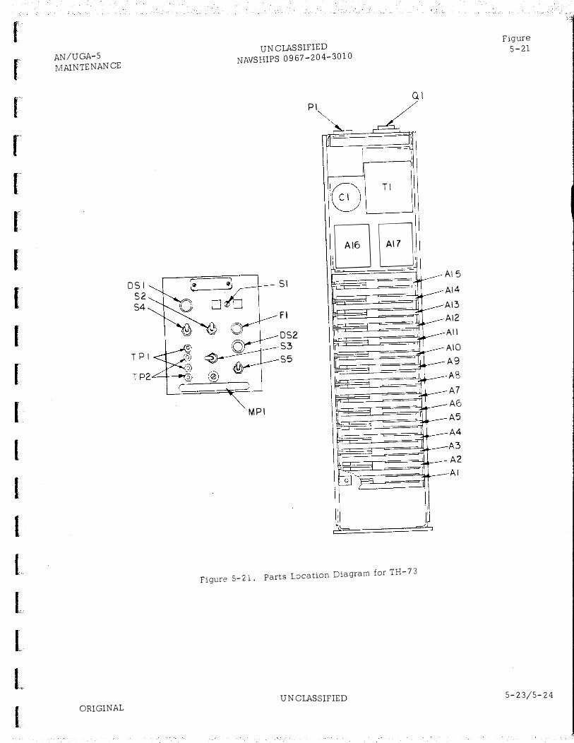
r
r
r
r
(
f
f
(
I
(
I
l
I
(
(
l.
l
L
t
AN/UGA-5 MAINTENANCE
ORIGINAL
OSI S2 S4
T PI
F� �
UNCLASSIFIED NAVSHIPS 0967-204-3010
------+--- S I
PI� � Ll
\1[ J I I 0[]''
\(;;\ Tl
0
BEJI7 1
: d I
I 1 - r
�
OIJJO
A\5
A\4
A\3 A\2
MPI
fl
DS2 S3 S5
� I I
Ill
1 rr '!
All
AIO A9 AS
A7 A6
.-- A5 'l
I A4
�� .A3
� A2
� ';:=:j AI
I I
�
{_
Figure 5-21 . Parts L::Jca tion Diagram for TH -7 3
UNCLASSIFIED
Figure
5-21
5- 2 3/5-2 4


I
r
r
r
I
(
I
I
(
(
I
(
I
(
l
l
l
L
t
AN/UGA-5 PARTS LIST
6-1. INTRODUCTION.
UNCLASSIFIED NAVSHIPS 0967-204- 3010
SECTION 6
PARTS LIST
P aragraph
6-1
a. REFERENCE DESIGNATIONS. - A uniform identification method has been used to identify the
chassis unit, assemblies, and maintenance parts of the AN/UGA-5. This method adequately covers
the several degrees of subdivision of the equipment. Examples of this method are illustrated by the
following:
Example 1:
Chassis Unit
Idenfitication No.
1 R l
Class of �art Part No.
within class
Read as: First (1) resistor (R) of chassis unit (1).
Example 2:
Chassis Unit
Identification No.
l.lil.
Assembly
Designation
Assembly
No.
Read as: First (1) assembly (A) of chassis unit (1).
Example 3:
Chassis Unit
Identification No.
1.. Al R1
Assembly
Designation
and No.
Class and
No. of Part
Read as: First (1) resistor (R) of first (1) assembly
(A) of chassis unit (1).
b. REF DESIG PREFIX. - Partial reference designations are used on the equipment and illustra
tions. The partial reference designations consist of the class letter(s) and the identifying item num
ber. The complete reference designations may be obtained by placing the proper prefix before the par
tial reference designations. Prefixes are provided on illustrations following the .notation "REF DESIG
PREFIX. II
6-2. LIST OF ASSEMBLIES.
Table 6-1 identifies the assemblies contained in the equipment. For the printed-circuit subassem
blies, the table lists identification numbers (and colloquial names) which will enable identification of these assemblies if the assembly reference designations on the extractor handle tabs become obliterated.
ORIGINAL UNCLASSIFIED 6-1

Paragraph
6- 2 UNCLASSIFIED
NAVSHIP S 0967-204-3010
AN/UGA-5 P ARTS LIST
The last column of the table provides an index to facilitate location of the maintenance parts list for
each assembly.
TABLE 6-l. LIST OF ASSEMBLIES
ASSY QTY PRINTED-CIRCUIT PARTS REF PER IDENTIFICATION LIST
DESIG EQUIP NUMBER COLLOQUIAL NAME PAGE
1 1 - Cabinet, Electrical Equipment 6-3
1A1 1 - Repeater, Telegraph TH-73/UGA-5 6-3
1A1 1 - Chassis Unit (Chassis, Electrical 6-3 Equipment)
1A1A1 1 D80060010-0l Oscillator (76.8kc and 93.237kc) 6-4
1A1A2 1 D80060010-02 Oscillator (125. 217kc and 152. 016kc) 6-5
1A1A3 1 D80060020 External Timing Interface 6-5
1A1A4 1 D80060030 Time Base Generator 6-7
1A1A5 1 D80060040-01 Add-Subtract Logic 6-8
1A1A6 1 D80060050-0l Signal Bit Timer 6-8
lAlA7 1 D80060040-02 Window Generator and Signal Bit Timer 6-9
1A1A8 1 D80060050-02 Start-Stop Character Control 6-10
1AlA9 1 D80060060 Mark-Hold (P/0 Automatic Disconnect Logic) 6-ll
1A1Al0 1 D80060040-03 Mode Decision and Data Regenerator 6-12
1A1All 1 D80060070 Sync Sample Detector 6-13
1A1A12 1 D80060050-03 Automatic Disconnect Counter Input Gates 6-14
1A1A13 1 D80060040-04 Automatic Disconnect Counter 6-15
1A1A14 1 D80060080 Automatic Disconnect Data Input and 6-16
Counter Output Gates
1A1A15 1 D80060090 Power Supply 6-17
1AlA16 1 A46000002 Input Interface
1AlA17 1 * A46000003 Output Interface
1AlA18 1 D80060100 Harness Board 6-18
*Replaced by A46000003-001 (both types are interchangeable)
6-2 UNCLASSIFIED ORIGINAL
1
,
1
1
l
]
"l
]
]
]
]
]
]
]
J
J
J
J
l

I
r
r
r
I
(
r
(
(
I
l
I
I,
I
I
1
L
L
t
AN/UGA-5 P ARTS LIST
ASSY REF
DESIG
lA2
1A3
1A4
l AS
1W1
QTY PER
EQUIP
l
1
l
l
l
UNCLASSIFIED NAVSHIPS 0967-204-3010
TABLE 6-1. LIST OF ASSEMBLIES (Cont'd)
PRINTED-CIRCUIT IDENTIFICATION
NUMBER COLLOQUIAL NAME
- Same As l Al
- Same As 1Al
- Same As 1A1
- Adapter Card
- Cable Assembly
6-3. MAINTENANCE PARTS LIST.
Table 6-1
PARTS LIST
PAGE
6-3
6-3
6-3
6-18
I 6-18 1
Table 6-2 lists the cabinet, chassis unit, and all assemblies, and their respective maintenance parts, except for input and output interfaces (subassembly Al6 and Al7), which are sealed plug-in units. Maintenance parts, in each case, are listed alphanumerically following the chassis unit identification and the assembly designation (where applicable). The table provides the following information: (l ) the complete reference designation of each maintenance part, (2) reference to explanatory notes, as required, (3) name and description of maintenance part, (4) listing of illustration
which pictorially locates the part.
TABLE 6-2. REPEATER GROUP, TELEGRAPH AN/UGA-5 MAINTENANCE P ARTS LIST
ASSEMBLY l, CABINET
REF
DESIG NOTES NAME AND DESCRIPTION
1 CABINET, ELECTRICAL EQUIPMENT: consists of front panel and parts mounted thereon; D9006000l (96238)
lCl-lC28 CAPACITOR: MIL type CK62BX102K
lFLl FILTER, BP: A43020007 (96238)
lTBl-lTB4 TERMINAL BOARD: 20109 (75382)
l XAl-lXA4 CONNECTOR, RECEPTACLE, ELECTRICAL: female, 13 con-tact, 10 amps; A48030058-8 (96238)
ASSEMBLY 1A1, CHASSIS UNIT
REF DESIG NOTES NAME AND DESCRIPTION
lAl CHASSIS, ELECTRICAL EQUIPMENT: used to mount the be-low listed items; D90060002 (96238)
lAlCl CAPACITOR: MIL type CE 51C501G 1A l C2 CAPACITOR: MIL type CE13C221G lAlDSl IAMP, INCANDESCENT: 349 (08806) 1AlDS2 IAMP: MIL type MS25252NE2D lAlFl FUSE, CARTRIDGE: visual indicating, 3/4 amp; GBA3-4
(71400)
ORIGINAL UNCLASSIFIED
FIGURE NUMBER
5-21
5-19
5-19
5-19
5- 1 9
FIGURE NUMBER
5-21
5-21 5-20 5-21 5-21
5-21
6-3

Table 6-2
REF DESIG
lAlJl
lAlMPl lAlQl lAlSl 1AlS2-1AlS5 lAl TPl lAl TP2-1AlTP4 lAlTl 1AlXA16 1AlXA17 lAlXCl lAlXDSl lAlXDS2 lAlXFl
UNCLASSIFIED N AVSHIP 0 967-204-3010
TABLE 6-2. REPEATER GROUP, TELEGRAPH AN/UGA-5 MAINTENANCE PARTS LIST (Cont'd)
NOTES NAME AND DESCRIPTION
CONNECTOR, RECEPTACLE, ELECTRICAL: male, 13 contacts; A48030057 -8 (96238) HANDLE, BOW: Bl013l-2 (96238) TRANSISTOR: MIL type 2N297A SWITCH, ROTARY: A4602010l (96238) SWITCH: MIL type MS25100-23 JACK, TIP: MIL type MS16108-1A
JACK, TIP: MIL type MS16108-3A TRANSFORMER, POWER: step-down; A43000070 (96238) SOCKET, ELECTRON TUBE: 78RSllT (02660) SOCKET, ELECTRON TUBE: TSlOlPOl (81349) SAME AS 1AlXAl7 LIGHT: MIL type LH73LC12CN LIGHT: MIL type LH74LC13CN FUSEHOLDER: HLD (71400)
ASSEMBLY lAlAl, OSCILLATOR 76. 8KC and 93. 237KC
REF DESIG NOTES NAME AND DESCRIPTION
lAlAl OSCILLATOR: ?G. 8kc and 93. 237kc, consists of a printed-circuit board which mounts and supplies the circuitry for the below listed items; D80060010-0l (96238)
lAlAlCl CAPACITOR, VARIABLE, GlASS: 0. 8-30pf, 200v; VC43GWY (73899)
1AlAlC2 Not used 1A1A1C3 CAPACITOR: MIL type CM06D202J03 1AlA1C4 CAPACITOR: MIL type CM06D681J03
1A1A1C5 CAPACITOR: MIL type CP09A1KB104K3 1A1A1C6 CAPACITOR: MIL type CM05D200J03 1AlA1C 7 Same as 1A1A1C3 1A1A1C8 Same as 1A1A1C4 1A1A1C9 Same as 1A1A1C5 1A1A1Q1 TRANSISTOR: MIL type 2N1225 1A1A1Q2 TRANSISTOR: MIL type 2N 404 1A1A1Q3 Same as 1A1A1Q1 1A1Al Q4 Same as 1A1AlQ2 1A1A1R1 RESISTOR: MIL type RC20GF683J lA1AlR2 RESISTOR: MIL type RC20GF752J lA1AlR3 RESISTOR: MIL type RC20GF472J 1AlAlR4 RESISTOR: MIL type RC20GF200J 1AlA1R5 RESISTOR: MIL type RC20GF132J 1AlA1R6 RESISTOR: MIL type RC20GFl03J 1A1A1R7 Same as 1A1A1Rl 1A1A1R8 Same as 1AlA1R2 lAlA1R9 Same as 1A1A1R3 lAlA1RlO Same as lA1A1R4 lA1A1R1l Same as 1AlA1R5 1A1A1R12 Same as 1A1A1R6
6-4 UNCLASSIFIED
AN/UGA-5 P ARTS LIST
FIGURE NUMBER
5-21 5-21 5-21 5-21 5-21 5-21
5-21 5-21 5-21 5-21 5-21 5-21 5-21 5-21
FIGURE NUMBER
5-l
5-l
5-1 5-1 5-1 5-1
5-1 5-1
5-1 5-l 5-l 5-l 5-l 5-1
ORIGINAL
I
,
1
1
�1
1
1
]
]
]
]
J
]
J
l
l
J
J
)

r
r
f
r
(
f
r
I
I
(
I
I
[
(
I
[
l
L
L
AN/UG A-5 PARTS LIST
REF DESIG
lAlAlYl 1AlAlY2
UNCLASSIFIED N AVSHIPS 0967-204-3010
TABLE 6-2. REPEATER GROUP, TELEGRAPH AN/UGA-5 MAINTENANCE PARTS LIST (C o nt'd)
NOTES NAME AND DESCRIPTION
CRYSTAL: MIL type CR37AU125-217KC CRYSTAL: MIL type CR37AU152-016KC
ASSEMBLY 1AlA2, OSCILLATOR 125.2l7KC and l52.0l6KC
REF DESIG NOTES NAME AND DESCRIPTION
lAlA2 OSCILLATOR: 125. 217kc and 152. 016kc, consists of a printed-circuit board which mo unts and supplie s the cir-cuitry for the below listed items; D80060010-02 (96238)
1AlA2Cl CAPACITOR, VARIABLE, GLASS: 0. 8-30pf, 200v; VC43GWY (73899)
1AlA2C2 N ot used 1AlA2C3 CAPACITOR: MIL type CM06D202J03 lAlA2C4 CAPACITOR: MIL type CM-5D331J03 lAlA2C5 CAPACITOR: MIL type CP09AlKB104K3 1AlA2C6 CAPACITOR: MIL type CM05D200J03 1AlA2C7 Same as 1AlA2C3 lAlA2C8 Same as lAlA2C4 lAlA2C9 Same as 1AlA2C5 1AlA2Ql TRANSISTOR: MIL type 2Nl225 lAlA2Q2 TRANSISTOR: MIL type 2N404 1AlA2Q3 Same as 1AlA2Ql 1AlA2Q4 Same as lAlA2Q2 1AlA2Rl RESISTOR: MIL type RC20GF683J 1AlA2R2 RESISTOR: MIL type RC20GF752J lAlA2R3 RESISTOR: MIL type RC20GF472J 1AlA2R4 RESISTOR: MIL type RC20GF200J 1AlA2R5 RESISTOR: MIL type RC20GF132J 1AlA2R6 RESISTOR: MIL type RC20GF1 03J 1AlA2R7 Same as 1AlA2Rl 1AlA2R8 Same as 1AlA2R2 lAlA2R9 Same as lAlA2R3 lAlA2RlO Same as lAlA2R4 1AlA2Rll Same as lAlA2R5 1AlA2Rl2 Same as 1AlA2R6 1AlA2Yl CRYSTAL: MIL type CR37AU125, 217KC lAlA2Y2 CRYSTAL: MIL type CR3 7AU152. Ol6KC
ASSEMBLY lAlA3, EXTERNAL TIMING INTERFACE
REF DESIG NOTES
1AlA3
1AlA3CRl-1AlA3CR7 lAlA3Cl 1AlA3C2, 1AlA3C3
ORIGINAL
NAME AND DESCRIPTION
EXTERNAL TIMING INTERFACE: co nsists o f a pri nted circuit board which mo unts and supplies the circuitry for the be-
low listed ite ms; D80060020 (96238)
SEMICONDUCTOR DEVICE: MIL type lN270 CAPACITOR:
CAPACITOR:
MIL type CS13AF010K
MIL type CM-6D681J03 -----� -- --
UNCLASSIFIED
----- �---------�-----
Table 6-2
FIGURE NUMBER
5-l 5-l
FIGURE NUMBER
5-l
5-l
5-l 5-l 5-l 5-l
5-l 5-l
5-l 5-l 5-l 5-l 5-l 5-l
5-l 5-l
FIGURE NUMBER
i '
5-3
5-3 5-3
5-3 ------
6-5

Table 6-2
REF DESIG
lAlA3C4 lAlA3C5, lAlA3C6 lAlA3Ql-lAlA3Q3 lAlA3Q4, lAlA3Q5 lAlA3Q6-lAlA3Q8 lAlA3Q9, lAlA3QlO lAlA3Rl lAlA3R2, lAlA3R3 lAlA3R4, lAlA3R5 lAlA3R6, lAlA3R7 lAlA3R8 1AlA3R9 lAlA3RlO 1AlA3Rll 1AlA3Rl2, 1AlA3Rl3 lAlA3Rl4, 1AlA3Rl5 1AlA3Rl6, lAlA3Rl7 lAlA3Rl8, lAlA3Rl9 lAlA3R20, 1AlA3R2l lAlA3R22, lAlA3R23 lAlA3R24 lAlA3R25 1AlA3R26 lAlA3R27 lAlA3R28, lAlA3R29 1AlA3R30, lAlA3R3l lAlA3R32
6-6
UNCLASSIFIED NAVSHIPS 0967-204-3010
TABLE 6-2. REPEATER GROUP, TELEGRAPH AN/UGA-5 MAINTENANCE PARTS LIST (Cont'd)
NOTES NAME AND DESCRIPTION
Same as lAlA3Cl
Same as lAlA3C2
TRANSISTOR: MIL type 2N404
TRANSISTOR: MIL type 2Nl306
Same as lAlA3Ql
Same as lAlA3Q4 RESISTOR: MIL type RC20GF682J
RESISTOR: MIL type RC20GF202J
RESISTOR: MIL type RCZOGFlOlJ
RESISTOR: MIL type RC20GF102J Same as lAlA3Rl RESISTOR: MIL type RC20GF183J RESISTOR: MIL type RC20GF391J Same as 1AlA3R9
RESISTOR: MIL type RC20GF223J
RESISTOR: MIL type RC20GF332J
Same as 1AlA3Rl
Same as 1AlA3R2
Same as 1AlA3R4
Same as 1AlA3R6 Same as 1AlA3Rl Same as lAlA3R9 Same as 1AlA3RlO Same as 1AlA3R9
Same as 1AlA3Rl2
Same as lAlA3Rl4 Same as lAlA3Rl
UNCLASSIFIED
AN/UG A-5 PARTS LIST
FIGURE NUMBER
I
5-3
5-3
5-3
5-3
5-3
5-3
5-3 5-3
5-3
5-3
ORIG INAL
1
,
,
l
l
�1
�1
'1
]
]
]
]
]
J
,J
J
J
J
J

( r I r· r r I (" ( [ ( [ l 1 l l L t t
AN/UGA-5 PARTS LIST
UNCLASSIFIED NAVSHIPS 0967-204-3010
TA BLE 6-2. REPEATER GROUP, TELEGRAPH AN/UGA-5 MAINTENANCE PARTS LIST (Cont'd)
ASSEMBLY lAlA4, TIME BASE GENERATOR
REF DESIG
lAlA4
lAlA4CRl-lAlA4CRl2 lAlA4CRl3, lAlA4CRl4 lAlA4Cl, lAlA4C2 1AlA4C3-lAlA4C 14 1AlA4Ql-1AlA4Q9 lAlA4Rl lAlA4R2, lAlA4R3 1AlA4R4 1AlA4R5, lAlA4R6 1AlA4R7, 1AlA4R8 1AlA4R9 1AlA4Rl0 lAlA4Rll 1AlA4Rl2 1AlA4Rl3 lAlA4Rl4 lAlA4Rl5, lAlA4Rl6 lAlA4Rl7, lAlA4Rl8 lAlA4Rl9, 1AlA4R20 lAlA4R2l, lAlA4R22 lAlA4R23, lAlA4R24 lAlA4R25, lAlA4R26 lAlA4R27, lAlA4R28 lAlA4R29, lAlJIAR30 lAlA4R31, lAlA4R32 lAlA4R33, lAlA4R34 1AlA4R35, lAlA4R36
ORIGINAL
I NOTES NAME AND DESCRIPTION
TIME BASE GENERATOR: consists of a printed-circuit b oard which mounts and supplies the circuitry for the b elow listed items; D80060030 (93238)
SEMICONDUCTOR DEVICE: MIL type 1N270
SEMICONDUCTOR DEVICE: MIL type 1N914
CAPACITOR: MIL type CK62AX822K
CAPACITOR: MIL type CM05Dl51J03
TRANSISTOR: MIL type 2N404 RESISTOR: MIL type RC20GF223J
RESISTOR: MIL type RC2CGF222J Same as 1AlA4Rl
Same as 1AlA4R2
RESISTOR: MIL type RC20GF682J Not used Not used Same as 1AlA4R2 Same as 1AlA4Rl RESISTOR: MIL type RC20GF332J Same as 1AlA4Rl3
Same as 1AlA4Rl
RESISTOR: MIL type RC20GF823J
RESISTOR: MIL type RC 2 OGF 15 3J
Same as lAlA4Rl3
Same as 1AlA4Rl
Same as 1AlA4Rl7
Same as 1AlA4Rl9
Same as 1AlA4Rl3
Same as 1AlA4Rl
Same as lAlA4Rl7
Same as lAlA4R19
UNCLASSIFIED
Table 6-2
FIGURE NUMBER
5-5
5-5
5-5
5-5
5-5
5-5 5-5
5-5
5-5
5-5
5-5
5-5
6-7

Table 6-2
UNCLASSIFIED NAVSHIP S 0967-204-3010
TABLE 6-2. REPEATER GROQP, TELEGRAPH AN/UGA-5 MAINTENANCE PARTS LIST (Cont'd)
ASSEMBLY 1AlA5, ADD-SUBTRACT LOGIC
REF DESIG
1AlA5
lAlA5CRllAlA5CRl2 1AlA5C llAlA5Cl6 lAlA5QllAlA5Q8 lAlA5Rl lAlA5R2 lAlA5R3 lAlA5R4, lAlA5R5 lAlA5R6 1AlA5R7 lAlA5R8 1AlA5R9 lAlA5RlO lAlASRll 1AlA5Rl2, lAlA5Rl3 1AlA5Rl4 lAlA5Rl5 lAlA5Rl6, lAlA5Rl7 lAlA5Rl8 lAlA5Rl9 lAlA5R20, lAlA5R2l lAlA5R22 lAlA5R23 lAlA5R24, lAlA5R25 lAlA5R26 lAlA5R27 lAlA5R28, lAlA5R29 lAlA5R30 lAlA5R3l lAlA5R32
NOTES NAME AND DESCRIPTION
ADD-SUBTRACT LOGIC: consists of a printed-circuit b oard wh ich m o unts and supplies the circuitry for the below listed items; D80060040-0l (96238)
SEMICONDUCTOR DEVICE: MIL type lN270
CAPACITOR: MIL type CM-5Dl51J03
TRANSISTOR: MIL type 2N 404 RESISTOR: MIL type RC20GF332J RESISTOR: MIL type RC20GF153J RESISTOR: MIL type RC20GF223J
RESISTOR: MIL type RC20GF823J Same as 1AlA5R3 Same as lAlA5Rl Same as 1AlA5R2 Same as lA1A5Rl Same as lAlA5R2 Same as 1AlA5R3
Same as 1AlA5R4 Same as 1A1A5R3 Same as lAlASRl
Same as 1AlA5R2 Same as lAlA5Rl Same as lAlA5R3
Same as lAlA5R4 Same as lAlA5R3 Same as lAlA5Rl
Same as lAlA5R2 Same as lAlA5Rl Same as lAlA5R3
Same as lAlA5R4 Same as lAlA5R3 Same as lAlA5Rl Same as lAlA5R2
ASSEMBLY 1AlA6, SIGNAL BIT TIMER
REF DESIG NOTES NAME AND DESCRIPTION
lAlA6 SIGNAL BIT TIMER: consists of a pr inted-circuit b oard wh ich m o unts and sup plies the circuitry for the below listed items; D80060050-0l (96238)
1AlA6CRl-lAlA6CRl7 SEMICONDUCTOR DEVICE: MIL type lN270
----- --·---- ----
6-8 UNCLASSIFIED
AN/UGA-5
PARTS LIST
FIGURE NUMBER
5-7
5-7
5-7
5-8 5-9 5-10 5-ll
5-12
FIGURE NUMBER
5-9
5-9
ORIGINAL
'1
1
1
1
1
''1
']
l
1
]
]
-]'_ --
•1-. ;.;
J
l
J
l
J
J

r
r
r
r
(
(
(
(
(
(
f
I
[
l
[
[
L
L
L
AN/UGA-5 PARTS LIST
REF DESIG
1AlA6Cl, lAlA6C2 1AlA6C3 1AlA6C4-lAlA6Cl5 1AlA6Ql-lAlA6Q8 1AlA6Rl lAlA6R2 lAlA6R3 lAlA6R4 lAlA6R5 lAlA6R6 lAlA6R7 lAlA6R8 lAlA6R9 lAlA6RlO lAlA6Rll lAlA6Rl2 1AlA6Rl3 lAlA6Rl4 1AlA6Rl5, 1AlA6Rl6 1AlA6Rl 7
lAlA6Rl8 1AlA6Rl9, lAlA6R20 lAlA6R21
1AlA6R22 1AlA6R23, 1AlA6R24 1AlA6R25 lAlA6R26 1AlA6R27, lAlA6R28 lAlA6R29 1AlA6R30 1AlA6R3l
UN CLASSIFIED N AVSHIPS 0967-204-3010
TABLE 6-2. REPEATER GROUP, TELEGRAPH AN/UGA-5 MAINTENANCE PARTS LIST (Cont'd)
NOTES NAME AND DESCRIPTION
Not used CAPACITOR: MIL type CM06Dl02J03
Same as 1AlA6Cl
TRANSISTOR: MIL type 2N404 RESISTOR: MIL type RC20GF682J RESISTOR: MIL type RC20GF103J RESISTOR: MIL type RC20GF683J RESISTOR: MIL type RC20GF332J Same as 1AlA6Rl Same as lAlA6R2 Same as 1AlA6R3 RESISTOR: MIL type RC20GF153J Same as lAlA6R4 RESISTOR: MIL type RC20GF223J RESISTOR: MIL type RC20GF823J Same as 1AlA6Rll Same as 1AlA6RlO Same as 1AlA6R4
Same as 1AlA6R8 Same as 1AlA6R4 Same as lAlA6RlO
Same as lAlA6Rll Same as 1AlA6Rl 0 Same as 1AlA6R4
Same as 1AlA6R8 Same as 1AlA6R4 Same as lA lA 6Rl 0
Same as 1AlA6Rll Same as 1AlA6RlO Same as lAlA6R4 Same as 1AlA6R8
ASSEMBLY 1AlA7, WINDOW GENERATOR AND SIGNAL BIT TIMER
REF DESIG NOTES NAME AND DESCRIPTION
lAlA7 WINDOW GENERATOR AND SIGNAL BIT TIMER: consists of a printed-circuit board which mounts and supplies the circuitry for the below listed items; D80060040-02 (96238)
1AlA7CRl-
1AlA7CR12 SEMICONDUCTOR DEVICE: MIL type 1N270
------ -----------CRIG INAL UNCLASSIFIED
Table 6-2
FIGURE ! NUMBER
5-9 I
5-9 5-9 5-9 5-9 5-9
5-9
5-9 5-9
FIGURE NUMBER
5-7
5-7
6-9

Table 6-2
REF
DESIG
lAlA7Cl-lAlA7Cl6 lAlA7Ql-lAlA7Q8 lAlA7Rl-lAlA7R3 lAlA7R4, lAlA7R5 1AlA7R6 lAlA7R7 lAlA7R8 lAlA7R9 lAlA7RlO lAlA7Rll lAlA7Rl2, lAlA7Rl3 lAlA7Rl4 lAlA7Rl5 lAlA7Rl6, lAlA7Rl7 lAlA7Rl8 lAlA7Rl9 lAlA7R20, lAlA7R2l lAlA7R22 lAlA7R23 lAlA7R24, lAlA7R25 lAlA7R26 lAlA7R27 lAlA7R28 lAlA7R29 1AlA7R30 lAlA7R3l 1AlA7R32
UN CLASSIFIED NAVSHIPS 0967-204-3010
TABLE 6-2. REPEATER GROUP, TELEGRAPH AN/UGA-5 MAINTENANCE PARTS LIST (Cont'd)
NOTES NAME AND DESCRIPTION
CAPACITOR: MIL type CM05Dl5lJ03
TRANSISTOR: MIL type 2N404
RESISTOR: MIL type RC20GF332J
RESISTOR: MIL type RC20GF823J Same as lAlA7R3 Same as lAlA7Rl Same as lAlA7R2 Same as lAlA7Rl Same as lAlA7R2 Same as lAlA7R3
Same as lAlA7R4 Same as lAlA7R3 Same as lAlA 7Rl
Same as lAlA7R2 Same as lAlA7Rl Same as lAlA7R3
Same as lAlA7R4 Same as lAlA7R3 Same as lAlA7RJ
Same as 1AlA7R2 Same as lAlA7Rl Same as 1AlA7R3 Same as lAlA7R4 Same as lAlA7R4 Same as lAlA7R3 Same as lAlA7Rl Same as lAlA7R2
------
ASSEMBLY lAlA8, START-STOP CHARACTER CONTROL
REF
DESIG NOTES NAME AND DESCRIPTION
lAlAS START-STOP CHARACTER CONTROL: Consists of a pr inted-circuit board which mo unts and supplies the circuitry for th� below listed items; D80060050-02 (96238)
lAlASCRl - SEMICONDUCTOR DEVICE: MIL type 1N270 lAlA8CRl7
lAlASCl, Not used 1AlA8C2 lAlA8C 3 CAPACITOR: MIL type CM06Dl02J03 1AlA8C4- Same as lAlASCl
6-10 UNCLASSIFIED
AN/UGA-5 PARTS LIST
FIGURE NUMBER
5-7
5-7
5-7
5-7
FIGURE
NUMBER
5-9 5- 9
5-9
ORIGINAL
1
1
1
1
1
�1
1
]
]
]
'] �'l
J
J
J
l
J
J '
J
J

r
r
r
r
I
(
f
(
(
(
I
I
l
l
I
l
l
L
t
AN/UGA-5 PARTS LIST
REF DESIG
lAlA8Cl5 1AlA8Ql -1AlA8Q8 1AlA8Rl 1AlA8R2 lAlA8R3 lAlA8R4 lAlA8R5 1AlA8R6 lAlA8R7 1AlA8R8 lAlA8R9 lAlABRlO 1AlA8Rll, 1AlA8Rl2 lAlA8Rl3 1AlA8Rl4 1AlA8Rl5, 1AlA8Rl6 1AlA8Rl7 1AlA8Rl8 lAlA8Rl9, lAlA8R20 lAlA8R21 1AlA8R22 lAlA8R23, 1AlA8R24 1AlA8R25 lAlA8R26 lAlA8R27, 1AlA8R28 lAlA8R29 lAlA8R30 lAlA8R3l
UNCLASSIFIED NAVSHIPS 0967-204-3010
TABLE 6-2. REPEATER GROUP, TELEGRA PH AN/UGA-5 MAINTENANCE PARTS LIST (Cont'd )
NOTES NAME AND DESCRIPTION
TRANSISTOR: MIL type 2N 404
RESISTOR: MIL type RC20GF682J RESISTOR: MIL type RC20GF1 03J RESISTOR: MIL type RC20GF683J RESISTOR: MIL type RC20GF332J Same as 1AlA8Rl Same as 1AlA8R2 Same as 1AlA8R3 RESISTOR: MIL type RC20GF153J Same as lAlA8R4 RESISTOR: MIL type RC20GF223J RESISTOR: MIL type RC20GF823J
Same as lAlA8Rl 0 Same as lAlA8R4 Same as lAlA8R8
Same as lAlA8R4 Same as lAlA8Rl 0 Same as lAlA8Rll
Same as lAlA8Rl 0 Same as lAlA8R4 Same as lAlA8R8
Same as lAlA8R4 Same as lAlA8Rl 0 Same as lAlABRll
Same as lAlA8Rl 0 Same as lAlA8R4 Same as 1AlA8R8
ASSEMBLY lAlA9, MARK-HOLD (P/0 AUTOMATI C DISCONNE CT LOGIC)
REF DESIG NOTES NAME AND DESCRIPTION
lAlA9 MARK-HOLD (P/0 AU TOMATIC DISCONNECT LOGIC): Con-sists of a printed-circuit board which mo unts and supplies the circuitry fo r the below listed items; D80060060 (96238)
1AlA9CRl - SEMICONDUCTOR DEVICE: MIL type lN270
1AlA9CRll lAlA9Cl, CAPACITOR: MIL type CM06Dl02J03
lAlA9C2 lAlA9C3 CAPACITOR: MIL type CM05Dl5lJ03
lAlA9C4 Same as lAlA9Cl
1AlA9Ql - TRANSISTOR: MIL type 2N 404
lAlA9Q9 lAlA9Rl, RESISTOR: MIL type RC20GF223J
ORIGINAL UNCLASSIFIED
Table 6 -2
FIGURE NUMBER
5-9
5-9 5-9 5-9 5-9
5-9
5-9 5-9
----
FIGURE NU MBER
5-ll
5-ll
5-ll
5-11
5-ll
5-11
6-11

Table
6 -2
REF DESIG
lAlA9R2 lAlA9R3 lAlA9R4 lAlA9R5. lAlA9R6 lAlA9R7 lAlA9R8 lAlA9R9 lAlA9Rl0 lAlA9Rll -lAlA9Rl3 lAlA9Rl4 lAlA9Rl5 lAlA9Rl6 lAlA9Rl7 lAlA9Rl8 lAlA9R�9 lAlA9R20 lAlA9R2l lAlA9R22 lAlA9R23 lAlA9R24 lAlA9R25 lAlA9R26 lAlA9R27 lAlA9R28 lAlA9RL 9 I
lAlA9R30 lAlA9R3l lAlA9R32 lAlA9R33 lAlA9R34 lAlA9R35
UNCLASSIFIED
NAVSHIPS 0967-204-3010
TABLE 6-2. REPEATER GROUP, TELEGRAPH AN/UGA-5 MAINTENANCE PARTS LIST (Co nt'd)
NOTES NAME AND DESCRIPTION
RESISTOR: MIL type RC20GF683J RESISTOR: MIL type RC20GF472J Same as lAlA9Rl RESISTOR: MIL type RC20GF823J Same as lAlA9R4 Same as lAlA9Rl RESISTOR: MIL type RC20GFl 02J Same as lAlA9R4 Same as lAlA9Rl
Same as lAlA9R3 Same as lAlA9R4 Same as lAlA9Rl Same as lAlA9R6 Same as lAlA9R4 Same as lAlA9Rl Same as lAlA9R9 Same as lAlA9R4 Same as lAlA9R3 RESISTOR: MIL type RC20GFl53J Same as lAlA9R4 RESISTOR: MIL type RC20GF333J Same as lAlA9Rl Same as lAlA9R4 Same as lAlA9R6 RESISTOR: MIL type RC20GF103J
RESISTOR: MIL type RC20GF682J Same as lAlA9R29 Same as lAlA9R3 Same as lAlA9R29 RESISTOR: MIL type RC20GFl2lJ
�--- '-------
ASSEMBLY lAlAl 01 MODE DECISION AND DATA REGENERATOR
REF DESIG NOTES
lAlAlO
lAlAl OCRl -lAlAl OCR12
lAlAlOCl -lAlAl0Cl6 lAlAlOQl -lldAl OQB
lAlAliJRl lAlAl ORZ lAlAlOR3 lAlAlOR41 lAlAlORS
6-12
NAME AND DESCRIPTION
MODE DECISION AND DATA REGENERATOR: Consists of a printed- circuit b oard which mo unts and supplies the cir-cuitry fo r the b elow listed items; D8006004-03 (96238)
SEMICONDUCTOR DEVICE: MIL type lN270
CAPACITOR: MIL type CM05Dl51J03
TRANSISTOR: MIL type 2N404
RESISTOR: MIL type RC20GF332J RESISTOR: MIL type RC20GF l53J RESISTOR: MIL type RC20GF223J RESISTOR: MIL type RC20GF823J
--- -----UNCLASSIFIED
- � ---- ---
AN/TJGA-5
PAR'l'S LIST
FIGURE NUMBER
5-ll 5-ll
5-ll
5-ll
I
I
5-11
5-11
5-ll
5-ll
5-ll
FiGURE NUMBER
5-7 5-7
5-7
5-7
5-7 5-7 5-7 5-7
CRIGINAL
,
,
1
�1
1
]
'l
1
]
]
]
:]
]
]
,)
J
J
J
l

f
r
r
r
r
(
(
r
(
r
I
l
l
(
l
l
t
L
I
AN/UG A-5 PARTS LIST
REF
DESIG lAlAlOR6 lAlAlOR7 lAlAlOR8 1AlAlOR9 lAlAlORlO lAlAl ORll 1A1Al0Rl2, lA1Al0Rl3 1AlAlOR14 lA1AlOR15 1AlAlOR16, lAlA10Rl7 lAlA10Rl8 lA1AlOR19 1A1Al0R20, 1A1A10R21 1AlA10R22 lAlAl0R23 1AlA10R24, 1AlAlOR25 lAlAl0R26 lAlAlOR27 lAlAl OR28, 1A1Al0R29 lA1AlOR30 1AlA10R31 1A1AlOR32
UN CLASSIFIED NAVSHIPS 0967-204-3010
TABLE 6-2. REPEATER GROUP, TELEGRAPH AN/UGA-5 MAI NTENANCE PARTS LIST (Cont'd)
.. NOTES NAME AND DESCRIPTION
Same as lAlAl OR3 Same as lAlAl ORl Same as lAlAl OR2 Same as lAlAl ORl Same as lAlAl OR2 Same as lAlAl OR3 Same as lAlAl OR4
Same as 1AlAl OR3 Same as lAlAl OR1 Same as lAlAl OR2
Same as lAlAl ORl Same as lAlAl 0R3 . Same as 1AlA1 OR4
Same as 1A1A1 OR3 Same as lAlAl ORl Same as 1AlAlOR2
Same as lAlAl ORl Same as lAlAl OR3 Same as 1AlA1 0R4
Same as 1A1A1 0R3 Same as 1A1A1 OR1 Same as lAlAl OR2
ASSEMBLY 1AlA11 SYNC SAMPLE DETECTOR
REF DESIG NOTES
lAlAll
lAlAllCRl -lA1AllCR8 lAlAllCl 1A1Al1C2 -1AlAllC5 1AlA11C6 lAlAllQl -lAlAl109 lAlAllR1 lAlA1lR2 lAlAllR3 lAlA11R4
lA1AllR5 lAlA11R6
lA1AllR7
1A1Al1R8
ORIGINAL
NAME AND DESCRIPTION
SYNC SAMPLE DETECTOR: Co nsists of a printed-circuit board which mo unts and supplies the circuitry fo r the b elow listed items; D80060070 (96238) SEMICONDUCTOR DEVICE: MIL type lN270
CAPACITOR: MIL type CS13AF330K CAPACITOR: MIL type CM05Dl51J03
CAPACITOR: MIL type CS13AF4R7K TRANSISTOR: MIL type 2N 404
RESISTOR: MIL type RC20GF223J RESISTOR: MIL type RC20GF683J RESISTOR: MIL type RC20GF221J RESISTOR: MIL type RC20GF152J RESISTOR: MIL type RC20GF472J RESISTOR: MIL type RC20GF473J Same as 1AlA11R5 RESISTOR: MIL type RC20GF682J - - - -
UNCLASSIFIED
-·-�···-
Table 6-2
FIGURE N UMBER
FIGURE NUMBER
5-13 5-13
I 5-13 5-13
5-13 5-13
5-13 I
5-13 5-13 5-13 5-13 5-13
5-13
6-13

Table 6-2
REF DESIG
1AlAllR9 lA1AllR10 1AlAllR1l 1AlAllR12 lA1AllR13, 1A1A11R14
lA1A1lR15 1AlA11R16 1A1AllR17 1A1AllR18 1A1A11Rl9
1A1AllR20, lA1AllR21 lA1AllR22
1A1AllR23 lA1AllR24
lAlAllR25 lAlAllR26 , lAlAllR27
lAlAl1R28 lAlAllR29 lAlA1lR30 lA1AllR3l
1AlAllR32
lA1AllR33 lA1AllR3 4
1A1AllR35
1A1AllR 3 6 1A1AllR37
1A1A11R38,
lAlA11R39
UN CLASSIFIED NAVSHIPS 0967-204-3010
TABLE 6-2. REPEATER GROUP, TELEGRAPH AN/UGA-5 MAINTENANCE PARTS LIST (Cont'd)
NOTES
·- - ·
NAME AND DESCRIPTION
RESISTOR: MIL type RC20GFl 03J Same as lA1AllR2 Same as lA1AllR9 RESISTOR: MIL type RC20GF100J Same as 1A1A11R1
Same as lA1A11R2 Same as lA1AllR5 RESISTOR: MIL type RC20GF153J RESISTOR: MIL type RC20GF332J Same as 1A1A11R1 RESISTOR: MIL type RC20GF823J
Same as lA1AllR1 Same as 1A1Al1Rl8 Same as 1A1AllR17 Same as lA1AllR9 Same as lA1AllRl
Same as lAlAllR2 Same as 1AlAl1R5 Same as 1AlAllR8 Same as lAlAllR9 Same as lA1A11R2 Same as lA1A11R9 Same as 1A1A11R12 RESISTOR: MIL type RC20GF222J Same as 1AlAll R6 Same as 1A1A11 R3 5 Same as 1A1A11R1
�
ASSEMBLY lAlAl2, AUTOMATIC DISCONNECT COUNTER INPUT GATES
REF
DESIG NOTES NAME AND DESCRIPTION
1AlA12 AUTOMATIC DISCONNECT COUNTER INPUT GATES: Consists of a printed-circuit board which mounts and supplies the circuitry for the below listed items; D80060050-03 (96238)
1A1A12CR1- SEMICONDUCTOR DEVICE: MIL type 1N270 1A1A12CR17 lAlA12Cl, Not used lAlAl2C2
lA1Al2C3- CAPACITOR: MIL type CM06Dl 02J03 1A1Al2Cl5 lA1Al2Ql- TRANSISTOR: MIL type 2N404 1AlAl2Q8
1AlA12Rl RESISTOR: MIL type RC20GF682J 1A1A12R2 RESISTOR: MIL type RC20GF103J 1AlA12R3 RESISTOR: MIL type RC20GF683J
6-1 4 UNCLASSIFIED
.
AN/UGA-5
P ARTS LIST
FIGURE
NUMBER
5-13
5-13
5-13 5-13
5-13
5-13
FIGURE
NUMBER
5-9 5-9
5-9
5-9
5-9 5-9 5-9
ORIGINAL
'1
,
1
1
l
l
l
'")
]
]
]
�)
]
J
J
J
J
J
J

I
r
r
r
('
r
I
(
I
I�
I
I
l
[
l
(,
l
L
t
AN/UGA-S PARTS LIST
REF
DESIG
lAlAl2R4
lAlAl2R5
lAlAl2R6
lAlAl2R7 lAlAl2R8
lAlAl2R9
lAlAl2Rl 0
lAlAl2Rll,
lAlAl2Rl2
lAlAl2Rl3
lAlAl2Rl4
lAlAl2Rl5 I
lAlAl2Rl6
1A1Al2Rl7
lAlAl2Rl8
lAlAl2Rl9 I
lAlAl2R20
lAlAl2R2l
lAlAl2R22
lAlAl2R23 I
lAlAl2R24
lAlAl2R25
lAlAl2R26
lAlAl2R2 7 I
lAlAl2R2 8
lAlA12R29
lAlA12R30
lAlA12R3l
UN CLASSIFIED N AVSHIPS 0967-204-3010
TABLE 6-2. REPEATER GROUP, TELEGRAPH AN/UGA-5 MAINTENANCE PARTS LIST (Cont'd)
NOTES NAME AND DESCRIPTION
RESISTOR: MIL type RC20GF332J Same as lAlAl2Rl Same as lAlAl2R2 Same as lAlAl2R3 RESISTOR: MIL type RC20GF153J Same as lAlAl2R4 RESISTOR: MIL type RC20GF223J RESISTOR: MIL type RC20GF823J
Same as lAlAl2Rl 0 Same as lAlAl2R4
Same as lAlAl2R8
Same as lAlAl2R4
Same as lAlAl2Rl 0 Same as Rll
Same as RlO
Same as lAlAl2R4
Same as lAlAl2R8
Same as lAlAl2R4 Same as lAlAl2Rl 0 Same as lAlAl2Rll
Same as 1AlAl2Rl 0 Same as lA1Al2R4
Same as 1A1Al2R8 ��-------·-···---- -------------------- --
ASSEMBLY 1A1Al3, AUTOMATIC DISCONNECT COUNTER
REF
DESIG
1AlAl3
lAlAl3CRl
lA1Al3CRl2
lAlAl3Cl-
1AlAl3Cl 6
lAlAl3Ql
lA1Al3Q8
lAlAl3Rl
1AlA13R2
lAlAl3R3
lAlAl3R41
lAlA13R5
1AlAl3R6
lAlAl3R7
lAlAl3R8
ORIGINAL
NOTES NAME AND DESCRIPTION
AUTOMATIC DISCONNECT COUNTER: Consists of a printedcircuit board which mounts and s upplies the circuitry for the below listed items; D80060040-04 (96238)
SEMICONDUCTOR DEVICE: MIL type lN270
CAPACITOR: MIL type CM05Dl51J03
TRANSISTOR: MIL type 2N404
RESISTOR: MIL type RC20GF332J RESISTOR: MIL type RC20GF153J RESISTOR: MIL type RC20GF223J RESISTOR: MIL type RC20GF823J
Same as lAlAl3R3 Same as lAlA13Rl Same as 1AlAl3R2
UNCLASSIFIED
Table 6-2
F IGURE NUMBER
5-9
5-9
5-9 5-9
I
FIGURE NUMBER
5-7
5-7
5-7
5-7
5-7 5-7
5-7 5-7
6-15

Table
6-2
REF
DESIG
lA1Al3R9 lAlA13RlO lAlAl3Rll lAlAl3Rl21 lA1Al3Rl3 lA1Al3Rl4 1AlAl3Rl5 1AlA13Rl61 1AlA13Rl 7 1A1Al3Rl8 lAlAl3Rl9 lAlAl3R20 I
1A1Al3R21 1AlAl3R22 lAlAl3R23 lAlAl3R241 lAlAl3R25 1AlAl3R26 lAlAl3R27 lAlAl3R281 lAlAl3R29 lAlAl3R30 lAlAl3R31 lAlAl3R32
UNCLASSIFIED
NAVSHIPS 0967-204-3010
TABLE 6-2. REPEATER GROUP 1 TELEGRAPH AN/UGA-5 MAINTENANCE PARTS LIST (Cont'd)
NOTES NAME AND DESCRIPTION
Same as 1A1Al3Rl Same as lAlA13R2 Same as 1A1Al3R3 Same as lAlA13R4
Same as 1AlAl3R3 Same as 1AlAl3Rl Same as 1AlA13R2
Same as lAlA13Rl Same as lA1Al3R3 Same as 1A1Al3R4
Same as lAlAl3R3 Same as lAlAl3Rl Same as lA1Al3R2
Same as lAlA13Rl Same as lAlAl3R3 Same as lAlAl3R4
Same as lAlAl3R3 Same as lAlAl3Rl Sg.me as _18.JA13R2 . ___ - -·--·-·-·-·-
ASSEMBLY 1A1Al4 1 AUTOMATIC D ISCONNECT DATA INPUT AND COUNTER OUTPUT GATES
REF
DESIG
lAlAl4
1AlA14CRl-1AlAl4CRl5
1AlA14C', 1A1Al4C 2 1A1Al4C3-lA1Al4C5 1AlAl4C 6-
1AlAl4C 9 lAlAl4Ql-1A1Al4Q6 1AlA14R1 1A1Al4R2 1AlAl4R3 lAlAl4R4 1A1A14R5 lA1Al4R6 1AlA14R7 1A1Al4R8
6-16
NOTES NAME AND DESCRIPTION
AUTOMATIC D ISCONNECT DATA INPUT AND COUNTER OUTPUT GATES: Consists of a printed-circuit board which mounts and supplies the circuitry for the below listed items; D80060080 (96238) SEMICONDUCTOR DEVICE: MIL type 1N270
CAPACITOR: MIL type CM05D221J03
CAPACITOR: MIL type CM05D391J03
CAPACITOR: MIL type CM05Dl51J03
T RANSISTOR: MIL type 2N404
RESISTOR: MIL type RC20GF683J RESISTOR: MIL type RC20GF153J Same as 1A1A14R2 Same as 1A1A14R1 RESISTOR: MIL type RC20GF222J Same as 1A1A14R1 Same as 1A1A14R5 RESISTOR: MIL type RC20GF223J
UN CLASSIF IED
AN/UGA-5
PARTS LIST
F IGURE
NUMBER
F IGURE NUMBER
5-15
5-15
5-15
5-15
5-15
5-15
5-15 5-15
5-15
5-15
I
O RIGINAL
1
1
1
1.
l
l
]
cl
]
]
]
]
J
J
J
l
J
J
J
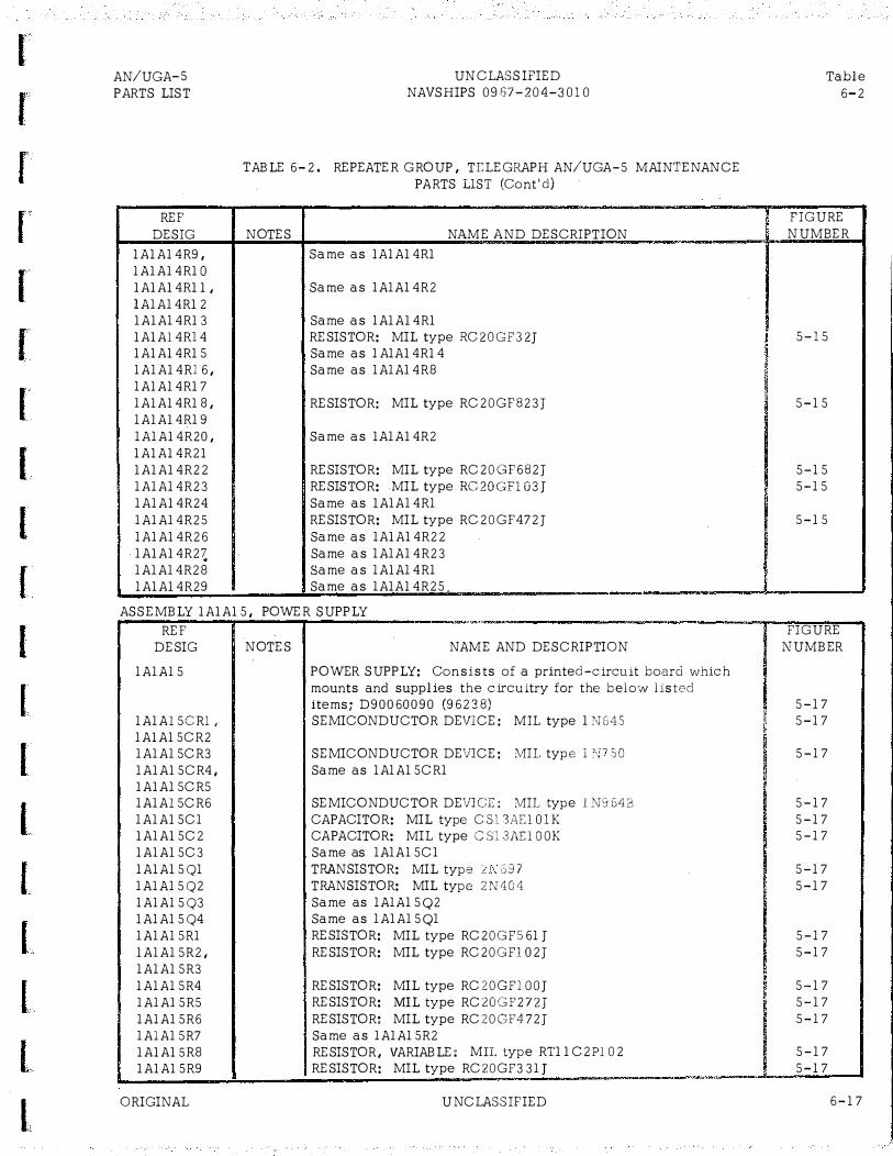
r
r
r
r
f
f
I
(
I
r
I
(
I
1
l
I
l
L
I;
AN/UGA-5 P ARTS L IST
REF DESIG
lAlAl4R9, lAlAl4RlO lAlAl4Rll, lA1A14Rl2 lAlA14Rl3 lAlAl4Rl4 lAlAl4Rl5 1A1Al4Rl6, 1AlAl4Rl7 1AlAl4Rl8, 1AlAl4R19 1A1Al4R20, lAlAl4R2l lAlAl4R22 1A1A14R23 1A1Al4R24 1A1A14R25 1A1A14R26 1AlAl4R2� 1A1A14R28 1A1Al4R29
UNCLASS IFIED NAVSHIPS 0967-204-3010
T ABLE 6-2. REPEATER GROUP, Tf.LEGRAPH AN/UGA-5 MAINTENANCE PARTS LIST (Cont'd)
NOTES NAME AND DESCRIPT ION
Same as lAlAl4Rl
Same as 1A1A14R2
Same as 1AlAl4Rl RESISTOR: MIL type RC20GF32J Same as 1 A1Al4Rl4 Same as 1A1A14R8
RESISTOR: MIL type RC20GF823J
Same as lA1Al4R2
RESISTOR: MIL type RC20GF682J RESISTOR: MIL type RC20GFl 03J
Same as lA1A14R1 RESISTOR: MIL type RC20GF472J Same as 1AlA14R22 Same as 1A1A14R23 Same as 1AlA14R1 Same as 1AlAl4R25_
ASSEMBLY lAlAl5, POWER SUPPLY
REF DESIG NOTES
1A1A15
1A1Al5CRl, 1AlA15CR2 1A1A15CR3 1A1A15CR4, lAlA15CR5 1A1Al5CR6 1A1Al5C1 lA1Al5C2 1A1Al5C3 1A1A15Q1 1A1A15Q2 1A1A15Q3 1A1A15Q4 1A1A15R1 lA1A15R2, 1A1A15R3 lA1A15R4 1A1A15R5 1A1A15R6 1AlA15R7 lAlAl5R8 lAlAl5R9
OR IGINAL
-
NAME AND DESCR IPTION
POWER SUPPLY: Consists of a printed-circuit board which mo unts and supplies the circuitry for the below listed items; D90060090 (96238) SEMICONDUCTOR DEVICE: MIL type 1 NG45
SEMICONDUCTOR DEVICE: MIL type 1 50
Same as 1A1A15CR1
SEMICONDUCTOR DEVICE: MIL type l N9 G4B
CAPACITOR: MIL type CS13Af:l01K
CAPACITOR: MIL type CSl3AElOOK
Same as 1A1A15C1 TRANSISTOR: MIL type 697
TRANSISTOR: MIL type 2N404
Same as 1A1A15Q2 Same as 1A1A15Q1 RESISTOR: MIL type RC20GF5 61 J
RESISTOR: MIL type RC20GF1 02J
RESISTOR: MIL type RC 20GFl OOJ
RESISTOR: MIL type RC20GF272J RESISTOR: MIL type RC20GF472J Same as 1A1A15R2 RESISTOR, VAR IABLE: MIL type RTllC2Pl02 RESISTOR: MIL type RC20GF3 31 J
U NCLASSIF IED
'
;
" �
� hl
�
I
Table
6-2
FIGURE NUMBER
5-15
5-15
5-15 5-15
5-15
I
FIGURE NUMBER
5-17 5-17
5-17
5-17 5-17 5-17
5-17 5-17
5-17 5-17
5-17 5-17 5-17
5-17 5-17
6-17

Table 6-2
REF DESIG
lAlA15Rl0 lAlAl5Rll 1AlA15Rl2 lAlAl5Rl3, 1AlAl5Rl4
UNCLASSIFIED NAVSHIPS 0967-204-3010
TABLE 6-2. REPEATER GROUP, TELEGRAPH AN/UGA-5 MAI NTE NANCE PARTS LIST (Cont'd)
NOTES NAME A ND DESCRIPTION
RESISTOR: MIL type RC20GF152J RESISTOR: MIL type RC20GF621J RESISTOR: MIL type RC20GF330J Same as lA1Al5R2
-------ASSEMBLY lAlAl81 HARNESS BOARD
REF DESIG NOTES NAME AND DESCRIPTION
lAlAlB HARNESS BOARD: C onsists of a printed-circuit board which mounts and supplie s the circuitry for the below
listed ite ms; D80060100 (96238) lAlAl8Fl FUSE I CARTRIDGE: 3/4 amp ; GBA3-4 (71400) lAlAl8XAl CON NECTOR: MIL type M21097-l-OOADlSB2A lAlAl8XA2-lAlA8XAlS Same as lAlAl8XAl
ASSEMBLY lAS 1 ADAPTER CARD
REF DESIG NOTES NAME AND DESCRIPTION
lAS ADAP'IER CARD: C onsists of a printed-circuit board which
-
mounts and supplie s the circuitry for the below listed ite ms; C80060ll0 (96238)
lASJl CON NECTOR: MIL type M21097-l-09lADl5A2A
ASSEMBLY l Wl1 CABLE ASSE MBLY
REF DESIG NOTES NAME AND DESCRIPTION
lWl CABLE ASSEMBLY: consists of ele ctrical cable and associated conne ctors C7S010003 (96238)
lWlPl CON NECTOR,PLUG,ELECTRICAL: A48030058-8 (96238) lWlP2 CONNECTOR,PLUG,ELECTRICAL: A48030057-8 (96238)
6-18 UN CLASSIFIED
AN/UGA-5 PARTS LIST
FIGURE NUMBER
5-17 5-17 5-17
----�
FIGURE NUMBER
5-19
S-19 S-19
FIGURE NUMBER
FIGURE NUMBER
ORIGINAL
',1
1
l
,
'1
'l
,
]
]
]
l
]
�J
,]
J
J
J
J
J

r
r
r
r
r
(
(
(
(
[
[
l
I
l
[
t
L
L
L
AN/UGA-5
PARTS LIST
6-4. LIST OF MANU FACTURERS.
UN CLASSIFIED
NAVSHIPS 0 967-204-3010
Table 6-3 lists the manufacturers of parts used in the equipment. The table includes the
manufacturer's code used in Table 6-2 to identify the manufacturers.
TABLE 6-3. LIST OF MANU FACTURERS
Paragraph
6-4
MFR CODE NAME ADDRESS
012 95 Texas Instruments, Inc. Dallas, Texas I 02660 Amphenol-Borg Corp. Maywood, Illinois
08806 General Electric-Lamp Div. Cleveland, Ohio
71400 Bussmann Fuse Co. St. Louis, Missouri
738 9 9 J F D Electronics Corp. Brooklyn, New York
75382 Kulka Electric Company Mt. Vernon, New York
80064 Bureau of Ships Washington, D.C.
81349 Military Specifications
81350 Joint Army-Navy Specifications
96238 STELMA, Incorporated Stamford, Connecticut
96906 Military Standard ----
ORIGINAL UN CLASSIFIED 6-19/6-20


r
r
r
(
r
(
(
(
(
(
I
l
l
l
l
I
t
L
I
USER ACTIVITY COMMENT SHEET NAVSHIPS 0967-204-3010
PROBLEM AREA:
(Fold on dotted lines on reverse side, staple in corner, and send to Bureau of Ships, Code 240, Washington 25, D.C.)

1
,
,
1
1
l Fold
,. --------- --------------------------------- - " ' -DEPARTMENT OF THE NAVY POSTAGE AND FEES PAID
BUREAU OF SHIPS NAVY DEPARTMENT 'l WASHINGTON 25 I D. c.
OFFICIAL BUSINESS
CHIEF 1 BUREAU OF SHIPS
PUBLICATIONS AND INFORMATION RETRIEVAL BRANCH
DEPARTMENT OF THE NAVY
WASHINGTON 25, D. C.
]
]
..] ".
]
] --------------------------------------------
Fold
]
J
J
J
J
,,J