Embed Size (px)
Citation preview
Reliability of PWB Microvias for High Density Package Assembly
Body of Knowledge (BOK)
Reza Ghaffarian, Ph.D. Jet Propulsion Laboratory, California Institute of Technology
Tel: (818) 354-2059, [email protected]
NASA Electronic Parts and Packaging Program (NEPP) http://nepp.nasa.gov
June 2006

Reliability of PWB Microvia NEPP Program Document
Objectives and Products High density PWB (printed wiring board) with microvia technology is required for implementa-tion of high density and high I/O area array packages (AAP). COTS (commercial off-the-shelf) AAP packaging technologies in high reliability versions with 1.27 mm pitch are now being con-sidered for use in a number of NASA systems including the Space Shuttle and Mars Rovers. NASA functional system designs are requiring ever more denser AAP packages and board fea-tures, making board microvia technology very attractive for effectively routing a large number of package inputs/outputs. However, reliability of fine feature microvias, including via in pads, is unknown for Space Applications. Understanding the process and QA indicators for reliability are important for low risk insertion of these newly available packages and PWBs. This report docu-ments the body of knowledge (BOK) on microvia board technology based on a literature search of various technologies and their relevance to NASA missions and high reliability applications.
1

Reliability of PWB Microvia NEPP Program Document
Table of Contents 1. Objectives ........................................................................................................................ 3
2. Microvia Technology Trends......................................................................................... 3
3. Standard Plated-Through Hole Vias............................................................................. 7
3.1 Printed wiring board types and fabrication............................................................... 7 3.2 Via types for PWB.................................................................................................... 8 3.3 Plated-through hole/via (PTH/PTV)......................................................................... 8
3.3.1 PWB Failure Mechanisms ................................................................................ 8 3.3.2 PTH/PTV Failures ............................................................................................ 8 3.3.3 Thermal Cycle/Shock Test ................................................................................ 9 3.3.4 PTH Thermal Cycle Reliability Improvement ................................................ 11
4. Microvia Technologies.................................................................................................. 14
4.1 Advantages of Microvia Technology ..................................................................... 14 4.2 Microvia Fabrication Techniques ........................................................................... 14 4.3 Laservias ................................................................................................................. 16
4.3.1 UV Lasers........................................................................................................ 19 4.3.2 IR Lasers ......................................................................................................... 20 4.3.3 Hybrid Drilling ............................................................................................... 20
4.4 Photovias................................................................................................................. 20 4.5 Plasmavias............................................................................................................... 21 4.6 Laservias Compare to other Vias............................................................................ 22
5. Specifications................................................................................................................. 23
6. Microvia Reliability ...................................................................................................... 24
6.1 Voids arising from Microvias during Assembly..................................................... 25 6.2 Microvia Failure Mechanisms……………………………………………………..25
7. Thermal Cycle Characterization of PWB with Microvia and PTH......................... 28
7.1 Defect Characterization by X-ray Versus Optical .................................................. 29 7.2 Inspection before Environmental Test .................................................................... 30 7.3 Environmental Test-Thermal Cycle Profiles .......................................................... 32 7.4 Tg and Capability for Lead-free Reflow Temperature ........................................... 33
8. Summary and Findings ................................................................................................ 35
9. Recommendations ......................................................................................................... 36
10. List of Acronyms....................................................................................................... 37
11. Acknowledgements ................................................................................................... 38
12. References.................................................................................................................. 39
2

Reliability of PWB Microvia NEPP Program Document
1. Objectives This document provides a body of knowledge (BOK) survey for designing, manufacturing, and testing PWBs with microvia technology to be used in NASA high reliability applications. It also includes test results for printed wiring boards (PWBs) with microvias built under a relatively recent JPL-led Consortium. It summarizes lessons learned from previous activities and the most recent information gathered by reviewing PWB suppliers’ information, presen-tations at recent conferences, papers in proceedings, and an extensive literature search on in-spection, quality assurance, and reliability. The lists of the topics discussed in this BOK document are as follows:
• Definition of via and various microvia technologies and their respective advantages and disadvantages. A brief description of package technologies that require microvia technol-ogy.
• Overview of PWB technology for conventional plated-through hole (PTH) used for leaded and high pitch area array packages. Requirements for microvia technology im-plementation when higher density area array packages are used or when the transition to such technology is needed and is cost effective.
• As background, key reliability parameters are first given for the PTH since many reliabil-ity testing and quality assurance approaches are common between the PTH and microvia technologies.
• A summary of reliability data also is given for microvia technology from a literature sur-vey.
• An overview of inspection and test approaches are also provided with a comparison be-tween visual and X-ray inspections for microvia.
• Features of the PWB test vehicle (TV) built by the JPL-led Consortium. It includes mi-crovias from 2 to 4 mils both filled and non\filled as well as 8 mil through-hole vias.
• Visual and X-ray information on this TV. • Characterization of board materials and their thermal cycle behavior using thermal me-
chanical analysis (TMA) equipment. Knowledge gained through this work will be used for the implementation of high I/O area array and flip chip packaging technologies for NASA systems. This report constitutes dis-semination of this information and a resource for both NASA and industry. The NASA NEPP Program provides knowledge and data for qualification of numerous advanced packages and systems for NASA use.
2. Microvia Technology Trends Microvia technology is now well established for use in commercial applications by means of published books, book chapters, industry guidelines, and specifications on this subject [1-3]. This technology is required when high I/O area array packages with lower than 0.8 mm pitches (distance between adjacent ball centers) are designed for area and weight efficiency [4]. For the MER space mission, a ceramic column grid array (CCGA) package with 1.27 mm
3

Reliability of PWB Microvia NEPP Program Document
was used to provide computing processes required for the two Rovers, Spirit and Opportu-nity, deployed to Mars by NASA’s Jet Propulsion Laboratory [5]. Conventional PWBs with PTH vias with 6 mil (150 µm) or larger diameters are still the vias of choice used for area array packages with larger pitches. PTHs serve to electrically connect different conductor layers in multilayer PWBs. The denser packages with tighter pitches or higher I/O with fully populated arrays of balls/columns require use of high density intercon-nect (HDI) technology with microvias to meet miniaturization and performance requirements. Figure 1 compares a conventional leaded package with ball grid array (BGA) and an even smaller configuration of chip scale packages (CSPs) [6,7]. PTHs are used for peripheral and full array BGAs and CCGAs with 1.27 mm pitch and finer pitch versions with 1 mm pitch. BGAs/CCGAs are the only choice for packages with higher than 300 I/O (inputs/outputs) count, replacing leaded packages such as quad flat packs (QFPs).
QFP
BGA
CSPsQFP
BGA
CSPs
Figure 1 Miniaturization trends in surface mount electronics packaging—from quad flat packs (QFPs) to ball grid arrays (BGAs) and chip scale packages (CSPs). Microvia board technology is required for the most advanced high I/Os/low pitch of these area array packages. Area array packages with pitches less than 0.8 mm generally require PWB boards with mi-crovia in pad in order to accommodate electrical signal routing. The fine pitch area array packages (FPAAPs), a.k.a CSPs, are miniaturized versions of BGAs, or smaller configura-tions of leaded and leadless packages. The CSPs have low mass and small chip sizes; they are typically used for low I/O (<100) memories and have the potential for use at higher I/Os (>300). They also provide improved electrical and thermal performance, more effective manu-facturing, and ease-of-handling compared to the conventional surface mount leaded parts such as thin-small-outline packages (TSOPs).
4

Reliability of PWB Microvia NEPP Program Document
Figure 2 compares PTH and microvia technologies used for conventional and fine pitch BGA and CSP board assembly, respectively. The PTHs can be buried (providing interconnection between inner layers), semiburied (providing interconnection from one of the two outer lay-ers to one of the internal layers), or through vias (providing interconnection between the outer two layers). Microvias are generally blind surface vias with sizes of 6 mil (150 µm) or lower.
Target Pad(Via Bottom Land)
Capture Pad(Via Top Land)
Buried Via
Plated-Through Hole(PTH)
MicroviaBuild-up Via
Target Pad(Via Bottom Land)
Capture Pad(Via Top Land)
Buried Via
Plated-Through Hole(PTH)
MicroviaBuild-up Via
Figure 2 Comparison of plated-through hole via and microvia technologies. Figure 3 shows an X-ray of a PWB having both PTH vias, PTHViPs (PTH via in pad), and microvias with either as-plated or filled. Note that dark columns represent filled vias since X-rays are absorbed by filling materials and therefore these are darker compared to unfilled ver-sions. A number of these PWBs with various sizes of microvias were used for reliability characterization by subjecting them to different thermal cycle tests, from harsh to extremely harsh conditions. The purpose of environmental testing was to determine thermal cycle resis-tance and failures of PTHViP and microvia types and to search for a fast an effective screen-ing method.
5

Reliability of PWB Microvia NEPP Program Document
Figure 3 X-ray of a PWB board with filled (dark) and unfilled microvias. Use of microvia board technology, also known as sequential build-up (SBU), is a must when area array die are directly attached on a board to accommodate their finer pitch (10 mil pitch and lower). Pitches for die are further decreasing, making them undesirable for direct attachment be-cause of board technology limitations as well as the key issue of availability of known good die (KGD). Because of these issues, packages with finer pitches are more advantageous compared to direct die attachment. Commercial-off-the-shelf (COTS) packages to 0.4 mm pitch are now more widely being implemented by industry. These types of packages require boards with microvia technology. For high reliability applications, the risk of implementing finer pitch area array packages can be mitigated by using proven microvia technologies. System level reliability can be improved by prudent selection of packages from a variety of the COTS available packages, by use of boards with standard microvia technology and size, and by the use of established proc-esses for board level assembly. High density interconnect can also be achieved at the die level rather than using a PWB with mi-crovias. There are various methods of connecting the die and components to circuit traces within a substrate at the die level. One of the more commonly used approaches is the chip-first technol-ogy invented by General Electric (GE) Corporate Research and Development Center in Schenectady, NY [8]. It places bare chips into cavities on a base substrate, then builds up a mul-tilayer interconnect over the top of the chips and the substrate using polyimide films, laser via formation and laser photopatterning of the interconnect metallization. It produces a planar as-sembly with the chips recessed below the interconnection structure. Similar work has been pub-lished by the Frauenhofer Institute in Berlin where bare dice are directly embedded into substrate openings (cavities) and the interconnection and wiring system is created using thin film technol-ogy on the planar chip/substrate surface [9].
6

Reliability of PWB Microvia NEPP Program Document
3. Standard Plated-Through Hole Vias 3.1 Printed wiring board types and fabrication Printed wiring boards (PWBs) can be divided in to the following types: (1) Rigid boards that are widely used as single-sided or double-sided boards, or multilayer
boards (2) Flexible and rigid-flex boards (3) Others including metal-core boards and injection molded boards PWBs evolved from single-sided (all interconnections on one side) to double-sided and multi-layer boards to meet the demand of higher performance systems requiring higher packaging den-sity and faster propagation speeds. Currently, PTHs provide connections between the PWB’s top and bottom side allowing wires to cross over each other without the need for jumpers. Multilayer PWBs provide the routing requirements to meet the increased pin count of IC packages. Only multilayers have power and ground planes that are a must for high-performance systems. The planes are needed to meet controlled impedance for the high-speed traces, the need for bypass capacitors, and the need for low inductance values for the power and ground distribution net-works. In multilayer boards, as shown in Figure 2, the PTHs can be buried (providing intercon-nection between inner layers), semi-buried (providing interconnection from one of the two outer layers to one of the internal layers), or through vias (providing interconnection between the two outer layers). When choosing PWB substrate materials their mechanical, electrical, chemical, and thermal properties must be considered. At present, the copper-clad laminates and the prepregs are made with a variety of different matrix resin systems and reinforcement materials, such as woven glass fibers. The most commonly used resin systems for commercial applications are fire resistant (FR-4) difunctional and polyfunctional epoxies. The glass transition temperatures, Tg, range from 125°C to 170°C, which may not be sufficiently high for some applications. Polyimide res-ins with higher Tg (>200°C), long-term thermal resistance, lower coefficient of expansion (CTE), and long plated-through via (PTV) life and high reliability are used for high-performance multilayer PWBs with a large number of layers. Most multilayer boards are made of glass-reinforced with one of these or other resin systems not discussed here. Rolls of glass cloth are coated with liquid resin (A-stage). Then the resin is par-tially cured to a semi-stable state (B-stage or prepreg). The internal circuits are made on single- or double-sided copper-clad laminates. Two approaches are used to pattern copper (Cu) conduc-tors, either by removing or etching Cu (subtractive process) or adding (additive process) Cu as required. Conductive paste is now also an option to form layer pairs and to attach substrates to-gether in multilayers. The inner layers are stacked up with B-stage polymer. The rolls are cut into large sheets and several sheets are stacked to form the desired final thickness sheets separat-ing the layers. Rigid pins are used to establish layer-to-layer orientation. The B-stage prepreg melts during lamination and reflows. When it is cured, it glues the entire package into a rigid as-sembly. An alternative approach to pin-parallel composite building is a sequential buildup of the layers, which allows buried vias.
7
Reliability of PWB Microvia NEPP Program Document
3.2 Via types for PWB Typical PTV to microvia hole diameters range from 300 µm to 50 µm. These vias are divided into three general categories: • PTV. The plated-through hole vias are formed through the entire thickness of the PWB. If
it is used for component mounting it is identified as a PTH (plated-through hole) to dis-tinguish the case when it is used solely as an interconnect (PTV).
• Blind via. Blind vias are located on the outer layers at the top or at the bottom of the PWB and formed so as to make contact with the inner layers.
• Buried Via. Buried vias are holes formed within the inner layers of PWB without access to the top or bottom surfaces. These via holes are formed before lamination and plated and filled depending on the PWB build-up technology.
3.3 Plated-through hole/via (PTH/PTV)
3.3.1 PWB Failure Mechanisms PWB failure mechanisms can be categorized into three key types: • Thermally induced failures. The most common failures are due to PTH/PTV and HDI mi-
crovia failure. For this reason, these types of failures will be discussed in detail below. • Mechanically induced failures can occur during mechanical loading into test fixtures or
insertion into box/brackets, or when the assembly experiences mechanical shock or vibra-tion in use. In general, a PWB is stronger than the packages on it. Therefore, this failure mechanism is less important and will not be discussed further
• Chemical failures generally cause reduction in surface insulation resistance (SIR) and if excessive SIR degradation occurs, unacceptable cross talk between circuit elements may occur, causing the circuit to cease functioning properly. Even though this type of failure is critical, it is beyond the scope of this report. Hence, it will not be discussed further.
3.3.2 PTH/PTV Failures Figure 4 shows schematically several common key failures and locations of the PTH that are frequently observed due to thermal cycling exposure of a PWB. Barrel cracking occurs due to high CTE mismatch between the organic resin matrix and the Cu in the Z direction since the embedded reinforcement material (for example, glass or aramid fibers) has minimum effect on lowering the CTE in this direction. The effective CTE in the X and Y directions in general is much lower due to the lower CTE of the reinforcement material. In addition, the resin CTE increases sharply above its glass transition temperature, causing further CTE mismatch strain induction on the Cu and the potential of PTH/PTV failure.
8

Reliability of PWB Microvia NEPP Program Document
BarrelCracks
Corner Cracks
Inter Layer Cracks
Plated-Through Hole(PTH)
Cu Thermal Expansion
Z AxisThermalExpansion
X-Y Thermal Expansion
FractureProducingMotion
Figure 4 Common failure mechanisms for plated-through hole vias. Inner-layer separation (ILS) can be in the form of inner-layer Cu foil failure, separation of the foil and Cu flash, or separation of the Cu flash and electrolytic Cu. Whereas barrel crack-ing and land rotation is caused by the Z-axis CTE mismatch, ILS occurs in the X and Y direc-tions due to resin expansion into the free space of the PTH. If the Cu wall is thick enough to deform only elastically, then ILS typically does not result. However, if the barrel wall is thin and unsupported, the barrel will plastically deform inwards causing a large tensile stress at the PTH inner attachment points. A Cu foil with good quality can delay failure due to these stresses.
3.3.3 Thermal Cycle/Shock Test Thermal cycle qualification of PTHs has evolved within the last decade to accommodate ef-fectiveness and cost [10, 11]. Thermal shock oven temperature cycling testing has a well es-tablished history as an indicator of the long-term field life of PWB products. However, veri-fied correlation with actual long-term field life has been difficult to achieve due to the long time required for testing and the associated expense. In the 1990s Interconnect Stress Testing (IST) was developed, and more recently Highly Accelerated Thermal Shock (HATS) [12-13]. Testing has been developed as a more practical indicator based upon the through-hole via and internal interconnect reliability of printed wiring boards.
9

Reliability of PWB Microvia NEPP Program Document
Thermal Shock Oven Testing: This test method measures cycles to failures (CTFs) on actual functional production boards or appropriately designed test boards/coupons. The ovens are capable of air-air cycling over a potentially large temperature range (–40° to +145°C). Tran-sition rates between 25° and 35°C per minute are used for this testing, with a 20 second dwell at both high and low temperatures. IST Testing: This test method measures CTFs on specially designed IST coupons that are thermally cycled using current flow through internally heated circuits that heat the coupon and the adjacent plated-through holes. Failure is defined as a 10 percent increase in the resis-tance of the plated-through hole. Reference: IPC-TM-650, 2.6.26. HATS Testing: This test method measures CTFs on specially designed HATS coupons typi-cally having 4 daisy chain nets each. There can be up to 36 coupons per chamber load that go through air-to-air cycling over a potentially large temperature range (–55° to +160°C). Tran-sition rates for this testing are usually at least 25 degrees per minute up to 50 degrees per minute, depending upon the high and low temperature and the HATS equipment capability [13]. The thermal shock test method (TSM, IPC-TM-650, Method 2.6.8) that uses conventional stress/microsectioning is long and more difficult to characterize and detect failure. The IST is now an accepted test method by the IPC and found to better detect ILS failure than conven-tional TSM. The IST (IPC-TM-650, Method 2.6.26) is a DC current induced thermal cycling test that can also be used to determine PTH barrel cracking based on industry round-robin testing. It was shown that: (1) qualitative correlation exists between ILS and TSM for “gross” inner-layer separation; (2) IST is more consistent and sensitive for ‘fine-line’ inner-layer separation; and (3) IST testing shows that smaller diameter vias are less likely than larger-diameter vias to exhibit inner-layer separation on the same panel. Recent studies have shown that microvias require testing above the resin Tg. It has been re-cently established that the IST testing of microvias should be thermal cycled to 190°C [12]. Testing at 190°C allows enough thermal expansion to cause a compromised microvia to fail in less than 500 cycles and at the same time does not produce any artifacts in the failure mode. Testing at 150°C will produce mean time to failure well in excess of 1000 cycles. Testing at temperatures higher than 190°C produces faster time to failure results but, upon microscopic analysis, the failure mode may not reflect the same failure mechanisms that are experienced in assembly or the end-use environment. The IPC process capability, quality, and relative reliability (PCQR2)[14] has demonstrated by testing a reasonably good correlation of the HATS test results with the more established Thermal Shock oven temperature cycling testing over the same 185°C temperature range (–40° to +145°C). The test failure criterion was a 10 percent increase in resistance.
10

Reliability of PWB Microvia NEPP Program Document
Table 1 Comparison of thermal profile for various thermal cycle/shock conditions used to qualify PWB and microvia.
Thermal Cycle/Test Type
Oven Standard
IST Standard
IST Microvia
HATS
Lower Temp (°C) –50 22 22 –40 Upper Temp (°C) 125 128 190 145 Delta T (°C) 175 172 168 185 Dwell Time (min) 10 3 3 0.25 Cycle time (min) 60 5 5 9.6 Cycle/day 24 288 288 150
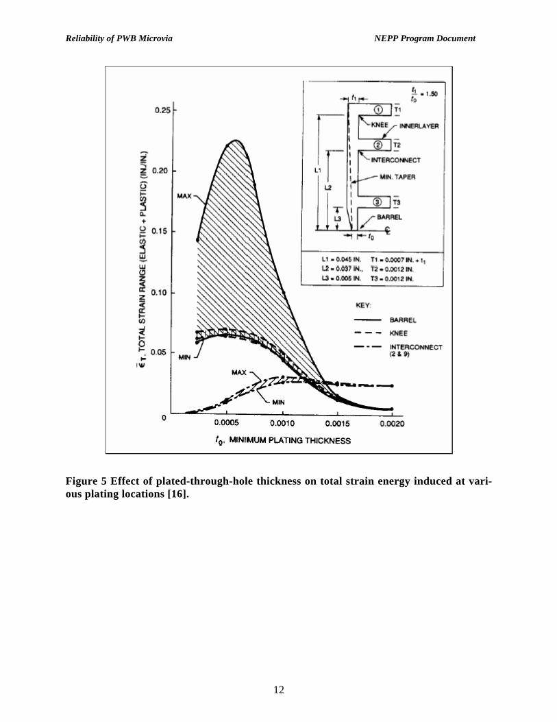
3.3.4 PTH Thermal Cycle Reliability Improvement Numerous publications and industry joint efforts cover the key parameters that affect thermal cycle reliability [1-2, 15-17]. The strain accumulation depends on strain level induced at each thermal cycle excursion. To increase the useful life cycle, the following approaches can be implemented: • Decrease the PTH aspect ratio (board thickness/PTH diameter) to less than 5:1 if possi-
ble. Aspect ratios higher than 10:1 (especially for less than 15 mil diameter hole size) are not recommended because of the difficulty of achieving adequate plating thickness in the center of the barrel
• Increase the Cu plating thickness, thus increasing the distance that a fatigue crack must propagate. For higher thickness/aspect ratio, the thickness needs to be optimized for proc-ess and various failure mechanisms. Optimize the process to reduce stress risers due to defects such as voids in Cu plating and at the PTH knee. The effect of plating thickness on induced strain energy due to thermal cycling and the number of cycles is shown in Figures 5 and 6 [16, 1].
• Improve and test for the adhesion of Cu foil and the laminate • Choose a Cu material with higher ductility and lower strength, balancing the two. • Decrease or eliminate thermal shocks during board processing such as preheating the
board before hot-air leveling, wave soldering, rework, etc. • Decrease the range of thermal cycling specifically avoiding exposure to temperatures
above the Tg of the resin. • Decrease the thermal expansion of the PWB over the thermal cycling by choosing a mate-
rial—such as polyimide— with a higher Tg and lower CTE.
11
Reliability of PWB Microvia NEPP Program Document
Figure 5 Effect of plated-through-hole thickness on total strain energy induced at vari-ous plating locations [16].
12

Reliability of PWB Microvia NEPP Program Document
Figure 6 Effect of plated through hole thickness on the number of thermal cycles to fail-ure and failure mechanism [1]. Numerous task groups from the IPC have performed round-robin tests to address many of these issues. These include. • PTH barrel cracking has been studied and the results reported in IPC-TR-579: “Round
Robin Reliability Evaluation of Small Diameter Plated Through Holes in Printed Wiring Boards” [17].
• Cu foil characteristics have been reported in IPC-TR-484: “Results of IPC Copper Foil Ductility Round Robin Study”
• For “gross” failure, thermal stress with microsectioning is performed per IPC-TM-650, “Thermal Stress of Plated-Through-Hole”,
13

Reliability of PWB Microvia NEPP Program Document
• For “finer” failure, monitoring of a larger number of PTH samples, and objective results with numerical value, the IST test can be use which is documented in IPC-TM-650, Method 2.6.26.
4. Microvia Technologies High density interconnects (HDIs) constitute the newest layering connection approach for multilayer PWBs and substrates in electronic packaging that accommodate dense and fine pitch package and die requirements. The high density requirement is achieved by using much smaller via (microvia) structures. Microvias are vias of less than or equal to 6 mils (150 µm) in diameter used as blind and buried vias to form interconnections through one dielectric layer within a PWB. Microvias are cost effective and more reliable when used in outer layers in a blind via construction where the outer layers of a multilayer PWB are connected to the next adjacent signal layer. 4.1 Advantages of Microvia Technology Microvias offer several distinct advantages [1-3] over their mechanically produced counter-parts (see 4.2 below) from both the aspect of physical features and electrical performance, including the following: • Microvia within the pads (via-in-pad) allow significant reduction in fan out and routing
and therefore increased packaging density for assembly with a reduced layer count, greater layout efficiency, and improved cost effectiveness for a given PWB.
• PWBs with microvias enable the designer to incorporate the newest high density pack-ages and die into their system. The microvia is especially valuable, and may even be re-quired, when using parts such as full array packages, CSPs, and flip chip direct attach (FCDA) designs. PWBs with conventional through-hole fabrication technology have physical size limitations that cannot support parts with fine line geometry.
• PWBs with microvias show better electrical performance and signal integrity due to their physical structure. As the physical size of microvias becomes smaller and shorter, both the inductance and capacitance decrease, resulting in a reduction in switching noise.
• RFI/EMI/ESD (Radio Frequency Interference/Electromagnetic Interference/ Electrostatic Discharge) can be improved by effective grounding. Increased routability area combined with the microvias-in-pad implementation enable a designer to utilize more ground plane around the component thus reducing the ground return loop.
• Proven microvia technology yields higher reliability because of the significantly lower area aspect ratio (1:1) due to its fabrication in one dielectric layer when compared to a larger drilled through-hole via having a much high aspect ratio (>10:1).
4.2 Microvia Fabrication Techniques Vias are formed by many methods, PTHs are normally made by mechanical drilling followed by plating, whereas microvias are often made by other processes, including chemical means and ablation even though for larger microvias new advanced drilling techniques specifically
14

Reliability of PWB Microvia NEPP Program Document
developed for this purpose can be used. Because of chemical and ablation limitations, the mi-crovia layers generally do not have glass reinforcement that provides the rigidity needed for handling and end use structural requirement. With advancement in ablation techniques and materials, new procedures are being developed to address this limitation. The key methods of fabricating vias are the following: • Advanced mechanical drilling • Laser drilling with UV-YAG, CO2 or UV excimer • Photo definition processing with unsupported photosensitive dielectric • Plasma etching using a microwave-induced gas plasma Fabrication of non-drilled microvias may have additional conductive materials replacing ei-ther the copper foil or copper metallization. Mechanical drilling has traditionally been the most widely practiced method of hole creation, However, for creating microvias its use is now limited. It cannot be used to generate mi-crovias and even if it could, its isotropic drilling feature is undesirable. The vertical walls of mechanically drilled holes are straight up and down, making them less desirable for the sub-sequent plating operations. Other fabrication methods generate anisotropic walls with open-ings at the top allowing better wall metallization. The process steps for three major methods of fabricating nonmechanically drilled microvias are shown schematically in Figure 7. The processes involved are as follows: • Laser ablation. The laser-ablated formation of vias currently requires the use of non-glass
reinforced laminate, such as aramid or resin coated copper (RCC) for the dielectric. Three different drilling options for forming microvias are in use: (1) Transverse excitation in at-mospheric pressure, (2) Excimer laser, and (3) Nd:YAG (Neodymium:Yttrium-Aluminum Garnet) laser. The industry is making major strides to improve the throughput with lasers to make the cost more competitive with mass generation techniques such as photo and plasma vias.
• Photovia technology. The photovia approach is based on a photoimaged dielectric, usually a resin, and pattern plating to form the via and circuitry connections. The different photovia approaches can be broken down into three categories determined by the metallization proc-ess: (1) panel plate, (2) pattern plate and (3) full-build pattern plate.
• Plasma etching. Plasma-etched vias rely on the use of copper clad non-glass reinforced lami-nate, such as polyimide or epoxy resin coated copper (RCC) for the dielectric. The copper foil is used as a conformal mask to define the via openings in the process.
Paste via technology is another category that is widely used to produce via interconnections for commercial applications. Two common technologies in this category are ALIVHTM (Any-Layer Interstitial Via Hole, a trade mark of Matsushita Electric Industry, see [1]) and B2itTM (Buried Bump Interconnection Technology, a trademark of Toshiba).
15

Reliability of PWB Microvia NEPP Program Document
The ALIVH process uses nonwoven aramid prepreg as its dielectric material and copper paste for the hole filling. The build-up process is not sequential; rather, it uses layer pairs and aramid-epoxy prepreg with copper-paste vias that can be laminated at one time into a three-dimensional structure. Six to 10 layers have been laminated in this way. This technology has been used for cellular phone fabrication in many of its functions including the keypad integrated into one card. This type of structure is up to 20 percent lighter than normal FR-4 epoxy fiberglass multilayers. B2it uses glass-reinforced prepreg for rigid and liquid crystal resin for flexible PWBs and silver paste for holes. This process does not require conventional or microvia drilling equipment since vias are formed by displacing the glass cloth and resin during lamination. Currently, the design rule and features focus on consumer products, but it is anticipated to be implemented for simple PBGA fabrication in the future.
Rigid Core HDI layer/DielectricResin or photo Copper Foil
Rigid Core HDI layer/DielectricResin or photo Copper Foil
PhotoviaPlasmaviaLaservia
Figure 7 Schematic drawing showing key process steps in the fabrication of three non-drilled microvias [Adapted from Ref 3].
4.3 Laservias
LASER is an acronym for Light Amplification by Stimulated Emission of Radiation and it is based on the principle that electric energy is converted into a high energy-density coherent light beam by means of stimulation and amplification. A wide variety of materials can be laser drilled, but the speed and therefore the throughput of the drilling process depends on the material proper-ties. In general two main ways are used to maximize the throughput: 1) Reduce the Cu layer thickness to 5 µm (1/8 oz.) to allow the rapid removal of the copper
16

Reliability of PWB Microvia NEPP Program Document
2) Develop substrate materials having good laser ablation characteristics. For example, Ther-mount® containing non-woven aramid fiber or the use of RCC thin Cu foils (min. 5 µm) covered with an epoxy resin laminated on both sides of a rigid substrate.
Lasers are beginning to dominate microvia formation technology for several reasons that in-clude:
• The laser beam simulates an electronic drill bit, but has a critical advantage ⎯as mechanical drill bits become smaller, cost and breakage drastically increases and speed decreases. For lasers, a smaller beam size means faster and cheaper production.
• Laser beam diameters offer choices from 1- to 10-mil holes, with energy choices for one- or two-level blind vias, and the same flexible programmable via placement capability that makes mechanical drilling so attractive.
• "Laser-friendly" materials, glass-free, also provide superior circuit performance; the thinner the copper the better laser penetration.
Thus, the key advantages of laser drilling are capability, productivity, flexibility, and maximum throughput. These characteristics of lasers allow the broadened use of deposited dielectric mate-rials, and they are not restricted only to photo-imageable materials. The following factors have hindered the higher use of laser technology by PWB fabricators: • They are not a drop-in replacement for mechanical drilling machines.
• Their optimal use requires the employment of different laminate materials and circuits, and a new design cycle implementation and participation by the OEM.
• The capital cost is high, a few times higher than that of a new six-spindle drilling machine.
• Adoption of a new technology requires consideration of other issues including rapid technol-ogy obsolescence, cost of training, familiarization, and compatibility.
Lasers are classified primarily by their wavelength and power outputs as shown in Figure 8. The nature of laser emission, for example, the wavelength, fluence (measured in joules per square centimeter), peak power, pulse width, and pulse rate, is different, and therefore different process-ing and quality is achieved depending on the type of materials considered for ablation. A number of laser systems currently being used for drilling PWBs and flex substrates are as follows: UV (ultraviolet) lasers: • Excimer laser • Neodymium-doped: Yttrium-Aluminum-Garnet ((Nd:YAG) laser • Neodymium-doped: Yttrium-Lithium-Fluorine (Nd:YLF) laser
17

Reliability of PWB Microvia NEPP Program Document
IR (infrared) lasers: • Continuous Wave Carbon Dioxide (CW CO2) laser • Transverse Excited Atmospheric Carbon Dioxide (TEA CO2) laser • Sealed Radio Frequency Excited Carbon Dioxide (Sealed RF Excited CO2) laser
Figure 8 Light wavelength and its relation to laser type [1]. Figure 9 shows that the laser spot size resolution is directly related to laser wavelength [18]. The shorter the wavelength, the smaller the feature size that can be formed by a laser. UV and IR la-ser systems are now widely used to generate microvias in PWBs and flex circuits. Even though UV lasers have slower processes, they generally can produce vias of higher quality with finer feature sizes, virtually ready to be plated without post processing. For this reason, UV diode pumped solid-state (UV-DPSS, e.g., Nd:YAG) lasers are becoming the choice for flex substrates such as polyimide film microvia generation and producing specific features by removal. On the other hand, CO2 IR lasers are used to remove dielectric materials and in general cannot be used to ablate copper, even though there has been some attempt in expanding their applications. Because of the high ablation requirement for copper ablation, the laser thermal loading causes delamination. This disadvantage becomes a benefit when it comes to removing dielectrics, as the laser becomes self-limited when it “hits” the copper land. In addition, the IR lasers are not able to remove copper, and they are also slow in removing FR-4 laminate material. The strengths and weaknesses of each laser system should be considered for specific application. The two key systems that are currently widely used for generating microvias in PWB and flex substrates are further discussed in the following.
18
Reliability of PWB Microvia NEPP Program Document
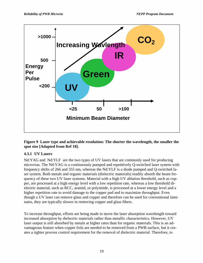
Figure 9 Laser type and achievable resolution: The shorter the wavelength, the smaller the spot size [Adapted from Ref 18].
4.3.1 UV Lasers Nd:YAG and Nd:YLF are the two types of UV lasers that are commonly used for producing microvias. The Nd:YAG is a continuously pumped and repetitively Q-switched laser system with frequency shifts of 266 and 355 nm, whereas the Nd:YLF is a diode pumped and Q-switched la-ser system. Both metals and organic materials (dielectric materials) readily absorb the beam fre-quency of these two UV laser systems. Material with a high UV ablation threshold, such as cop-per, are processed at a high energy level with a low repetition rate, whereas a low threshold di-electric material, such as RCC, aramid, or polyimide, is processed at a lower energy level and a higher repetition rate to avoid damage to the copper pad and to maximize throughput. Even though a UV laser can remove glass and copper and therefore can be used for conventional lami-nates, they are typically slower in removing copper and glass fibers. To increase throughput, efforts are being made to move the laser absorption wavelength toward increased absorption by dielectric materials rather than metallic characteristics. However, UV laser output is still absorbed by metals at higher rates than for organic materials. This is an ad-vantageous feature when copper foils are needed to be removed from a PWB surface, but it cre-ates a tighter process control requirement for the removal of dielectric material. Therefore, to
<25 50 >100
UV Green
CO2
IR
>1000
Increasing Wavlength
500 Energy Per Pulse
<200
Minimum Beam Diameter
19

Reliability of PWB Microvia NEPP Program Document
remove dielectric material by a typical high energy focused UV beam laser with a short wave length, first a window in the conformal mask must be generated by either chemical etching or vaporization by UV at approximately the same location. In addition, the small beam diameter needs to trepan, i.e., to move the laser beam in a spiral way to drill holes larger than the laser fo-cal spot. These additional processes significantly increase laser processing time and increase cost for a blind microvia formation. For these reasons, UV-DPSS lasers are usually used to process smaller microvia features generally less than 50 µm in diameter.
4.3.2 IR Lasers The IR CO2 laser with its long wavelength and its natural tendency to be reflected by metallic material, especially copper, is excellent for drilling organic polymers. The two types of CO2 la-ser systems are the Sealed RF Excited CO2 and the TEA CO2 laser. There are other laser sys-tems, but they are not effective in drilling a broad range of dielectric materials. In addition, they are expensive to run, hard to control or they are not appropriate to drill large panel areas.
4.3.3 Hybrid Drilling In 1998, hybrid laser drilling, enabling parallel processing of both a UV and CO2 laser on a PWB, was introduced to solve the registration issues common in the CO2 conformal mask drill-ing method. This technique allows the copper and dielectric to be processed in parallel, meaning that while the UV laser removes copper, creating the via size and shape desired, the CO2 follows behind, removing the dielectric that is uncovered. CO2 lasers efficiently remove dielectrics, even non-homogeneous, glass-reinforced dielectrics. However, the CO2 laser alone cannot create small vias (say below 75 µm) and cannot remove copper, aside from limited success in removing pre-treated thin foils 5µm and below. The UV laser can be used to create very small vias and re-move all common copper foils from 3 µm up to 36 µm (1 oz. Cu), and even plated foils. UV la-sers alone can also remove dielectrics but the material removal rate is slow. Moreover, the re-sults are generally poor for non-homogeneous materials such as glass-reinforced FR4s because the glass can only be removed if the energy density is increased to levels that can damage the inner-layer stop pad.
4.4 Photovias
Photovias take advantage of the behavior of photoimageable dielectric (PID) materials. When exposed to ultraviolet light, these materials will polymerize and will not dissolve by solvent so-lution. If via holes are not exposed due to photomasks, then when processed they will be dis-solved away by the solution. The process is similar to use of a solder mask when it is used to clear out an area around an SMT pad. This allows the use of most existing solder mask process-ing equipment, thus avoiding the necessity of a large capital equipment investment for imple-mentation. Contrary to laser drilling, this type of process is amenable to mass production (batch processing). In addition, both dry and liquid-resist techniques are in use giving another selection option.
20

Reliability of PWB Microvia NEPP Program Document
PID technologies were initially developed as an alternative to multilayer lamination as a way to make multilayer PWBs [1]. PID technology builds up each surface signal layer on top of the pre-vious layers in a sequential approach. The base under all built-up layers is a conventional dou-ble-sided or multilayer circuit board containing voltage, ground planes, and even signal layers. Mechanically drilled and plated-through holes are used only in the core layers and to make con-nections to the built-up layers, but holes do not extend through these layers. Liquid and dry PID applications are processed differently. The former requires two unique pieces of equipment: a coater of some variety and a leveling tool, whereas the latter requires a vacuum laminator. The two types of PID applications also provide slightly different via wall pro-files. The liquid PID has tapered via walls, whereas the dry-film PID has vertical via walls. Ta-pered walls provide good plating coverage on the via walls and base. Vertical walls allow for a smaller via top opening and correspondingly smaller capture land for a given via bottom diame-ter. The earliest widely practiced PID for microvia build-up technology is Surface Lamina Circuits (SLC®) developed in the early 1990s. Flip-chip direct chip attach (FC/DCA) and PWBs utilizing SLC technology were shipped by IBM Yasu (Japan) and Endicott in 1992 and 1995, respec-tively. SLC was initially developed and implemented with a liquid photoimageable solder mask and later with a dry-film PID mask having almost identical electrical properties.
4.5 Plasmavias
Plasmavia etching evolved from the traditional process of plasma desmearing of through- holes prior to electroless Cu plating. The plasma is generated in a partial vacuum filled with a mixture of oxygen, nitrogen, and chlorofluorocarbon gases. The principal chlorofluorocarbon used is tetrafluoromethane (CF4). Microwave magnetrons create the plasma field and special low-frequency kilowave units help provide rapid etching of organics. The PWB manufacturing process of plasmavias generally utilizes commonly practiced PWB techniques; only the via generation process is different. In the production of plasma-etched via holes, two or three process steps replace the conventional mechanical drilling, deburring, and desmearing steps: (1) the location and geometry of the via holes are photographically defined, (2) openings are etched in the copper foil that serve as the resist mask, and (3) for blind vias, the thickness of the copper foil is reduced to eliminate the copper overhang. In addition to drilling, plasma etching can also be used to sculpture the substrate surface or to fabricate slots, grooves, stepped windows, etc. The oldest example of a process creating plasmavias is DYCOstrate®. The process was first em-ployed for high-reliability military, aerospace, medical, and IC packaging. It utilizes a core mate-rial of polyimide film with plasma-etched holes, drilled epoxy fiberglass, or other plasma-etchable materials such as liquid crystal polymers or RCC foils. Multiple layers can be built to increase the density with buried and blind vias.
21

Reliability of PWB Microvia NEPP Program Document
The plasma etching process is basically an isotropic process with undercut, but because of the small dimensions involved, plating problems do not typically occur. When the etching depth is increased, as in the case of blind vias, the resulting undercut is generally too big to allow reliable plating. The problem is overcome through copper reduction: etching the copper foil, eliminating the copper overhang, and providing a thinner copper foil for fine-line resolution.
4.6 Laservias Compared to other Vias
Table 2 shows the compatibility of via formation by the three techniques, i.e., laser, photo, and plasma, on four basic surface dielectric structures [1]. Laser vias can be produced in all four structures, whereas use of the other two techniques are limited. This is one reason why laservias are more widely used today.
Table 2 Compatibility of via formation by various techniques.
NoNoYes?NoPlasma Via
YesYesYesYesLaser Via, Yag
YesYesYes?Yes?Laser Via, CO2
YesNoNoNoPhoto Via
PhotoimageableResin
Thermally Curable Resin
RCCStandard Configuration
NoNoYes?NoPlasma Via
YesYesYesYesLaser Via, Yag
YesYesYes?Yes?Laser Via, CO2
YesNoNoNoPhoto Via
PhotoimageableResin
Thermally Curable Resin
RCCStandard Configuration
Figure 10 shows a comparison on via formation cost between laservia and photovia technologies having a cross-over depending on the number of vias produced [19]. The higher cost of laservia is due to the sequential nature of the laser drilling process, the cost increasing linearly with in-creasing via count. On the other hand, the cost of photovia formation remains constant due to simultaneous mass via formation, even though process control and via reliability issues need to be addressed. Lasers are ideal primarily due to their high-resolution processing capabilities, fast processing speeds, reliability, versatility, and lower cost-of-ownership.
22

Reliability of PWB Microvia NEPP Program Document
Number of Microvias
CO
ST
Laser Photo
Number of Microvias
CO
ST
Laser Photo
Figure 10 Cost comparison of laservia and photovia technologies for microvia formation—laser technology is the least costly for low volume production (Adapted from [19]).
5. Specifications IPC is a good source for reviewing HDI guideline documents, design rules, materials, and test specifications. A few key standards are given below. • Figure 11 shows the hierarchy of IPC performance and qualifications including IPC-6016;
which contains the general specification for high density substrates not already covered by other documents.
• IPC-2315, the purpose of which is to provide guidelines for HDI technology, including edu-cating users in microvia formation, selection of wiring density, selection of design rules, in-terconnecting structures, and materials characterization. A number of design rules for various categories adopted from this specification are listed in Table 3.
• IPC-4104, the purpose of which is to identify materials used for HDI structures. A series of specifications are defined for specific available materials, each outlines engineering and per-formance data that could be used for ordering.
• IPC-TM-650-2.6.26, in which the 2.6.26 test provides guidelines on changes in resistance measurements of PTH/PTV when subjected to thermal cycling. IST coupons (designed by In-terconnect Solution Inc.) are used to provide application of DC current through the intercon-nections. The number of cycles to failures provides a qualitative assessment of the perform-ance of all interconnections. Test 2.6.8 provides the PTH/PTV interconnection resistance to thermal cycling effects of extreme heat due to heat exposed during the assembly, rework, and repair process.
23

Reliability of PWB Microvia NEPP Program Document
Figure 11 Hierarchy of IPC qualifications and specifications for PWBs.
Table 3 Example of HDI design rules illustrated in IPC-315.
Feature High yield/ Low cost µm (mil)
Common µm (mil)
Top-level fab-ricator
µm (mil)
Exotic fabri-cator
µm (mil) Microvia hole diameter at target land, no plating
125-200 (5-8) 100-200 (4-8) 75-250 (3-10) 35 (1.5) min
Microvia diameter at cap-ture land
350 (14) 300 (12) 250 (10) 150 (6)
Trace spacing on rigid outerlayer
125 (5) 100 (4) 87 (3.5) 5 (2)
Minimum HDI dielectric thickness
75 (3) 62.5 (2.5) 50 (2) 25 (10)
Minimum aspect ratio < 1.0 1.0 1.0 1.3 min Minimum plated thickness 25 (1) 25 (1) 30 (1.2) 30 (1.20)
6. Microvia Reliability Microvia reliability covers two key areas: (1) the reliability of PWB with microvias as formed and its resistance to normal assembly processes and subsequent user applications, and (2) after assembly, the effects of via-in-pad microvias on solder voids and the effect of the via structure on use conditions, including exposures to thermal and mechanical exposures. In late 1990, ITRI (the former R&D division of the IPC) established limitations in size fabrication and relative reli-ability of various microvias. Below, more recent investigations on this subject given in the litera-
24

Reliability of PWB Microvia NEPP Program Document
ture are first discussed and then the results of thermal cycle testing performed at JPL by this au-thor will be presented.
6.1 Voids arising from Microvias during Assembly
One of the main assembly issues for the microvia in pad (ViP) microvias is the formation of voids in solder joints. Blind ViP is the most efficient routing to accommodate high density inter-connect especially for area array packages with pitches lower than 0.8 mm pitches. Voids can results when gases trapped in microvias do not escape during reflow. Hajinder [20] and Grano et alia [21] investigated the effects of package pitch size, board design including microvia sizes, surface finish, and assembly process parameters on the formation of voids. Their findings for tin-lead solder are the following: • With the exception of 1.27 mm BGAs, as the pitch decreased so did the occurrence of voids. • The smaller the microvia size, the smaller the void size. The centered and off-design mi-
crovias had the most voids. whereas the copper-filled and inverted microvias showed virtu-ally no voids.
• ENIG surface finish PWBs tend to generate more voids compared to IAg (immersion silver) and OSP finish; ENIG with 25% higher voids than IAg. In addition, with ENIG, voids were present at the component site after 1st reflow and moved to the PWB site after 2nd reflow.
• A reflow profile with extended soak above 150°C and a lower peak reflow temperature and a shorter reflow time were all effective to some extent in reducing voids. On the other hand, solder paste type, solder particle size, and double-pass paste printing had a minimum effect on voiding. The addition of silver to tin-lead eutectic solder paste decreased void size.
• The 4 mil ViP accounted only for 6% of the total voids whereas the 6 and 8 mil ViPs had equally high void percentages with 40% and 46%, respectively. Microvias with one layer of depth accounted only for 12% of the total voids, whereas those with 3 layers of depth (layer 1 to layer 3) accounted for 56% of the total voids.
• The thinner the PWB, the more voids produced. For SnAgCu (SAC) solders, the voiding rate arising from microvias was studied by simulation [22]. It was shown that the lowest voiding was for Sn95.5Ag3.8Cu0.7 and Sn95.5Ag3.5Cu1.5. The voiding rate increased with decreasing Ag content from Ag3.5, mainly due to increasing sur-face tension. Voiding arising from microvias was governed by via filling and exclusion of fluxes. The voiding rate decreased with decreasing surface tension and increasing wetting force which in turn was dictated by the solder wetting or spreading. Both low surface tension and greater sol-der wetting prevented the flux from being entrapped within the microvias. A fast wetting speed might also facilitate reducing voiding. However, this factor is considered not as important as the final solder coverage area.
6.2 Microvia Failure Mechanisms
Microvias as part of the PWB design are exposed to thermal stresses during manufacturing and applications. These exposures may be either prolonged at an elevated temperature or isolated or
25

Reliability of PWB Microvia NEPP Program Document
with repeated temperature cycles. These exposures could lead to PWB and microvia failures. The most important sources of thermal stresses are: • Thermal shocks and thermal cycles during PWB manufacturing. The thermal shock occurs
when an assembly is exposed to rapid changes of temperature causing transient temperature gradients, warpage, and stresses within the part and/or assembly. The rate of temperature change for thermal shock is usually greater than 20°C/minute (see for example IPC-9701A [23]). Processes that can induce this rate of temperature change are solder mask cure and HASL (hot-air solder leveling).
• Thermal shocks and cycles occurring during assembling the PWB. Examples are glue cure, solder reflow, wave soldering, and rework using soldering irons, hot air, or molten solder in a pot.
• Thermal cycles in service. Depending on the application, these can be sever or mild, but in-clude temperature changes from inside to outside the electronic box and component local temperature rises due to functioning internal electronics.
Two key issues are important in reliability of microvias. These are (1) the continuity of plated microvias providing interlayer connections and (2) the insulation among different nets. Similar to the PTH, but to a lesser extent, microvia failures occur due to thermal strains induced due to CTE mismatch between the plated microvia and the resin. Scanlan et alia [24] investigated manufacturing issues and board level reliability for a 0.4 mm pitch FPBGA where microvias exist both in the package substrate and the PWB. Results were compared after thermal cycling, drop testing, and mechanical bending. ViP package substrates showed better resistance to thermal cycling by 20% relative to NViP package substrates. Failures were both microvia and solder joint cracking (see Figure 12). ViP/NViP combination showed excellent drop performance with the first failure after 148 drops whereas ViP-ViP combination showed poor performance with failure after 7 drops. In contrast, the best bend cycling results were for the ViP-ViP followed by the NViP-ViP combinations.
Figure 12 Package via crack and solder joint crack during drop test (See [24]). Jonnaalagadda [25] investigated the effect of ViP on the mechanical cycle bending behavior for 196 I/O Globtop PBGA packages with 1 mm pitch that were assembled on PWBs with ViP
26

Reliability of PWB Microvia NEPP Program Document
structure. Test results in conjunction with finite element analysis indicated that the ViP structure by itself does not pose a reliability risk. However, increase in applied loads could induce dielec-tric cracking that in turn can lead to trace and via failures. The proximity of microvias to PTHs and their effect on the reliability of microvias was evaluated by Primavera et alia [26] using different vendors and exposure to liquid-liquid thermal shock (LLTS) in the range of –55°/125°C with 10 second transitions. Results indicate (see Table 4) that the maximum failures were from the vias at a distance of 40 mils (60 mils center to center dis-tance from 20 mils PTH) from the PTHs. In addition, few failures were found in the vias at the distance of 5 mils from the PTH. The first failure was after 1100 LLTS cycles.
Table 4 Thermal cycle resistances of microvias for various via formation [26]. Via Hole Formation Technology
Dielectric Material Failure Mechanism
YAG Laser Glass Reinforced No failure to 2000 LLTS (–55°/125°C, 10 s transition)
YAG Laser Non Reinforced Crack at the Via Pad Interface YAG + CO2 Laser Glass Reinforced Improper Cleaning of the Glass Fibers
Crack Through the Via Photodefined Non Reinforced Crack at the Via Pad Interface
Andrews et al [27] observed intermittent opens during electrical testing for a specific lot of high-end PWB assemblies having double-sided SMT. Using an IR technique, they were able to nar-row failures to microvias. Cross-sectioning revealed a target pad to copper plating separation at the bottom of the microvias. Further investigation showed that a small percentage of microvias exhibited barrel cracks, and sometimes knee corner cracks. An IST study was conducted to determine the most effective testing parameters. After five cycles of preconditioning of coupons at 230°C, they were tested to maximum temperatures of 150°C, 170°C, 190°C, 210°C, and 220°C. The mean cycles to failures were 1000, 789, 464, 76, and 44 cycles, respectively. For the 190°C maximum temperature dwell, the mean cycles to failure was less than 500 cycles; therefore, this temperature was selected for subsequent thermal cycling for lead-free board process assembly. Failure for 210°C and above include those of knee crack, ma-terial delamination/break down, and barrel cracks that are considered to be the testing artifacts and therefore these temperatures are unacceptable for qualification techniques intended to repre-sent realistic environments. Phenolic-based FR-4 coupons with microvia passed 1000 IST thermal cycles at 190°C after five times at 230°C. The effect of the lead free reflow profile at 260°C conditioning on microvia deg-radation was severe. The coupons that were able to achieve 788 cycles at 150°C were reduced to a mean of 443 after 6 times at 230°C cycle and only 4 cycles after lead free preconditioning, six times at 260°C. Bora [28] evaluated ALVIH-G board technology used for cell phones having a double stack of microvias on the outer layers. The microvias were laser drilled, and the interconnection was con-
27

Reliability of PWB Microvia NEPP Program Document
ductive copper paste. The typical design rule is 100/100 microns line/space and 200/400 Via/Land. The reliability was investigated of double-sided surface mount assembly through 2 reflow operations and one rework using an 8-layer thin board (0.8 mm thick) epoxy-glass with low moisture absorption instead of aramid that has a higher moisture absorption. Assemblies with BGA passed 500 thermal shocks in the range of –25°C to 125°C and a 1000 hour humidity test at 85°C/85%. Cross-sectioning revealed graininess of solder after thermal shock with no separation of the microvia connection to the capture pad. In addition, no layer-to-layer separation was observed when the phone level drop test was performed at 1.5 meters on a hard vinyl sur-face.
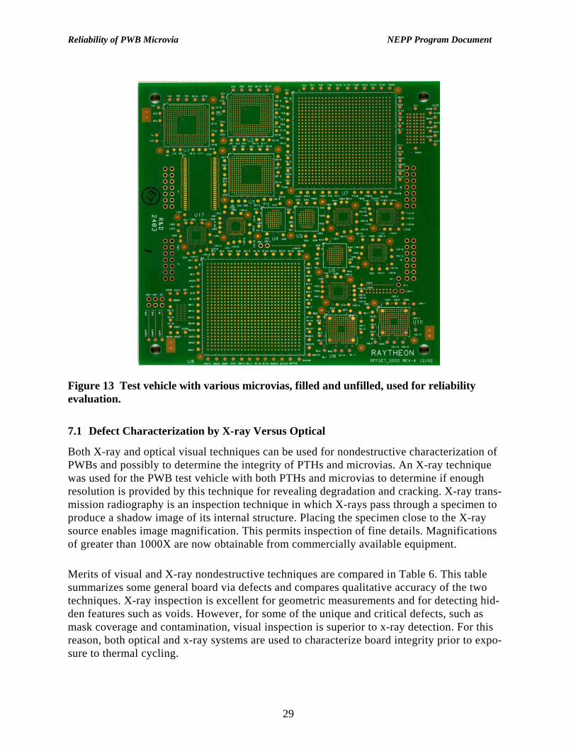
7. Thermal Cycle Characterization of PWB with Microvia and PTH In the early 2000s, a new test vehicle was designed and built by JPL-led Consortium covering both PTHs and microvias with and without filling materials. Figure 13 shows features of this test vehicle. The board includes BGA and FPBGA packages from 0.4 to 1.27 mm pitches with I/Os varying from 48 to 784. A TSOP package with 54 I/Os was used as control. Table 5 lists a sum-mary of packages and the types of microvias designed for the test vehicle. Plated-through-hole via-in-pads 8 mil in diameter were used only on 784 I/O BGA pads. Except for the 3 mil mi-crovia diameter for one design of a 192 I/O FPBGA with 0.4 mm pitch, the rest had 4 mil mi-crovias. Daisy chain microvias, however, had sizes as low as 2 mil and also included 3 and 4 mil microvias either filled or nonfilled as well as 8 mil ViPs. The daisy chain microvias and ViPs were monitored during thermal cycling. Table 5 List of packages, PTHs, PTHViPs, and microvias for the Consortium test vehicle.
Ref Des Nomenclature Pitch Definition Via Dia.& Definition
U1 FPBGA_280_CNF 0.8mm CNF=control non filled 4-mil (100-µm)-µviaU2 FPGA_280_ONF ONF=offset non filled 4-mil (100-µm)-µviaU3 FPBGA_280_RNF RNF=runout non filled 4-mil (100-µm)-µviaU4 FP_CSP_48_CSP 0.8mm CNF=control non filled 4-mil (100-µm)-µviaU5 FP_CSP_48_ONF ONF=offset non filled 4-mil (100-µm)-µviaU6 FP_CSP_48_RNF RNF=runout non filled 4-mil (100-µm)-µviaU7 784_FC_BGA 1.27mm C8F=control -8mil- filled 8-mil (200-µm) -THVIP*U8 784_FC_BGA_ONF ONF=offset non filled 4-mil (100-µm)-µviaU9 KY_144_.8 0.8mm CNF=control non filled 4-mil (100-µm)-µvia
U10 KY_144_.8_RNF RNF=runout non filled 4-mil (100-µm)-µviaU11 FPBGA_192_C4NF 0.4mm C=control-4mil via non filled 4-mil (100-µm)-µviaU12 FPBGA_192_O4NF O=offset-4mil via non filled 4-mil (100-µm)-µviaU13 FPBGA_192_R4NF R=Runout-4mil via non filled 4-mil (100-µm)-µviaU14 FPBGA_192_C3NF C3NF=control -3mil via non filled 3-mil (75-µm) - µviaU15 FPBGA_192_C3F C3F=control -3mil via filled 4-mil (100-µm)-µviaU16 FPBGA_192_C4F C4F=control -4mil via filled 4-mil (100-µm)-µviaU17 TSOP_54 0.8mm CNF=control non filled 4-mil (100-µm)-µvia
28
Reliability of PWB Microvia NEPP Program Document
Figure 13 Test vehicle with various microvias, filled and unfilled, used for reliability evaluation.
7.1 Defect Characterization by X-ray Versus Optical
Both X-ray and optical visual techniques can be used for nondestructive characterization of PWBs and possibly to determine the integrity of PTHs and microvias. An X-ray technique was used for the PWB test vehicle with both PTHs and microvias to determine if enough resolution is provided by this technique for revealing degradation and cracking. X-ray trans-mission radiography is an inspection technique in which X-rays pass through a specimen to produce a shadow image of its internal structure. Placing the specimen close to the X-ray source enables image magnification. This permits inspection of fine details. Magnifications of greater than 1000X are now obtainable from commercially available equipment. Merits of visual and X-ray nondestructive techniques are compared in Table 6. This table summarizes some general board via defects and compares qualitative accuracy of the two techniques. X-ray inspection is excellent for geometric measurements and for detecting hid-den features such as voids. However, for some of the unique and critical defects, such as mask coverage and contamination, visual inspection is superior to x-ray detection. For this reason, both optical and x-ray systems are used to characterize board integrity prior to expo-sure to thermal cycling.
29

Reliability of PWB Microvia NEPP Program Document
Table 6 Key solder defect types and ability to detect visible joints.
Visible Features X-ray Inspection
Visual Inspection
Mask coverage 0 +++ Contamination 0 +++ Mask coverage + +++
Short in conductors/Layers +++ 0 Microvia/PTH Voids +++ 0
Cu cracks in microvia/PTH + 0 +++ Excellent detection
++ Good detection 0 Poor or unacceptable
The use of destructive techniques is limited to research study for the characterization of fail-ure mechanisms, or when investigating the root cause of a field failure. Destructive tech-niques commonly include cross-sectioning combined with optical inspection, and SEM and EDX. A number of PTHs and microvias were cross-sectioned after thermal and reflow cycles to determine the integrity and damage levels in correlation to daisy-chain electrical test re-sults.
7.2 Inspection before Environmental Test
PWBs from two lots were chosen for inspection and subsequent environmental tests. Because of the cutting edge microvia technology built into the design, the first batch was considered unacceptable even though the actual quality of most microvias was acceptable. Only a limited number of ViPs for finer pitch CSPs exhibited unacceptable pad breakages. The second batch was of higher quality and considered to be acceptable for use in assembly. Both types of PWBs were inspected by optical microscopy and X-ray to document their quality and defect types. Figure 14 shows optical photomicrographs of acceptable and unacceptable (bottom) mi-crovias chosen from the two PWB lots. A number of microvias were designed with a daisy-chain configuration to monitor their integrity during environmental testing. Figure 15 shows representative daisy-chaining in three photomicrographs taken by optical microscopy and x-ray. Apparent in the figure are two of the daisy-chain microvias (filled) with 3 and 4 mil di-ameters showing darker images by X-ray, whereas the 2 mil microvias are unfilled (top row daisy chain). Resistance changes of these and other daisy chains were monitored during envi-ronmental tests to determine the number of cycles to failure.
30

Reliability of PWB Microvia NEPP Program Document
Figure 14 Optical photomicrographs of acceptable (top) and unacceptable microvias.
31

Reliability of PWB Microvia NEPP Program Document
4 Mil Microvia Filled
3 Mil Microvia Filled
2 Mil Microvia Non Filled
8 Mil Via in Pad, Filled
4 Mil Microvia, Filled
Figure 15 X-ray and optical photographs of daisy-chain microvias, filled (dark) and un-filled vias.
7.3 Environmental Test-Thermal Cycle Profiles
Industry has proposed several specific test coupons and thermal cycling test methods with various temperature ranges and rates in order to standardize testing conditions for PWBs with PTHs and more recently for microvia characterization and qualification. However, there are no proposed approaches for effective screening tests similar to those performed for high per-formance hybrid packages that cover both extreme hot and cold conditions. Such screening tests should be able to effectively discriminate behavior between an acceptable and unaccept-able PWB with microvias. Most qualification tests for commercial applications consider cost effectiveness and engineering efficiency and attempt to provide a test with the shortest possi-ble test period. For solder joints under thermal cycling, the dominant failure mechanisms are creep and re-laxation. Adequate high temperature dwells as specified by IPC-9701A are necessary for temperature stabilization, but dwell is of less importance for PWB evaluation where the PWB is made of polymeric materials with less dependency on creep. For PWBs, however, exces-sive dwell at high temperatures may cause excessive resin polymerization, consequently ren-dering the board more susceptible to brittle fracture. The ramping rates of heating and cool-ing are usually limited by the capacity of the environmental test chamber.
32
Reliability of PWB Microvia NEPP Program Document
The PWB test vehicle shown in Figure 13 covered various daisy-chain PTHs and microvias representative of those also included in the pads of various design patterns for large to small pitch packages. This enables monitoring of daisy chains during cycling and compares the re-sults with those included in pads after environmental tests. The key question, however, is what kinds of test methods and thermal cycle profiles provide meaningful test results for mi-crovia technology? One thermal cycle profile specifically chosen here is Condition C of Mil-Std-883 in the range of –65° to 150°C. The cold and hot temperatures are –15°C cooler and +25°C hotter than the oven standard thermal shock test. However, its maximum temperature is lower than the 190°C recently recommended for IST testing. The delta T for this temperature profile, how-ever, is larger than any of the tests listed in Table 1. This temperature range is considered to be severe, but not sufficiently excessive to cause unacceptable failures. Indeed, hybrid pack-ages are required to be qualified to this temperature range. In addition, especially for high reliability applications, this profile is not severe since at assembly level, assemblies may be required to be subjected to –55°C/125°C. Therefore, a temperature regime more severe than this is suitable at a lower level, i.e., PWB characterization. Another thermal cycle regimen uses the solder reflow profile since the PWBs are required to be exposed to at least one re-flow cycle, but are required to meet three such cycles covering double-sided and rework re-quirements. The reflow profile is extremely severe, but it is a realistic requirement even though each reflow cycle may be equivalent to hundreds of use condition cycles.
7.4 Tg and Capability for Lead-free Reflow Temperature
Since there was minor PWB damage due to 100 thermal cycles, representative samples from a cycled PWB, SN01, were characterized for Tg, CTE, and extreme thermal cycles. The ex-pansion variation and therefore Tg, CTEs in x/y/z, and exposure to thermal cycling in the range of –150°C to +275°C were all carried out using suitable thermal mechanical analysis (TMA) equipment. Generally, high stress in a PWB via or microvia occurs due to through-thickness (z direction) thermal expansion during a thermal excursion. Figure 16 shows thermal expansion (CTE) for the z, x, and y directions, respectively. The CTE for the z direction is 43.21 ppm, which is about three times that of the y and x directions having values of 14.62 and 12.83 ppm, respectively. Above the Tg, the CTE in the z direction significantly increases and become 297.7 ppm. The Tg of the PWB is about 145°C (146.71°C). The Tg experiences significant changes detected at about 260°C. After exposure to this temperature, sample was cooled to RT, and it was noticed that the PWB had delami-nated. It was presumed that at lower temperatures—even with repetitive exposure—delamination would not occur.
33

Reliability of PWB Microvia NEPP Program Document
Z-CTEZ-CTE
X-CTEX-CTE Y-CTEY-CTE
Figure 16 The x, y, z CTEs by TMA for a thermal-cycled PWB. The peak reflow temperature was reduced to 245°C, representive of a lead-free solder joint assembly. Again, the TMA technique was used to determine microvia behavior under this and a lower extreme temperature using a thermal cycle in the range of –100°C to 245°C. Three thermal cycles were executed, while at the same time dimensional changes due to thermal cycling were continuously monitored by TMA. There was a small deviation in CTEs during the 2nd cycle, but the deviation disappeared during the 3rd cycle. Visual inspection after 1, 2, and 3 cycles revealed no delamination. Figure 17 compares samples from this (bottom photo) and the previous one with thermal excursion to 260°C. No delamination was noted for the 245°C max temperature reflow.
34

Reliability of PWB Microvia NEPP Program Document
Figure 17 Condition of TMA samples: the top one exposed to one cycles (–100° to +275°C); the bottom one exposed to 3 thermal cycles (–100° to +245°C).
8. Summary and Findings Key issues and findings from the literature survey and test results are summarized in the fol-lowing:
• HDI technology with 6 mil or lower size microvias is required to meet the finer pitch area array package implementation.
• Area array packages with 1.27 mm pitch are beginning to be implemented in NASA systems. As pitch grows smaller in value, the need for using a high density PWB with microvias becomes a necessity for the internal I/O routing.
• For conventional multilayer PWB and array packages with 1-1.27 mm pitch, PTHs can be used. However, it should be born in mind that the most common thermally induced board failures are due to PTHs.
• Thermal shock oven testing and accelerated tests, including HATS and IST, are now commonly used by industry to effectively qualify PWBs with and without microvia technology.
• To detect microvia failures by the IST method in a realistic time, it is recommended to use 190°C as the maximum thermal cycle temperature rather than the lower maximum temperature of 150°C normally used for conventional multilayer PWBs.
35

Reliability of PWB Microvia NEPP Program Document
• For NASA systems with unique and low volume requirements, laser microvia technol-ogy is preferred over the photovia and plasma etching technologies.
• Industry has already developed specifications for microvia technology. Refer specifi-cally to IPC-2315 for guidance for HDI and IPC-4104 for the HDI material identifica-tion.
• Microvia reliability involves two aspects: failures due to routine PWB microvia forma-tion and subsequent assembly processes, and failures due to void formation in the sol-der with subsequent failure during field thermal and mechanical exposures.
• Regarding microvia reliability, in the late 1990s ITRI (once part of IPC but now dis-solved) with industry-wide participation performed a microvia fabrication feasibility and reliability investigation.
• Again, regarding microvia reliability, only limited work has been performed by others. The effect of various board and manufacturing parameters on ViP void formation at board sites, the combination of ViP/NViP in package substrates and ViP/NViP on PWBs, and the effect of distance of microvias to PTHs are among the various microvia issues that have been investigated.
• Test vehicles were built in early 2000 having ViP microvias from 2 to 4 mils. Some mi-crovias were filled, whereas others were nonfilled. These, as well as 8 mil THViPs, were characterized and subjected to environmental testing.
• Visual inspection using optical microscopy was more effective in determining the con-dition of the microvias than X-rays. X-ray radiography clearly identified filled vias but was of limited value for detecting other conditions.
• Thermal cycling in the range of –65°/150°C was used to characterize reliability of vari-ous microvia sizes.
• Cross-sectional examination after 100 thermal cycles revealed failure for 2 mil mi-crovias, but no failures for any other vias.
• TMA characterization of cycled PWBs revealed that the Tg of the test board was about 150°C with delamination starting at 260°C.
• TMA was also used to thermal cycle specimens between –100°C and 245°C. The latter temperature is representative of the maximum temperature for a lead-free assembly. Af-ter 3 cycles, no delamination was observed. The samples exposed to 260°C, however, did exhibit delamination.
9. Recommendations Microvia technology is a viable option if microvias are needed for HDI implementation. Re-liability data for commercial use are scarce and nonexistent for space application. Our ther-mal cycle test results—based on a very limited sample size—indicate that laser microvia sizes as low as 4 mils are reliable and therefore have promise for use in high reliability appli-cation. The effect of via in pad (ViP) on voiding and solder joint reliability was not investi-gated. Therefore, further work is required to further define such effects.
36
Reliability of PWB Microvia NEPP Program Document
10. List of Acronyms ALIVH Any-Layer Interstitial Via Hole BGA Ball Grid Array B2it Buried Bump Interconnection Technology BOK Body of Knowledge CBGA Ceramic Ball Grid Array CCGA Ceramic Column Grid Array CGA Column Grid Array COTS Commercial-off-the-shelf CSP Chip Scale (Size) Package CTE Coefficient of Thermal Expansion CTF Cycles to Failure Cu Copper DPSS Diode Pumped Solid-State EDX Energy Dispersive X-Ray ENIG Electroless Nickel Immersion Gold FCBGA Flip Chip Ball Grid Array FPBGA Fine Pitch BGA, a.k.a. Chip Scale Package (CSP) FC/DCA Flip-Chip Direct Chip Attach HASL Hot-Air Solder Leveling HATS Highly Accelerated Thermal Shock HDI High Density Interconnect IAg Immersion Silver ILS Inner-Layer Separation I/O Input/Output IPC Association Connecting Electronics Industries IR Infrared IST Interconnect Stress Test KGD Known Good Die LASER Light Amplification by Stimulated Emission of Radiation LCCC Leadless Ceramic Chip Carrier LLTS Liquid-Liquid Thermal Shock MER Mars Exploration Rover Nd:YAG Neodymium-doped:Yttrium-Aluminum-Garnet Nd:YLF Neodymium-doped:Yttrium-Lithium-Fluorine NEPP NASA Electronic Parts and Packaging
37
Reliability of PWB Microvia NEPP Program Document
Ni Nickel NViP Non-Via in Pad OSP Organic Solder Preservative PBGA Plastic Ball Grid Array PCQR2 Process Capability, Quality, and Relative Reliability PID Photoimageable Dielectric PTH Plated-Through Hole PTHV Plated-Through Hole Via PTHViP Plated-Through Hole Via-in-Pad PWA Printed Wiring Assembly PWB Printed Wiring Board QFP Quad Flat Pack RCC Resin Coated Copper RT Room Temperature SAM Scanning Acoustic Microscopy SEM Scanning Electron Microscopy SMT Surface Mount Technology TCE Also CTE, Thermal Coefficient of Expansion Tg Glass Transition Temperature THViP See PTHViP TMA Thermal Mechanical Analysis TSM Thermal Shock Method TSOP Thin Small Outline Package UV Ultraviolet ViP Via in Pad
11. Acknowledgements The research described in this paper was carried out at the Jet Propulsion Laboratory, California Institute of Technology, under a contract with the National Aeronautics and Space Administra-tion. Reference herein to any specific commercial product, process, or service by trade name, trademark, manufacturer, or otherwise, does not constitute or imply its endorsement by the United States Government or the Jet Propulsion Laboratory, California Institute of Technol-ogy. The author extends his appreciation to the JPL-led Consortia, especially to James Russell at R&D Circuits, and many others at JPL who contributed to the progress of these activities. Sin-cere thanks go to the NASA program mangers and GSFC of the NASA Electronic Parts and Packaging Program (NEPP) including Michael Sampson, Dr. Charles Barnes, and Phillip Zu-lueta for their continuous support and encouragement.
38

Reliability of PWB Microvia NEPP Program Document
12. References 1. Coombs, C.F.,Printed Circuits Handbook, 5th Edition (McGraw-Hill, New York, 2001). 2. Lau, J., Ricky Lee, R., Microvias for Low Cost, High Density Interconnects (McGraw-Hill,
2000). 3. IPC/JPCA-2315, "Design Guide for High Density Interconnects (HDI) and Microvias," IPC,
June 2000. 4. Fjelstad, J., Ghaffarian, R., Kim, Y-G., Chip Scale Packaging for Modern Electronics (Elec-
trochemical Publications, 2002). 5. Ghaffarian, R., “Thermal cycle Reliability of PBGA/CCGA 717 I/Os,” Proceedings of IEEE
Electronic Components and Technology (2006). 6. Ghaffarian, R., “Chip Scale Package Assembly Reliability”, Chapter 23rd in Area Array In-
terconnect Handbook, Puttlitz, K.and Totta, P., eds. (Kluwer Academic Publishers, 2002). 7. Ghaffarian, R., “BGA Assembly Reliability,” Chapter 20, Area Array Packaging Handbook,
Gilleo, K., ed. (McGraw-Hill, 2002). 8. Fillion, R.A., Daum, W., Wildi, E.J., and Kaminsky, E.B., “Multichip Modules- Chip First
vs. Last Analysis,” Proceedings of ISHM International Symposium on Microelectronics, San Francisco, CA (October 1992) p, 391 (see ref 1).
9. Boetttcher, L., Ostmann, A., Neumann, A., Reichl, H., “Integration of Active and Passive Components Using Chip-in-Polymer Technology,” Proceedings of Surface Mount Interna-tional (Chicago, 2005).
10. Sauter, K., “Thermal Stress Testing and Impact on High Thermal Excursion Pre-Conditioning on Cycles to Fail,” Proceedings of APEX Conference, (Anaheim, 2006).
11. Freda, M., Barker,D., “Predicting Plated Through Hole Life at Assembly and in the Field from Thermal Stress Data,” Proceedings of APEX Conference, (Anaheim, 2006).
12. http://www.polarinstruments.com/support/reliability/ap307.pdf. 13. http://www.Hats-Tester.com. 14. http://www.pcbquality.com/. 15. Knadle, K., Jadhav, V., “Proof is in the PTH- Assuring Via Reliability from Chip Carriers to
Thick Printed Wiring Boards,” Proceeding of IEEE Electronic Components and Technology (2005).
16. Iannuzelli, R. “Predicting Plated-Through-Hole Reliability in High Temperature manufac-turing Process” ASME Conference Proceedings (Nov., 1994).
17. IPC-TR-579, “Round Robin Reliability Evaluation of Small Diameter Plated Through Holes in Printed Wiring Boards”.
18. Venkat, S.,Hanon, T. “Laser Processing−The Future of HDI Manufacturing,” SEMICON West 2000 (San Francisco, 2000).
19. Liu, F., et al, “Reliability Assessment of Microvia in HDI Printed Circuit Boards,” IEEE Transaction on Component and Packaging Technology (June 2002) Vol 25, pp 254-259.
20. Harjinder, L., Sethuraman, S., “SMTA, Assembly issues with Microvia Technologies,” Journal of SMT, Vol. 17 Issue 1 (2004).
21. Grano,F., Bruno, F., Kor,D., O’Keefre, D., “Impact of Microvia-in-pad dressing on void for-mation,” Proceedings of Surface Mount International (Chicago, 2003).
22. Dasgupta, A., Huang, B., Lee, N., “Effect of Lead-Free Alloys on Voiding at Microvia,” IPC Printed Circuits Expo, APEX (2004).
39

Reliability of PWB Microvia NEPP Program Document
23. IPC-9701A, “Performance Test Methods and Qualification Requirements for Surface Mount Solder Attachments”. Published by IPC (Association Connecting Electronics Industries).
24. Scanlan, J., Syed, A., Kang, W., Abe, M., “Assembly and Board Level Reliability Consid-erations for 0.4mm Pitch Ball Grid Array Packages,” Proceedings of IEEE Electronic Com-ponents and Technology (2005).
25. Jonnaalagadda, K., “Reliability of Via-in-Pad Structures in Mechanical Cycling Fatigue,” Microelectronics Reliability, 42 (2002) pp, 253-258.
26. Primavera,A., Joshi, J., “The Proximity of Microvias to PTHs and Its Impact on the Reli-ability,” http://www.uic.com/wcms/images2.nsf/(GraphicLib)/hdi2001.pdf/$File/hdi2001.pdf.
27. Andrews, P., Parry, G., Reid, P., “Microvia Reliability Concerns in the Lead Free Assembly Environment,” IPC Works 2005 (2005).
28. Bora, M.,“Qualification of ALIVH Boards for Handset Assembly,” IMAPS 2005 (2005).
40


![PWB Handbook[1]](https://img.dokumen.tips/doc/110x75/577d25b71a28ab4e1e9f734a/pwb-handbook1.jpg)