Embed Size (px)
Citation preview
Copyright © 2016 RelChip, Inc. All rights reserved.
RC10001 USER MANUAL
RelChip, Inc.
RC10001 User Manual Preface
March 2016 Copyright © 2016 RelChip, Inc. All rights reserved. ii
PREFACE
ABOUT THIS MANUAL
This manual is for those who program the RC10001. It is not a programming language manual, but instead a detailed description of registers, memory, and the core. The first portion of the manual describes the RC10001 operation, and the second portion describes the internal periphery. We include sufficient information to correctly program the RC10001; however, the user should refer to the appropriate assembler or compiler references for their chosen development system.
CONVENTIONS
Textual
Embedded in the text are changes in fonts to aid the reader. They are:
Bold: Used for register and pin names. Italic: Used for example terminology. For example, reg [31:0] could be used to represent any of the
general-purpose registers (possibly R0 [31:0] or R1 [31:0]). Italic Underline: Links within the document.
Assembly Code
Assembly code conventions are:
Bold Used for a register name or assembly mnemonic. {…} Used for Optional Entries. […] is used to identify values used to generate an address, i.e. [R6, #5] Italics denote registers selected from a set (identified in the text). This can also include register
lists and special registers. Register lists are registers surrounded by {} as follows: o Comma Separated Lists, i.e. {R2, R4, R6}, these execute in ascending order. o Ranges, i.e. {R2-R6} o Combinations of the above, i.e. {R0-R2, R5, R6-R7}
#imm {i} is an immediate value of “{i}” bits width. #lab{i} is a label resolved into “{i}” bits of offset
Pin Names
Pin Names are always in bold capital letters. Generally, pins ending in “n” are low active.
RC10001 User Manual Preface
March 2016 Copyright © 2016 RelChip, Inc. All rights reserved. iii
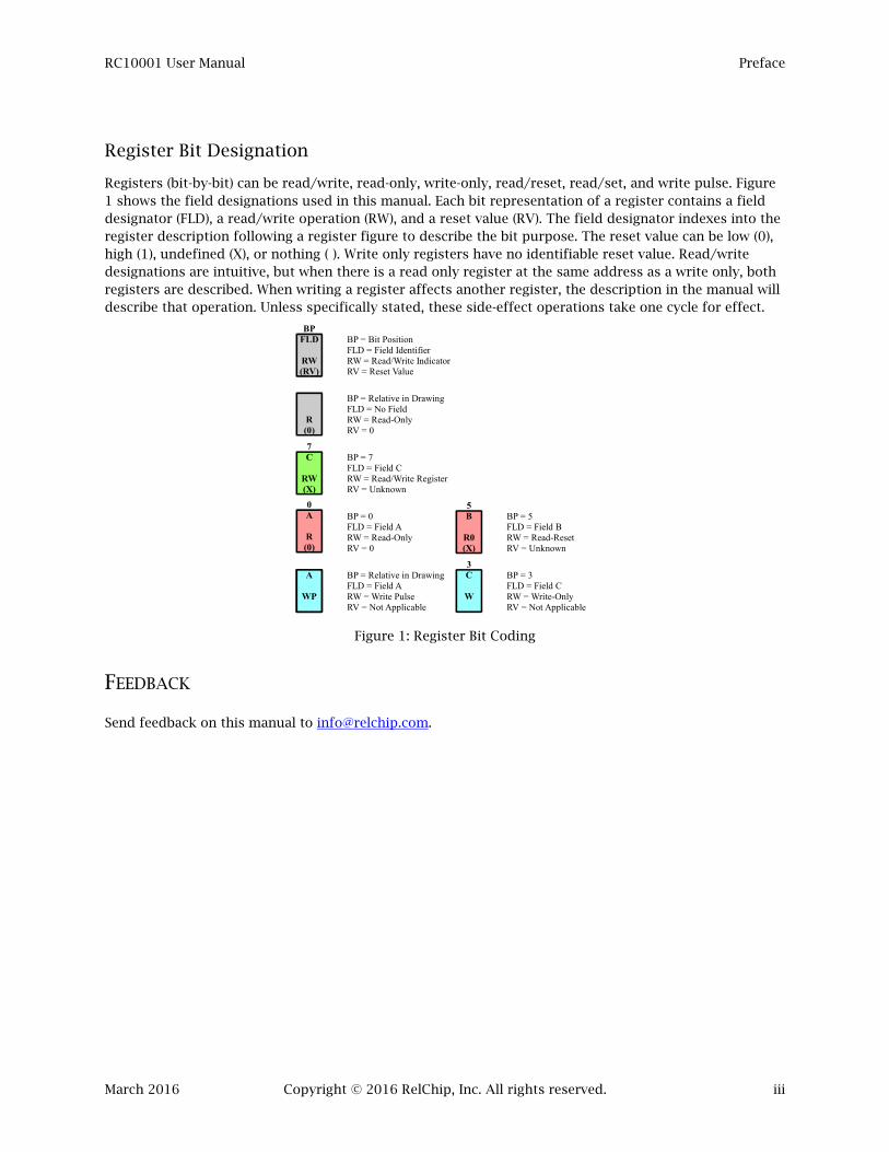
Register Bit Designation
Registers (bit-by-bit) can be read/write, read-only, write-only, read/reset, read/set, and write pulse. Figure 1 shows the field designations used in this manual. Each bit representation of a register contains a field designator (FLD), a read/write operation (RW), and a reset value (RV). The field designator indexes into the register description following a register figure to describe the bit purpose. The reset value can be low (0), high (1), undefined (X), or nothing ( ). Write only registers have no identifiable reset value. Read/write designations are intuitive, but when there is a read only register at the same address as a write only, both registers are described. When writing a register affects another register, the description in the manual will describe that operation. Unless specifically stated, these side-effect operations take one cycle for effect.
Figure 1: Register Bit Coding
FEEDBACK
Send feedback on this manual to [email protected].
R(0)
BPFLD
RW(RV)
7C
RW(X)
0A
R(0)
5B
R0(X)
A
WP
3C
W
A
WP
BP = Bit PositionFLD = Field IdentifierRW = Read/Write IndicatorRV = Reset Value
BP = Relative in DrawingFLD = No FieldRW = Read-OnlyRV = 0
BP = 7FLD = Field CRW = Read/Write RegisterRV = Unknown
BP = 0FLD = Field ARW = Read-OnlyRV = 0
BP = Relative in DrawingFLD = Field ARW = Write PulseRV = Not Applicable
BP = 5FLD = Field BRW = Read-ResetRV = Unknown
BP = 3FLD = Field CRW = Write-OnlyRV = Not Applicable
RC10001 User Manual Table of Contents
March 2016 Copyright © 2016 RelChip, Inc. All rights reserved. iv
TABLE OF CONTENTS
Preface .................................................................................................................................................................................. ii
About This Manual ......................................................................................................................................................... ii
Conventions ..................................................................................................................................................................... ii
Textual .......................................................................................................................................................................... ii
Assembly Code ............................................................................................................................................................ ii
Pin Names ..................................................................................................................................................................... ii
Register Bit Designation ........................................................................................................................................... iii
Feedback .......................................................................................................................................................................... iii
Table of Contents .............................................................................................................................................................. iv
Table of Tables .................................................................................................................................................................. xii
Table of Figures ............................................................................................................................................................... xiv
1 Overview ..................................................................................................................................................................... 18
2 The Cortex-M0 Processor ........................................................................................................................................ 20
2.1 Basics ................................................................................................................................................................ 20
2.2 Core Registers ................................................................................................................................................. 21
2.2.1 R12/SP - Stack Pointer Register .............................................................................................................. 21
2.2.2 MSP/PSP - Stack Pointer Registers ......................................................................................................... 21
2.2.3 PC - Program Counter Register ............................................................................................................... 22
2.2.4 PSR - Program Status Register ................................................................................................................ 22
2.2.5 PRIMASK – Priority Mask Register ......................................................................................................... 23
2.2.6 CONTROL - Control Register .................................................................................................................. 24
3 Exceptions and Interrupts ....................................................................................................................................... 25
3.1 Priority .............................................................................................................................................................. 27
3.1.1 Reset ............................................................................................................................................................. 27
3.1.2 Non-Maskable Interrupt (NMI) ................................................................................................................. 27
3.1.3 Hardfault ..................................................................................................................................................... 27
3.1.4 Supervisor Call ........................................................................................................................................... 28
3.1.5 Debug Monitor ........................................................................................................................................... 28
3.1.6 SysTick – System Tick Timer ................................................................................................................... 28
3.1.7 Peripheral Interrupts ................................................................................................................................ 28
3.2 Vector Table .................................................................................................................................................... 29
3.3 WFE/WFI – Wait for Event, Wait for Interrupt .......................................................................................... 30
3.4 ISR – Interrupt Service Routine Entry and Exit ......................................................................................... 30
3.4.1 Reset Entry Special Considerations ....................................................................................................... 30

RC10001 User Manual Table of Contents
March 2016 Copyright © 2016 RelChip, Inc. All rights reserved. v
3.4.2 Other Handler Entries ............................................................................................................................... 31
3.4.3 Exception Returns ..................................................................................................................................... 31
3.4.4 Exceptions and Multiple Word Operations ........................................................................................... 31
3.4.5 Chaining ...................................................................................................................................................... 32
4 Memory ....................................................................................................................................................................... 33
4.1 Memory Types ................................................................................................................................................ 33
4.2 Memory Regions ............................................................................................................................................. 33
4.2.1 Code Region ................................................................................................................................................ 33
4.2.2 SRAM Region .............................................................................................................................................. 34
4.2.3 Peripheral Region ...................................................................................................................................... 34
4.2.4 RAM Segments (2) ...................................................................................................................................... 34
4.2.5 Device Segments (2) .................................................................................................................................. 34
4.2.6 System Region ............................................................................................................................................ 34
4.2.7 Memory and Instruction Barrier Instructions ...................................................................................... 34
5 Power Management ................................................................................................................................................... 36
5.1 Cortex-M0 Core Sleep Modes ....................................................................................................................... 36
5.1.1 Sleep Mode .................................................................................................................................................. 36
5.1.2 Deep Sleep Mode ........................................................................................................................................ 36
5.1.3 Wait for Interrupt Wake Up-WFI ............................................................................................................. 36
5.1.4 Wait for Event Wake Up-WFE .................................................................................................................. 36
5.1.5 Sleep on Exception Exit ............................................................................................................................ 36
5.1.6 Deferred Exit from Sleep Mode ............................................................................................................... 37
5.1.7 “C” Functions .............................................................................................................................................. 37
5.2 Peripheral Clock Enable ................................................................................................................................ 37
5.3 Battery Backup ................................................................................................................................................ 37
6 Reset and Boot Methods .......................................................................................................................................... 38
6.1 Reset Options and Sources........................................................................................................................... 38
6.1.1 Power-On Reset (POR) ............................................................................................................................... 38
6.1.2 Hard Reset (HARDRESETn) ..................................................................................................................... 38
6.1.3 Soft Reset (SOFTRESETN) ........................................................................................................................ 39
6.1.4 Watchdog Timer Reset (WDT) ................................................................................................................. 39
6.1.5 Battery Backup Reset ................................................................................................................................ 39
6.1.6 System Software Reset ............................................................................................................................. 39
6.1.7 Debug Reset ................................................................................................................................................ 39
6.2 Boot Sources and Files .................................................................................................................................. 39
6.2.1 Boot Files and Records ............................................................................................................................. 39
6.2.2 Common Boot ROM Process .................................................................................................................... 40
6.2.3 SSP Interface Boot ...................................................................................................................................... 40

RC10001 User Manual Table of Contents
March 2016 Copyright © 2016 RelChip, Inc. All rights reserved. vi
6.2.4 UART Interface Boot ................................................................................................................................. 40
6.2.5 External Bus Boot ....................................................................................................................................... 40
6.2.6 Serial Wire Debug Boot ............................................................................................................................. 41
7 The Cortex-M0 Instructions .................................................................................................................................... 42
7.1 Condition Flags ............................................................................................................................................... 42
7.2 Alphabetical List ............................................................................................................................................. 43
7.2.1 Usage ............................................................................................................................................................ 47
8 SYSCON - System Configuration ............................................................................................................................ 93
8.1 System Configuration Registers .................................................................................................................. 93
8.1.1 SYSCON_BOOTCTRL - Boot Control Register ..................................................................................... 94
8.1.2 SYSCON_PRESETCTRL - Peripheral Reset Control Register ............................................................. 94
8.1.3 SYSCON_RSTSTAT - Reset Source Register ......................................................................................... 95
8.1.4 SYSCON_AHBCLKCTRL - Clock Enable Register ................................................................................ 96
8.1.5 SYSCON_AHBCLKDIV - System Clock Divisor Register .................................................................... 97
8.1.6 SYSCON_CLKOUTDIV - Clock Output Pin Divisor Register ............................................................. 97
8.1.7 SYSCON_SYSTCKCAL - System Tick Calibration Register ................................................................ 97
8.1.8 SYSCON_BATTCTRL - Battery Backup Control Register .................................................................. 98
8.1.9 SYSCON_DEVICEID - Device Identification Register .......................................................................... 98
9 NVIC - Nested Vectored Interrupt Controller ...................................................................................................... 99
9.1 Interrupt Priority ............................................................................................................................................ 99
9.2 Software Assertion of Interrupts ................................................................................................................ 99
9.3 NVIC Registers ............................................................................................................................................. 100
9.3.1 NVIC_ISER – Interrupt Set-Enable Register ....................................................................................... 101
9.3.2 NVIC_ICER – Interrupt Clear-Enable Register................................................................................... 102
9.3.3 NVIC_ISPR – Interrupt Set-Pending Register .................................................................................... 103
9.3.4 NVIC_ICPR – Interrupt Clear-Pending Register ................................................................................ 104
9.3.5 NVIC_IPR0 – Interrupt Priority 0 ........................................................................................................ 105
9.3.6 NVIC_IPR1 – Interrupt Priority 1 ........................................................................................................ 105
9.3.7 NVIC_IPR2 - Interrupt Priority 2 ......................................................................................................... 105
9.3.8 NVIC_IPR3 – Interrupt Priority 3 ........................................................................................................ 106
9.3.9 NVIC_IPR4 – Interrupt Priority 4 ........................................................................................................ 106
9.3.10 NVIC_IPR5 – Interrupt Priority 5 .................................................................................................... 106
10 IOCON - Input/Output Configuration.......................................................................................................... 107
10.1 Pads ................................................................................................................................................................ 107
10.2 Registers ....................................................................................................................................................... 108
11 GPIO - General Purpose Input/Output Ports .............................................................................................. 113
11.1 Operation ...................................................................................................................................................... 113
11.1.1 Masked Write ...................................................................................................................................... 113

RC10001 User Manual Table of Contents
March 2016 Copyright © 2016 RelChip, Inc. All rights reserved. vii
11.1.2 Masked Read ....................................................................................................................................... 114
11.2 Registers ....................................................................................................................................................... 115
11.2.1 GPIO_DATA - Masked Data Register ............................................................................................. 116
11.2.2 GPIO_DIR - Direction Register ........................................................................................................ 116
11.2.3 GPIO_IS – Interrupt Sense Register ................................................................................................ 117
11.2.4 GPIO_IBE – Interrupt Both Edges Register .................................................................................... 117
11.2.5 GPIO_IEV – Interrupt Event Register ............................................................................................. 118
11.2.6 GPIO_IE - Interrupt Enable Register ............................................................................................... 119
11.2.7 GPIO_RIS - Raw Interrupt Status Register .................................................................................... 119
11.2.8 GPIO_MIS - Masked Interrupt Status ............................................................................................. 120
11.2.9 GPIO_ICR - Interrupt Clear Register .............................................................................................. 120
12 RAMCFG - RAM Configuration ...................................................................................................................... 121
12.1 Registers ....................................................................................................................................................... 121
12.1.1 RAMCFG_IE - Interrupt Enable Register ........................................................................................ 121
12.1.2 RAMCFG_RIS - Raw Interrupt Status Register ............................................................................. 122
12.1.3 RAMCFG_MIS - Masked Interrupt Status Register ...................................................................... 122
12.1.4 RAMCFG_ICR - Interrupt Clear Register ....................................................................................... 122
12.1.5 RAMCFG_TM – Test Mode Register ............................................................................................... 123
13 EBCFG - External Bus Configuration ............................................................................................................ 124
13.1 Pin Description ............................................................................................................................................ 124
13.2 Operation ...................................................................................................................................................... 125
13.2.1 Thirty-two Bit Read Operations ...................................................................................................... 125
13.2.2 Thirty-two Bit Write Operations ...................................................................................................... 127
13.2.3 Parity .................................................................................................................................................... 128
13.2.4 Configuration and Status ................................................................................................................. 128
13.2.5 WAIT Options ..................................................................................................................................... 129
13.2.6 External Bus Interrupts ..................................................................................................................... 129
13.2.7 Eight-Bit Operations .......................................................................................................................... 129
13.2.8 Multiple Master Bus ........................................................................................................................... 130
13.3 External Memory And Input/Output Space ........................................................................................... 130
13.4 External Bus Configuration Registers ..................................................................................................... 130
13.4.1 EBCFG_CONFIG - Configuration Register ..................................................................................... 131
13.4.2 EBCFG_BUS_CONFIG - Bus Configuration Register .................................................................... 132
13.4.3 EBCFG_IE - Interrupt Enable Register ............................................................................................ 133
13.4.4 EBCFG_RIS - Raw Interrupt Status Register .................................................................................. 133
13.4.5 EBCFG_MIS - Masked Interrupt Status Register ........................................................................... 133
13.4.6 EBCFG_ICR - Interrupt Clear Register............................................................................................ 134
13.4.7 EBCFG_ERR_CONFIG - Error Configuration Register ................................................................. 134

RC10001 User Manual Table of Contents
March 2016 Copyright © 2016 RelChip, Inc. All rights reserved. viii
13.4.8 EBCFG_MIN_x/ EBCFG_MAX_x - Minimum and Maximum Chip Select Registers ............... 134
14 UART - Universal Asynchronous Receiver/Transmitter .......................................................................... 136
14.1 Features ......................................................................................................................................................... 136
14.2 Modes of Operation .................................................................................................................................... 136
14.2.1 RS-232 .................................................................................................................................................. 137
14.2.2 RS-485 .................................................................................................................................................. 137
14.2.3 LIN ......................................................................................................................................................... 138
14.2.4 Test Modes .......................................................................................................................................... 139
14.3 Pin Description ............................................................................................................................................ 139
14.4 Registers ....................................................................................................................................................... 140
14.4.1 UART_DLL – LSB Divisor Latch Register ....................................................................................... 141
14.4.2 UART_DLM – MSB Divisor Latch Register ..................................................................................... 141
14.4.3 UART_THR – Transmit Holding Register ..................................................................................... 141
14.4.4 UART_RBR - Receive Buffer Register ............................................................................................. 142
14.4.5 UART_IE – Interrupt Enable Register ............................................................................................. 142
14.4.6 UART_FCR – FIFO Control Register ............................................................................................... 143
14.4.7 UART_IIR – Interrupt Identification Register .............................................................................. 144
14.4.8 UART_LCR – Line Control Register ................................................................................................ 145
14.4.9 UART_MCR – Modem Control Register ......................................................................................... 146
14.4.10 UART_LSR – Line Status Register ................................................................................................... 147
14.4.11 UART_MSR – Modem Status Register ............................................................................................ 147
14.4.12 UART_SCR – Scratch Register ......................................................................................................... 148
14.4.13 UART_TER – Transmit Enable Register ........................................................................................ 148
14.4.14 UART_RS485CTRL – RS485 Control Register ............................................................................. 148
14.4.15 UART_RS485ADDR – RS485 Address Match Register ............................................................... 149
14.4.16 UART_RS485DLY – RS485 Turnaround Delay Register ............................................................ 149
14.4.17 UART_LCTL – LIN Control Register ............................................................................................... 149
15 SSP - Synchronous Serial Port ........................................................................................................................ 150
15.1 Signals ........................................................................................................................................................... 150
15.2 Interface Protocols ...................................................................................................................................... 151
15.2.1 Serial Peripheral Interface Protocol ................................................................................................ 151
15.2.2 Texas Instrument Synchronous Serial Protocol ........................................................................... 152
15.2.3 Semiconductor Microwire Protocol ................................................................................................ 153
15.3 Registers ....................................................................................................................................................... 153
15.3.1 SSP_CR0 – Control 0 Register .......................................................................................................... 154
15.3.2 SSP_CR1 – Control 1 Register .......................................................................................................... 155
15.3.3 SSP_DR – FIFO TX/RX Data Registers ............................................................................................ 156
15.3.4 SSP_SR – Status Register .................................................................................................................. 156

RC10001 User Manual Table of Contents
March 2016 Copyright © 2016 RelChip, Inc. All rights reserved. ix
15.3.5 SSP_PR – Pre-scale Register .............................................................................................................. 156
15.3.6 SSP_IE - Interrupt Enable Register .................................................................................................. 157
15.3.7 SSP_RIS - Raw Interrupt Status Register ....................................................................................... 157
15.3.8 SSP_MIS - Masked Interrupt Status Register ................................................................................ 158
15.3.9 SSP_ICR - Interrupt Clear Register ................................................................................................. 158
15.3.10 SSP_FCNT – FIFO Count Register .................................................................................................... 158
15.3.11 SSP_FCLR – FIFO Clear Register ...................................................................................................... 159
16 TIMER- Timer Counters .................................................................................................................................. 160
16.1 Timer 16 vs Timer 32 ................................................................................................................................. 160
16.2 Operations .................................................................................................................................................... 161
16.2.1 Match Operation ................................................................................................................................. 161
16.2.2 Capture Operation ............................................................................................................................. 164
16.2.3 UART/LIN Counter Mode .................................................................................................................. 164
16.3 Registers ....................................................................................................................................................... 165
16.3.1 TIMER_IR – Interrupt Register ........................................................................................................ 166
16.3.2 TIMER_TCR – Timer Control Register ........................................................................................... 166
16.3.3 TIMER_TC – Timer Counter Value Register ................................................................................. 167
16.3.4 TIMER_PR – Pre-scale Compare Register ...................................................................................... 167
16.3.5 TIMER_PC – Pre-scale Counter Register ........................................................................................ 168
16.3.6 TIMER_MCR – Match Control Register .......................................................................................... 169
16.3.7 TIMER_MR# – Match Registers ....................................................................................................... 170
16.3.8 TIMER_CCR – Capture Control Register ....................................................................................... 170
16.3.9 TIMER_CR0 – Capture Value Register ........................................................................................... 171
16.3.10 TIMER_EMR – External Match Register ......................................................................................... 171
16.3.11 TIMER_CTCR – Count Control Register ........................................................................................ 172
16.3.12 TIMER_PWMC – Pulse Width Modulator Control Register ........................................................ 172
16.3.13 TIMER_MOCR – Match Output Control Register ......................................................................... 173
16.3.14 TIMER_MOR – Match Output Register .......................................................................................... 173
17 RTC - Real Time Counter ................................................................................................................................ 174
17.1 Registers ....................................................................................................................................................... 174
17.1.1 RTC_MOD – Mode Register .............................................................................................................. 174
17.1.2 RTC_PR – Pre-scale Load Register .................................................................................................. 175
17.1.3 RTC_TIM – Time Register ................................................................................................................ 175
17.1.4 RTC_PC – Pre-scale Counter Register ............................................................................................ 176
17.1.5 RTC_ALM – Alarm Register ............................................................................................................. 176
17.1.6 RTC_IE - Interrupt Enable Register ................................................................................................ 177
17.1.7 RTC_RIS - Raw Interrupt Status Register ...................................................................................... 177

RC10001 User Manual Table of Contents
March 2016 Copyright © 2016 RelChip, Inc. All rights reserved. x
17.1.8 RTC_MIS - Masked Interrupt Status Register ............................................................................... 177
17.1.9 RTC_ICR Interrupt Clear Register .................................................................................................. 177
18 WDT - Watchdog Timer .................................................................................................................................. 178
18.1 Registers ....................................................................................................................................................... 178
18.1.1 WDT_MOD – Mode Register............................................................................................................. 178
18.1.2 WDT_TC – Time Out Register ......................................................................................................... 179
18.1.3 WDT_FEED – Feed Sequence Register ............................................................................................ 179
18.1.4 WDT_TV – Timer Value Register .................................................................................................... 179
19 SysTick - System Tick Timer .......................................................................................................................... 180
19.1 Registers ....................................................................................................................................................... 180
19.1.1 SysTick_CTRL – Control and Status Register .............................................................................. 180
19.1.2 SysTick _LOAD – Reload Value Register ...................................................................................... 181
19.1.3 SysTick _VAL – Current Value Register ........................................................................................ 181
19.1.4 SysTick _CALIB – Calibration Value Register .............................................................................. 181
20 CLKOUT – Clock Generator ............................................................................................................................ 182
21 Serial Wire Debug ............................................................................................................................................. 183
21.1 Serial Wire Debug Reset ............................................................................................................................. 183
21.2 Protocol ......................................................................................................................................................... 184
21.2.1 The Packet Request ............................................................................................................................ 184
21.2.2 Turnaround Cycle .............................................................................................................................. 184
21.2.3 Acknowledge ....................................................................................................................................... 185
21.2.4 Data Packet .......................................................................................................................................... 185
21.2.5 Host Write ............................................................................................................................................ 185
21.2.6 Host Read ............................................................................................................................................ 186
21.2.7 AP Posted Reads ................................................................................................................................. 186
21.2.8 READOK and RESEND ....................................................................................................................... 187
21.2.9 WAIT Status ......................................................................................................................................... 188
21.2.10 FAULT Status ...................................................................................................................................... 189
21.2.11 Protocol Errors.................................................................................................................................... 190
21.2.12 Write Data Parity Errors .................................................................................................................... 190
21.2.13 Sticky Flags .......................................................................................................................................... 190
21.3 Debug Port (DP) ........................................................................................................................................... 191
21.3.1 DP_IDCODE - Identification Code Register .................................................................................. 191
21.3.2 DP_ABORT - Abort Register ............................................................................................................ 192
21.3.3 DP_CTRL/DP_STAT - Control and Status Register .................................................................... 192
21.3.4 DP_WCR - Wire Control Register .................................................................................................... 192
21.3.5 DP_RDBUFF - Read Buffer Register ................................................................................................ 192
21.3.6 DP_SELECT - AP Select Register ...................................................................................................... 193

RC10001 User Manual Table of Contents
March 2016 Copyright © 2016 RelChip, Inc. All rights reserved. xi
21.3.7 DP_RESEND - Resend Register ........................................................................................................ 193
21.4 Access Port (AP) ........................................................................................................................................... 194
21.4.1 AP_CSW - Control/Status Word Register ...................................................................................... 194
21.4.2 AP_TAR – Transfer Address Register ............................................................................................ 195
21.4.3 AP_DRW - Data Read/Write Register ............................................................................................. 195
21.4.4 AP_BD0 to AP_BD3 - Banked Data Registers ............................................................................... 195
21.4.5 AP_CFG - Configuration Register ................................................................................................... 195
21.4.6 AP_BASE - Debug Base Address Register...................................................................................... 196
21.4.7 AP_IDR – Identification Register .................................................................................................... 196
21.5 Register Addressing .................................................................................................................................... 196
21.5.1 Data Watchpoint and Trace Unit (DWT) ........................................................................................ 197
21.5.2 Breakpoint Unit (BP) .......................................................................................................................... 200
21.5.3 SCB - System Control Block .............................................................................................................. 201
21.5.4 DCB - Debug Control Block .............................................................................................................. 205
22 Glossary ............................................................................................................................................................. 210
23 Index ................................................................................................................................................................... 213

RC10001 User Manual Table of Tables
March 2016 Copyright © 2016 RelChip, Inc. All rights reserved. xii
TABLE OF TABLES
Table 1: Little Endian Byte Storage ............................................................................................................................... 20 Table 2: Little Endian Halfword & Instruction Storage ............................................................................................. 20 Table 3: Cortex-M0 Core Registers ................................................................................................................................ 21 Table 4: Mnemonics for Program Status Register Combinations ........................................................................... 22 Table 5: Interrupts............................................................................................................................................................ 26 Table 6: Vector Table Entry Addresses ........................................................................................................................ 29 Table 7: Exception Return ............................................................................................................................................... 31 Table 8: Boot Options ...................................................................................................................................................... 38 Table 9: Instruction Set ................................................................................................................................................... 43 Table 10: Instruction Set Continued ............................................................................................................................. 44 Table 11: Instruction Set Continued ............................................................................................................................. 45 Table 12: Instruction Set Continued ............................................................................................................................. 46 Table 13: Conditional Execution Codes ....................................................................................................................... 55 Table 14: Special Registers ............................................................................................................................................. 73 Table 15: System Configuration Register Map ........................................................................................................... 93 Table 16: Boot System Memory Remap ........................................................................................................................ 94 Table 17: NVIC Register Map ....................................................................................................................................... 100 Table 18: SSP.TIMER16A/GPIO 0 IO Configuration Register Map ........................................................................ 108 Table 19: TIMER16B/TIMER32A/TIMER32B/GPIO 1 IO Configuration Register Map ...................................... 109 Table 20: TIMER32B/UART/GPIO 2 IO Configuration Register Map ................................................................... 109 Table 21: UART/EXBUS/GPIO 3 IO Configuration Register Map .......................................................................... 110 Table 22: EXBUS/GPIO 4 IO Configuration Register Map ...................................................................................... 110 Table 23: EXBUS/GPIO 5 IO Configuration Register Map ...................................................................................... 111 Table 24: EXBUS/GPIO 6 IO Configuration Register Map ...................................................................................... 111 Table 25: EXBUS/SWD/GPIO 7 IO Configuration Register Map ............................................................................ 112 Table 26: GPIO Write Logic .......................................................................................................................................... 114 Table 27: GPIO Read Logic ........................................................................................................................................... 114 Table 28: GPIO Register Memory Segment ............................................................................................................... 115 Table 29: GPIO Register Map ....................................................................................................................................... 115 Table 30: GPIO Interrupt Options .............................................................................................................................. 118 Table 31: RAM Configuration Register Map ............................................................................................................. 121 Table 32: External Bus Signals .................................................................................................................................... 124 Table 33: External Memory and Input/Output Space ............................................................................................. 130 Table 34: External Bus Configuration Register Map ............................................................................................... 131 Table 35: Reset Values for CS Address Range ......................................................................................................... 135 Table 36: UART Pinout ................................................................................................................................................. 139 Table 37: UART Registers ............................................................................................................................................ 140 Table 38: UART FIFO Trigger Level ............................................................................................................................ 143 Table 39: UART Interrupt Priorities ........................................................................................................................... 144 Table 40: UART Line Control Register Fields ........................................................................................................... 145 Table 41: UART Line Control Register Parity Fields ............................................................................................... 146 Table 42: SSP Interface Signals ................................................................................................................................... 150 Table 43: SSP Register Map .......................................................................................................................................... 153 Table 44: Timer/Counter Pins ..................................................................................................................................... 160 Table 45: Timer Register Addressing ........................................................................................................................ 165 Table 46: Real Time Clock Register Map ................................................................................................................... 174 Table 47: Watchdog Timer Register Map .................................................................................................................. 178 Table 48: SysTick Register Map .................................................................................................................................. 180

RC10001 User Manual Table of Tables
March 2016 Copyright © 2016 RelChip, Inc. All rights reserved. xiii
Table 49: Serial Wire Debug Acknowledge Responses ........................................................................................... 185 Table 50: Host Responses for DP Write Transactions ............................................................................................ 185 Table 51: Host Responses for AP Write Transactions ............................................................................................ 185 Table 52: Host Expectations from a DP Read Transaction .................................................................................... 186 Table 53: Host Expectations from an AP Read Transaction ................................................................................. 186 Table 54: DP Register Map ........................................................................................................................................... 191 Table 55: AP Register Map ........................................................................................................................................... 194 Table 56: System and Debug Address Space ........................................................................................................... 196 Table 57: DWT Register Map ....................................................................................................................................... 197 Table 58: Watchpoint Comparator Functions .......................................................................................................... 199 Table 59: BP Register Map............................................................................................................................................ 200 Table 60: SCB Register Address Map ......................................................................................................................... 201 Table 61: DCB Register Map ........................................................................................................................................ 205 Table 62: Register Selection ........................................................................................................................................ 208 Table 63: CPM Register Packing .................................................................................................................................. 208

RC10001 User Manual Table of Figures
March 2016 Copyright © 2016 RelChip, Inc. All rights reserved. xiv
TABLE OF FIGURES
Figure 1: Register Bit Coding ........................................................................................................................................... iii Figure 2: RC10001 Block Diagram ................................................................................................................................ 19 Figure 3: Stack Pointer Registers ................................................................................................................................... 21 Figure 4: Program Counter Register ............................................................................................................................. 22 Figure 5: Program Status Register ................................................................................................................................. 22 Figure 6: Application Program Status Register ........................................................................................................... 23 Figure 7: Execution Program Status Register .............................................................................................................. 23 Figure 8: Interrupt Program Status Register ............................................................................................................... 23 Figure 9: Priority Mask Register ..................................................................................................................................... 23 Figure 10: Control Register ............................................................................................................................................. 24 Figure 11: Memory Map ................................................................................................................................................... 35 Figure 12: Arithmetic Shift Right Example (Shift by Three) ..................................................................................... 53 Figure 13: Logical Shift Left Example (Shift by Three) .............................................................................................. 69 Figure 14: Rotate Right by Three Example .................................................................................................................. 79 Figure 15: SYSCON Boot Control Register ................................................................................................................... 94 Figure 16: SYSCON Peripheral Reset Control Register .............................................................................................. 94 Figure 17: SYSCON Reset Source Register ................................................................................................................... 95 Figure 18: SYSCON AHB Clock Control Register ........................................................................................................ 96 Figure 19: SYSCON System Clock Divisor Register .................................................................................................... 97 Figure 20: SYSCON Clock Output Pin Divisor Register ............................................................................................. 97 Figure 21: SYSCON System Tick Calibration Register ............................................................................................... 97 Figure 22: SYSCON Battery Backup Control Register ................................................................................................ 98 Figure 23: SYSCON Device Identification Register ..................................................................................................... 98 Figure 24: NVIC Interrupt Set-Enable Register ......................................................................................................... 101 Figure 25: NVIC Interrupt Clear-Enable Register ..................................................................................................... 102 Figure 26: NVIC Interrupt Set-Pending Register ...................................................................................................... 103 Figure 27: NVIC Interrupt Clear-Pending Register .................................................................................................. 104 Figure 28: NVIC Interrupt Priority Register #0 ........................................................................................................ 105 Figure 29: NVIC Interrupt Priority Register #1 ........................................................................................................ 105 Figure 30: NVIC Interrupt Priority Register #2 ........................................................................................................ 105 Figure 31: NVIC Interrupt Priority Register #3 ........................................................................................................ 106 Figure 32: NVIC Interrupt Priority Register #4 ........................................................................................................ 106 Figure 33: NVIC Interrupt Priority Register #5 ........................................................................................................ 106 Figure 34: IO Pad Circuit .............................................................................................................................................. 107 Figure 35: IOCON IO Configuration Register ........................................................................................................... 108 Figure 36: GPIO Masked Data Register (GPIO0 to GPIO6) ...................................................................................... 116 Figure 37: GPIO 7 Masked Data Register .................................................................................................................. 116 Figure 38: GPIO Direction Register (GPIO 0 to 6) .................................................................................................... 116 Figure 39: GPIO 7 Direction Register ......................................................................................................................... 116 Figure 40: GPIO Interrupt Sense Register (GPIO 0 to 6) ......................................................................................... 117 Figure 41: GPIO 7 Interrupt Sense Register .............................................................................................................. 117 Figure 42: GPIO Interrupt Both Edges Register (GPIO 0 to 6) ............................................................................... 117 Figure 43: GPIO 7 Interrupt Both Edges Register .................................................................................................... 117 Figure 44: GPIO Interrupt Event Register (GPIO 0 to 6) ......................................................................................... 118 Figure 45: GPIO 7 Interrupt Event Register .............................................................................................................. 118 Figure 46: GPIO Interrupt Enable Register (GPIO 0 to 6) ....................................................................................... 119 Figure 47: GPIO 7 Interrupt Enable Register ............................................................................................................ 119 Figure 48: GPIO Raw Interrupt Status Register (GPIO 0 to 6) ............................................................................... 119

RC10001 User Manual Table of Figures
March 2016 Copyright © 2016 RelChip, Inc. All rights reserved. xv
Figure 49: GPIO 7 Raw Interrupt Status Register .................................................................................................... 119 Figure 50: GPIO Masked Interrupt Status Register (GPIO 0 to 6) ......................................................................... 120 Figure 51: GPIO 7 Masked Interrupt Status Register .............................................................................................. 120 Figure 52: GPIO Interrupt Clear Register (GPIO 0 to 6) .......................................................................................... 120 Figure 53: GPIO 7 Interrupt Clear Register ............................................................................................................... 120 Figure 54: RAM Interrupt Enable Register ................................................................................................................ 121 Figure 55: RAM Raw Interrupt Status Register ........................................................................................................ 122 Figure 56: RAM Masked Interrupt Status Register .................................................................................................. 122 Figure 57: RAM Interrupt Clear Register .................................................................................................................. 122 Figure 58: RAM Test Mode Register ........................................................................................................................... 123 Figure 59: Thirty-Two Bit External Read ................................................................................................................... 126 Figure 60: Thirty-two Bit External Read with a Cycle of Latency ......................................................................... 126 Figure 61: Thirty-Two Bit External Write .................................................................................................................. 127 Figure 62: Thirty-two Bit External Write with a Cycle of Latency ........................................................................ 128 Figure 63: External Configuration Write ................................................................................................................... 129 Figure 64: Eight Bit External Read with a Cycle of Latency ................................................................................... 130 Figure 65: EXBUS Configuration Register ................................................................................................................. 131 Figure 66: EXBUS Bus Configuration Register .......................................................................................................... 132 Figure 67: EXBUS Interrupt Enable Register ............................................................................................................. 133 Figure 68: EXBUS Raw Interrupt Status Register ..................................................................................................... 133 Figure 69: EXBUS Masked Interrupt Status Register ............................................................................................... 133 Figure 70: EXBUS Interrupt Clear Register ............................................................................................................... 134 Figure 71: EXBUS Error Configuration Register ....................................................................................................... 134 Figure 72: EXBUS Minimum Chip Select Register .................................................................................................... 134 Figure 73: EXBUS Maximum Chip Select Register ................................................................................................... 134 Figure 74: UART LSB Divisor Latch Register ............................................................................................................ 141 Figure 75: UART MSB Divisor Latch Register ........................................................................................................... 141 Figure 76: UART Transmit Holding Register ............................................................................................................ 141 Figure 77: UART Receive Buffer Register .................................................................................................................. 142 Figure 78: UART Interrupt Enable Register .............................................................................................................. 142 Figure 79: UART FIFO Control Register ..................................................................................................................... 143 Figure 80: UART Interrupt Identification Register.................................................................................................. 144 Figure 81: UART Line Control Register ..................................................................................................................... 145 Figure 82: UART Modem Control Register ............................................................................................................... 146 Figure 83: UART Line Status Register ........................................................................................................................ 147 Figure 84: UART Modem Status Register .................................................................................................................. 147 Figure 85: UART Scratch Register .............................................................................................................................. 148 Figure 86: UART Transmit Enable Register .............................................................................................................. 148 Figure 87: UART RS485 Control Register ................................................................................................................. 148 Figure 88: UART RS485 Address Register ................................................................................................................ 149 Figure 89: UART RS485 Delay Register ..................................................................................................................... 149 Figure 90: UART LIN Control Register ....................................................................................................................... 149 Figure 91: SPI Waveforms ............................................................................................................................................ 152 Figure 92: SSP Wave Forms .......................................................................................................................................... 152 Figure 93: Microwire Timing ....................................................................................................................................... 153 Figure 94: SSP Control 0 Register ............................................................................................................................... 154 Figure 95: SSP Control 1 Register ............................................................................................................................... 155 Figure 96: SSP FIFO TX/RX Data Registers ............................................................................................................... 156 Figure 97: SSP Status Register ..................................................................................................................................... 156 Figure 98: SSP Pre-scale Register ................................................................................................................................ 156 Figure 99: SSP Interrupt Enable Register .................................................................................................................. 157 Figure 100: SSP Raw Interrupt Status Register ........................................................................................................ 157 Figure 101: SSP Masked Interrupt Status Register .................................................................................................. 158

RC10001 User Manual Table of Figures
March 2016 Copyright © 2016 RelChip, Inc. All rights reserved. xvi
Figure 102: SSP Interrupt Clear Register ................................................................................................................... 158 Figure 103: SSP FIFO Count Register ......................................................................................................................... 158 Figure 104: SSP FIFO Clear Register ........................................................................................................................... 159 Figure 105: Match Stop Event ...................................................................................................................................... 161 Figure 106: Match Reset Event .................................................................................................................................... 162 Figure 107: Match Interrupt Event ............................................................................................................................. 162 Figure 108: Match Output Circuit (MAT0) ................................................................................................................ 163 Figure 109: External Match and PWM Generation ................................................................................................... 163 Figure 110: TIMER Interrupt Register ........................................................................................................................ 166 Figure 111: TIMER Control Register ........................................................................................................................... 166 Figure 112: TIMER Counter Value Register, 16-Bit ................................................................................................. 167 Figure 113: TIMER Counter Value Register, 32-Bit ................................................................................................. 167 Figure 114: TIMER Pre-scale Compare Register, 16-Bit .......................................................................................... 167 Figure 115: TIMER Pre-scale Compare Register, 32-Bit .......................................................................................... 167 Figure 116: TIMER Pre-scale Counter Register, 16-Bit ............................................................................................ 168 Figure 117: TIMER Pre-scale Counter Register, 32-Bit ............................................................................................ 168 Figure 118: TIMER Match Control Register .............................................................................................................. 169 Figure 119: TIMER Match Registers, 16-Bit ............................................................................................................... 170 Figure 120: TIMER Match Registers, 32-Bit ............................................................................................................... 170 Figure 121: TIMER Capture Control Register ........................................................................................................... 170 Figure 122: TIMER Capture Value Register, 16-Bit .................................................................................................. 171 Figure 123: TIMER Capture Value Register, 32-Bit .................................................................................................. 171 Figure 124: TIMER External Match Register ............................................................................................................. 171 Figure 125: TIMER Count Control Register .............................................................................................................. 172 Figure 126: TIMER Pulse Width Modulator Control Register ................................................................................ 172 Figure 127: TIMER Match Output Control Register ................................................................................................ 173 Figure 128: TIMER Match Output Register ............................................................................................................... 173 Figure 129: RTC Control Register............................................................................................................................... 174 Figure 130: RTC Pre-scale Load Register .................................................................................................................. 175 Figure 131: RTC Time Register (Binary) .................................................................................................................... 175 Figure 132: RTC Time Register (Military Time Mode) ............................................................................................ 175 Figure 133: RTC Pre-scale Counter Register ............................................................................................................ 176 Figure 134: RTC Alarm Register (Binary) .................................................................................................................. 176 Figure 135: RTC Alarm Register (Military Time Mode) .......................................................................................... 176 Figure 136: RTC Interrupt Enable Register ............................................................................................................... 177 Figure 137: RTC Raw Interrupt Status Register ....................................................................................................... 177 Figure 138: RTC Masked Interrupt Status Register ................................................................................................ 177 Figure 139: RTC Interrupt Clear Register ................................................................................................................. 177 Figure 140: WDT Mode Register ................................................................................................................................. 178 Figure 141: WDT Timer Constant Register ............................................................................................................... 179 Figure 142: WDT Feed Register ................................................................................................................................... 179 Figure 143: WDT Timer Value Register ..................................................................................................................... 179 Figure 144: SysTick Control and Status Register .................................................................................................... 180 Figure 145: SysTick Reload Value Register .............................................................................................................. 181 Figure 146: SysTick Current Value Register ............................................................................................................. 181 Figure 147: CLKOUT Waveforms ................................................................................................................................ 182 Figure 148: Debug Architecture.................................................................................................................................. 183 Figure 149: SWD Read Operation ............................................................................................................................... 184 Figure 150: SWD Write Operation .............................................................................................................................. 184 Figure 151: SWD DP RESEND Read with WAIT Acknowledge ............................................................................... 188 Figure 152: SWD DP SELECT Write with WAIT Acknowledge ............................................................................... 188 Figure 153: SWD DP RESEND Read with FAULT Acknowledge ............................................................................. 189 Figure 154: SWD DP SELECT Write with FAULT Acknowledge ............................................................................. 189
RC10001 User Manual Table of Figures
March 2016 Copyright © 2016 RelChip, Inc. All rights reserved. xvii
Figure 155: DP Identification Code Register ............................................................................................................ 191 Figure 156: DP Abort Register .................................................................................................................................... 192 Figure 157: DP Control and Status Register ............................................................................................................. 192 Figure 158: DP Read Buffer Register ......................................................................................................................... 192 Figure 159: DP Select Register .................................................................................................................................... 193 Figure 160: DP Resend Register .................................................................................................................................. 193 Figure 161: AP Control/Status Word Register ......................................................................................................... 194 Figure 162: AP Transfer Address Register ............................................................................................................... 195 Figure 163: AP Data Read/Write Register ................................................................................................................. 195 Figure 164: AP Banked Data Register ........................................................................................................................ 195 Figure 165: AP BASE Address Register ...................................................................................................................... 196 Figure 166: AP Identification Register ....................................................................................................................... 196 Figure 167: DWT Control Register ............................................................................................................................. 198 Figure 168: DWT Program Counter Sample Register ............................................................................................. 198 Figure 169: DWT Compare Register ........................................................................................................................... 198 Figure 170: DWT Comparator Mask Register ........................................................................................................... 198 Figure 171: DWT Comparator Function Register .................................................................................................... 199 Figure 172: BP Control Register .................................................................................................................................. 200 Figure 173: BP Comparator Register .......................................................................................................................... 200 Figure 174: SCB CPU Identification Register ............................................................................................................ 201 Figure 175: SCB Interrupt Control State Register ................................................................................................... 202 Figure 176: SCB Application Interrupt and Reset Control Register .................................................................... 203 Figure 177: SCB System Control Register ................................................................................................................. 203 Figure 178: SCB Configuration and Control Register ............................................................................................. 204 Figure 179: SCB System Handler Priority Register 2 .............................................................................................. 204 Figure 180: SCB System Handler Priority Register 3 .............................................................................................. 204 Figure 181: SCB System Handler Control and State Register ............................................................................... 205 Figure 182: SCB Debug Fault Status Register ........................................................................................................... 205 Figure 183: DCB Debug Halting Control and Status Register ............................................................................... 206 Figure 184: DCB Core Register Selector Register .................................................................................................... 207 Figure 185: DCB Core Data Register .......................................................................................................................... 209 Figure 186: DCB Exception and Monitor Control Register .................................................................................... 209

RC10001 User Manual Overview
March 2016 Copyright © 2016 RelChip, Inc. All rights reserved. 18
1 OVERVIEW
The RC10001 microcontroller targets extreme environment applications when thirty-two bit processing and/or extensive input/output (IO) capability is required. Using an ARM® Cortex®-M01 core and ninety IO pins, many different applications are possible. Figure 2 shows the RC10001 block diagram.
Four sections comprise this manual is divided into four sections. The first section (2 to 6) describes the architecture of the RC10001 related to the Cortex-M0 core. The second section (7) describes the Cortex-M0 assembly language instructions. The third section (8 to 20) describes both the internal and external peripherals. The last section (21) describes the serial wire debug system.
The Cortex-M0 Processor section briefly describes the RC10001 implementation of the ARM Cortex-M0 processor. Interrupt basics, the memory map, basic power management, and the reset and boot methodology follow the initial section. All detail of the blocks controlling these functions follows in the peripheral block section. ARM, Ltd. Provides documentation on the Cortex-M0.
The RC10001 uses memory-mapped accesses for both memory and IO devices. The Memory section includes a full memory map. The peripherals each contain memory map details for peripheral registers.
The RC10001 includes six system level exceptions as well as twenty-one peripheral exceptions. Each peripheral interrupt can have multiple sources. Each peripheral’s interrupt options are in the manual section describing that peripheral. The Exceptions and Interrupts section provides an overview of the exceptions and interrupts. The section NVIC - Nested Vectored Interrupt Controller describes the exception priorities and twenty-one sources. The various peripheral sections describe all the exception and interrupt options for each peripheral.
Sleep modes and clock domain enables minimize power consumption. The Power Management section describes the options.
The Cortex-M0 Instructions section describes the assembly instruction set.
The bulk of the manual describes programming of the IO devices and interrupts. The final section, Serial Wire Debug, describes the serial wire debug system used for program analysis and debug.
1 ARM and Cortex are registered trademarks of ARM, Ltd.
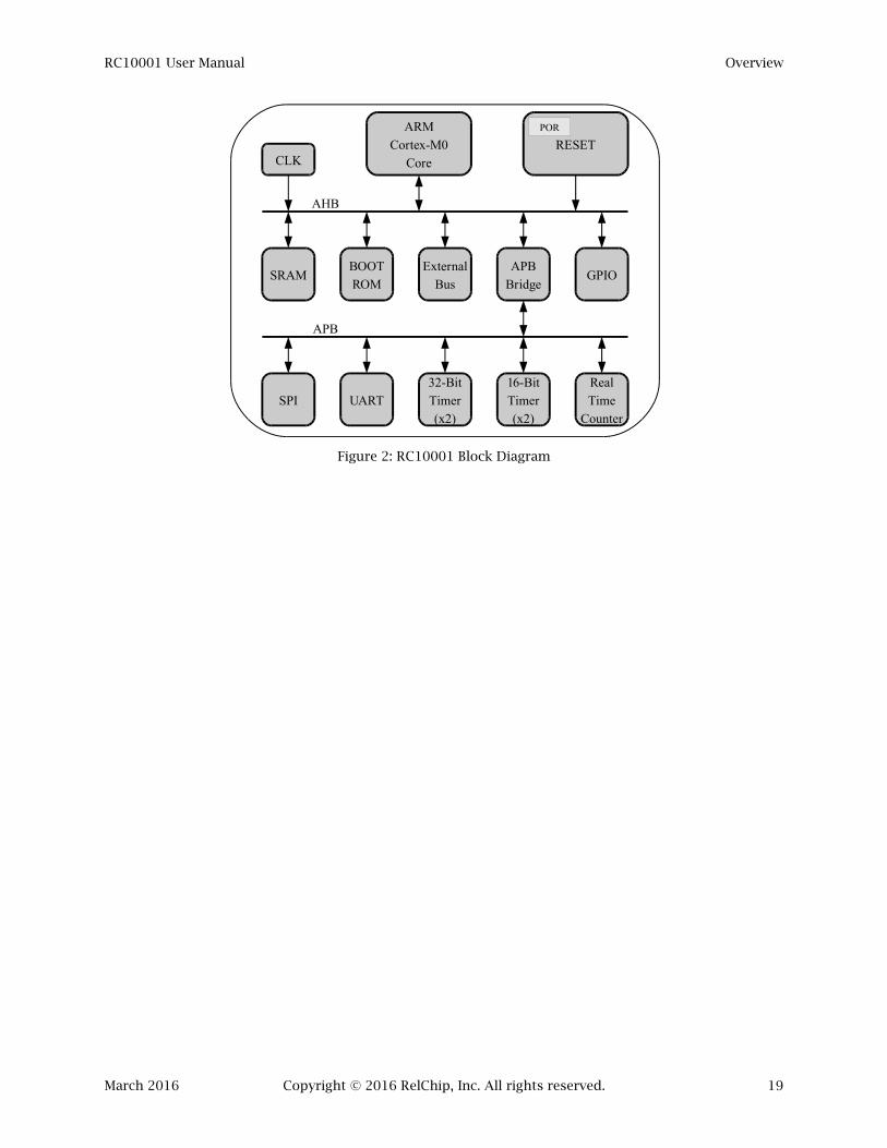
RC10001 User Manual Overview
March 2016 Copyright © 2016 RelChip, Inc. All rights reserved. 19
Figure 2: RC10001 Block Diagram
AHB
APB
CLK
ARM
Cortex-M0
Core
RESET
POR
SRAMAPB
Bridge
External
BusGPIO
BOOT
ROM
SPI
16-Bit
Timer
(x2)
32-Bit
Timer
(x2)
Real
Time
Counter
UART

RC10001 User Manual The Cortex-M0 Processor
March 2016 Copyright © 2016 RelChip, Inc. All rights reserved. 20
2 THE CORTEX-M0 PROCESSOR
The Cortex-M0 is a thirty-two bit processor core and memory bus for data while utilizing the sixteen bit Thumb-2 instruction set. Two instructions per memory location increases processing efficiency and compacts code. This section describes execution, data processing, and resources available. The Cortex-M0 Instructions section covers the instructions.
2.1 BASICS
The Cortex-M0 core is a fully static core developed by ARM® LTD. The Cortex-M0 core uses a three-stage pipeline: fetch, execute, and write-back. Thirty-two bit transfers on the bus mean one fetch is executed every two cycles (except in the rare thirty-two bit instruction case). A reads and writes from/to memory (LDR, LDM, STR, STM, PUSH, and POP instructions) take one cycle per location, independent of the size of the transfer (word, halfword, or byte). When possible, a single load or store operation will occur between fetches, removing the requirement for a second cycle to execute those instructions.
All register-to-register instructions (including multiply) take one cycle to execute, and nearly all memory access instructions take two (multiple access instructions such as push and pop take more). The cycles-per-instruction (CPI) improve due to fetching two instructions in one memory cycle. However, given a section of code at a predetermined even or odd address, the execution remains deterministic.
The processor is a little endian processor for byte, halfword and instruction ordering, and big endian when bit significance is determined. That is, a register’s most significant bit is thirty-one and the least significant is zero (reg [31:0]). However, byte address storage is little endian as Table 1 and Table 2 show. Support for byte, halfword, and word data is included in the instruction set.
Table 1: Little Endian Byte Storage
Address Byte Storage
2b00 D[7:0]
2b01 D[15:8]
2b10 D[23:16]
2b11 D[31:24]
Table 2: Little Endian Halfword & Instruction Storage
Address Halfword Storage Instruction First Byte Second Byte
2b0X D[15:0] First Instruction D[7:0] D[15:8]
2b1X D[31:16] Second Instruction D[23:16] D[31:24]
Two modes of operation are available in the RC10001, thread and handler. Thread mode is the fundamental mode that can use either the main stack pointer (MSP) or the process stack pointer (PSP). Reset selects thread mode and the main stack pointer. All exceptions execute in the handler mode, using the main stack pointer (MSP). The two modes allow separation from user code (thread mode) and operating system code (handler mode).
The stack is a full-descending stack. Pushing onto the stack requires first descending from the current stack pointer, and then storing the data. On a pop, a read occurs before incrementing the stack pointer. There is a hardware guarantee of eight-byte stack address alignment on exception entry.

RC10001 User Manual The Cortex-M0 Processor
March 2016 Copyright © 2016 RelChip, Inc. All rights reserved. 21
2.2 CORE REGISTERS
The core contains a register bank of sixteen general-purpose registers and four special purpose registers. Any instruction can access the first eight general-purpose registers (R0 to R7). All registers are thirty-two bit.
Table 3: Cortex-M0 Core Registers
General Special Description Reset
R0-R12 - General Purpose -
R13 SP Connection to PSP or MSP -
R14 LR Link -
R15 PC Program Counter @[Address[4]]
- MSP Main Stack Pointer -
- PSP Process Stack Pointer -
- PSR Program Status -
- PRIMASK Priority Mask 0x0000_0000
- CONTROL Control 0x0000_0000
2.2.1 R12/SP - Stack Pointer Register
Figure 3: Stack Pointer Registers
A: ([31:2] = PTR) Stack Pointer.
The stack pointer register is the current selected stack pointer, MSP or PSP. When operating in thread mode, the processor can use either the main stack pointer (MSP) or the process stack pointer (PSP). When in the handler mode, it uses the main stack pointer (MSP) exclusively. The stack pointer is word aligned. The reserved bits (A1 and A0) are always 0b01, indicating word addressing with Thumb instructions.
2.2.2 MSP/PSP - Stack Pointer Registers
The stack pointer register, SP, accesses the configured stack pointer, main or process. The SPSEL bit in the CONTROL register determines the stack pointer to use in thread mode. In handler mode, only the main stack pointer is used. Reset selects the main stack pointer.
31A
RW(X)
A
RW(X)
A
RW(X)
A
RW(X)
A
RW(X)
A
RW(X)
A
RW(X)
A
RW(X)
A
RW(X)
A
RW(X)
A
RW(X)
A
RW(X)
A
RW(X)
A
RW(X)
A
RW(X)
A
RW(X)
A
RW(X)
A
RW(X)
A
RW(X)
A
RW(X)
A
RW(X)
A
RW(X)
A
RW(X)
A
RW(X)
A
RW(X)
A
RW(X)
A
RW(X)
A
RW(X)
A
RW(X)
2A
RW(X)
1
R(0)
0
R(1)
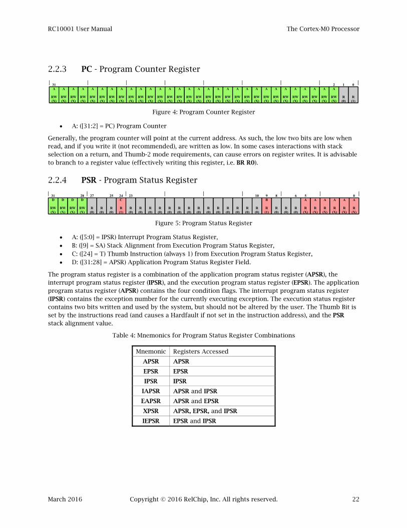
RC10001 User Manual The Cortex-M0 Processor
March 2016 Copyright © 2016 RelChip, Inc. All rights reserved. 22
2.2.3 PC - Program Counter Register
Figure 4: Program Counter Register
A: ([31:2] = PC) Program Counter
Generally, the program counter will point at the current address. As such, the low two bits are low when read, and if you write it (not recommended), are written as low. In some cases interactions with stack selection on a return, and Thumb-2 mode requirements, can cause errors on register writes. It is advisable to branch to a register value (effectively writing this register, i.e. BR R0).
2.2.4 PSR - Program Status Register
Figure 5: Program Status Register
A: ([5:0] = IPSR) Interrupt Program Status Register, B: ([9] = SA) Stack Alignment from Execution Program Status Register, C: ([24] = T) Thumb Instruction (always 1) from Execution Program Status Register, D: ([31:28] = APSR) Application Program Status Register Field.
The program status register is a combination of the application program status register (APSR), the interrupt program status register (IPSR), and the execution program status register (EPSR). The application program status register (APSR) contains the four condition flags. The interrupt program status register (IPSR) contains the exception number for the currently executing exception. The execution status register contains two bits written and used by the system, but should not be altered by the user. The Thumb Bit is set by the instructions read (and causes a Hardfault if not set in the instruction address), and the PSR stack alignment value.
Table 4: Mnemonics for Program Status Register Combinations
Mnemonic Registers Accessed
APSR APSR
EPSR EPSR
IPSR IPSR
IAPSR APSR and IPSR
EAPSR APSR and EPSR
XPSR APSR, EPSR, and IPSR
IEPSR EPSR and IPSR
31A
RW(X)
A
RW(X)
A
RW(X)
A
RW(X)
A
RW(X)
A
RW(X)
A
RW(X)
A
RW(X)
A
RW(X)
A
RW(X)
A
RW(X)
A
RW(X)
A
RW(X)
A
RW(X)
A
RW(X)
A
RW(X)
A
RW(X)
A
RW(X)
A
RW(X)
A
RW(X)
A
RW(X)
A
RW(X)
A
RW(X)
A
RW(X)
A
RW(X)
A
RW(X)
A
RW(X)
A
RW(X)
A
RW(X)
2A
RW(X)
1
R(0)
0
R(1)
31D
RW(X)
D
RW(X)
D
RW(X)
28D
RW(X)
24C
R(1)
27
R(0)
R(0)
25
R(0)
23
R(0)
R(0)
R(0)
R(0)
R(0)
R(0)
R(0)
R(0)
R(0)
R(0)
R(0)
R(0)
R(0)
10
R(0)
9B
R(1)
8
R(0)
R(0)
6
R(0)
5A
R(X)
A
R(X)
A
R(X)
A
R(X)
A
R(X)
0A
R(X)
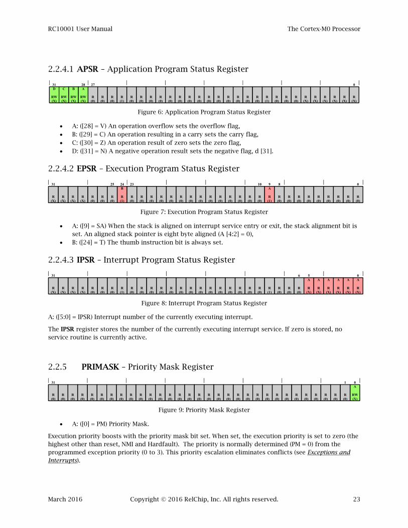
RC10001 User Manual The Cortex-M0 Processor
March 2016 Copyright © 2016 RelChip, Inc. All rights reserved. 23
2.2.4.1 APSR – Application Program Status Register
Figure 6: Application Program Status Register
A: ([28] = V) An operation overflow sets the overflow flag, B: ([29] = C) An operation resulting in a carry sets the carry flag, C: ([30] = Z) An operation result of zero sets the zero flag, D: ([31] = N) A negative operation result sets the negative flag, d [31].
2.2.4.2 EPSR – Execution Program Status Register
Figure 7: Execution Program Status Register
A: ([9] = SA) When the stack is aligned on interrupt service entry or exit, the stack alignment bit is set. An aligned stack pointer is eight byte aligned (A [4:2] = 0),
B: ([24] = T) The thumb instruction bit is always set.
2.2.4.3 IPSR – Interrupt Program Status Register
Figure 8: Interrupt Program Status Register
A: ([5:0] = IPSR) Interrupt number of the currently executing interrupt.
The IPSR register stores the number of the currently executing interrupt service. If zero is stored, no service routine is currently active.
2.2.5 PRIMASK – Priority Mask Register
Figure 9: Priority Mask Register
A: ([0] = PM) Priority Mask.
Execution priority boosts with the priority mask bit set. When set, the execution priority is set to zero (the highest other than reset, NMI and Hardfault). The priority is normally determined (PM = 0) from the programmed exception priority (0 to 3). This priority escalation eliminates conflicts (see Exceptions and Interrupts).
31D
RW(X)
C
RW(X)
B
RW(X)
28A
RW(X)
27
R(0)
R(0)
R(0)
R(0)
R(0)
R(0)
R(0)
R(0)
R(0)
R(0)
R(0)
R(0)
R(0)
R(0)
R(0)
R(0)
R(0)
R(0)
R(0)
R(0)
R(1)
R(1)
R(X)
R(X)
R(X)
R(X)
R(X)
0
R(X)
24B
R(1)
R(0)
R(0)
25
R(0)
23
R(0)
R(0)
R(0)
R(0)
R(0)
R(0)
R(0)
R(0)
R(0)
R(0)
R(0)
R(0)
R(0)
10
R(0)
9A
R(1)
8
R(0)
R(0)
R(0)
R(X)
R(X)
R(X)
31
R(X)
R(0)
R(0)
R(0)
R(0)
R(0)
0
R(0)
R(0)
R(0)
R(0)
R(0)
R(0)
R(0)
R(0)
R(0)
R(0)
R(0)
R(0)
R(0)
R(0)
R(0)
R(0)
R(0)
R(0)
R(0)
R(0)
6
R(0)
5A
R(X)
A
R(X)
A
R(X)
A
R(X)
A
R(X)
0A
R(X)
R(X)
R(X)
R(X)
31
R(X)
R(1)
R(1)
0A
RW(X)
R(0)
R(0)
R(0)
R(0)
R(0)
R(0)
R(0)
R(0)
R(0)
R(0)
R(0)
R(0)
R(0)
R(0)
R(0)
R(0)
R(0)
R(0)
R(0)
R(0)
R(0)
R(0)
R(0)
31
R(0)
R(0)
R(0)
R(0)
R(0)
R(0)
R(0)
1
R(0)

RC10001 User Manual The Cortex-M0 Processor
March 2016 Copyright © 2016 RelChip, Inc. All rights reserved. 24
2.2.6 CONTROL - Control Register
Figure 10: Control Register
A: ([1] = SPSEL) Stack pointer select.
When in thread mode, the SPSEL bit is writable. When set, the PSP is the stack pointer in thread mode. The main stack pointer (MSP) is the stack pointer for the handler mode.
Any write to the control register is followed by the ISB instruction to insure the result takes effect before the next instruction is executed.
1A
RW(X)
R(0)
R(0)
R(0)
R(0)
R(0)
R(0)
R(0)
R(0)
R(0)
R(0)
R(0)
R(0)
R(0)
R(0)
R(0)
R(0)
R(0)
R(0)
R(0)
R(0)
R(0)
R(0)
R(0)
31
R(0)
R(0)
R(0)
R(0)
R(0)
R(0)
2
R(0)
0
R(0)
RC10001 User Manual Exceptions and Interrupts
March 2016 Copyright © 2016 RelChip, Inc. All rights reserved. 25
3 EXCEPTIONS AND INTERRUPTS
An exception or interrupt is an anomalous event that changes the normal execution flow of a program. The initiator of an interrupt or exception can be internal or external, synchronous or asynchronous. For example, an illegal instruction generates a Hardfault internally. UART data reception (external source) can generate an interrupt. Another alternative is execution of the service interrupts, initiated by code.
Any exception will be in one of four states.
Inactive: Exception is currently not active or pending. Pending: Exception has triggered, but not serviced. This occurs whenever exceptions of the same
or higher priority are active. Active: Exception service currently. Active and Pending: Exception service currently and another of the same exception type is waiting.
Exceptions processing occurs in priority order. Chaining occurs for subsequent exceptions of the same priority or lower. The processor operates on the highest priority first. Table 5 lists possible priorities.
Exceptions use the stack, eight-byte aligned, to store the current stack pointer. Alignment appears in the execution program status register, EPSR.

RC10001 User Manual Exceptions and Interrupts
March 2016 Copyright © 2016 RelChip, Inc. All rights reserved. 26
Table 5: Interrupts
Exception Name Priority
Reset Reset -3
NMI Non-Maskable Interrupt -2
Hardfault Hardfault -1
SVCall System Service Call 0-3
DebugMonitor Debug Monitor 0-3
SysTick System Tick Timer 0-3
WAKEUP Wake Up 0-3
RAM RAM Parity 0-3
TIM16A 16 bit Timer A 0-3
TIM16B 16 bit Timer B 0-3
TIM32A 32 bit Timer A 0-3
TIM32B 32 bit Timer B 0-3
SSP Synchronous Serial Interface 0-3
UART UART 0-3
WDT Watchdog Timer 0-3
SVC1 Service 0-3
GPIO0 General Purpose IO 0 0-3
GPIO1 General Purpose IO 1 0-3
GPIO2 General Purpose IO 2 0-3
GPIO3 General Purpose IO 3 0-3
GPIO4 General Purpose IO 4 0-3
GPIO5 General Purpose IO 5 0-3
GPIO6 General Purpose IO 6 0-3
GPIO7 General Purpose IO 7 0-3
RTC Real Time Clock 0-3
SVC2 Service 0-3
EINT External Bus 0-3
- Normal Execution 4
RC10001 User Manual Exceptions and Interrupts
March 2016 Copyright © 2016 RelChip, Inc. All rights reserved. 27
3.1 PRIORITY
The Nested Vector Interrupt Controller (NVIC) uses the fixed priority of the reset exception, the non-maskable interrupt, and the Hardfault exception to supersede any other interrupts (Table 5). The remaining interrupts have a programmable priority of 0 to 3 (0 being highest priority). The NVIC selects the highest priority exception to execute. If two interrupts compete for execution at the same priority level, the lowest number interrupt will execute first.
Interrupts chain through the NVIC. When an interrupt completes and another interrupt is pending, control transfers to the next interrupt using the frame from the previous interrupt, shortcutting pop and push cycles. ISR – Interrupt Service Routine Entry and Exit describes chaining.
3.1.1 Reset
A reset exception, taken from any source in the RC10001, is the highest priority exception. It restarts the part with the MSP loaded from the contents of memory location 0, and the first address to execute from memory location 4 (PC <= RAM [4]). This exception resets state.
If the reset source is an external HARDRESETn, or caused by a power on sequence (power-on-reset or POR), the memory will be loaded with the appropriate boot source (see Reset and Boot Methods) prior to starting execution.
3.1.2 Non-Maskable Interrupt (NMI)
The non-maskable interrupt triggers by a specific register write.
3.1.3 Hardfault
A number of error conditions trigger the Hardfault exception. Error conditions causing a Hardfault exception are:
Instruction Execution Errors. Illegal Opcode or Operation. Undefined Instruction. Illegal Memory Access (such as writing a read-only address segment). Alignment Errors.
o Not Word Aligned for LDM, LDR, POP, PUSH, STM, or STR. o Not Halfword Aligned for LDRH and STRH.
Exception Entry with Address [0] set low (non-Thumb). Load an Unaligned Value for the Stack into the Program Counter during an Exception Return. BLX, BX, and POP Instructions to the PC Produces an Invalid Execution State if Bit [0] is low.
Executing Another Instruction while in an Invalid Execution State causes a Hardfault or Lockup.
A Hardfault that occurs during a Hardfault exception will cause the system to lockup. Only the debug interface or a reset can restore processor operation from a lockup state.

RC10001 User Manual Exceptions and Interrupts
March 2016 Copyright © 2016 RelChip, Inc. All rights reserved. 28
3.1.4 Supervisor Call
Four interrupts/exceptions make supervisor calls, allowing multiple priorities. SVCall, PendSV, SVC1, and SVC2 access system software from the applications. An immediate operating system call executes from a SVCall. PendSV creates a lower priority “pending” service call. The remaining two service calls create low priority service calls by writing the NVIC_IPSR register.
Occasionally, a service call might remain in a pending state because other exceptions are higher priority. The PRIMASK register boosts the priority to the highest (except for Reset, NMI, and Hardfault) priority interrupt, insuring progress.
3.1.5 Debug Monitor
The debug monitor exception is not available in the RC10001.
3.1.6 SysTick – System Tick Timer
When set and enabled, the SysTick can provided periodic interrupts. This schedules repetitive activities such as operating system schedulers, and periodic sampling in simple systems.
3.1.7 Peripheral Interrupts
Each individual peripheral block configures its interrupts (see Table 5). The peripheral block and the NVIC combine to enable an interrupt. Likewise, both levels clear the interrupts.
Two special peripheral interrupts, SVC1 and SVC2, are additional software interrupts. The NVIC level enable and pending bits are set. The interrupt service routine will clear these before exit. There are no hardware generated interrupts for SVC1 and SVC2.
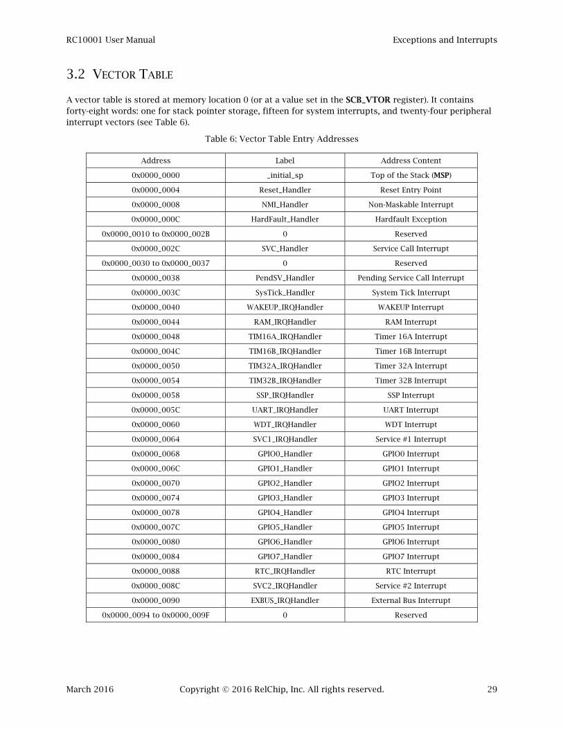
RC10001 User Manual Exceptions and Interrupts
March 2016 Copyright © 2016 RelChip, Inc. All rights reserved. 29
3.2 VECTOR TABLE
A vector table is stored at memory location 0 (or at a value set in the SCB_VTOR register). It contains forty-eight words: one for stack pointer storage, fifteen for system interrupts, and twenty-four peripheral interrupt vectors (see Table 6).
Table 6: Vector Table Entry Addresses
Address Label Address Content
0x0000_0000 _initial_sp Top of the Stack (MSP)
0x0000_0004 Reset_Handler Reset Entry Point
0x0000_0008 NMI_Handler Non-Maskable Interrupt
0x0000_000C HardFault_Handler Hardfault Exception
0x0000_0010 to 0x0000_002B 0 Reserved
0x0000_002C SVC_Handler Service Call Interrupt
0x0000_0030 to 0x0000_0037 0 Reserved
0x0000_0038 PendSV_Handler Pending Service Call Interrupt
0x0000_003C SysTick_Handler System Tick Interrupt
0x0000_0040 WAKEUP_IRQHandler WAKEUP Interrupt
0x0000_0044 RAM_IRQHandler RAM Interrupt
0x0000_0048 TIM16A_IRQHandler Timer 16A Interrupt
0x0000_004C TIM16B_IRQHandler Timer 16B Interrupt
0x0000_0050 TIM32A_IRQHandler Timer 32A Interrupt
0x0000_0054 TIM32B_IRQHandler Timer 32B Interrupt
0x0000_0058 SSP_IRQHandler SSP Interrupt
0x0000_005C UART_IRQHandler UART Interrupt
0x0000_0060 WDT_IRQHandler WDT Interrupt
0x0000_0064 SVC1_IRQHandler Service #1 Interrupt
0x0000_0068 GPIO0_Handler GPIO0 Interrupt
0x0000_006C GPIO1_Handler GPIO1 Interrupt
0x0000_0070 GPIO2_Handler GPIO2 Interrupt
0x0000_0074 GPIO3_Handler GPIO3 Interrupt
0x0000_0078 GPIO4_Handler GPIO4 Interrupt
0x0000_007C GPIO5_Handler GPIO5 Interrupt
0x0000_0080 GPIO6_Handler GPIO6 Interrupt
0x0000_0084 GPIO7_Handler GPIO7 Interrupt
0x0000_0088 RTC_IRQHandler RTC Interrupt
0x0000_008C SVC2_IRQHandler Service #2 Interrupt
0x0000_0090 EXBUS_IRQHandler External Bus Interrupt
0x0000_0094 to 0x0000_009F 0 Reserved
RC10001 User Manual Exceptions and Interrupts
March 2016 Copyright © 2016 RelChip, Inc. All rights reserved. 30
3.3 WFE/WFI – WAIT FOR EVENT, WAIT FOR INTERRUPT
Program execution halts with the WFE and WFI instructions. They suspend operation until encountering a specific event or interrupt. These instructions power up from sleep states, or simply wait for an interrupt.
WFE waits for the following events:
A reset. Any exception entering the pending state with the SEVONPEND bit in the System Control Register
set (see SCB_SCR - System Control Register). An asynchronous exception at a priority that preempts any currently active exceptions. A debug event with debug enabled (see DCB_DHCSR - Debug Halting Control and Status Register).
Executing WFE resets the event register. Before using it to wait for an event, read the register to clear it.
WFI waits for the following events:
A reset. If the PM bit of PRIMASK register is set low, any exception that would preempt any currently
active exception. If the PM bit is set high, the exception must have a higher group priority than the current exception level to exit.
A debug event with debug enabled (see DCB_DHCSR - Debug Halting Control and Status Register).
3.4 ISR – INTERRUPT SERVICE ROUTINE ENTRY AND EXIT
Exceptions and interrupts have an associated priority level (see Table 5) which may or may not be programmable. The priority of the executing instruction stream is defined as the execution priority, while a group of exceptions with the same priority is defined as the priority group.
Setting the PRIMASK register bit raises the execution priority to “0”. This prevents any exceptions with configurable priority from activating unless the fault escalation mechanism is used. When the group priority of the SVCall is lower than or equal to the currently executing group priority, inhibiting normal preemption, a Hardfault exception asserts.
3.4.1 Reset Entry Special Considerations
The reset exception resets registers in the RC10001, sets the stack pointer from the vector table, and branches to the location stored in the vector table. It does not reset the persistent flags in the Serial Wire Debug Unit.
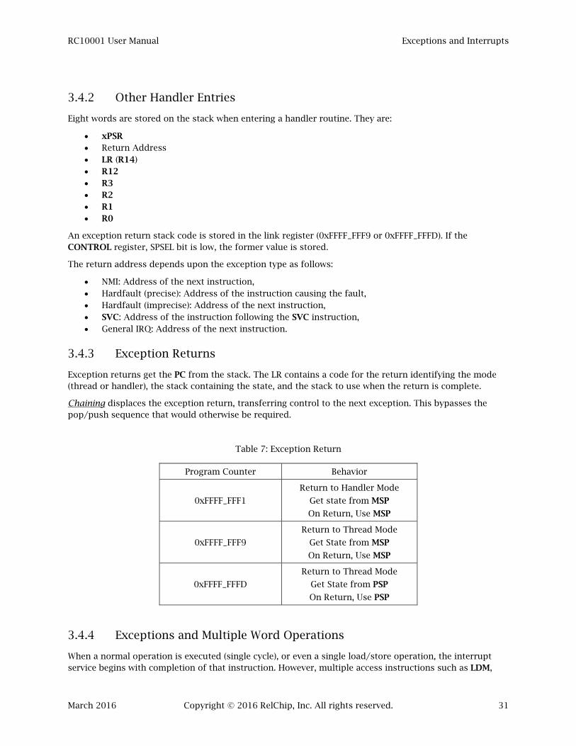
RC10001 User Manual Exceptions and Interrupts
March 2016 Copyright © 2016 RelChip, Inc. All rights reserved. 31
3.4.2 Other Handler Entries
Eight words are stored on the stack when entering a handler routine. They are:
xPSR Return Address LR (R14) R12 R3 R2 R1 R0
An exception return stack code is stored in the link register (0xFFFF_FFF9 or 0xFFFF_FFFD). If the CONTROL register, SPSEL bit is low, the former value is stored.
The return address depends upon the exception type as follows:
NMI: Address of the next instruction, Hardfault (precise): Address of the instruction causing the fault, Hardfault (imprecise): Address of the next instruction, SVC: Address of the instruction following the SVC instruction, General IRQ: Address of the next instruction.
3.4.3 Exception Returns
Exception returns get the PC from the stack. The LR contains a code for the return identifying the mode (thread or handler), the stack containing the state, and the stack to use when the return is complete.
Chaining displaces the exception return, transferring control to the next exception. This bypasses the pop/push sequence that would otherwise be required.
Table 7: Exception Return
Program Counter Behavior
0xFFFF_FFF1
Return to Handler Mode
Get state from MSP
On Return, Use MSP
0xFFFF_FFF9
Return to Thread Mode
Get State from MSP
On Return, Use MSP
0xFFFF_FFFD
Return to Thread Mode
Get State from PSP
On Return, Use PSP
3.4.4 Exceptions and Multiple Word Operations
When a normal operation is executed (single cycle), or even a single load/store operation, the interrupt service begins with completion of that instruction. However, multiple access instructions such as LDM,
RC10001 User Manual Exceptions and Interrupts
March 2016 Copyright © 2016 RelChip, Inc. All rights reserved. 32
STM, PUSH, and POP will interrupt immediately, and re-execute the instruction for all multiple locations after the interrupt routine. Stack pointer update occurs last, avoiding corruption. Multiple access instructions can cause incorrect data storage to/from peripherals.
3.4.5 Chaining
Tail chaining of exceptions bypasses the pop/return sequence of the current exception, and the entry/push operation of the next one.
When no exceptions are left pending, the exception return occurs, and normal execution resumes.
RC10001 User Manual Memory
March 2016 Copyright © 2016 RelChip, Inc. All rights reserved. 33
4 MEMORY
4.1 MEMORY TYPES
The three types of memory are normal (weakly ordered), device, and strongly ordered. Normal memory includes all memory where reading or writing does not cause side effects. Peripherals are device memory, or in some cases, strongly ordered memory. Strongly ordered memory may cause side effects some cycles after a write occurs. The user is responsible for possible side effects in strongly ordered memory writes. The RC10001 orders operations on the bus, but cannot account for deferred activities external to the controller. The use of external read/write operations is never restricted in memory operations, and can be problematic whenever a peripheral write causes side effects.
Memory access, either fetch or data read/write, will occur in sequence in the RC10001. Fetch and data memory accesses are sequenced on the single thirty-two bit internal bus (the AHB bus), and kept in proper order A pre-fetched instruction will be discarded upon branching (no branch prediction).
Device memory for peripherals may have side effects. Consider the case of an exception generation during a STM (Store Multiple) operation to a FIFO. When the exception handler returns, the STM will start at the first transfer, polluting the FIFO.
When side effects of a write may occur some cycles later, the memory is strongly ordered. Code can conceivable change the processor state, but have subsequent code execute before the change is complete. Writing the CONTROL register to select the stack during an exception may cause the storage on the wrong stack. Good practice uses the ISB instruction immediately following strongly ordered writes.
Avoid multiple memory or peripheral read/write instructions (LDM, STM, PUSH, and POP) when accessing device or strongly ordered memory. Instruction fetches can only access normal memory. A fetch from device or strongly ordered memory causes a hardfault.
4.2 MEMORY REGIONS
There are eight segments of the RC10001 address space. Eight 0.5GB regions in the 4GB memory space are:
Code SRAM Peripheral Two RAM Segments Two Device Segments System
4.2.1 Code Region
The code region (internal reserved) exists from address 0x0000_0000 to address 0x1FFF_FFFF. This region contains the internal boot ROM and RAM. In the RC10001, code, read-only data, and read-write data reside in the RAM. The vector table (reset routine addresses) resides at location 0x00000000.

RC10001 User Manual Memory
March 2016 Copyright © 2016 RelChip, Inc. All rights reserved. 34
4.2.2 SRAM Region
The SRAM region is not supported.
4.2.3 Peripheral Region
Internal peripherals are located in this address space. Some of these devices are strongly ordered. Using multiple transaction commands (LDM, STM) can cause problems.
4.2.4 RAM Segments (2)
These are external RAM memory segments, used for code and/or data.
4.2.5 Device Segments (2)
These are external peripheral device segments. This area is strongly ordered. Attempts to fetch instructions from this area will cause a hardfault. Using multiple transaction commands (LDM, STM) can cause problems.
4.2.6 System Region
The Private Peripheral Bus (PPB) occupies the first half of the system region. The RelChip system registers occupy the second half. The PPB contains key system resources such as the System Control Space (SCS), and the debug unit.
All accesses to the PPB region are strongly ordered. Generating an exception while executing a write to this region, can cause corruption or worse. Thus, the use of multiple access instructions, LDM and STM, in this region is prohibited. Strongly ordered memory should only be word accessed. Any access that crosses a memory attribute border produces unpredictable results.
Note that any access that crosses a strongly ordered memory boundary, or any other attribute boundary, yields unpredictable results.
4.2.7 Memory and Instruction Barrier Instructions
The memory barrier instructions, DMB and DSB, and the instruction barrier instruction, ISB, correct system synchronization.
The data memory barrier instruction, DMB, in the program flow prevents the processor from accessing memory until all previous memory accesses are complete. This insures memory consistency before another access, in particular with strongly ordered memory.
The data synchronization barrier instruction, DSB, prevents the processor to execute an instruction until all previous memory accesses are complete. This is useful to insure peripheral and control writes are complete.
The instruction synchronization barrier, ISB, flushes the processor pipeline before refilling and executing further instructions. A solid processor state is insured.

RC10001 User Manual Memory
March 2016 Copyright © 2016 RelChip, Inc. All rights reserved. 35
Internal 0xFFFF_FFFF
Reserved 0xE010_0000
0xE00F_FFFF 0xE00F_FFFF
ROM Table 0xE00F_F000
Reserved 0xE000_F000
Internal System Control Space 0xE000_E000
Private Peripheral Bus Reserved 0xE000_3000
Breakpoint Unit 0xE000_2000
Data Watchpoint Unit 0xE000_1000
0xE000_0000 Reserved 0xE000_0000
External 0xDFFF_FFFF
Device/Storage 0xA000_0000
External 0x9FFF_FFFF
Code/Storage 0x6000_0000
Internal 0x5FFF_FFFF
Reserved 0x5008_0000
0x5007_FFFF 0x5007_FFFF
GPIO 7 0x5000_7000
GPIO 6 0x5000_6000
GPIO 5 0x5000_5000
Internal GPIO 4 0x5000_4000
AHB Peripherals GPIO 3 0x5000_3000
GPIO 2 0x5000_2000
GPIO 1 0x5000_1000
0x5000_0000 GPIO 0 0x5000_0000
Internal 0x4FFF_FFFF
Reserved 0x4008_0000
0x4007_FFFF 0x4007_FFFF
Reserved 0x4004_C000
System Control 0x4004_8000
IOCONFIG 0x4004_4000
SSP 0x4004_0000
Reserved 0x4002_C000
EXBUS Configuration 0x4002_8000
Internal Reserved 0x4002_4000
APB Peripherals RAM Configuration 0x4002_0000
Real Time Clock (RTC) 0x4001_C000
32-Bit TIMER32B 0x4001_8000
32-Bit TIMER32A 0x4001_4000
16-Bit TIMER16B 0x4001_0000
16-Bit TIMER16A 0x4000_C000
UART 0x4000_8000
Watchdog Timer (WDT) 0x4000_4000
0x4000_0000 Reserved 0x4000_0000
External 0x3FFF_FFFF
Code/Data 0x1000_0000
Internal 0x0FFF_FFFF
Reserved 0x0000_1400
Internal 0x0000_23FF
Boot ROM 0x0000_2000
Internal 0x0000_0FFF
4KB SRAM 0x0000_0000
Figure 11: Memory Map

RC10001 User Manual Power Management
March 2016 Copyright © 2016 RelChip, Inc. All rights reserved. 36
5 POWER MANAGEMENT
Both sleep modes and clock domain enables lower power requirements. Two sleep modes exist in the Cortex-M0. Sleep modes stop microcontroller activity including instruction execution. Peripheral clock enables select which circuits consume power.
5.1 CORTEX-M0 CORE SLEEP MODES
The Cortex-M0 core includes two sleep modes, sleep and deep sleep. The SLEEPDEEP bit of the SCB_SCR - System Control Register selects the mode. This register controls sleep mode reentry on service routine exit.
5.1.1 Sleep Mode
Sleep mode stops processor execution, not the clock or the peripheral clocks. This mode allows peripherals to continue to operate independently (such as transmitting or receiving on the UART). It also allows signals on the peripherals to “wake up” the processor via previously enabled interrupts.
5.1.2 Deep Sleep Mode
Deep sleep mode stops both the processor and peripherals Note that stopping the peripheral clocks (deep sleep) will prevent peripheral interrupts waking the part. The WAKEUP pin bypasses this restriction, allowing an external signal to “wake up” the part asynchronously.
5.1.3 Wait for Interrupt Wake Up-WFI
This instruction causes to processor to enter the appropriate sleep mode (SCB_SCR - System Control Register). The processor will wake up on reset, an interrupt, or a debugger event as configured. Note that stopping peripheral clocks (deep sleep) will prevent peripheral interrupts.
5.1.4 Wait for Event Wake Up-WFE
The WFE instruction causes the processor to enter the appropriate sleep mode (SCB_SCR - System Control Register), and wait until the event register is one. Reset, wakeup interrupt, or the debugger set the event register. Note that stopping peripheral clocks (deep sleep) will prevent peripheral interrupts.
5.1.5 Sleep on Exception Exit
If the SLEEPONEXIT bit is set in the SCB_SCR - System Control Register, the processor will sleep mode when interrupt service routines exit.
RC10001 User Manual Power Management
March 2016 Copyright © 2016 RelChip, Inc. All rights reserved. 37
5.1.6 Deferred Exit from Sleep Mode
When it is desirable to not immediately interrupt when exiting sleep mode (external power up times may require this), programming the PRIMASK – Priority Mask Register PM bit to one escalates the current execution priority such that the interrupt will not be serviced until the bit is cleared.
5.1.7 “C” Functions
Standard “C” functions access assembly instructions. They are located in the header files that should be included with your development system. The functions are:
void __disable_irq(void) // Assembly CPSID Equivalent void __enable_irq(void)) // Assembly CPSIE Equivalent void __NOP(void) // Assembly NOP Equivalent void __DMB(void) // Assembly DMB Equivalent void __DSB(void) // Assembly DSB Equivalent void __ISB(void) // Assembly ISB Equivalent uint32_t __REV(uint32_t value) // Assembly REV Equivalent uint32_t __REV16(uint32_t value) // Assembly REV16 Equivalent int32_t __REVSH(int32_t value) // Assembly REVSH Equivalent uint32_t __ROR(uint32_t op1,uint32_t op2) // Assembly ROR Equivalent void __SEV(void) // Assembly SEV Equivalent void __WFE(void) // Assembly WFE Equivalent void __WFI(void) // Assembly WFI Equivalent
5.2 PERIPHERAL CLOCK ENABLE
The SYSCON_AHBCLKCTRL - Clock Enable Register enables the peripheral clock domains. Disabling unused clocks can provide a significant power savings. Note that a peripheral with a disabled clock will still maintain all register values, and are readable. Disabling the clock disables further writes into a FIFO, and prevents removing values.
5.3 BATTERY BACKUP
The battery backup power supply maintains RAM contents and state.

RC10001 User Manual Reset and Boot Methods
March 2016 Copyright © 2016 RelChip, Inc. All rights reserved. 38
6 RESET AND BOOT METHODS
There are two basic reset options, hard and soft. A soft reset resets the basic system state and begins execution at the vector table address. A hard reset boots the program and then performs a soft reset. Power application (POR), HARDRESETn, or a soft reset without valid RAM data cause a hard reset.
The SSP interface, UART interface, external bus, or serial wire debug interface are optional boot sources. BOOT_SEL0 and BOOT_SEL1 select the source (see Table 8).
Table 8: Boot Options
BOOT_SEL1 BOOT_SEL0 Boot Source
0 0 SSP Interface
0 1 UART Interface
1 0 External Bus
1 1 Serial Wire Debug
6.1 RESET OPTIONS AND SOURCES
There are seven potential triggers, or sources, for a reset. These are power-on reset, hard reset, soft reset, watchdog timer, battery backup, system software, and the debugger. The source of the last reset is held in the SYSCON_RSTSTAT register (all except the debugger reset).
6.1.1 Power-On Reset (POR)
When first powered, an internal circuit triggers that will issue a reset, wait for clock stability, and then boot with the code in the boot ROM. Approximately 8 milliseconds after the clock starts (at 8 MHz), the RC10001 will exit the reset and begin operating in a hard reset sequence (registers reset, boot the code, and begin the program).
Asserting (low) the HARDRESETn pin bypasses the power-on reset delay.
6.1.2 Hard Reset (HARDRESETn)
A low signal on the external HARDRESETn pin will disable the POR counter and issue a hard reset. When the HARDRESETn pin transitions high, the boot ROM executes. Once the boot ROM completes, the microcontroller will reset using the loaded vector table and code.

RC10001 User Manual Reset and Boot Methods
March 2016 Copyright © 2016 RelChip, Inc. All rights reserved. 39
6.1.3 Soft Reset (SOFTRESETn)
Asserting the SOFTRESETn pin initiates a soft reset. The microcontroller state resets and execution begins with the vector table address. The RAM does not require boot loading.
6.1.4 Watchdog Timer Reset (WDT)
A timeout of the watchdog timer resets the part when enabled. The microcontroller state resets and execution begins with the vector table address. The RAM does not require boot loading.
6.1.5 Battery Backup Reset
If battery backup is enabled (SYSCON_BATTCTRL), and the main power goes down, a soft reset occurs when the main power is restored. This also sets a bit in the SYSCON_BOOTCTRL register.
6.1.6 System Software Reset
A system software reset is a soft reset generated by writing the SYSRESETREQ bit in the SCB_AIRCR - Application Interrupt and Reset Control Register. This may not have immediate effect. After writing SCB_AIRCR, the code should include the following:
DSB
Loop B Loop
6.1.7 Debug Reset
The serial wire debug interface generates a software soft reset with appropriate register writes.
6.2 BOOT SOURCES AND FILES
Booting is the process of loading code into the RAM, internal and external, before execution. The RC10001 boots from any of four devices, using code particularly formatted for the internal boot ROM code.
6.2.1 Boot Files and Records
The RC10001 uses a simple binary format (compatible with Keil development software) as input to the processor. This format consists of one to N packets terminated by a block of size 0. Each block consists of:
1. For UART BOOT ONLY, one byte of 0x40 is transmitted first to do auto-baud detection, 2. Size of data to store (one 32-bit unsigned integer, value = m, stored little endian); 3. Address to start loading (one 32-bit unsigned integer, stored little endian); 4. Data to Store (m 32-bit unsigned integers, stored little endian); 5. CRC 16 CCITT (one 32-bit unsigned integer packed as).
a. Byte 0 – CRC[15:8] b. Byte 1 – CRC[7:0] c. Byte 2 – 0x00 d. Byte 3 – 0x00 e. Note that RAM addresses must be mapped to begin at 0x2000 (not in the code references,
just in the packets) due to the RAM remap during boot.

RC10001 User Manual Reset and Boot Methods
March 2016 Copyright © 2016 RelChip, Inc. All rights reserved. 40
6.2.2 Common Boot ROM Process
All boot code is common except step 4 below. Step 4 follows one of 6.2.3 through 6.2.6.
1. Set SYSCON_BOOTCTRL MAP to ROM @ Address 0 2. Read Initial Stack Pointer and Program Counter from ROM 3. Read BOOT_SEL1 and BOOT_SEL0 4. Run Appropriate Boot Routine in ROM 5. Set BOOTED bit in SYSCON_BOOTCTRL 6. Remap SYSCON_BOOTCTRL MAP to RAM @ Address 0 7. Read Initial Stack Pointer and Program Counter from RAM
6.2.3 SSP Interface Boot
The SSP boot interface is configured as a master 8-bit SPI with CPOL=0, CPHA=0, and the pre-scale counter SCR = 2. The beginning of a command packet asserts SSELA. SSELA holds low until the command completes (1 to n bytes). This configuration is consistent with the defaults for RelChip RAM and ROM, as well as a Honeywell EEROM. In detail, the ROM algorithm is:
1. Configure the SSP interface with slave select 0 active as a GPIO pin (all boot devices use slave select 0),
2. Configure the SSP memory (external) to sequential mode (command 0x01 followed by 0x40); 3. Write the Address (0 is the first one), 4. Loop to read and store all the code, 5. Reset the SSP interface.
6.2.4 UART Interface Boot
The UART boot interface does auto-baud detection with a byte length of 8, 1 stop bit, and no parity. No flow control and UART speed up to 230,400 baud is supported. On completion, it simply receives the boot data until complete, and then resets itself. The steps are:
1. Configure the UART as a receiver without flow control and the TIMER 32A for auto-baud detect, 2. Receive a single byte of 0x40, 3. Detect BAUD, and configure UART for 8 bits, 1 stop, and no parity, 4. Receive and store data packets (boot), 5. Reset the UART and TIMER.
6.2.5 External Bus Boot
The external bus provides a fast parallel boot operation. The bus will use chip select 0 to enable the external device, variable latency, and x36 mode. The full 32-bit bus contains boot code. When complete, the bus will return to the GPIO configuration. The process is:
1. Configure the external bus; 2. Turn on CS 0; 3. Receive and store data packets (boot); 4. Reset the external bus to GPIO.

RC10001 User Manual Reset and Boot Methods
March 2016 Copyright © 2016 RelChip, Inc. All rights reserved. 41
6.2.6 Serial Wire Debug Boot
The serial wire debug boot is a slave to the debugging system. Internal to the boot ROM, a read of register 0 repeats until the register contains 0xA5 as set by the serial wire debug interface. When the debugger sets the terminal flag (0xA5) into R0, the boot ROM will complete.

RC10001 User Manual The Cortex-M0 Instructions
March 2016 Copyright © 2016 RelChip, Inc. All rights reserved. 42
7 THE CORTEX-M0 INSTRUCTIONS
The Thumb-2 instructions are nearly all sixteen bits wide. Very few are thirty-two bit. All can be intermixed freely. All instructions are address aligned to the halfword boundary. They are store little endian in the thirty-two bit word (see Table 2).
7.1 CONDITION FLAGS
The RC10001 supports the negative (N), zero (Z), carry (C), and overflow (V) condition flags. Generally, instructions that set the condition flags use an “S” suffix. For example, the addition (ADD) instruction does not set the condition codes, but the addition with condition codes (ADDS) does. The assembly instructions should be examined carefully for the use and setting of condition codes.

RC10001 User Manual The Cortex-M0 Instructions
March 2016 Copyright © 2016 RelChip, Inc. All rights reserved. 43
7.2 ALPHABETICAL LIST
Table 9: Instruction Set
Instruction Operand Usage Function Flags Set
ADCS {Rd,} Rd, Rm Add with Carry Rd + Rm + C -> Rd N, Z, C, V
ADD Rd, Rm Add Registers Rd + Rm -> Rd none
ADD Rd, SP, #i8 Add Immediate and SP SP + #i8 -> Rd none
ADD Rd, SP, Rd Add SP to Register SP + Rd -> Rd none
ADD Rd, SP Add SP to Register SP + Rd -> Rd none
ADD SP, Rm Add Register to SP SP + Rm -> SP none
ADD SP, #i7 Add Immediate to SP SP + #i7 -> SP none
ADD SP, SP, #i7 Add Immediate to SP SP + #i7 -> SP none
ADDS Rd, Rn, Rm Add Registers Rm + Rn -> Rd N, Z, C, V
ADDS Rdn, Rm Add Registers Rm + Rdn -> Rdn N, Z, C, V
ADDS Rd, #i8 Add Immediate to Register Rd + #i8 -> Rd N, Z, C, V
ADDS Rd ,Rn, #i3 Add Immediate to Register Rn + #i3 -> Rd N, Z, C, V
ADR Rd, #lab8 Add Immediate to PC PC + #lab8 -> Rd none
ANDS Rd, Rm Bitwise AND Rd & Rm -> Rd N, Z
ASRS Rd, Rm, #i5 Arithmetic Shift Right Imm. Rm >> #i5 -> Rd N, Z, C
ASRS Rd, Rm Arithmetic Shift Right Register Rd >> Rm -> Rd N, Z, C
B #lab11 Branch-Unconditional Go to PC + lab11 none
B[c] #lab8 Branch-Conditional If true, go to PC + lab8 none
BICS Rd, Rm Bitwise AND with Complement Rd & (!Rm) -> Rd N, Z, C
BKPT #i8 Breakpoint Break none
BL #lab25 Branch with Link PC+2->LR;
PC + #lab25->PC none

RC10001 User Manual The Cortex-M0 Instructions
March 2016 Copyright © 2016 RelChip, Inc. All rights reserved. 44
Table 10: Instruction Set Continued
Instruction Operand Usage Function Flags Set
BLX Rm Branch with Link and Exchange PC+2->LR; Rm->PC none
BX Rm Branch with Exchange Rm->PC none
CMN Rn, Rm Compare Negative Rn & (!Rm) -> Flags N, Z, C, V
CMP Rm, #i8 Compare Immediate Rn & #i8 -> Flags N, Z, C, V
CMP Rn, Rm Compare Register Rn & Rm -> Flags N, Z, C, V
CPSID Disable PRIMASK Interrupt none
CPSIE Enable PRIMASK Interrupt none
DMB Data Memory Barrier none
DSB Data Sync Barrier none
EORS Rd, Rm Bitwise Exclusive OR Registers Rd ^ Rm -> Rd N, Z
ISB Instruction Sync Barrier none
LDM Rn!, regList Load Multiple with Write back none
LDM Rn, regList Load Multiple without Write back none
LDMFD Load Multiple Full Descending none
LDMIA Load Multiple Increment After none
LDR Rt, [Rn {,#i5}] Load Word @[Rn + #i5] -> Rt none
LDR Rt, [SP {,#i8}] Load Word @[SP + #i8] -> Rt none
LDR Rt, =label Load Word label@[PC + off] -> Rt none
LDR Rt, [Rn, Rm] Load Word @[Rn + Rm] -> Rt none
LDRB Rt, [Rn {,#i5}] Load Unsigned Byte @[Rn + #i5] -> Rt none
LDRB Rt, [Rn, Rm] Load Unsigned Byte @[Rn + Rm] -> Rt none
LDRH Rt, [Rn {,#i5}] Load Unsigned Halfword @[Rn + #i5] -> Rt none
LDRH Rt, [Rn, Rm] Load Unsigned Halfword @[Rn + Rm] -> Rt none
LDRSB Rt, [Rn, Rm] Load Signed Byte @[Rn + Rm] -> Rt none
LDRSH Rt, [Rn, Rm] Load Signed Halfword @[Rn + Rm] -> Rt none
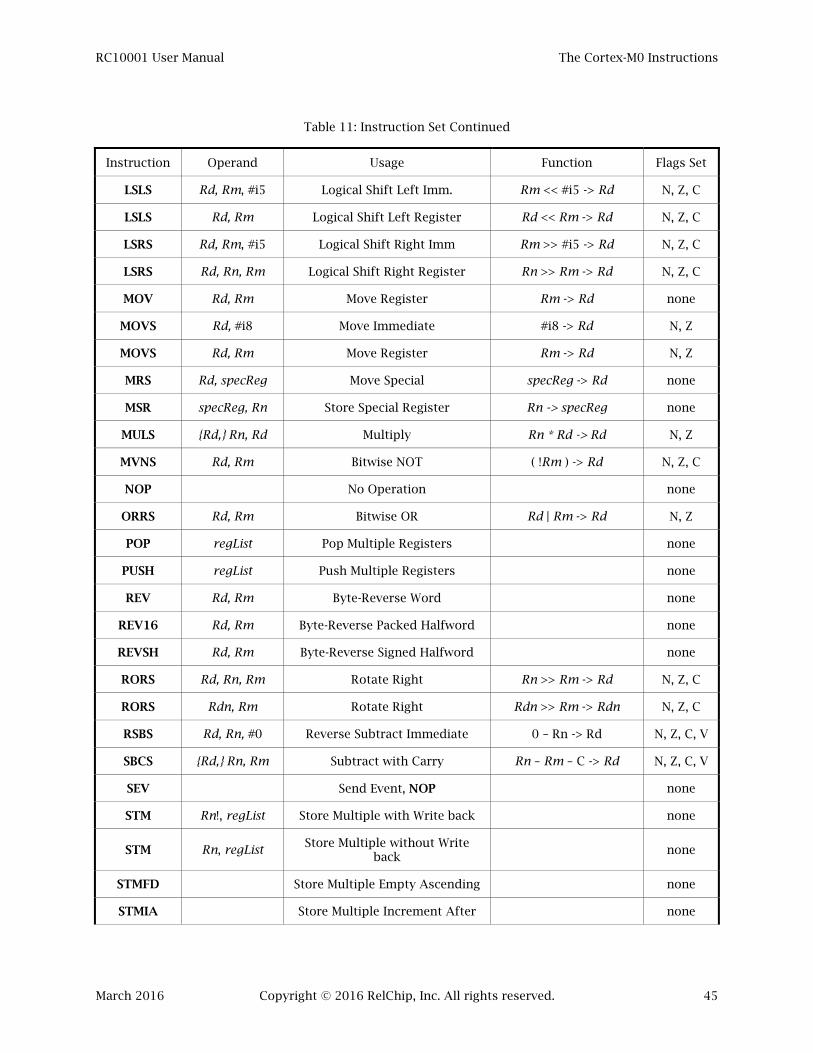
RC10001 User Manual The Cortex-M0 Instructions
March 2016 Copyright © 2016 RelChip, Inc. All rights reserved. 45
Table 11: Instruction Set Continued
Instruction Operand Usage Function Flags Set
LSLS Rd, Rm, #i5 Logical Shift Left Imm. Rm << #i5 -> Rd N, Z, C
LSLS Rd, Rm Logical Shift Left Register Rd << Rm -> Rd N, Z, C
LSRS Rd, Rm, #i5 Logical Shift Right Imm Rm >> #i5 -> Rd N, Z, C
LSRS Rd, Rn, Rm Logical Shift Right Register Rn >> Rm -> Rd N, Z, C
MOV Rd, Rm Move Register Rm -> Rd none
MOVS Rd, #i8 Move Immediate #i8 -> Rd N, Z
MOVS Rd, Rm Move Register Rm -> Rd N, Z
MRS Rd, specReg Move Special specReg -> Rd none
MSR specReg, Rn Store Special Register Rn -> specReg none
MULS {Rd,} Rn, Rd Multiply Rn * Rd -> Rd N, Z
MVNS Rd, Rm Bitwise NOT ( !Rm ) -> Rd N, Z, C
NOP No Operation none
ORRS Rd, Rm Bitwise OR Rd | Rm -> Rd N, Z
POP regList Pop Multiple Registers none
PUSH regList Push Multiple Registers none
REV Rd, Rm Byte-Reverse Word none
REV16 Rd, Rm Byte-Reverse Packed Halfword none
REVSH Rd, Rm Byte-Reverse Signed Halfword none
RORS Rd, Rn, Rm Rotate Right Rn >> Rm -> Rd N, Z, C
RORS Rdn, Rm Rotate Right Rdn >> Rm -> Rdn N, Z, C
RSBS Rd, Rn, #0 Reverse Subtract Immediate 0 – Rn -> Rd N, Z, C, V
SBCS {Rd,} Rn, Rm Subtract with Carry Rn – Rm – C -> Rd N, Z, C, V
SEV Send Event, NOP none
STM Rn!, regList Store Multiple with Write back none
STM Rn, regList Store Multiple without Write
back none
STMFD Store Multiple Empty Ascending none
STMIA Store Multiple Increment After none

RC10001 User Manual The Cortex-M0 Instructions
March 2016 Copyright © 2016 RelChip, Inc. All rights reserved. 46
Table 12: Instruction Set Continued
Instruction Operand Usage Function Flags Set
STR Rt, [Rn {,#i5}] Store Word Rt -> @[Rn + #i5] none
STR Rt, [SP {,#i8}] Store Word Rt -> @[SP + #i5] none
STR Rt, [Rn, Rm] Store Word Rt -> @[Rn + Rm] none
STRB Rt, [Rn {,#i5}] Store Byte Rt[7:0] -> @[Rn + #i5] none
STRB Rt, [Rn, Rm] Store Byte Rt[7:0] -> @[Rn + Rm] none
STRH Rt, [Rn {,#i5}] Store Halfword Rt[15:0] -> @[Rn + #i5] none
STRH Rt, [Rn, Rm] Store Halfword Rt[15:0] -> @[Rn + Rm] none
SUB Rd, SP, #i8 Subtract Immediate from SP SP + #i8 -> Rd none
SUB SP, #i7 Subtract Immediate from SP SP - #i7 -> SP none
SUB SP, SP, #i7 Subtract Immediate from SP SP - #i7 -> SP none
SUBS Rd, Rn, Rm Subtract Registers Rn - Rm -> Rd N, Z, C, V
SUBS Rdn, Rm Subtract Registers Rdn - Rm -> Rdn N, Z, C, V
SUBS Rd, #i8 Subtract Imm from Register Rd - #i8 -> Rd N, Z, C, V
SUBS Rd ,Rn, #i3 Subtract Imm from Register Rn - #i3 -> Rd N, Z, C, V
SVC #i8 Supervisor Call SVC Interrupt none
SXTB Rd, Rm Sign Extend Byte Sign ext Rm[7:0] -> Rd none
SXTH Rd, Rm Sign Extend Halfword Sign ext Rm[15:0] -> Rd none
TST Rn, Rm Logical AND Test Rn & Rm -> flags N, Z, C
UXTB Rd, Rm Unsigned Extend Byte Zero ext Rm[7:0] -> Rd none
UXTH Rd, Rm Unsigned Extend Halfword Zero ext Rm[15:0] -> Rd none
WFE Wait for Event none
WFI Wait for Interrupt none

RC10001 User Manual The Cortex-M0 Instructions
March 2016 Copyright © 2016 RelChip, Inc. All rights reserved. 47
7.2.1 Usage
7.2.1.1 ADCS – Add with Carry
Usage:
ADCS{q} {Rd,} Rd, Rm
Definitions:
q: Optional .N or .W Qualifier
Rd: Source and Destination Register (R0 to R7)
Rm: Source Register (R0 to R7)
Description: Rd + Rm + C -> Rd
Condition Flags Used: Carry (C)
Condition Flags Set: Negative (N), Zero (Z), Carry (C), Overflow (V)
Examples:
ADCS R1, R1, R3 ; R1 <- R1 + R3 + C
ADCS R5, R4 ; R5 <- R5 + R4 + C
7.2.1.2 ADD – Registers
Usage:
ADD Rd, Rm
Definitions:
Rd: Source and Destination Register (R0 to R14, SP, or LR)
Rm: Source Register (R0 to R14, SP, or LR)
Description: Rd + Rm -> Rd
Condition Flags Used: none
Condition Flags Set: none
Examples:
ADD R1, R12 ; R1 <- R1 + R12
ADD R5, PC ; R5 <- R5 + PC
Caveat: The use of the R15 or the PC can cause unpredictable results.

RC10001 User Manual The Cortex-M0 Instructions
March 2016 Copyright © 2016 RelChip, Inc. All rights reserved. 48
7.2.1.3 ADD – Immediate and Stack Pointer to Register
Usage:
ADD{q} Rd, SP, #i8
Definitions:
q: Optional .N or .W Qualifier
Rd: Destination Register (R0 to R7)
SP: Stack Pointer
#i8: Immediate Eight Bit Value, Shifted to get 0 to 1020 (in increments of 4)
Description: SP + (#i8 << 2) -> Rd
Condition Flags Used: none
Condition Flags Set: none
Examples:
ADD R1, SP, #64 ; R1 <- SP + #256
ADD R5, SP, #1 ; R5 <- SP + #4
7.2.1.4 ADD – Stack Pointer to Register
Usage:
ADD{q} Rd, SP, Rd
ADD{q} Rd, SP
Definitions:
q: Optional .N or .W Qualifier
Rd: Destination Register (R0 to R14, SP, or LR).
SP: Stack Pointer
Description: SP + Rd -> Rd
Condition Flags Used: none
Condition Flags Set: none
Examples:
ADD R1, SP, R1 ; R1 <- SP + R1
ADD R5, SP, R5 ; R5 <- SP + R5
Caveat: The use of the R15 or the PC can cause unpredictable results.
RC10001 User Manual The Cortex-M0 Instructions
March 2016 Copyright © 2016 RelChip, Inc. All rights reserved. 49
7.2.1.5 ADD – Register to Stack Pointer
Usage:
ADD{q} SP, Rm
Definitions:
q: Optional .N or .W Qualifier
Rm: Source Register (R0 to R14, SP, or LR)
SP: Stack Pointer
Description: SP + Rm -> SP
Condition Flags Used: none
Condition Flags Set: none
Examples:
ADD SP, R1 ; SP <- SP + R1
ADD SP, R5 ; SP <- SP + R5
Caveat: The use of the R15 or the PC can cause unpredictable results.
7.2.1.6 ADD – Immediate to Stack Pointer
Usage:
ADD{q} SP, #i7
ADD{q} SP, SP, #i7
Definitions:
q: Optional .N or .W Qualifier
SP: Stack Pointer
#i7: Immediate Seven Bit Value, Shifted to get 0 to 508 (in increments of 4)
Description: SP + (#i7 << 2) -> SP
Condition Flags Used: none
Condition Flags Set: none
Examples:
ADD SP, #64 ; SP <- SP + #256
ADD SP, #1 ; SP <- SP + #4

RC10001 User Manual The Cortex-M0 Instructions
March 2016 Copyright © 2016 RelChip, Inc. All rights reserved. 50
7.2.1.7 ADDS – Registers, Set Flags
Usage:
ADDS{q} Rd, Rm, Rn
ADDS{q} Rdn, Rm
Definitions:
q: Optional .N or .W Qualifier
Rd: Destination Register (R0 to R7)
Rm: First Source Register (R0 to R7)
Rn: Second Source Register (R0 to R7)
Description: Rm + Rn -> Rd, Rm + Rdn -> Rdn
Condition Flags Used: none
Condition Flags Set: Negative (N), Zero (Z), Carry (C), Overflow (V)
Examples:
ADDS R1, R2, R3 ; R1 <- R2 + R3
ADDS R5, R4, R5 ; R5 <- R4 + R5
7.2.1.8 ADDS – Immediate to Register, Set Flags
Usage:
ADDS{q} Rd, #i8
Definitions:
q: Optional .N or .W Qualifier
Rd: Destination Register (R0 to R7)
#i8: Immediate Eight Bit Value, 0 to 255
Description: Rd + #i8 -> Rd
Condition Flags Used: none
Condition Flags Set: Negative (N), Zero (Z), Carry (C), Overflow (V)
Examples:
ADDS R1, #5 ; R1 <- R1 + 5
ADDS R5, #255 ; R5 <- R5 + 255

RC10001 User Manual The Cortex-M0 Instructions
March 2016 Copyright © 2016 RelChip, Inc. All rights reserved. 51
7.2.1.9 ADDS – Immediate and Register to Register, Set Flags
Usage:
ADDS{q} Rd, Rn, #i3
Definitions:
q: Optional .N or .W Qualifier
Rd: Destination Register (R0 to R7)
Rn: Source Register (R0 to R7)
#i3: Immediate Three Bit Value, 0 to 7
Description: Rn + #i3 -> Rd
Condition Flags Used: none
Condition Flags Set: Negative (N), Zero (Z), Carry (C), Overflow (V)
Examples:
ADDS R1, R2, #1 ; R1 <- R2 + 1
ADDS R5, R4, #7 ; R5 <- R4 + 7
7.2.1.10 ADR – Immediate and PC to Register
Usage:
ADR{q} Rd, #lab8
Definitions:
q: Optional .N or .W Qualifier
Rd: Destination Register (R0 to R7)
#lab8: Eight Bit Offset to a Label (0 to 1020 after the internal shift)
Description: PC + #lab8 -> Rd
Condition Flags Used: none
Condition Flags Set: none
Examples:
ADR R1, =foo ; R1 <- PC + offset to foo
ADR R5, #255 ; R5 <- PC + 1020

RC10001 User Manual The Cortex-M0 Instructions
March 2016 Copyright © 2016 RelChip, Inc. All rights reserved. 52
7.2.1.11 ANDS – Bitwise AND
Usage:
ANDS{q} Rd, Rm
Definitions:
q: Optional .N or .W Qualifier
Rd: Source and Destination Register (R0 to R7)
Rm: Source Register (R0 to R7)
Description: Rd & Rm -> Rd
Condition Flags Used: none
Condition Flags Set: Negative (N), Zero (Z).
Examples:
ANDS R1, R2 ; R1 <- R1 & R2
ANDS R5, R4 ; R5 <- R5 & R4
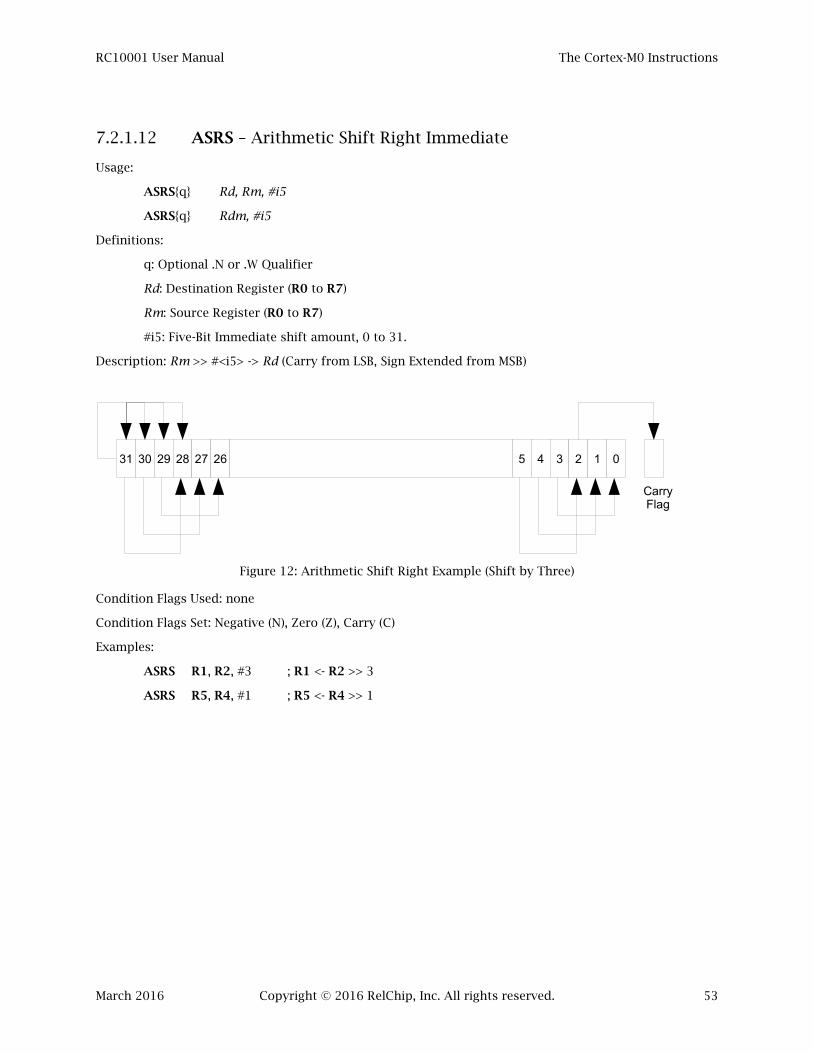
RC10001 User Manual The Cortex-M0 Instructions
March 2016 Copyright © 2016 RelChip, Inc. All rights reserved. 53
7.2.1.12 ASRS – Arithmetic Shift Right Immediate
Usage:
ASRS{q} Rd, Rm, #i5
ASRS{q} Rdm, #i5
Definitions:
q: Optional .N or .W Qualifier
Rd: Destination Register (R0 to R7)
Rm: Source Register (R0 to R7)
#i5: Five-Bit Immediate shift amount, 0 to 31.
Description: Rm >> #<i5> -> Rd (Carry from LSB, Sign Extended from MSB)
Figure 12: Arithmetic Shift Right Example (Shift by Three)
Condition Flags Used: none
Condition Flags Set: Negative (N), Zero (Z), Carry (C)
Examples:
ASRS R1, R2, #3 ; R1 <- R2 >> 3
ASRS R5, R4, #1 ; R5 <- R4 >> 1
31 30 29 28 27 26 5 4 3 2 1 0
CarryFlag

RC10001 User Manual The Cortex-M0 Instructions
March 2016 Copyright © 2016 RelChip, Inc. All rights reserved. 54
7.2.1.13 ASRS – Arithmetic Shift Right Register
Usage:
ASRS{q} Rd, Rm
Definitions:
q: Optional .N or .W Qualifier
Rd: Destination Register (R0 to R7)
Rm: Shift Count Register (R0 to R7)
Description: Rd >> Rm -> Rd (Carry from LSB, Sign Extended from MSB)
Condition Flags Used: none
Condition Flags Set: Negative (N), Zero (Z), Carry (C)
Examples:
ASRS R1, R2 ; R1 <- R1 >> R2
ASRS R5, R4 ; R5 <- R5 >> R4
7.2.1.14 B – Branch-Unconditional
Usage:
B{q} #lab11
Definitions:
q: Optional .N or .W Qualifier
#lab11: Address Offset (-2048 to 2046) of the label from PC, halfword aligned
Description: PC + #lab11 -> PC
Condition Flags Used: none
Condition Flags Set: none
Examples:
B FOO ; go to FOO
B bar ; go to bar
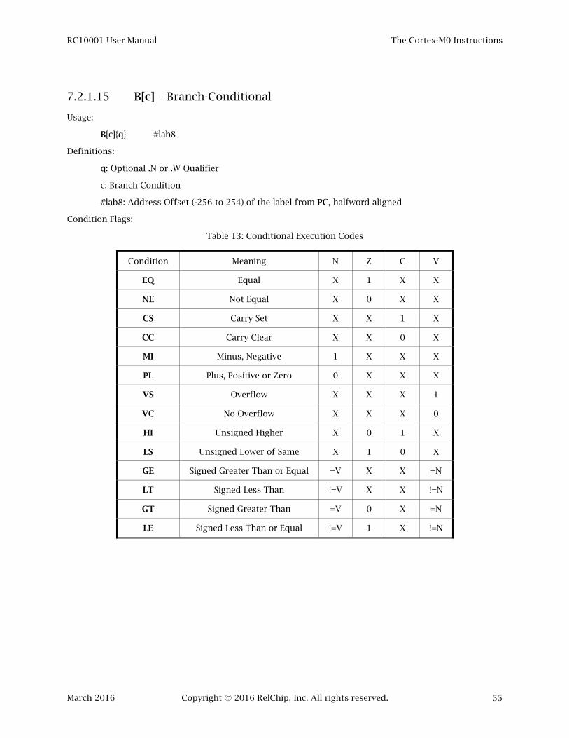
RC10001 User Manual The Cortex-M0 Instructions
March 2016 Copyright © 2016 RelChip, Inc. All rights reserved. 55
7.2.1.15 B[c] – Branch-Conditional
Usage:
B[c]{q} #lab8
Definitions:
q: Optional .N or .W Qualifier
c: Branch Condition
#lab8: Address Offset (-256 to 254) of the label from PC, halfword aligned
Condition Flags:
Table 13: Conditional Execution Codes
Condition Meaning N Z C V
EQ Equal X 1 X X
NE Not Equal X 0 X X
CS Carry Set X X 1 X
CC Carry Clear X X 0 X
MI Minus, Negative 1 X X X
PL Plus, Positive or Zero 0 X X X
VS Overflow X X X 1
VC No Overflow X X X 0
HI Unsigned Higher X 0 1 X
LS Unsigned Lower of Same X 1 0 X
GE Signed Greater Than or Equal =V X X =N
LT Signed Less Than !=V X X !=N
GT Signed Greater Than =V 0 X =N
LE Signed Less Than or Equal !=V 1 X !=N

RC10001 User Manual The Cortex-M0 Instructions
March 2016 Copyright © 2016 RelChip, Inc. All rights reserved. 56
Description: if condition then PC + #lab8 -> PC
else PC + 2 -> PC
Condition Flags Used: one or more to test the condition from the full set
Condition Flags Set: none
Examples:
BLT lessThan ; If less than condition, go to address lessThan
BEQ zEqual ; if equal (used for zero also), go to zEqual
7.2.1.16 BICS – Bitwise AND with Complement
Usage:
BICS{q} Rd, Rm
Definitions:
q: Optional .N or .W Qualifier
Rd: Source and Destination Register (R0 to R7)
Rm: Source Register (R0 to R7)
Description: Rd & (!Rm) -> Rd
Condition Flags Used: none
Condition Flags Set: Negative (N), Zero (Z).
Examples:
BICS R1, R2 ; R1 <- R1 & (!R2)
BICS R5, R4 ; R5 <- R5 & (!R4)
7.2.1.17 BKPT – Breakpoint
Usage:
BKPT #i8
Definitions:
#i8: Immediate Eight Bit Constant (0 to 255)
Description: Break into the Debugger (if enabled), otherwise Hardfault
Examples:
BKPT #15 ; Breakpoint identified as #15

RC10001 User Manual The Cortex-M0 Instructions
March 2016 Copyright © 2016 RelChip, Inc. All rights reserved. 57
7.2.1.18 BL – Branch with Link
Usage:
BL{q} #lab25
Definitions:
q: Optional .N or .W Qualifier
#lab25: Address Offset (-16MB to 16MB) of the label from PC
Description: PC + 2 -> LR; PC + #lab25 -> PC
Note: This is a thirty-two bit instruction.
Condition Flags Used: none
Condition Flags Set: none
Examples:
BL FOO ; call FOO
BL bar ; call bar
7.2.1.19 BLX – Branch with Link and Exchange
Usage:
BLX{q} Rm
Definitions:
q: Optional .N or .W Qualifier
Rm: Destination Address
Description: PC + 2 ->LR; Rm -> PC
Condition Flags Used: none
Condition Flags Set: none
Exceptions: Non-Thumb-2 Address (Bit [0] != 1) causes Hardfault
Examples:
BLX R1 ; call @[R1]
BLX R5 ; call @[R5]

RC10001 User Manual The Cortex-M0 Instructions
March 2016 Copyright © 2016 RelChip, Inc. All rights reserved. 58
7.2.1.20 BX – Branch and Exchange
Usage:
BX{q} Rm
Definitions:
q: Optional .N or .W Qualifier
Rm: Destination Address
Description: Rm -> PC
Condition Flags Used: none
Condition Flags Set: none
Exceptions: Non-Thumb-2 Address (Bit [0] != 1) causes Hardfault
Examples:
BX R1 ; go to R1
BX R5 ; go to R5
7.2.1.21 CMN – Compare Negative
Usage:
CMN{q} Rn, Rm
Definitions:
q: Optional .N or .W Qualifier
Rn: Source Register (R0 to R7), not inverted.
Rm: Source Register (R0 to R7), bitwise not before compare.
Description: Rn - (!Rm) -> Condition Codes
Condition Flags Used: none
Condition Flags Set: Negative (N), Zero (Z), Carry (C), Overflow (V)
Examples:
CMN R1, R2 ; Condition <- R1 & (!R2)
CMN R5, R4 ; Condition <- R5 & (!R4)

RC10001 User Manual The Cortex-M0 Instructions
March 2016 Copyright © 2016 RelChip, Inc. All rights reserved. 59
7.2.1.22 CMP – Compare Immediate
Usage:
CMP{q} Rn, #i8
Definitions:
q: Optional .N or .W Qualifier
Rn: Source Register (R0 to R7)
#i8: immediate from 0 to 255
Description: Rn - #i8 -> Condition Codes
Condition Flags Used: none
Condition Flags Set: Negative (N), Zero (Z), Carry (C), Overflow (V)
Examples:
CMP R1, #5 ; Condition <- R1 - #5
CMP R5, #25 ; Condition <- R5 - #25
7.2.1.23 CMP – Compare Register
Usage:
CMP{q} Rn, Rm
Definitions:
q: Optional .N or .W Qualifier
Rn: Source Register (R0 to R7)
Rm: Source Register (R0 to R7)
Description: Rm - Rn -> Condition Codes
Condition Flags Used: none
Condition Flags Set: Negative (N), Zero (Z), Carry (C), Overflow (V)
Examples:
CMP R1, R2 ; Condition <- R2 – R1
CMP R5, R4 ; Condition <- R4 – R5

RC10001 User Manual The Cortex-M0 Instructions
March 2016 Copyright © 2016 RelChip, Inc. All rights reserved. 60
7.2.1.24 CPSID – Disable PRIMASK Exception
Usage:
CPSID i
Definitions:
i: Set to 1 to raise priority to 0
Description: PRIMASK.PM to 1
Examples:
CPSID 1 ; Disable Exceptions, Raise Priority to 0
7.2.1.25 CPSIE – Enable PRIMASK Exception
Usage:
CPSIE i
Definitions:
i: Set to 1 to raise priority to 0
Description: PRIMASK.PM to 0
Examples:
CPSIE 1 ; Enable Exceptions, Raise Priority to 0
7.2.1.26 DMB – Data Memory Barrier
Usage:
DMB{q} {opt}
Definitions:
q: Optional .N or .W Qualifier
opt: Optional, only allowed as 0xf
Description: Stops memory accesses until all pending accesses are complete. The RC10001 insures operation ordering to every memory address so this should not be required. This is a thirty-two bit instruction.
Examples:
DMB ; Memory Barrier

RC10001 User Manual The Cortex-M0 Instructions
March 2016 Copyright © 2016 RelChip, Inc. All rights reserved. 61
7.2.1.27 DSB – Data Synchronization Barrier
Usage:
DMB{q} {opt}
Definitions:
q: Optional .N or .W Qualifier
opt: Optional, only set to 0xf
Description: Stops instruction execution until all pending memory accesses are complete. The RC10001 insures operation ordering to every memory address so this should not be required. This is a thirty-two bit instruction.
Examples:
DMB ; Synchronization Barrier
7.2.1.28 EORS – Bitwise Exclusive OR
Usage:
EORS{q} Rd, Rm
Definitions:
q: Optional .N or .W Qualifier
Rd: Source and Destination Register (R0 to R7)
Rm: Source Register (R0 to R7)
Description: Rd ^ Rm -> Rd
Condition Flags Used: none
Condition Flags Set: Negative (N), Zero (Z).
Examples:
EORS R1, R2 ; R1 <- R1 ^ R2
EORS R5, R4 ; R5 <- R5 ^ R4

RC10001 User Manual The Cortex-M0 Instructions
March 2016 Copyright © 2016 RelChip, Inc. All rights reserved. 62
7.2.1.29 ISB – Instruction Synchronization Barrier
Usage:
ISB{q} {opt}
Definitions:
q: Optional .N or .W Qualifier
opt: Optional, only set to 0xf
Description: Stops instruction execution until all pending instructions are complete. Changes to the CONTROL register should be followed by the ISB command to insure those changes take effect. This is a thirty-two bit instruction.
Examples:
ISB ; Synchronization Barrier
7.2.1.30 LDM – Load Multiple with Write Back
Usage:
LDM{q} Rn!, regList
Definitions:
q: Optional .N or .W Qualifier
Rn: Address Register (R0 to R7), not included in the register list.
regList: register list.
Description: Each register in the list is loaded from memory, the first from the address specified by Rn, then next from Rn + 4, etc. Rn is updated with the address used. Rn cannot be in the register list.
Condition Flags Used: none
Condition Flags Set: none
Examples:
LDM R1!, {R2, R4, R3} ; Loads in order R2, R3, and R4 from the sequence in R1
LDM R5!, {R0-R4} ; Loads R0 to R4 from the sequence in R5
RC10001 User Manual The Cortex-M0 Instructions
March 2016 Copyright © 2016 RelChip, Inc. All rights reserved. 63
7.2.1.31 LDM – Load Multiple without Write Back
Usage:
LDM{q} Rn, regList
Definitions:
q: Optional .N or .W Qualifier
Rn: Address Register (R0 to R7), is included in the register list.
regList: register list.
Description: Each register in the list is loaded from memory, the first from the address specified by Rn, then next from Rn + 4, etc. Rn must be in the register list.
Condition Flags Used: none
Condition Flags Set: none
Exceptions: Hardfault
Examples:
LDM R1, {R2, R4, R1} ; Loads in order R1, R2, and R4 from the sequence in R1
LDM R0, {R0-R4} ; Loads R0 to R4 from the sequence in R0
7.2.1.32 LDMFD – Load Memory Full Descending
Synonym for LDM.
7.2.1.33 LDMIA – Load Memory Increment Address
Synonym for LDM.

RC10001 User Manual The Cortex-M0 Instructions
March 2016 Copyright © 2016 RelChip, Inc. All rights reserved. 64
7.2.1.34 LDR – Load Word @[Register Plus Immediate] -> Register
Usage:
LDR{q} Rt, [Rn {,#i5}]
Definitions:
q: Optional .N or .W Qualifier
Rt: Destination Register (R0 to R7)
Rn: Base Address Register (R0 to R7)
#i5: Immediate Five Bit Value (0 to 124 after shift left two)
Description: @[Rn + (#i5 << 4)] -> Rt
Condition Flags Used: none
Condition Flags Set: none
Exceptions: Hardfault
Examples:
LDR R1, [R2, #5] ; R1 <- @[R2+20]
LDR R5, [R5, #31] ; R5 <- @[R5+124]
7.2.1.35 LDR – Load Word @ SP Plus Immediate -> Register
Usage:
LDR{q} Rt, [SP {,#i8}]
Definitions:
q: Optional .N or .W Qualifier
Rt: Destination Register (R0 to R7)
#i8: Immediate Eight Bit Value (0 to 1020 after shift left two)
Description: @[SP + (#i8 << 4)] -> Rt
Condition Flags Used: none
Condition Flags Set: none
Exceptions: Hardfault
Examples:
LDR R1, [SP, #5] ; R1 <- @[SP+20]
LDR R5, [SP, #255] ; R5 <- @[R5+1020]
RC10001 User Manual The Cortex-M0 Instructions
March 2016 Copyright © 2016 RelChip, Inc. All rights reserved. 65
7.2.1.36 LDR – Load Word Label@[PC + offset] -> Register
Usage:
LDR{q} Rt, =label
Definitions:
q: Optional .N or .W Qualifier
Rt: Destination Register (R0 to R7)
=label: label within 0-1020 offset of PC
Description: @[label] -> Rt
Condition Flags Used: none
Condition Flags Set: none
Exceptions: Hardfault
Examples:
LDR R1, =FOO ; R1 <- offset to label FOO
LDR R5, #1 ; R5 <- #4
7.2.1.37 LDR – Load Word @[Register Plus Register] -> Register
Usage:
LDR{q} Rt, [Rn, Rm]
Definitions:
q: Optional .N or .W Qualifier
Rt: Destination Register (R0 to R7)
Rn: Base Address Register (R0 to R7)
Rm: Offset Address Register (R0 to R7)
Description: @[Rd + Rm] -> Rt
Condition Flags Used: none
Condition Flags Set: none
Examples:
LDR R1, [R2, R3] ; R1 <- @[R2+R3]
LDR R5, [R5, R4] ; R5 <- @[R5+R4]
RC10001 User Manual The Cortex-M0 Instructions
March 2016 Copyright © 2016 RelChip, Inc. All rights reserved. 66
7.2.1.38 LDRB – Load Unsigned Byte…@ Register Plus Immediate to Register
Usage:
LDRB{q} Rt, [Rn {,#i5}]
Definitions:
q: Optional .N or .W Qualifier
Rt: Destination Register (R0 to R7)
Rn: Source Register (R0 to R7)
#i5: Immediate Five Bit Value, 0 to 31
Description: Byte@[Rn + #i5] & 0x0000_00FF -> Rt (i.e. 0 extended byte)
Condition Flags Used: none
Condition Flags Set: none
Examples:
LDRB R1, [R2, #5] ; R1 <- Byte @[R2+5]
LDRB R5, [R5, #31] ; R5 <- Byte @[R5+31]
7.2.1.39 LDRB – Load Unsigned Byte…@ Register Plus Register to Register
Usage:
LDRB{q} Rt, [Rn, Rm]
Definitions:
q: Optional .N or .W Qualifier
Rt: Destination Register (R0 to R7)
Rn: Source Register (R0 to R7)
Rm: Source Register (R0 to R7)
Description: Byte@[Rd + Rm] &0x0000_00FF -> Rt (i.e. 0 extended byte)
Condition Flags Used: none
Condition Flags Set: none
Examples:
LDRB R1, [R2, R3] ; R1 <- Byte @[R2+R3]
LDRB R5, [R5, R4] ; R5 <- Byte @[R5+R4]
RC10001 User Manual The Cortex-M0 Instructions
March 2016 Copyright © 2016 RelChip, Inc. All rights reserved. 67
7.2.1.40 LDRH – Load Unsigned Halfword…@ Register Plus Immediate to Register
Usage:
LDRH{q} Rt, [Rn {,#i5}]
Definitions:
q: Optional .N or .W Qualifier
Rt: Destination Register (R0 to R7)
Rn: Source Register (R0 to R7)
#i5: Immediate Five Bit Value, 0 to 62 (Shifted 1)
Description: Halfword@[Rd + (#i5 << 1)] & 0x0000_FFFF -> Rt (i.e. 0 extended)
Condition Flags Used: none
Condition Flags Set: none
Examples:
LDRH R1, [R2, #5] ; R1 <- Halfword @[R2+10]
LDRH R5, [R5, #31] ; R5 <- Halfword @[R5+62]
7.2.1.41 LDRH – Load Unsigned Halfword…@ Register Plus Register to Register
Usage:
LDRH{q} Rt, [Rn, Rm]
Definitions:
q: Optional .N or .W Qualifier
Rt: Destination Register (R0 to R7)
Rn: Source Register (R0 to R7)
Rm: Source Register (R0 to R7)
Description: Byte@[Rd + Rm] &0x0000_FFFF -> Rt (i.e. 0 extended)
Condition Flags Used: none
Condition Flags Set: none
Examples:
LDRH R1, [R2, R3] ; R1 <- Halfword @[R2+R3]
LDRH R5, [R5, R4] ; R5 <- Halfword @[R5+R4]

RC10001 User Manual The Cortex-M0 Instructions
March 2016 Copyright © 2016 RelChip, Inc. All rights reserved. 68
7.2.1.42 LDRSB – Load Signed Byte…@ Register Plus Register to Register
Usage:
LDRSB{q} Rt, [Rn, Rm]
Definitions:
q: Optional .N or .W Qualifier
Rt: Destination Register (R0 to R7)
Rn: Source Register (R0 to R7)
Rm: Source Register (R0 to R7)
Description: Byte@[Rd + Rm] extend by d[7] -> Rt (i.e. sign extended byte)
Condition Flags Used: none
Condition Flags Set: none
Examples:
LDRSB R1, [R2, R3] ; R1 <- Byte @[R2+R3]
LDRSB R5, [R5, R4] ; R5 <- Byte @[R5+R4]
7.2.1.43 LDRSH – Load Signed Halfword…@ Register Plus Register to Register
Usage:
LDRSH{q} Rt, [Rn, Rm]
Definitions:
q: Optional .N or .W Qualifier
Rt: Destination Register (R0 to R7)
Rn: Source Register (R0 to R7)
Rm: Source Register (R0 to R7)
Description: Byte@[Rd + Rm] extended by D[15] -> Rt (i.e. sign extended)
Condition Flags Used: none
Condition Flags Set: none
Examples:
LDRSH R1, [R2, R3] ; R1 <- Halfword @[R2+R3]
LDRSH R5, [R5, R4] ; R5 <- Halfword @[R5+R4]

RC10001 User Manual The Cortex-M0 Instructions
March 2016 Copyright © 2016 RelChip, Inc. All rights reserved. 69
7.2.1.44 LSLS – Logical Shift Left Immediate
Usage:
LSLS{q} Rd., Rm, #i5
LSLS{q} Rdm, #i5
Definitions:
q: Optional .N or .W Qualifier
Rd: Destination Register (R0 to R7)
Rm: Source Register (R0 to R7)
#i5: Five Bit Shift Amount, 0 to 31.
Description: Rm << #<i5> -> Rd (Shift in zero)
Figure 13: Logical Shift Left Example (Shift by Three)
Condition Flags Used: none
Condition Flags Set: Negative (N), Zero (Z), Carry (C)
Examples:
LSLS R1, R2, #3 ; R1 <- R2 << 3
LSLS R5, R4, #1 ; R5 <- R4 << 1
31 30 29 28 27 26 5 4 3 2 1 0
CarryFlag
0

RC10001 User Manual The Cortex-M0 Instructions
March 2016 Copyright © 2016 RelChip, Inc. All rights reserved. 70
7.2.1.45 LSLS – Logical Shift Left Register
Usage:
LSLS{q} Rd, Rm
Definitions:
q: Optional .N or .W Qualifier
Rd: Destination Register (R0 to R7)
Rm: Shift Count Register (R0 to R7)
Description: Rd << Rm -> Rd (Shift in zero)
Condition Flags Used: none
Condition Flags Set: Negative (N), Zero (Z), Carry (C)
Examples:
LSLS R1, R2 ; R1 <- R1 << R2
LSLS R5, R4 ; R5 <- R5 << R4
7.2.1.46 LSRS – Logical Shift Right (Register >> Immediate) -> Register
Usage:
LSRS{q} Rd., Rm, #i5
LSRS{q} Rdm, #i5
Definitions:
q: Optional .N or .W Qualifier
Rd: Destination Register (R0 to R7)
Rm: Source Register (R0 to R7)
#i5: Five Bit Shift Amount, 0 to 31.
Description: (Rm >> #i5) -> Rd (Shift in zero)
Condition Flags Used: none
Condition Flags Set: Negative (N), Zero (Z), Carry (C)
Examples:
LSRS R1, R2, #3 ; R1 <- R2 >> 3
LSRS R5, R4, #1 ; R5 <- R4 >> 1
RC10001 User Manual The Cortex-M0 Instructions
March 2016 Copyright © 2016 RelChip, Inc. All rights reserved. 71
7.2.1.47 LSRS – Logical Shift Right (Register >> Register) -> Register
Usage:
LSRS{q} Rd, Rn, Rm
Definitions:
q: Optional .N or .W Qualifier
Rd: Destination Register (R0 to R7)
Rm: Shift Count Register (R0 to R7)
Description: Rd >> Rm -> Rd (Shift in zero)
Condition Flags Used: none
Condition Flags Set: Negative (N), Zero (Z), Carry (C)
Examples:
LSRS R1, R2 ; R1 <- R1 >> R2
LSRS R5, R4 ; R5 <- R5 >> R4
7.2.1.48 MOV – Move Register -> Register
Usage:
MOV Rd, Rm
Definitions:
q: Optional .N or .W Qualifier
Rd: Destination Register (R0 to R12, LR, SP, or PC)
Rm: Source Register (R0 to R12, LR, SP, or PC)
Description: Rm -> Rd
Condition Flags Used: none
Condition Flags Set: none
Note: MOV Rd, PC does not set bit[0] for a valid return address.
Examples:
MOV R1, R2 ; R1 <- R2
MOV R5, R12 ; R5 <- R12

RC10001 User Manual The Cortex-M0 Instructions
March 2016 Copyright © 2016 RelChip, Inc. All rights reserved. 72
7.2.1.49 MOVS – Move Immediate -> Register
Usage:
MOVS{q} Rd, #i8
Definitions:
q: Optional .N or .W Qualifier
Rd: Destination Register (R0 to R7)
#i8: Immediate Eight Bit Value, 0 to 255
Description: #i8 -> Rd (zero extended)
Condition Flags Used: none
Condition Flags Set: Negative (N), Zero (Z)
Examples:
MOVS R1, #25 ; R1 <- #25
MOVS R5, #255 ; R5 <- #255
7.2.1.50 MOVS – Move Register -> Register
Usage:
MOVS{q} Rd, Rm
Definitions:
q: Optional .N or .W Qualifier
Rd: Destination Register (R0 to R7)
Rm: Source Register (R0 to R7)
Description: Rm -> Rd
Condition Flags Used: none
Condition Flags Set: Negative (N), Zero (Z)
Examples:
MOVS R1, R2 ; R1 <- R2
MOVS R5, R4 ; R5 <- R4

RC10001 User Manual The Cortex-M0 Instructions
March 2016 Copyright © 2016 RelChip, Inc. All rights reserved. 73
7.2.1.51 MRS – Move Special Register to Register
Usage:
MRS{q} Rd, specReg
Definitions:
q: Optional .N or .W Qualifier
Rd: Destination Register (R0 to R7)
specReg: Source Special Register (see Table 14)
Description: specReg -> Rd
Note: This is a thirty-two bit instruction.
Table 14: Special Registers
Register Description
APSR Flags from Previous Instruction
IPSR Interrupt Status Register
EPSR Exception Status Register
IAPSR Bitwise IPSR or APSR
EAPSR Bitwise EPSR or APSR
IEPSR Bitwise IPSR or EPSR
XPSR Bitwise IPSR or EPSR or APSR
MSP Main Stack Pointer
PSP Process Stack Pointer
PRIMASK Mask Configurable Exceptions
CONTROL Control Register
Condition Flags Used: none
Condition Flags Set: none
Examples:
MRS R1, IPSR ; R1 <- IPSR
MRS R5, MSP ; R5 <- MSP

RC10001 User Manual The Cortex-M0 Instructions
March 2016 Copyright © 2016 RelChip, Inc. All rights reserved. 74
7.2.1.52 MSR – Move Register to Special Register
Usage:
MSR{q} specReg, Rn
Definitions:
q: Optional .N or .W Qualifier
specReg: Destination Special Register (see Table 14)
Rn: Source Register (R0 to R7)
Description: Rm * Rn -> Rd
Condition Flags Used: none
Condition Flags Set: none
Examples:
MSR IPSR, R1 ; IPSR -> R1
MSR MSP, R5 ; MSP -> R5
7.2.1.53 MULS – Multiply
Usage:
MULS{q} {Rd,} Rn, Rd
Definitions:
q: Optional .N or .W Qualifier
Rd: Destination Register (R0 to R7)
Rn: Source Register (R0 to R7)
Description: Rn * Rd -> Rd
Condition Flags Used: none
Condition Flags Set: Negative (N), Zero (Z)
Examples:
MULS R2, R1 ; R2 * R1 -> R1
MULS R4, R5 ; R4 * R5 -> R5

RC10001 User Manual The Cortex-M0 Instructions
March 2016 Copyright © 2016 RelChip, Inc. All rights reserved. 75
7.2.1.54 MVNS – Bitwise NOT (!Register) -> Register
Usage:
MVNS{q} Rd, Rm
Definitions:
q: Optional .N or .W Qualifier
Rd: Destination Register (R0 to R7)
Rm: Source Register (R0 to R7)
Description: !Rm -> Rd
Condition Flags Used: none
Condition Flags Set: Negative (N), Zero (Z), Carry (C)
Examples:
MVNS R1, R2 ; !R2 -> R1
MVNS R5, R4 ; !R4 -> R5
7.2.1.55 NOP – No Operation
Usage:
NOP{q}
Definitions:
q: Optional .N or .W Qualifier
Description: No Operation
Condition Flags Used: none
Condition Flags Set: none
Examples:
NOP ; No Operation

RC10001 User Manual The Cortex-M0 Instructions
March 2016 Copyright © 2016 RelChip, Inc. All rights reserved. 76
7.2.1.56 ORRS – Bitwise OR
Usage:
ORRS{q} Rd, Rm
Definitions:
q: Optional .N or .W Qualifier
Rd: Source and Destination Register (R0 to R7)
Rm: Source Register (R0 to R7)
Description: Rd | Rm -> Rd
Condition Flags Used: none
Condition Flags Set: Negative (N), Zero (Z).
Examples:
ORRS R1, R2 ; R1 <- R1 | R2
ORRS R5, R4 ; R5 <- R5 | R4
7.2.1.57 POP – Pop Multiple Registers
Usage:
POP{q} regList
Definitions:
q: Optional .N or .W Qualifier
regList: register list.
Description: Each register in the list is popped from the stack in descending order of the registers.
Condition Flags Used: none
Condition Flags Set: none
Examples:
POP {R2, R4, R1} ; Loads in order R4, R2, and R1 from the stack
POP {R0-R4} ; Loads R4 to R0 from the stack

RC10001 User Manual The Cortex-M0 Instructions
March 2016 Copyright © 2016 RelChip, Inc. All rights reserved. 77
7.2.1.58 PUSH – Push Multiple Registers
Usage:
PUSH{q} regList
Definitions:
q: Optional .N or .W Qualifier
regList: register list.
Description: Each register in the list is pushed onto the stack in ascending order of the registers.
Condition Flags Used: none
Condition Flags Set: none
Examples:
PUSH {R2, R4, R1} ; Stores in order R1, R2, and R4 onto the stack
PUSH {R0-R4} ; Stores R0 to R4 onto the stack
7.2.1.59 REV – Byte-Reverse Word
Usage:
REV{q} Rd, Rm
Definitions:
q: Optional .N or .W Qualifier
Rd: Source and Destination Register (R0 to R7)
Rm: Source Register (R0 to R7)
Description: Rm[7:0] -> Rd[31:24], Rm[15:8] -> Rd[23:16], Rm[23:16] -> Rd[15:8], Rm[31:24] -> Rd[7:0]
Condition Flags Used: none
Condition Flags Set: none
Examples:
REV R1, R2 ; R1 <- reordered R2
REV R5, R4 ; R5 <- reordered R4

RC10001 User Manual The Cortex-M0 Instructions
March 2016 Copyright © 2016 RelChip, Inc. All rights reserved. 78
7.2.1.60 REV16 – Byte-Reverse Packed Halfword
Usage:
REV16{q} Rd, Rm
Definitions:
q: Optional .N or .W Qualifier
Rd: Source and Destination Register (R0 to R7)
Rm: Source Register (R0 to R7)
Description: Rm[7:0] -> Rd[15:8], Rm[15:8] -> Rd[7:0], Rm[23:16] -> Rd[31:24], Rm[31:24] -> Rd[23:16]
Condition Flags Used: none
Condition Flags Set: none
Examples:
REV16 R1, R2 ; R1 <- reordered R2
REV16 R5, R4 ; R5 <- reordered R4
7.2.1.61 REVSH – Byte-Reverse Signed Halfword
Usage:
REVSH{q} Rd, Rm
Definitions:
q: Optional .N or .W Qualifier
Rd: Source and Destination Register (R0 to R7)
Rm: Source Register (R0 to R7)
Description: Rm[7:0] -> Rd[15:8] (sign extended to [31]), Rm[15:8] -> Rd[7:0]
Condition Flags Used: none
Condition Flags Set: none
Examples:
REVSH R1, R2 ; R1 <- reordered R2, sign extended
REVSH R5, R4 ; R5 <- reordered R4, sign extended

RC10001 User Manual The Cortex-M0 Instructions
March 2016 Copyright © 2016 RelChip, Inc. All rights reserved. 79
7.2.1.62 RORS – Rotate Right Register
Usage:
RORS{q} Rd, Rm, Rn
RORS{q} Rdn, Rm
Definitions:
q: Optional .N or .W Qualifier
Rd: Destination Register (R0 to R7)
Rm: Shift Count Register (R0 to R7)
Rn: Source Register (R0 to R7) same as Rd
Description: Rd >> Rm -> Rd (Rotate in bit 0), Rn >> Rm -> Rd
Figure 14: Rotate Right by Three Example
Condition Flags Used: none
Condition Flags Set: Negative (N), Zero (Z), Carry (C)
Examples:
RORS R1, R2 ; R1 <- R1 >> R2
RORS R5, R4 ; R5 <- R5 >> R4
31 30 29 28 27 26 5 4 3 2 1 0
CarryFlag

RC10001 User Manual The Cortex-M0 Instructions
March 2016 Copyright © 2016 RelChip, Inc. All rights reserved. 80
7.2.1.63 RSBS – Reverse Subtract Register from an Immediate Register, Set Flags
Usage:
RSBS{q} Rd, Rn, #0
Definitions:
q: Optional .N or .W Qualifier
Rd: Destination Register (R0 to R7)
Rn: Source Register (R0 to R7)
#0: Only zero Immediate Value Accepted
Description: 0 - Rn -> Rd
Condition Flags Used: none
Condition Flags Set: Negative (N), Zero (Z), Carry (C), Overflow (V)
Examples:
RSBS R1, R2, #0 ; R1 <- 0 - R2
RSBS R5, R4, #0 ; R5 <- 0 - R4
7.2.1.64 SBCS – Subtract with Carry, Set Flags
Usage:
SBCS{q} {Rd,} Rn, Rm
Definitions:
q: Optional .N or .W Qualifier
Rd: Destination Register (R0 to R7)
Rn: Source Register (R0 to R7)
Rm: Source Register (R0 to R7)
Description: Rn – Rm - C -> Rd
Condition Flags Used: Carry (C)
Condition Flags Set: Negative (N), Zero (Z), Carry (C), Overflow (V)
Examples:
SBCS R1, R2, R3 ; R1 <- R2 – R3
RSBS R5, R4, R5 ; R5 <- R4 – R5
RC10001 User Manual The Cortex-M0 Instructions
March 2016 Copyright © 2016 RelChip, Inc. All rights reserved. 81
7.2.1.65 SEV – Send Event, NOP
Usage:
SEV{q}
Definitions:
q: Optional .N or .W Qualifier
Description: NOP in the RC10001, Used in Multiprocessor Systems
Condition Flags Used: none
Condition Flags Set: none
Examples:
SEV
7.2.1.66 STM – Store Multiple with Write Back
Usage:
STM{q} Rn!, regList
Definitions:
q: Optional .N or .W Qualifier
Rn: Address Register (R0 to R7), not included in the register list.
regList: register list.
Description: Each register in the list is stored to memory, the first from the address specified by Rn, then next from Rn + 4, etc. Rn is updated with the address used. Rn cannot be in the register list.
Condition Flags Used: none
Condition Flags Set: none
Examples:
STM R1!, {R2, R4, R3} ; Stores in order R2, R3, and R4 from the sequence in R1
STM R5!, {R0-R4} ; Stores R0 to R4 from the sequence in R5

RC10001 User Manual The Cortex-M0 Instructions
March 2016 Copyright © 2016 RelChip, Inc. All rights reserved. 82
7.2.1.67 STM – Store Multiple without Write Back
Usage:
STM{q} Rn, regList
Definitions:
q: Optional .N or .W Qualifier
Rn: Address Register (R0 to R7), included in the register list.
regList: register list.
Description: Each register in the list is stored to memory, the first from the address specified by Rn, then next from Rn + 4, etc. Rn is updated with the address used. Rn must be in the register list.
Condition Flags Used: none
Condition Flags Set: none
Examples:
STM R2, {R2, R4, R3} ; Stores in order R2, R3, and R4 from the sequence in R1
STM R3, {R0-R4} ; Stores R0 to R4 from the sequence in R5
7.2.1.68 STMEA – Store Memory Empty Ascending
Synonym for STM.
7.2.1.69 STMIA – Store Memory Increment Address
Synonym for STM.

RC10001 User Manual The Cortex-M0 Instructions
March 2016 Copyright © 2016 RelChip, Inc. All rights reserved. 83
7.2.1.70 STR – Store Register -> @[Register Plus Immediate]
Usage:
STR{q} Rt, [Rn {,#i5}]
Definitions:
q: Optional .N or .W Qualifier
Rt: Source Register (R0 to R7)
Rn: Base Address Register (R0 to R7)
#i5: Immediate Five Bit Value (0 to 124 after shift left 2)
Description: Rt -> @[Rn + (#i5 << 4)]
Condition Flags Used: none
Condition Flags Set: none
Exceptions: Hardfault
Examples:
STR R1, [R2, #5] ; @[R2+20] <- R1
STR R5, [R5, #31] ; @[R5+124] <- R5
7.2.1.71 STR – Store @ SP Plus Immediate
Usage:
STR{q} Rt, [SP {,#i8}]
Definitions:
q: Optional .N or .W Qualifier
Rt: Source Register (R0 to R7)
#i8: Immediate Eight Bit Value, 0 to 1020 (after shift 2 left)
Description: Rt -> @[SP + (#i8 << 4)]
Condition Flags Used: none
Condition Flags Set: none
Exceptions: Hardfault
Examples:
STR R1, [SP, #5] ; @[SP+20] <- R1
STR R5, [SP, #255] ; @[R5+1020] <- R5
RC10001 User Manual The Cortex-M0 Instructions
March 2016 Copyright © 2016 RelChip, Inc. All rights reserved. 84
7.2.1.72 STR – Store Register -> @[Register Plus Register]
Usage:
STR{q} Rt, [Rn, Rm]
Definitions:
q: Optional .N or .W Qualifier
Rt: Source Register (R0 to R7)
Rn: Base Address Register (R0 to R7)
Rm: Offset Address Register (R0 to R7)
Description: Rt -> @[Rn + Rm]
Condition Flags Used: none
Condition Flags Set: none
Exceptions: Hardfault
Examples:
STR R1, [R2, R3] ; @[R2+R3] <- R1
STR R5, [R5, R4] ; @[R5+R4] <- R5
7.2.1.73 STRB – Store Byte @ Register Plus Immediate
Usage:
STRB{q} Rt, [Rn {,#i5}]
Definitions:
q: Optional .N or .W Qualifier
Rt: Source Register (R0 to R7)
Rn: Address Register (R0 to R7)
#i5: Immediate Five Bit Value, 0 to 31
Description: Rt[7:0] -> Byte@[Rn + #i5]
Condition Flags Used: none
Condition Flags Set: none
Examples:
STRB R1, [R2, #5] ; Byte @[R2+5] <- R1[7:0]
STRB R5, [R5, #31] ; Byte @[R5+31] < R5[7:0]

RC10001 User Manual The Cortex-M0 Instructions
March 2016 Copyright © 2016 RelChip, Inc. All rights reserved. 85
7.2.1.74 STRB – Store Byte @ Register Plus Register
Usage:
STRB{q} Rt, [Rn, Rm]
Definitions:
q: Optional .N or .W Qualifier
Rt: Source Register (R0 to R7)
Rn: Address Register (R0 to R7)
Rm: Address Register (R0 to R7)
Description: Rt[7:0] -> Byte@[Rd + Rm]
Condition Flags Used: none
Condition Flags Set: none
Examples:
STRB R1, [R2, R3] ; Byte @[R2+R3] <- R1[7:0]
STRB R5, [R5, R4] ; Byte @[R5+R4] <- R5[7:0]
7.2.1.75 STRH – Store Halfword @ Register Plus Immediate
Usage:
STRH{q} Rt, [Rn {,#i5}]
Definitions:
q: Optional .N or .W Qualifier
Rt: Source Register (R0 to R7)
Rn: Address Register (R0 to R7)
#i5: Immediate Five Bit Value, 0 to 62 (Shifted 1)
Description: Rt[15:0] -> Halfword@[Rd + (#i5 << 1)]
Condition Flags Used: none
Condition Flags Set: none
Examples:
STRH R1, [R2, #5] ; Halfword @[R2+10] <- R1[15:0]
STRH R5, [R5, #31] ; Halfword @[R5+62] <- R5[15:0]

RC10001 User Manual The Cortex-M0 Instructions
March 2016 Copyright © 2016 RelChip, Inc. All rights reserved. 86
7.2.1.76 STRH – Store Halfword @ Register Plus Register
Usage:
STRH{q} Rt, [Rn, Rm]
Definitions:
q: Optional .N or .W Qualifier
Rt: Source Register (R0 to R7)
Rn: Address Register (R0 to R7)
Rm: Address Register (R0 to R7)
Description: Byte@[Rd + Rm] &0x0000_FFFF -> Rt (i.e. 0 extended)
Condition Flags Used: none
Condition Flags Set: none
Examples:
STRH R1, [R2, R3] ; Halfword @[R2+R3] <- R1[15:0]
STRH R5, [R5, R4] ; Halfword @[R5+R4] <- R5[15:0]
7.2.1.77 SUB – Immediate from Stack Pointer to Register
Usage:
SUB{q} Rd, SP, #i8
Definitions:
q: Optional .N or .W Qualifier
Rd: Destination Register (R0 to R7)
SP: Stack Pointer
#i8: Immediate Eight Bit Value, Shifted to get 0 to 1020 (in increments of 4)
Description: SP + (#i8 << 2) -> Rd
Condition Flags Used: none
Condition Flags Set: none
Examples:
SUB R1, SP, #64 ; R1 <- SP + #256
SUB R5, SP, #1 ; R5 <- SP + #4
RC10001 User Manual The Cortex-M0 Instructions
March 2016 Copyright © 2016 RelChip, Inc. All rights reserved. 87
7.2.1.78 SUB – Immediate from Stack Pointer
Usage:
SUB{q} SP, #i7
SUB{q} SP, SP, #i7
Definitions:
q: Optional .N or .W Qualifier
SP: Stack Pointer
#i7: Immediate Seven Bit Value, Shifted to get 0 to 508 (in increments of 4)
Description: SP - (#i7 << 2) -> SP
Condition Flags Used: none
Condition Flags Set: none
Examples:
SUB SP, #64 ; SP <- SP - #256
SUB SP, #1 ; SP <- SP - #4
7.2.1.79 SUBS – Registers, Set Flags
Usage:
SUBS{q} Rd, Rm, Rn
SUBS{q} Rdn, Rm
Definitions:
q: Optional .N or .W Qualifier
Rd: Destination Register (R0 to R7)
Rn: First Source Register (R0 to R7)
Rm: Second Source Register (R0 to R7)
Description: Rn - Rm -> Rd, Rdn – Rm -> Rdn
Condition Flags Used: none
Condition Flags Set: Negative (N), Zero (Z), Carry (C), Overflow (V)
Examples:
SUBS R1, R2, R3 ; R1 <- R2 - R3
SUBS R5, R4, R5 ; R5 <- R4 - R5

RC10001 User Manual The Cortex-M0 Instructions
March 2016 Copyright © 2016 RelChip, Inc. All rights reserved. 88
7.2.1.80 SUBS – Immediate from Register, Set Flags
Usage:
SUBS{q} Rd, #i8
Definitions:
q: Optional .N or .W Qualifier
Rd: Destination Register (R0 to R7)
#i8: Immediate Eight Bit Value, 0 to 255
Description: Rd - #i8 -> Rd
Condition Flags Used: none
Condition Flags Set: Negative (N), Zero (Z), Carry (C), Overflow (V)
Examples:
SUBS R1, #5 ; R1 <- R1 - 5
SUBS R5, #255 ; R5 <- R5 - 255
7.2.1.81 SUBS – Immediate and Register to Register, Set Flags
Usage:
SUBS{q} Rd, Rn, #i3
Definitions:
q: Optional .N or .W Qualifier
Rd: Destination Register (R0 to R7)
Rn: Source Register (R0 to R7)
#i3: Immediate Three Bit Value, 0 to 7
Description: Rn - #i3 -> Rd
Condition Flags Used: none
Condition Flags Set: Negative (N), Zero (Z), Carry (C), Overflow (V)
Examples:
SUBS R1, R2, #1 ; R1 <- R2 - 1
SUBS R5, R4, #7 ; R5 <- R4 – 7

RC10001 User Manual The Cortex-M0 Instructions
March 2016 Copyright © 2016 RelChip, Inc. All rights reserved. 89
7.2.1.82 SVC – Supervisor Call
Usage:
SVC #i8
Definitions:
#i8: Immediate Eight Bit Constant
Description: Generate a system supervisor call (SVCall Interrrupt) from software.
Examples:
SVC #15 ; Supervisor call identified as #15
7.2.1.83 SXTB – Sign Extend Byte
Usage:
SXTB{q} Rd, Rm
Definitions:
q: Optional .N or .W Qualifier
Rd: Destination Register (R0 to R7)
Rm: Source Register (R0 to R7)
Description: Sign extended Rm[7:0] -> Rd
Condition Flags Used: none
Condition Flags Set: none
Examples:
SXTB R1, R2 ; R1 <- sign extended R2[7:0]
SXTB R5, R4 ; R5 <- sign extended R4[7:0]

RC10001 User Manual The Cortex-M0 Instructions
March 2016 Copyright © 2016 RelChip, Inc. All rights reserved. 90
7.2.1.84 SXTH – Sign Extend Halfword
Usage:
SXTH{q} Rd, Rm
Definitions:
q: Optional .N or .W Qualifier
Rd: Destination Register (R0 to R7)
Rm: Source Register (R0 to R7)
Description: Sign extended Rm[15:0] -> Rd
Condition Flags Used: none
Condition Flags Set: none
Examples:
SXTH R1, R2 ; R1 <- sign extended R2[15:0]
SXTH R5, R4 ; R5 <- sign extended R4[15:0]
7.2.1.85 TST – Test Registers
Usage:
TST{q} Rn, Rm
Definitions:
q: Optional .N or .W Qualifier
Rn: Source Register (R0 to R7)
Rm: Source Register (R0 to R7)
Description: Rn & Rm -> Condition Codes
Condition Flags Used: none
Condition Flags Set: Negative (N), Zero (Z).
Examples:
TST R1, R2 ; Condition <- R1 & R2
TST R5, R4 ; Condition <- R5 & R4

RC10001 User Manual The Cortex-M0 Instructions
March 2016 Copyright © 2016 RelChip, Inc. All rights reserved. 91
7.2.1.86 UXTB – Unsigned Extend Byte
Usage:
UXTB{q} Rd, Rm
Definitions:
q: Optional .N or .W Qualifier
Rd: Destination Register (R0 to R7)
Rm: Source Register (R0 to R7)
Description: Zero extended Rm[7:0] -> Rd
Condition Flags Used: none
Condition Flags Set: none
Examples:
UXTB R1, R2 ; R1 <- zero extended R2[7:0]
UXTB R5, R4 ; R5 <- zero extended R4[7:0]
7.2.1.87 UXTH – Unsigned Extend Halfword
Usage:
UXTH{q} Rd, Rm
Definitions:
q: Optional .N or .W Qualifier
Rd: Destination Register (R0 to R7)
Rm: Source Register (R0 to R7)
Description: Zero extended Rm[15:0] -> Rd
Condition Flags Used: none
Condition Flags Set: none
Examples:
UXTH R1, R2 ; R1 <- zero extended R2[15:0]
UXTH R5, R4 ; R5 <- zero extended R4[15:0]
RC10001 User Manual The Cortex-M0 Instructions
March 2016 Copyright © 2016 RelChip, Inc. All rights reserved. 92
7.2.1.88 WFE – Wait for Event
Usage:
WFE{q}
Definitions:
q: Optional .N or .W Qualifier
Description: Allows the processor to enter a low power mode until an event occurs.
An exception entering the pending state with the SEVONPEND bit set in the SCB_SCR register. An asynchronous exception at a priority that preempts any current active exceptions. A debug event with debug enabled.
Condition Flags Used: none
Condition Flags Set: none
Examples:
WFE
7.2.1.89 WFI – Wait for Interrupt
Usage:
WFI{q}
Definitions:
q: Optional .N or .W Qualifier
Description: Suspends execution until an interrupt occurs.
Condition Flags Used: none
Condition Flags Set: none
Examples:
WFI

RC10001 User Manual SYSCON - System Configuration
March 2016 Copyright © 2016 RelChip, Inc. All rights reserved. 93
8 SYSCON - SYSTEM CONFIGURATION
The system configuration includes booting, peripheral reset, clock control, the system tick timer, battery backup resets, and the device Identification. Each register entry describes its options. There are nine thirty-two bit registers (see Table 15). The system configuration block contains the addresses from 0x4004_8000 through 0x4004_BFFC.
8.1 SYSTEM CONFIGURATION REGISTERS
Table 15: System Configuration Register Map
Register Address Description
BOOTCTRL 0x4004_8000 Boot Control
PRESETCTRL 0x4004_8004 Peripheral Reset Control
- 0x4004_8008 Reserved
RSTSTAT 0x4004_800C Reset Source
AHBCLKCTRL 0x4004_8010 Clock Control
AHBCLKDIV 0x4004_8014 System Clock Divisor
- 0x4004_8018 to 0x4004_8020 Reserved
CLKOUTDIV 0x4004_8024 Output Clock Divisor
- 0x4004_8028 Reserved
SYSTCKCAL 0x4004_802C System Tick Calibration
BATTCTRL 0x4004_8030 Battery Backup Reset Control
- 0x4004_8034 to 0x4004_803F Reserved
DEVICEID 0x4004_8040 Device Identification
- 0x4004_8044 to 0x4004_BFFF Reserved

RC10001 User Manual SYSCON - System Configuration
March 2016 Copyright © 2016 RelChip, Inc. All rights reserved. 94
8.1.1 SYSCON_BOOTCTRL - Boot Control Register
Figure 15: SYSCON Boot Control Register
A: ([0] = MAP) Selects the internal RAM/ROM memory map for boot operations, B: ([1] = BRST) A single cycle write pulse to clear the BOOTED bit is applied when a one is written, C: ([2] = BSET) A single cycle write pulse to set the BOOTED bit is applied when a one is written, D: ([3] = BOOTED) The memory is correctly loaded with code (boot complete).
The boot control register configures a subsequent boot sequence. Upon either HARDRESETn asserting or a Power-On-Reset (POR), the register is cleared.
Table 16: Boot System Memory Remap
From Address To Address Memory MAP Bit
0x0000_0000 0x0000_0FFF RAM 1
0x0000_2000 0x0000_23FF ROM 1
0x0000_0000 0x0000_03FF ROM 0
0x0000_2000 0x0000_2FFF RAM 0
8.1.2 SYSCON_PRESETCTRL - Peripheral Reset Control Register
Figure 16: SYSCON Peripheral Reset Control Register
A: ([0] = SSP_RST) Writing a one will reset the SSP Interface, B: ([1] = UART_RST) Writing a one will reset the UART Interface, C: ([2] = TIM16A_RST) Writing a one will reset the Timer 16A, D: ([3] = TIM16B_RST) Writing a one will reset the Timer 16B, E: ([4] = TIM32A_RST) Writing a one will reset the Timer 32A, F: ([5] = TIM32B_RST) Writing a one will reset the Timer 32B.
This register will assert chosen reset signals. Writing a one to the appropriate bit resets the individual peripheral. This asserts a one cycle reset to that peripheral.
3D
RW(1)
R(0)
R(0)
R(0)
R(0)
R(0)
R(0)
R(0)
R(0)
R(0)
R(0)
R(0)
R(0)
R(0)
R(0)
R(0)
R(0)
R(0)
R(0)
R(0)
R(0)
2C
WP
0A
R(1)
R(0)
R(0)
R(0)
31
R(0)
R(0)
R(0)
R(0)
4
R(0)
1B
WP
2C
WP
31 1B
WP
0A
WP
3D
WP
4E
WP
5F
WP
6

RC10001 User Manual SYSCON - System Configuration
March 2016 Copyright © 2016 RelChip, Inc. All rights reserved. 95
8.1.3 SYSCON_RSTSTAT - Reset Source Register
Figure 17: SYSCON Reset Source Register
A: ([0] = POR) The hard reset was caused by a power on cycle, B: ([1] = SOFTRST) The reset was caused by SOFTRESETn, C: ([2] = WDT) A watchdog timer reset was last, D: ([4] = SYSRST) A software system reset was last, E: ([5] = BATTRST) A battery backup reset was last.
This register holds the source of the last reset. The value is set upon a reset by any source. While a one indicates the source, if two sources simultaneously occur, both respective bits would be set.
R(0)
R(0)
R(0)
R(0)
R(0)
R(0)
R(0)
R(0)
R(0)
R(0)
R(0)
R(0)
R(0)
R(0)
6
R(0)
5E
R(0)
4D
R(0)
2C
R(0)
1B
R(0)
0A
R(0)
3
R(0)
R(0)
R(0)
R(0)
R(0)
R(0)
R(0)
R(0)
R(0)
R(0)
R(0)
31
R(0)
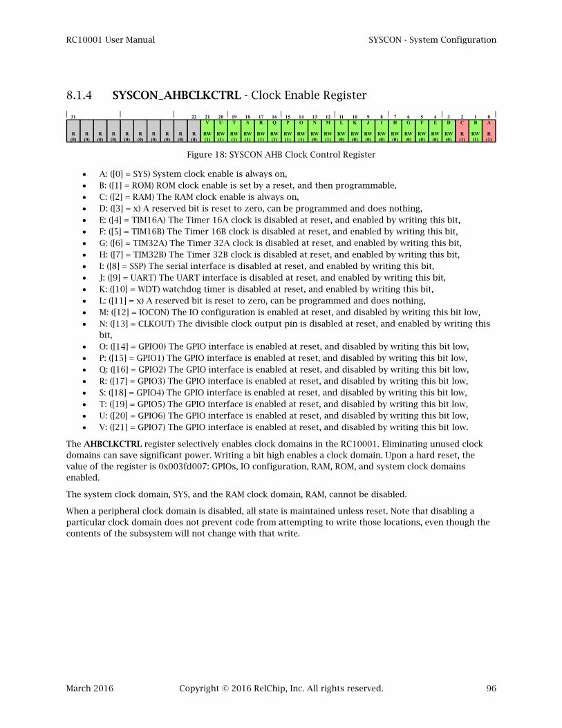
RC10001 User Manual SYSCON - System Configuration
March 2016 Copyright © 2016 RelChip, Inc. All rights reserved. 96
8.1.4 SYSCON_AHBCLKCTRL - Clock Enable Register
Figure 18: SYSCON AHB Clock Control Register
A: ([0] = SYS) System clock enable is always on, B: ([1] = ROM) ROM clock enable is set by a reset, and then programmable, C: ([2] = RAM) The RAM clock enable is always on, D: ([3] = x) A reserved bit is reset to zero, can be programmed and does nothing, E: ([4] = TIM16A) The Timer 16A clock is disabled at reset, and enabled by writing this bit, F: ([5] = TIM16B) The Timer 16B clock is disabled at reset, and enabled by writing this bit, G: ([6] = TIM32A) The Timer 32A clock is disabled at reset, and enabled by writing this bit, H: ([7] = TIM32B) The Timer 32B clock is disabled at reset, and enabled by writing this bit, I: ([8] = SSP) The serial interface is disabled at reset, and enabled by writing this bit, J: ([9] = UART) The UART interface is disabled at reset, and enabled by writing this bit, K: ([10] = WDT) watchdog timer is disabled at reset, and enabled by writing this bit, L: ([11] = x) A reserved bit is reset to zero, can be programmed and does nothing, M: ([12] = IOCON) The IO configuration is enabled at reset, and disabled by writing this bit low, N: ([13] = CLKOUT) The divisible clock output pin is disabled at reset, and enabled by writing this
bit, O: ([14] = GPIO0) The GPIO interface is enabled at reset, and disabled by writing this bit low, P: ([15] = GPIO1) The GPIO interface is enabled at reset, and disabled by writing this bit low, Q: ([16] = GPIO2) The GPIO interface is enabled at reset, and disabled by writing this bit low, R: ([17] = GPIO3) The GPIO interface is enabled at reset, and disabled by writing this bit low, S: ([18] = GPIO4) The GPIO interface is enabled at reset, and disabled by writing this bit low, T: ([19] = GPIO5) The GPIO interface is enabled at reset, and disabled by writing this bit low, U: ([20] = GPIO6) The GPIO interface is enabled at reset, and disabled by writing this bit low, V: ([21] = GPIO7) The GPIO interface is enabled at reset, and disabled by writing this bit low.
The AHBCLKCTRL register selectively enables clock domains in the RC10001. Eliminating unused clock domains can save significant power. Writing a bit high enables a clock domain. Upon a hard reset, the value of the register is 0x003fd007: GPIOs, IO configuration, RAM, ROM, and system clock domains enabled.
The system clock domain, SYS, and the RAM clock domain, RAM, cannot be disabled.
When a peripheral clock domain is disabled, all state is maintained unless reset. Note that disabling a particular clock domain does not prevent code from attempting to write those locations, even though the contents of the subsystem will not change with that write.
1B
RW(1)
R(0)
22
R(0)
2C
R(1)
0A
R(1)
3D
RW(0)
4E
RW(0)
5F
RW(0)
6G
RW(0)
7H
RW(0)
8I
RW(0)
9J
RW(0)
10K
RW(0)
11L
RW(0)
12M
RW(1)
13N
RW(0)
14O
RW(1)
15P
RW(1)
16Q
RW(1)
17R
RW(1)
18S
RW(1)
19T
RW(1)
20U
RW(1)
21V
RW(1)
R(0)
R(0)
R(0)
R(0)
31
R(0)
R(0)
R(0)
R(0)

RC10001 User Manual SYSCON - System Configuration
March 2016 Copyright © 2016 RelChip, Inc. All rights reserved. 97
8.1.5 SYSCON_AHBCLKDIV - System Clock Divisor Register
Figure 19: SYSCON System Clock Divisor Register
A: ([7:0] = DIV) Divisor.
The external (XTAL1) clock frequency is divided by this unsigned byte before driving any internal nodes. Valid values range from 1 to 255. The register resets to the value 1. Writing zero to this register is the same as writing a one.
8.1.6 SYSCON_CLKOUTDIV - Clock Output Pin Divisor Register
Figure 20: SYSCON Clock Output Pin Divisor Register
A: ([7:0] = DIV) Divisor.
The internal clock (after the system clock division) is divided by this unsigned byte, and applied to the CLKOUT pin. Programming this divisor to zero disables the clock.
8.1.7 SYSCON_SYSTCKCAL - System Tick Calibration Register
Figure 21: SYSCON System Tick Calibration Register
A: ([23:0] = CAL) The system tick timer loop count, B: ([24] = SKEW) A one indicates the clock division is inexact at 10ms. This is a function of the
calibration value and the system clock period.
The calibration register is a divisor for the System Tick Timer. The reset value is 0x0301_3880.
A
RW(0)
R(0)
A
RW(0)
A
RW(0)
A
RW(0)
A
RW(0)
7A
RW(0)
R(0)
R(0)
R(0)
R(0)
31
R(0)
R(0)
R(0)
R(0)
0A
RW(1)
A
RW(0)
R(0)
R(0)
R(0)
R(0)
R(0)
R(0)
R(0)
R(0)
R(0)
R(0)
R(0)
R(0)
R(0)
R(0)
8
R(0)
A
RW(0)
R(0)
A
RW(0)
A
RW(0)
A
RW(0)
A
RW(0)
7A
RW(0)
R(0)
R(0)
R(0)
R(0)
31
R(0)
R(0)
R(0)
R(0)
0A
RW(0)
A
RW(0)
R(0)
R(0)
R(0)
R(0)
R(0)
R(0)
R(0)
R(0)
R(0)
R(0)
R(0)
R(0)
R(0)
R(0)
8
R(0)
A
RW(0)
R(0)
A
RW(0)
A
RW(0)
A
RW(0)
A
RW(0)
A
RW(1)
R(0)
R(0)
R(0)
R(0)
31
R(0)
25
R(1)
0A
RW(0)
A
RW(0)
A
RW(0)
A
RW(0)
A
RW(0)
A
RW(1)
A
RW(1)
A
RW(1)
A
RW(0)
A
RW(0)
A
RW(1)
A
RW(0)
A
RW(0)
A
RW(0)
A
RW(0)
A
RW(0)
A
RW(0)
23A
RW(0)
24B
RW(1)

RC10001 User Manual SYSCON - System Configuration
March 2016 Copyright © 2016 RelChip, Inc. All rights reserved. 98
8.1.8 SYSCON_BATTCTRL - Battery Backup Control Register
Figure 22: SYSCON Battery Backup Control Register
A: ([0] = BBRE) Soft reset on battery backup enabled.
When the main power goes down on the integrated circuit, the battery backup power, if used, will keep the RAM contents correct. This register enables the battery backup circuit to assert a soft reset (BBRE = one). Thus, a boot sequence will not start when power returns, but a soft reset will occur.
8.1.9 SYSCON_DEVICEID - Device Identification Register
Figure 23: SYSCON Device Identification Register
A: ([15:0] = PARTNO) 0x2711 (10001 decimal) B: ([26:16] = JEDEC) 0x430 assigned to RelChip (four bit bank, and seven bit manufacturer’s
number) C: ([31:28] = VER) Version of the design
The part number, JEDEC manufacturer’s code, and version number are in this read-only register.
R(0)
R(0)
R(0)
R(0)
R(0)
31
R(0)
R(0)
0A
RW(0)
R(0)
R(0)
R(0)
R(0)
R(0)
R(0)
R(0)
R(0)
R(0)
R(0)
R(0)
R(0)
R(0)
R(0)
R(0)
R(0)
R(0)
R(0)
R(0)
R(0)
R(0)
R(0)
R(0)
1
R(0)
0A
R(1)
27
R(0)
A
R(0)
A
R(0)
A
R(0)
A
R(1)
A
R(0)
A
R(0)
A
R(0)
A
R(7)
A
R(1)
A
R(1)
A
R(0)
A
R(0)
A
R(1)
A
R(0)
15A
R(0)
16B
R(0)
B
R(0)
B
R(0)
B
R(0)
B
R(0)
B
R(0)
B
R(0)
B
R(0)
B
R(0)
B
R(0)
26B
R(0)
28C
R(1)
C
R(0)
C
R(0)
31C
R(0)

RC10001 User Manual NVIC - Nested Vectored Interrupt Controller
March 2016 Copyright © 2016 RelChip, Inc. All rights reserved. 99
9 NVIC - NESTED VECTORED INTERRUPT CONTROLLER
The RC10001 has six system exceptions/interrupts, and twenty-one peripheral interrupt sources. The NVIC provides enables and priorities for the peripheral interrupt sources. Multiple sources from each peripheral are possible, documented with the peripheral. The peripheral and NVIC both control enables, set pending and clear.
Exception and interrupt routine entry points are stored in the vector table beginning at address 0x0000_0000 (see Table 5).
Interrupt types (level, edge, etc.) are determined by peripheral register settings. Clearing interrupts is required before assertion of VECTCLRACTIVE in the SCB_AIRCR register. Otherwise, the interrupt will persist. Even when an interrupt is disabled, an interrupt will be generated and pending. However, until enabled, the pending interrupt will not cause a system reaction. The circuit samples the input to determine transitions on clock edges.
Programming the NVIC_ISER/NVIC_ISPR registers assert interrupts directly. The interrupts are cleared with a write to the NVIC_ICPR Register, but if the peripheral source is still driving an interrupt condition, this result is transitory and another interrupt will be generated. The interrupt service routine clears both NVIC and peripheral interrupts prior to exit.
9.1 INTERRUPT PRIORITY
Interrupts have a two-bit, four-level priority associated. The system interrupt priority for the three highest priority interrupts is constant (see Table 5). Other interrupt priorities are programmed into the NVIC_IPR# registers. 2b00 is the highest priority and 2b11 is the lowest.
9.2 SOFTWARE ASSERTION OF INTERRUPTS
Software can change an interrupt to pending, or clear the pending state by writing the pending registers. Clearing an interrupt with the Clear-Pending Register will not change an executing exception or interrupt.

RC10001 User Manual NVIC - Nested Vectored Interrupt Controller
March 2016 Copyright © 2016 RelChip, Inc. All rights reserved. 100
9.3 NVIC REGISTERS
Table 17: NVIC Register Map
Address Symbol Description
0xE000_E100 NVIC_ISER Interrupt Set-Enable
0xE000_E104 to 0xE000_E17F - Reserved
0xE000_E180 NVIC_ICER Interrupt Clear-Enable
0xE000_E184 to 0xE000_E1FF - Reserved
0xE000_E200 NVIC_ISPR Interrupt Set-Pending
0xE000_E204 to 0xE000_E27F - Reserved
0xE000_E280 NVIC_ICPR Interrupt Clear-Pending
0xE000_E284 to 0xE000_E3FF - Reserved
0xE000_E400 NVIC_IPR0 Interrupt Priority 0
0xE000_E404 NVIC_IPR1 Interrupt Priority 1
0xE000_E408 NVIC_IPR2 Interrupt Priority 2
0xE000_E40C NVIC_IPR3 Interrupt Priority 3
0xE000_E410 NVIC_IPR4 Interrupt Priority 4
0xE000_E414 NVIC_IPR5 Interrupt Priority 5
0xE000_E418 to 0xE000_ECFF - Reserved
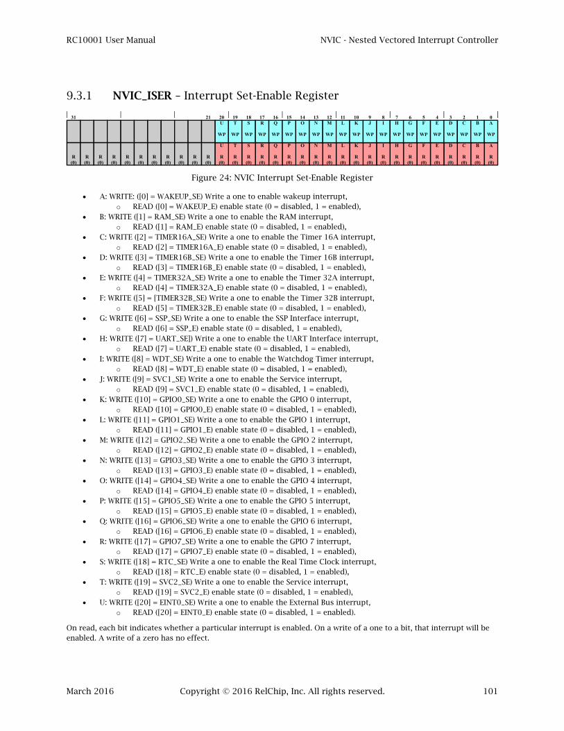
RC10001 User Manual NVIC - Nested Vectored Interrupt Controller
March 2016 Copyright © 2016 RelChip, Inc. All rights reserved. 101
9.3.1 NVIC_ISER – Interrupt Set-Enable Register
Figure 24: NVIC Interrupt Set-Enable Register
A: WRITE: ([0] = WAKEUP_SE) Write a one to enable wakeup interrupt, o READ ([0] = WAKEUP_E) enable state (0 = disabled, 1 = enabled),
B: WRITE ([1] = RAM_SE) Write a one to enable the RAM interrupt, o READ ([1] = RAM_E) enable state (0 = disabled, 1 = enabled),
C: WRITE ([2] = TIMER16A_SE) Write a one to enable the Timer 16A interrupt, o READ ([2] = TIMER16A_E) enable state (0 = disabled, 1 = enabled),
D: WRITE ([3] = TIMER16B_SE) Write a one to enable the Timer 16B interrupt, o READ ([3] = TIMER16B_E) enable state (0 = disabled, 1 = enabled),
E: WRITE ([4] = TIMER32A_SE) Write a one to enable the Timer 32A interrupt, o READ ([4] = TIMER32A_E) enable state (0 = disabled, 1 = enabled),
F: WRITE ([5] = [TIMER32B_SE) Write a one to enable the Timer 32B interrupt, o READ ([5] = TIMER32B_E) enable state (0 = disabled, 1 = enabled),
G: WRITE ([6] = SSP_SE) Write a one to enable the SSP Interface interrupt, o READ ([6] = SSP_E) enable state (0 = disabled, 1 = enabled),
H: WRITE ([7] = UART_SE]) Write a one to enable the UART Interface interrupt, o READ ([7] = UART_E) enable state (0 = disabled, 1 = enabled),
I: WRITE ([8] = WDT_SE) Write a one to enable the Watchdog Timer interrupt, o READ ([8] = WDT_E) enable state (0 = disabled, 1 = enabled),
J: WRITE ([9] = SVC1_SE) Write a one to enable the Service interrupt, o READ ([9] = SVC1_E) enable state (0 = disabled, 1 = enabled),
K: WRITE ([10] = GPIO0_SE) Write a one to enable the GPIO 0 interrupt, o READ ([10] = GPIO0_E) enable state (0 = disabled, 1 = enabled),
L: WRITE ([11] = GPIO1_SE) Write a one to enable the GPIO 1 interrupt, o READ ([11] = GPIO1_E) enable state (0 = disabled, 1 = enabled),
M: WRITE ([12] = GPIO2_SE) Write a one to enable the GPIO 2 interrupt, o READ ([12] = GPIO2_E) enable state (0 = disabled, 1 = enabled),
N: WRITE ([13] = GPIO3_SE) Write a one to enable the GPIO 3 interrupt, o READ ([13] = GPIO3_E) enable state (0 = disabled, 1 = enabled),
O: WRITE ([14] = GPIO4_SE) Write a one to enable the GPIO 4 interrupt, o READ ([14] = GPIO4_E) enable state (0 = disabled, 1 = enabled),
P: WRITE ([15] = GPIO5_SE) Write a one to enable the GPIO 5 interrupt, o READ ([15] = GPIO5_E) enable state (0 = disabled, 1 = enabled),
Q: WRITE ([16] = GPIO6_SE) Write a one to enable the GPIO 6 interrupt, o READ ([16] = GPIO6_E) enable state (0 = disabled, 1 = enabled),
R: WRITE ([17] = GPIO7_SE) Write a one to enable the GPIO 7 interrupt, o READ ([17] = GPIO7_E) enable state (0 = disabled, 1 = enabled),
S: WRITE ([18] = RTC_SE) Write a one to enable the Real Time Clock interrupt, o READ ([18] = RTC_E) enable state (0 = disabled, 1 = enabled),
T: WRITE ([19] = SVC2_SE) Write a one to enable the Service interrupt, o READ ([19] = SVC2_E) enable state (0 = disabled, 1 = enabled),
U: WRITE ([20] = EINT0_SE) Write a one to enable the External Bus interrupt, o READ ([20] = EINT0_E) enable state (0 = disabled, 1 = enabled).
On read, each bit indicates whether a particular interrupt is enabled. On a write of a one to a bit, that interrupt will be enabled. A write of a zero has no effect.
A
R(0)
B
R(0)
C
R(0)
D
R(0)
E
R(0)
F
R(0)
G
R(0)
H
R(0)
I
R(0)
J
R(0)
K
R(0)
L
R(0)
M
R(0)
N
R(0)
O
R(0)
P
R(0)
Q
R(0)
R
R(0)
S
R(0)
T
R(0)
U
R(0)
20U
WP
31
R(0)
R(0)
R(0)
R(0)
R(0)
R(0)
R(0)
R(0)
R(0)
R(0)
21
R(0)
19T
WP
18S
WP
17R
WP
16Q
WP
15P
WP
14O
WP
13N
WP
12M
WP
11L
WP
10K
WP
9J
WP
8I
WP
7H
WP
6G
WP
5F
WP
4E
WP
3D
WP
2C
WP
1B
WP
0A
WP

RC10001 User Manual NVIC - Nested Vectored Interrupt Controller
March 2016 Copyright © 2016 RelChip, Inc. All rights reserved. 102
9.3.2 NVIC_ICER – Interrupt Clear-Enable Register
Figure 25: NVIC Interrupt Clear-Enable Register
A: WRITE: ([0] = WAKEUP_CE) Write a one to disable wakeup interrupt, o READ ([0] = WAKEUP_E) enable state (0 = disabled, 1 = enabled),
B: WRITE ([1] = RAM_CE) Write a one to disable the RAM interrupt, o READ ([1] = RAM_E) enable state (0 = disabled, 1 = enabled),
C: WRITE ([2] = TIMER16A_CE) Write a one to disable the Timer 16A interrupt, o READ ([2] = TIMER16A_E) enable state (0 = disabled, 1 = enabled),
D: WRITE ([3] = TIMER16B_CE) Write a one to disable the Timer 16B interrupt, o READ ([3] = TIMER16B_E) enable state (0 = disabled, 1 = enabled),
E: WRITE ([4] = TIMER32A_CE) Write a one to disable the Timer 32A interrupt, o READ ([4] = TIMER32A_E) enable state (0 = disabled, 1 = enabled),
F: WRITE ([5] = [TIMER32B_CE) Write a one to disable the Timer 32B interrupt, o READ ([5] = TIMER32B_E) enable state (0 = disabled, 1 = enabled),
G: WRITE ([6] = SSP_CE) Write a one to disable the SSP Interface interrupt, o READ ([6] = SSP_E) enable state (0 = disabled, 1 = enabled),
H: WRITE ([7] = UART_CE]) Write a one to disable the UART Interface interrupt, o READ ([7] = UART_E) enable state (0 = disabled, 1 = enabled),
I: WRITE ([8] = WDT_CE) Write a one to disable the Watchdog Timer interrupt, o READ ([8] = WDT_E) enable state (0 = disabled, 1 = enabled),
J: WRITE ([9] = SVC1_CE) Write a one to disable the Service interrupt, o READ ([9] = SVC1_E) enable state (0 = disabled, 1 = enabled),
K: WRITE ([10] = GPIO0_CE) Write a one to disable the GPIO 0 interrupt, o READ ([10] = GPIO0_E) enable state (0 = disabled, 1 = enabled),
L: WRITE ([11] = GPIO1_CE) Write a one to disable the GPIO 1 interrupt, o READ ([11] = GPIO1_E) enable state (0 = disabled, 1 = enabled),
M: WRITE ([12] = GPIO2_CE) Write a one to disable the GPIO 2 interrupt, o READ ([12] = GPIO2_E) enable state (0 = disabled, 1 = enabled),
N: WRITE ([13] = GPIO3_CE) Write a one to disable the GPIO 3 interrupt, o READ ([13] = GPIO3_E) enable state (0 = disabled, 1 = enabled),
O: WRITE ([14] = GPIO4_CE) Write a one to disable the GPIO 4 interrupt, o READ ([14] = GPIO4_E) enable state (0 = disabled, 1 = enabled),
P: WRITE ([15] = GPIO5_CE) Write a one to disable the GPIO 5 interrupt, o READ ([15] = GPIO5_E) enable state (0 = disabled, 1 = enabled),
Q: WRITE ([16] = GPIO6_CE) Write a one to disable the GPIO 6 interrupt, o READ ([16] = GPIO6_E) enable state (0 = disabled, 1 = enabled),
R: WRITE ([17] = GPIO7_CE) Write a one to disable the GPIO 7 interrupt, o READ ([17] = GPIO7_E) enable state (0 = disabled, 1 = enabled),
S: WRITE ([18] = RTC_CE) Write a one to disable the Real Time Clock interrupt, o READ ([18] = RTC_E) enable state (0 = disabled, 1 = enabled),
T: WRITE ([19] = SVC2_CE) Write a one to disable the Service interrupt, o READ ([19] = SVC2_E) enable state (0 = disabled, 1 = enabled),
U: WRITE ([20] = EINT0_CE) Write a one to disable the External Bus interrupt, o READ ([20] = EINT0_E) enable state (0 = disabled, 1 = enabled).
On a read, each bit indicates whether a particular interrupt is enabled. On a write of a one to a bit, that interrupt will be disabled. A write of a zero has no effect.
A
R(0)
B
R(0)
C
R(0)
D
R(0)
E
R(0)
F
R(0)
G
R(0)
H
R(0)
I
R(0)
J
R(0)
K
R(0)
L
R(0)
M
R(0)
N
R(0)
O
R(0)
P
R(0)
Q
R(0)
R
R(0)
S
R(0)
T
R(0)
U
R(0)
20U
WP
31
R(0)
R(0)
R(0)
R(0)
R(0)
R(0)
R(0)
R(0)
R(0)
R(0)
21
R(0)
19T
WP
18S
WP
17R
WP
16Q
WP
15P
WP
14O
WP
13N
WP
12M
WP
11L
WP
10K
WP
9J
WP
8I
WP
7H
WP
6G
WP
5F
WP
4E
WP
3D
WP
2C
WP
1B
WP
0A
WP
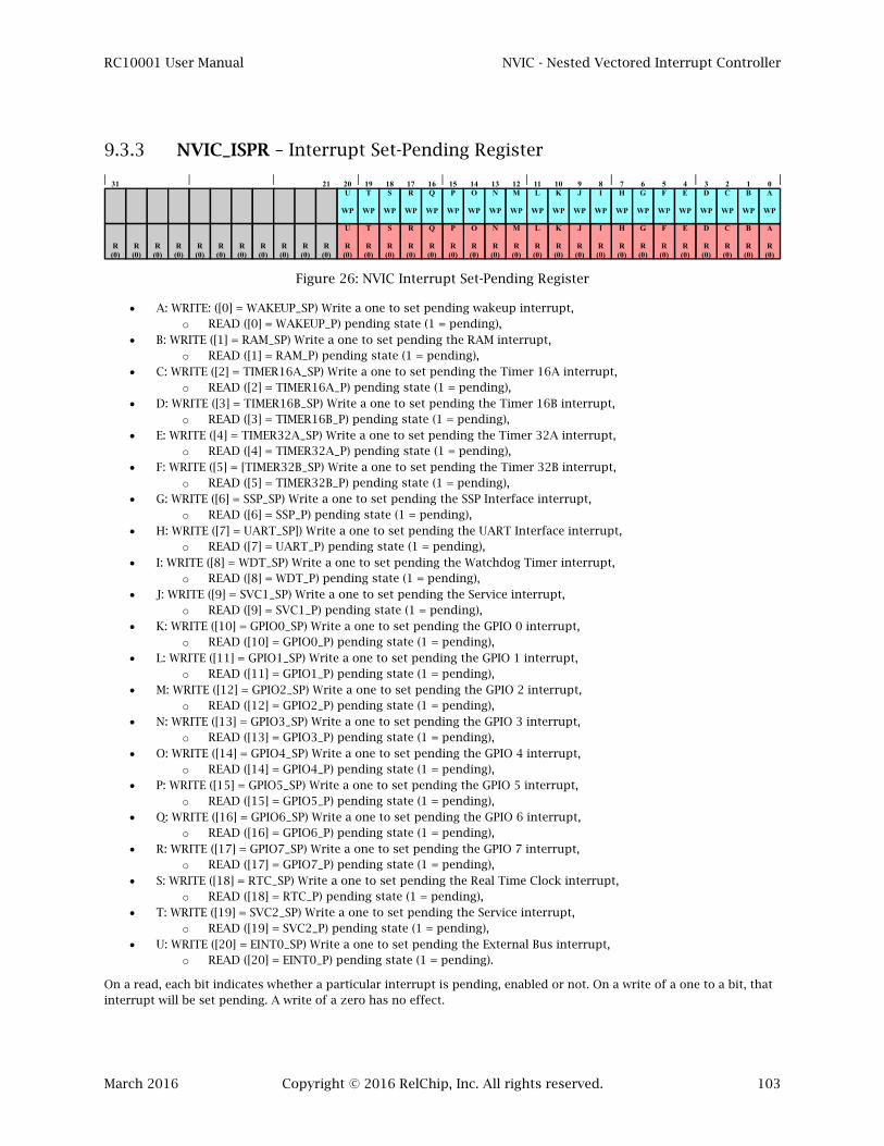
RC10001 User Manual NVIC - Nested Vectored Interrupt Controller
March 2016 Copyright © 2016 RelChip, Inc. All rights reserved. 103
9.3.3 NVIC_ISPR – Interrupt Set-Pending Register
Figure 26: NVIC Interrupt Set-Pending Register
A: WRITE: ([0] = WAKEUP_SP) Write a one to set pending wakeup interrupt, o READ ([0] = WAKEUP_P) pending state (1 = pending),
B: WRITE ([1] = RAM_SP) Write a one to set pending the RAM interrupt, o READ ([1] = RAM_P) pending state (1 = pending),
C: WRITE ([2] = TIMER16A_SP) Write a one to set pending the Timer 16A interrupt, o READ ([2] = TIMER16A_P) pending state (1 = pending),
D: WRITE ([3] = TIMER16B_SP) Write a one to set pending the Timer 16B interrupt, o READ ([3] = TIMER16B_P) pending state (1 = pending),
E: WRITE ([4] = TIMER32A_SP) Write a one to set pending the Timer 32A interrupt, o READ ([4] = TIMER32A_P) pending state (1 = pending),
F: WRITE ([5] = [TIMER32B_SP) Write a one to set pending the Timer 32B interrupt, o READ ([5] = TIMER32B_P) pending state (1 = pending),
G: WRITE ([6] = SSP_SP) Write a one to set pending the SSP Interface interrupt, o READ ([6] = SSP_P) pending state (1 = pending),
H: WRITE ([7] = UART_SP]) Write a one to set pending the UART Interface interrupt, o READ ([7] = UART_P) pending state (1 = pending),
I: WRITE ([8] = WDT_SP) Write a one to set pending the Watchdog Timer interrupt, o READ ([8] = WDT_P) pending state (1 = pending),
J: WRITE ([9] = SVC1_SP) Write a one to set pending the Service interrupt, o READ ([9] = SVC1_P) pending state (1 = pending),
K: WRITE ([10] = GPIO0_SP) Write a one to set pending the GPIO 0 interrupt, o READ ([10] = GPIO0_P) pending state (1 = pending),
L: WRITE ([11] = GPIO1_SP) Write a one to set pending the GPIO 1 interrupt, o READ ([11] = GPIO1_P) pending state (1 = pending),
M: WRITE ([12] = GPIO2_SP) Write a one to set pending the GPIO 2 interrupt, o READ ([12] = GPIO2_P) pending state (1 = pending),
N: WRITE ([13] = GPIO3_SP) Write a one to set pending the GPIO 3 interrupt, o READ ([13] = GPIO3_P) pending state (1 = pending),
O: WRITE ([14] = GPIO4_SP) Write a one to set pending the GPIO 4 interrupt, o READ ([14] = GPIO4_P) pending state (1 = pending),
P: WRITE ([15] = GPIO5_SP) Write a one to set pending the GPIO 5 interrupt, o READ ([15] = GPIO5_P) pending state (1 = pending),
Q: WRITE ([16] = GPIO6_SP) Write a one to set pending the GPIO 6 interrupt, o READ ([16] = GPIO6_P) pending state (1 = pending),
R: WRITE ([17] = GPIO7_SP) Write a one to set pending the GPIO 7 interrupt, o READ ([17] = GPIO7_P) pending state (1 = pending),
S: WRITE ([18] = RTC_SP) Write a one to set pending the Real Time Clock interrupt, o READ ([18] = RTC_P) pending state (1 = pending),
T: WRITE ([19] = SVC2_SP) Write a one to set pending the Service interrupt, o READ ([19] = SVC2_P) pending state (1 = pending),
U: WRITE ([20] = EINT0_SP) Write a one to set pending the External Bus interrupt, o READ ([20] = EINT0_P) pending state (1 = pending).
On a read, each bit indicates whether a particular interrupt is pending, enabled or not. On a write of a one to a bit, that interrupt will be set pending. A write of a zero has no effect.
A
R(0)
B
R(0)
C
R(0)
D
R(0)
E
R(0)
F
R(0)
G
R(0)
H
R(0)
I
R(0)
J
R(0)
K
R(0)
L
R(0)
M
R(0)
N
R(0)
O
R(0)
P
R(0)
Q
R(0)
R
R(0)
S
R(0)
T
R(0)
U
R(0)
20U
WP
31
R(0)
R(0)
R(0)
R(0)
R(0)
R(0)
R(0)
R(0)
R(0)
R(0)
21
R(0)
19T
WP
18S
WP
17R
WP
16Q
WP
15P
WP
14O
WP
13N
WP
12M
WP
11L
WP
10K
WP
9J
WP
8I
WP
7H
WP
6G
WP
5F
WP
4E
WP
3D
WP
2C
WP
1B
WP
0A
WP

RC10001 User Manual NVIC - Nested Vectored Interrupt Controller
March 2016 Copyright © 2016 RelChip, Inc. All rights reserved. 104
9.3.4 NVIC_ICPR – Interrupt Clear-Pending Register
Figure 27: NVIC Interrupt Clear-Pending Register
A: WRITE: ([0] = WAKEUP_SP) Write a one to clear pending wakeup interrupt, o READ ([0] = WAKEUP_P) pending state (1 = pending),
B: WRITE ([1] = RAM_SP) Write a one to clear pending the RAM interrupt, o READ ([1] = RAM_P) pending state (1 = pending),
C: WRITE ([2] = TIMER16A_SP) Write a one to clear pending the Timer 16A interrupt, o READ ([2] = TIMER16A_P) pending state (1 = pending),
D: WRITE ([3] = TIMER16B_SP) Write a one to clear pending the Timer 16B interrupt, o READ ([3] = TIMER16B_P) pending state (1 = pending),
E: WRITE ([4] = TIMER32A_SP) Write a one to clear pending the Timer 32A interrupt, o READ ([4] = TIMER32A_P) pending state (1 = pending),
F: WRITE ([5] = [TIMER32B_SP) Write a one to clear pending the Timer 32B interrupt, o READ ([5] = TIMER32B_P) pending state (1 = pending),
G: WRITE ([6] = SSP_SP) Write a one to clear pending the SSP Interface interrupt, o READ ([6] = SSP_P) pending state (1 = pending),
H: WRITE ([7] = UART_SP]) Write a one to clear pending the UART Interface interrupt, o READ ([7] = UART_P) pending state (1 = pending),
I: WRITE ([8] = WDT_SP) Write a one to clear pending the Watchdog Timer interrupt, o READ ([8] = WDT_P) pending state (1 = pending),
J: WRITE ([9] = SVC1_SP) Write a one to clear pending the Service interrupt, o READ ([9] = SVC1_P) pending state (1 = pending),
K: WRITE ([10] = GPIO0_SP) Write a one to clear pending the GPIO 0 interrupt, o READ ([10] = GPIO0_P) pending state (1 = pending),
L: WRITE ([11] = GPIO1_SP) Write a one to clear pending the GPIO 1 interrupt, o READ ([11] = GPIO1_P) pending state (1 = pending),
M: WRITE ([12] = GPIO2_SP) Write a one to clear pending the GPIO 2 interrupt, o READ ([12] = GPIO2_P) pending state (1 = pending),
N: WRITE ([13] = GPIO3_SP) Write a one to clear pending the GPIO 3 interrupt, o READ ([13] = GPIO3_P) pending state (1 = pending),
O: WRITE ([14] = GPIO4_SP) Write a one to clear pending the GPIO 4 interrupt, o READ ([14] = GPIO4_P) pending state (1 = pending),
P: WRITE ([15] = GPIO5_SP) Write a one to clear pending the GPIO 5 interrupt, o READ ([15] = GPIO5_P) pending state (1 = pending),
Q: WRITE ([16] = GPIO6_SP) Write a one to clear pending the GPIO 6 interrupt, o READ ([16] = GPIO6_P) pending state (1 = pending),
R: WRITE ([17] = GPIO7_SP) Write a one to clear pending the GPIO 7 interrupt, o READ ([17] = GPIO7_P) pending state (1 = pending),
S: WRITE ([18] = RTC_SP) Write a one to clear pending the Real Time Clock interrupt, o READ ([18] = RTC_P) pending state (1 = pending),
T: WRITE ([19] = SVC2_SP) Write a one to clear pending the Service interrupt, o READ ([19] = SVC2_P) pending state (1 = pending),
U: WRITE ([20] = EINT0_SP) Write a one to clear pending the External Bus interrupt, o READ ([20] = EINT0_P) pending state (1 = pending).
On a read, each bit indicates whether a particular interrupt is pending, enabled or not. On a write of a one to a bit, that interrupt will be set not pending. A write of a zero has no effect.
A
R(0)
B
R(0)
C
R(0)
D
R(0)
E
R(0)
F
R(0)
G
R(0)
H
R(0)
I
R(0)
J
R(0)
K
R(0)
L
R(0)
M
R(0)
N
R(0)
O
R(0)
P
R(0)
Q
R(0)
R
R(0)
S
R(0)
T
R(0)
U
R(0)
20U
WP
31
R(0)
R(0)
R(0)
R(0)
R(0)
R(0)
R(0)
R(0)
R(0)
R(0)
21
R(0)
19T
WP
18S
WP
17R
WP
16Q
WP
15P
WP
14O
WP
13N
WP
12M
WP
11L
WP
10K
WP
9J
WP
8I
WP
7H
WP
6G
WP
5F
WP
4E
WP
3D
WP
2C
WP
1B
WP
0A
WP
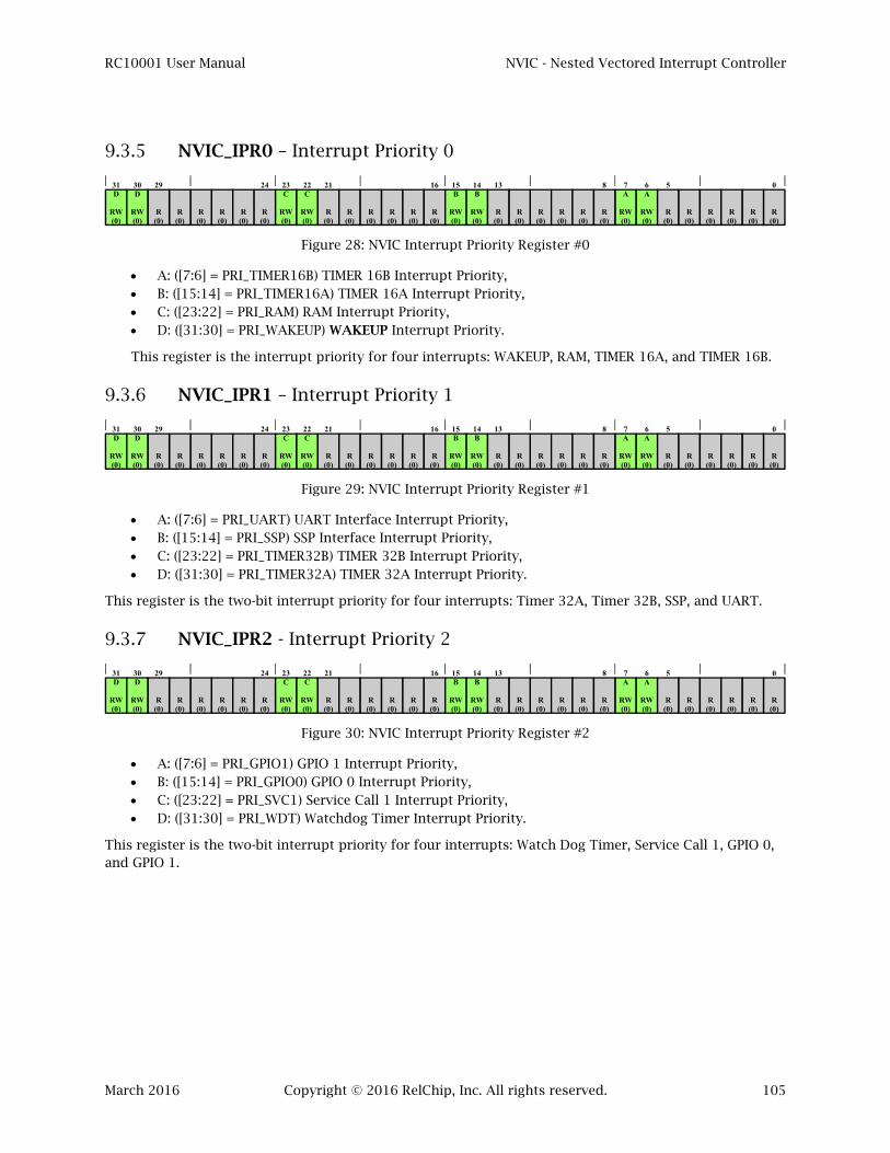
RC10001 User Manual NVIC - Nested Vectored Interrupt Controller
March 2016 Copyright © 2016 RelChip, Inc. All rights reserved. 105
9.3.5 NVIC_IPR0 – Interrupt Priority 0
Figure 28: NVIC Interrupt Priority Register #0
A: ([7:6] = PRI_TIMER16B) TIMER 16B Interrupt Priority, B: ([15:14] = PRI_TIMER16A) TIMER 16A Interrupt Priority, C: ([23:22] = PRI_RAM) RAM Interrupt Priority, D: ([31:30] = PRI_WAKEUP) WAKEUP Interrupt Priority.
This register is the interrupt priority for four interrupts: WAKEUP, RAM, TIMER 16A, and TIMER 16B.
9.3.6 NVIC_IPR1 – Interrupt Priority 1
Figure 29: NVIC Interrupt Priority Register #1
A: ([7:6] = PRI_UART) UART Interface Interrupt Priority, B: ([15:14] = PRI_SSP) SSP Interface Interrupt Priority, C: ([23:22] = PRI_TIMER32B) TIMER 32B Interrupt Priority, D: ([31:30] = PRI_TIMER32A) TIMER 32A Interrupt Priority.
This register is the two-bit interrupt priority for four interrupts: Timer 32A, Timer 32B, SSP, and UART.
9.3.7 NVIC_IPR2 - Interrupt Priority 2
Figure 30: NVIC Interrupt Priority Register #2
A: ([7:6] = PRI_GPIO1) GPIO 1 Interrupt Priority, B: ([15:14] = PRI_GPIO0) GPIO 0 Interrupt Priority, C: ([23:22] = PRI_SVC1) Service Call 1 Interrupt Priority, D: ([31:30] = PRI_WDT) Watchdog Timer Interrupt Priority.
This register is the two-bit interrupt priority for four interrupts: Watch Dog Timer, Service Call 1, GPIO 0, and GPIO 1.
31D
RW(0)
30D
RW(0)
23C
RW(0)
22C
RW(0)
R(0)
R(0)
R(0)
21
R(0)
R(0)
R(0)
R(0)
R(0)
16
R(0)
24
R(0)
R(0)
29
R(0)
15B
RW(0)
14B
RW(0)
7A
RW(0)
6A
RW(0)
R(0)
R(0)
R(0)
5
R(0)
R(0)
R(0)
R(0)
R(0)
0
R(0)
8
R(0)
R(0)
13
R(0)
31D
RW(0)
30D
RW(0)
23C
RW(0)
22C
RW(0)
R(0)
R(0)
R(0)
21
R(0)
R(0)
R(0)
R(0)
R(0)
16
R(0)
24
R(0)
R(0)
29
R(0)
15B
RW(0)
14B
RW(0)
7A
RW(0)
6A
RW(0)
R(0)
R(0)
R(0)
5
R(0)
R(0)
R(0)
R(0)
R(0)
0
R(0)
8
R(0)
R(0)
13
R(0)
31D
RW(0)
30D
RW(0)
23C
RW(0)
22C
RW(0)
R(0)
R(0)
R(0)
21
R(0)
R(0)
R(0)
R(0)
R(0)
16
R(0)
24
R(0)
R(0)
29
R(0)
15B
RW(0)
14B
RW(0)
7A
RW(0)
6A
RW(0)
R(0)
R(0)
R(0)
5
R(0)
R(0)
R(0)
R(0)
R(0)
0
R(0)
8
R(0)
R(0)
13
R(0)
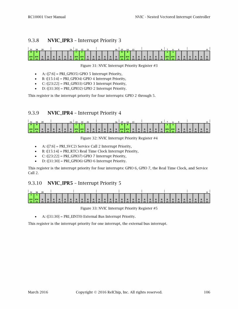
RC10001 User Manual NVIC - Nested Vectored Interrupt Controller
March 2016 Copyright © 2016 RelChip, Inc. All rights reserved. 106
9.3.8 NVIC_IPR3 – Interrupt Priority 3
Figure 31: NVIC Interrupt Priority Register #3
A: ([7:6] = PRI_GPIO5) GPIO 5 Interrupt Priority, B: ([15:14] = PRI_GPIO4) GPIO 4 Interrupt Priority, C: ([23:22] = PRI_GPIO3) GPIO 3 Interrupt Priority, D: ([31:30] = PRI_GPIO2) GPIO 2 Interrupt Priority.
This register is the interrupt priority for four interrupts: GPIO 2 through 5.
9.3.9 NVIC_IPR4 – Interrupt Priority 4
Figure 32: NVIC Interrupt Priority Register #4
A: ([7:6] = PRI_SVC2) Service Call 2 Interrupt Priority, B: ([15:14] = PRI_RTC) Real Time Clock Interrupt Priority, C: ([23:22] = PRI_GPIO7) GPIO 7 Interrupt Priority, D: ([31:30] = PRI_GPIO6) GPIO 6 Interrupt Priority.
This register is the interrupt priority for four interrupts: GPIO 6, GPIO 7, the Real Time Clock, and Service Call 2.
9.3.10 NVIC_IPR5 – Interrupt Priority 5
Figure 33: NVIC Interrupt Priority Register #5
A: ([31:30] = PRI_EINT0) External Bus Interrupt Priority.
This register is the interrupt priority for one interrupt, the external bus interrupt.
31D
RW(0)
30D
RW(0)
23C
RW(0)
22C
RW(0)
R(0)
R(0)
R(0)
21
R(0)
R(0)
R(0)
R(0)
R(0)
16
R(0)
24
R(0)
R(0)
29
R(0)
15B
RW(0)
14B
RW(0)
7A
RW(0)
6A
RW(0)
R(0)
R(0)
R(0)
5
R(0)
R(0)
R(0)
R(0)
R(0)
0
R(0)
8
R(0)
R(0)
13
R(0)
31D
RW(0)
30D
RW(0)
23C
RW(0)
22C
RW(0)
R(0)
R(0)
R(0)
21
R(0)
R(0)
R(0)
R(0)
R(0)
16
R(0)
24
R(0)
R(0)
29
R(0)
15B
RW(0)
14B
RW(0)
7A
RW(0)
6A
RW(0)
R(0)
R(0)
R(0)
5
R(0)
R(0)
R(0)
R(0)
R(0)
0
R(0)
8
R(0)
R(0)
13
R(0)
31A
RW(0)
30A
RW(0)
R(0)
R(0)
R(0)
R(0)
R(0)
R(0)
R(0)
R(0)
29
R(0)
R(0)
R(0)
R(0)
R(0)
R(0)
R(0)
R(0)
0
R(0)
R(0)
R(0)
R(0)
R(0)
R(0)
R(0)
R(0)
R(0)
R(0)
R(0)
R(0)
R(0)
R(0)
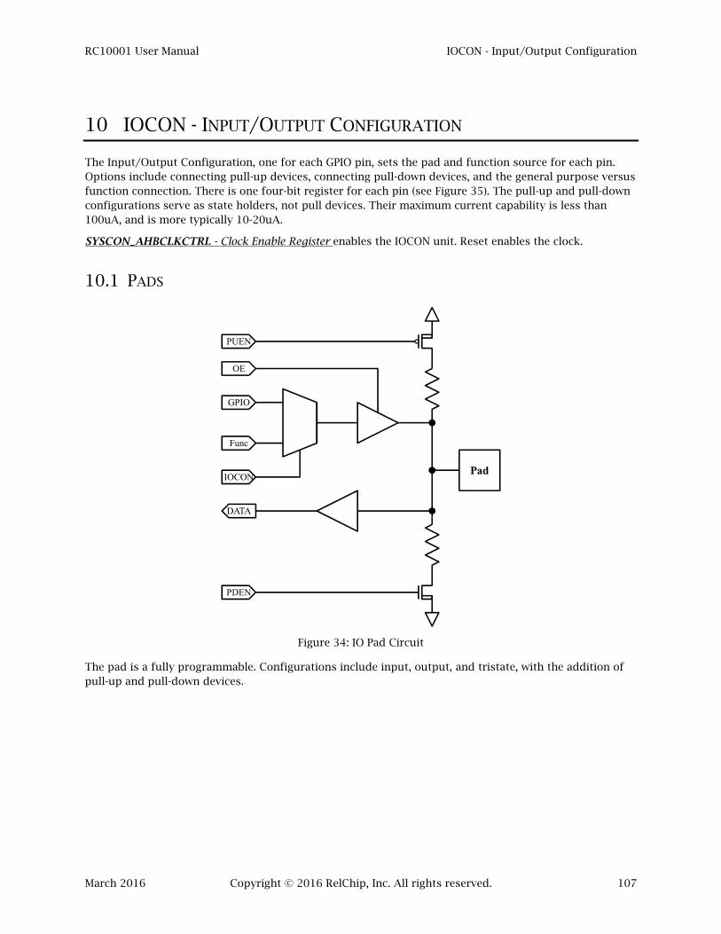
RC10001 User Manual IOCON - Input/Output Configuration
March 2016 Copyright © 2016 RelChip, Inc. All rights reserved. 107
10 IOCON - INPUT/OUTPUT CONFIGURATION
The Input/Output Configuration, one for each GPIO pin, sets the pad and function source for each pin. Options include connecting pull-up devices, connecting pull-down devices, and the general purpose versus function connection. There is one four-bit register for each pin (see Figure 35). The pull-up and pull-down configurations serve as state holders, not pull devices. Their maximum current capability is less than 100uA, and is more typically 10-20uA.
SYSCON_AHBCLKCTRL - Clock Enable Register enables the IOCON unit. Reset enables the clock.
10.1 PADS
Figure 34: IO Pad Circuit
The pad is a fully programmable. Configurations include input, output, and tristate, with the addition of pull-up and pull-down devices.
GPIO
Func
IOCON
OE
Pad
DATA
PUEN
PDEN

RC10001 User Manual IOCON - Input/Output Configuration
March 2016 Copyright © 2016 RelChip, Inc. All rights reserved. 108
10.2 REGISTERS
Figure 35: IOCON IO Configuration Register
A: ([0] = FUNC) Function (1) or GPIO (0) Connection to Data Input, Output, and Output Enable. B: ([1] = Reserved) Single Storage Bit, Reserved, C: ([3] = PUEN) Pull-Up Enable (High Active), D: ([4] = PDEN) Pull-Down Enable (High Active),
Each programmable IO pin has a register to configure the pin. While each register is an identical thirty-two bit register, each uses only three bits: FUNC, PDEN, and PUEN. Asserting FUNC (one) connects the pin to the internal function. A low FUNC connects the pin to the GPIO function. Table 18 through Table 25 show the register addresses.
PDEN and PUEN turn on the pull-down and pull-up enables respectively. There is no protection against turning them both on, causing a resistive connection between power and ground.
Table 18: SSP.TIMER16A/GPIO 0 IO Configuration Register Map
Pin/Register Access Address Reset
SCLK_GPIO0_0 RW 0x4004_4000 0x0000_0008
MISO_GPIO0_1 RW 0x4004_4004 0x0000_0008
MOSI_GPIO0_2 RW 0x4004_4008 0x0000_0008
SSELA_GPIO0_3 RW 0x4004_400C 0x0000_0008
SSELB_GPIO0_4 RW 0x4004_4010 0x0000_0008
SSELC_GPIO0_5 RW 0x4004_4014 0x0000_0008
SSELD_GPIO0_6 RW 0x4004_4018 0x0000_0008
T16ACAP0_GPIO0_7 RW 0x4004_401C 0x0000_0008
T16AMAT0_GPIO0_8 RW 0x4004_4020 0x0000_0008
T16AMAT1_GPIO0_9 RW 0x4004_4024 0x0000_0008
T16AMAT2_GPIO0_10 RW 0x4004_4028 0x0000_0008
T16AMAT3_GPIO0_11 RW 0x4004_402C 0x0000_0008
1B
RW(0)
0A
RW(0)
R(0)
R(0)
R(0)
R(0)
R(0)
R(0)
R(0)
R(0)
R(0)
R(0)
R(0)
R(0)
2
R(0)
R(0)
R(0)
R(0)
R(0)
R(0)
R(0)
R(0)
R(0)
R(0)
R(0)
R(0)
R(0)
5
R(0)
R(0)
31
R(0)
4D
RW(0)
3C
RW(0)

RC10001 User Manual IOCON - Input/Output Configuration
March 2016 Copyright © 2016 RelChip, Inc. All rights reserved. 109
Table 19: TIMER16B/TIMER32A/TIMER32B/GPIO 1 IO Configuration Register Map
Pin/Register Access Address Reset
T16BCAP0_GPIO1_0 RW 0x4004_4030 0x0000_0008
T16BMAT0_GPIO1_1 RW 0x4004_4034 0x0000_0008
T16BMAT1_GPIO1_2 RW 0x4004_4038 0x0000_0008
T16BMAT2_GPIO1_3 RW 0x4004_403C 0x0000_0008
T16BMAT3_GPIO1_4 RW 0x4004_4040 0x0000_0008
T32ACAP0_GPIO1_5 RW 0x4004_4044 0x0000_0008
T32AMAT0_GPIO1_6 RW 0x4004_4048 0x0000_0008
T32AMAT1_GPIO1_7 RW 0x4004_404C 0x0000_0008
T32AMAT2_GPIO1_8 RW 0x4004_4050 0x0000_0008
T32AMAT3_GPIO1_9 RW 0x4004_4054 0x0000_0008
T32BCAP0_GPIO1_10 RW 0x4004_4058 0x0000_0008
T32BMAT0_GPIO1_11 RW 0x4004_405C 0x0000_0008
Table 20: TIMER32B/UART/GPIO 2 IO Configuration Register Map
Pin/Register Access Address Reset
T32BMAT1_GPIO2_0 RW 0x4004_4060 0x0000_0008
T32BMAT2_GPIO2_1 RW 0x4004_4064 0x0000_0008
T32BMAT3_GPIO2_2 RW 0x4004_4068 0x0000_0008
RXD_GPIO2_3 RW 0x4004_406C 0x0000_0008
TXD_GPIO2_4 RW 0x4004_4070 0x0000_0008
CTSN_GPIO2_5 RW 0x4004_4074 0x0000_0008
DSRN_GPIO2_6 RW 0x4004_4078 0x0000_0008
RIN_GPIO2_7 RW 0x4004_407C 0x0000_0008
DCDN_GPIO2_8 RW 0x4004_4080 0x0000_0008
RTSN_GPIO2_9 RW 0x4004_4084 0x0000_0008
DTRN_GPIO2_10 RW 0x4004_4088 0x0000_0008
OUT1_GPIO2_11 RW 0x4004_408C 0x0000_0008
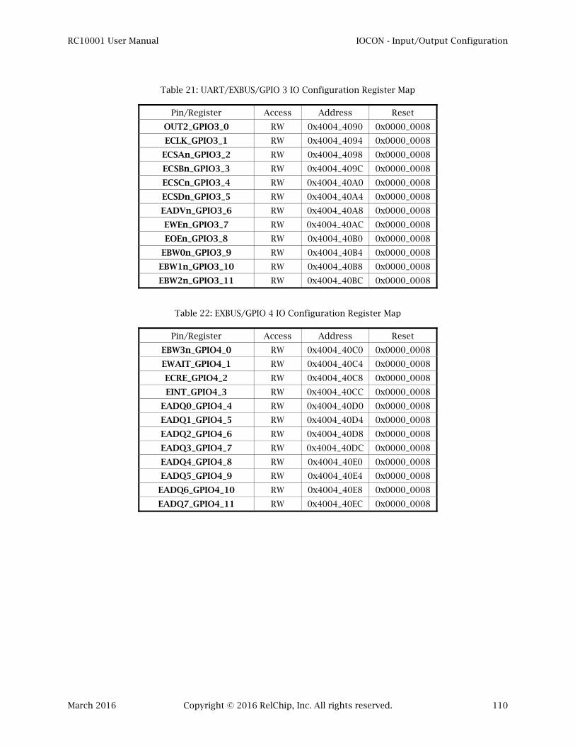
RC10001 User Manual IOCON - Input/Output Configuration
March 2016 Copyright © 2016 RelChip, Inc. All rights reserved. 110
Table 21: UART/EXBUS/GPIO 3 IO Configuration Register Map
Pin/Register Access Address Reset
OUT2_GPIO3_0 RW 0x4004_4090 0x0000_0008
ECLK_GPIO3_1 RW 0x4004_4094 0x0000_0008
ECSAn_GPIO3_2 RW 0x4004_4098 0x0000_0008
ECSBn_GPIO3_3 RW 0x4004_409C 0x0000_0008
ECSCn_GPIO3_4 RW 0x4004_40A0 0x0000_0008
ECSDn_GPIO3_5 RW 0x4004_40A4 0x0000_0008
EADVn_GPIO3_6 RW 0x4004_40A8 0x0000_0008
EWEn_GPIO3_7 RW 0x4004_40AC 0x0000_0008
EOEn_GPIO3_8 RW 0x4004_40B0 0x0000_0008
EBW0n_GPIO3_9 RW 0x4004_40B4 0x0000_0008
EBW1n_GPIO3_10 RW 0x4004_40B8 0x0000_0008
EBW2n_GPIO3_11 RW 0x4004_40BC 0x0000_0008
Table 22: EXBUS/GPIO 4 IO Configuration Register Map
Pin/Register Access Address Reset
EBW3n_GPIO4_0 RW 0x4004_40C0 0x0000_0008
EWAIT_GPIO4_1 RW 0x4004_40C4 0x0000_0008
ECRE_GPIO4_2 RW 0x4004_40C8 0x0000_0008
EINT_GPIO4_3 RW 0x4004_40CC 0x0000_0008
EADQ0_GPIO4_4 RW 0x4004_40D0 0x0000_0008
EADQ1_GPIO4_5 RW 0x4004_40D4 0x0000_0008
EADQ2_GPIO4_6 RW 0x4004_40D8 0x0000_0008
EADQ3_GPIO4_7 RW 0x4004_40DC 0x0000_0008
EADQ4_GPIO4_8 RW 0x4004_40E0 0x0000_0008
EADQ5_GPIO4_9 RW 0x4004_40E4 0x0000_0008
EADQ6_GPIO4_10 RW 0x4004_40E8 0x0000_0008
EADQ7_GPIO4_11 RW 0x4004_40EC 0x0000_0008
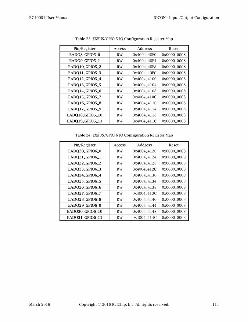
RC10001 User Manual IOCON - Input/Output Configuration
March 2016 Copyright © 2016 RelChip, Inc. All rights reserved. 111
Table 23: EXBUS/GPIO 5 IO Configuration Register Map
Pin/Register Access Address Reset
EADQ8_GPIO5_0 RW 0x4004_40F0 0x0000_0008
EADQ9_GPIO5_1 RW 0x4004_40F4 0x0000_0008
EADQ10_GPIO5_2 RW 0x4004_40F8 0x0000_0008
EADQ11_GPIO5_3 RW 0x4004_40FC 0x0000_0008
EADQ12_GPIO5_4 RW 0x4004_4100 0x0000_0008
EADQ13_GPIO5_5 RW 0x4004_4104 0x0000_0008
EADQ14_GPIO5_6 RW 0x4004_4108 0x0000_0008
EADQ15_GPIO5_7 RW 0x4004_410C 0x0000_0008
EADQ16_GPIO5_8 RW 0x4004_4110 0x0000_0008
EADQ17_GPIO5_9 RW 0x4004_4114 0x0000_0008
EADQ18_GPIO5_10 RW 0x4004_4118 0x0000_0008
EADQ19_GPIO5_11 RW 0x4004_411C 0x0000_0008
Table 24: EXBUS/GPIO 6 IO Configuration Register Map
Pin/Register Access Address Reset
EADQ20_GPIO6_0 RW 0x4004_4120 0x0000_0008
EADQ21_GPIO6_1 RW 0x4004_4124 0x0000_0008
EADQ22_GPIO6_2 RW 0x4004_4128 0x0000_0008
EADQ23_GPIO6_3 RW 0x4004_412C 0x0000_0008
EADQ24_GPIO6_4 RW 0x4004_4130 0x0000_0008
EADQ25_GPIO6_5 RW 0x4004_4134 0x0000_0008
EADQ26_GPIO6_6 RW 0x4004_4138 0x0000_0008
EADQ27_GPIO6_7 RW 0x4004_413C 0x0000_0008
EADQ28_GPIO6_8 RW 0x4004_4140 0x0000_0008
EADQ29_GPIO6_9 RW 0x4004_4144 0x0000_0008
EADQ30_GPIO6_10 RW 0x4004_4148 0x0000_0008
EADQ31_GPIO6_11 RW 0x4004_414C 0x0000_0008

RC10001 User Manual IOCON - Input/Output Configuration
March 2016 Copyright © 2016 RelChip, Inc. All rights reserved. 112
Table 25: EXBUS/SWD/GPIO 7 IO Configuration Register Map
Pin/Register Access Address Reset
EPDQ0_GPIO7_0 RW 0x4004_4150 0x0000_0008
EPDQ1_GPIO7_1 RW 0x4004_4154 0x0000_0008
EPDQ2_GPIO7_2 RW 0x4004_4158 0x0000_0008
EPDQ3_GPIO7_3 RW 0x4004_415C 0x0000_0008
SWCLK_GPIO7_4 RW 0x4004_4160 0x0000_0009
SWDIO_GPIO7_5 RW 0x4004_4164 0x0000_0009

RC10001 User Manual GPIO - General Purpose Input/Output Ports
March 2016 Copyright © 2016 RelChip, Inc. All rights reserved. 113
11 GPIO - GENERAL PURPOSE INPUT/OUTPUT PORTS
There are ninety general-purpose input/output (GPIO) pins available on the RC10001. There are eight groups of GPIO pins: GPIO 0 through 6 are 12 bits wide, and GPIO 7 is six bits wide. SYSCON_AHBCLKCTRL - Clock Enable Register enables the clock domain for each group of GPIO pins. Reset enables all GPIO clock domains.
All RC10001 pins are named “<function>_GPIO<groupNumber>_<index>”. <Function> is the pin name for the alternate function. Group number is 0 through 7. The index ranges from 0 to 11 (GPIO 7 only indexes from 0 to 5).
A different address space exists for each GPIO group (see Table 28).
11.1 OPERATION
The GPIO registers control the direction, logic value, and interrupt input state of each of the GPIO pins. All GPIO Pins:
Can Be Configured as Input or Output (or switched during program operation); Default (reset) to Input with Pull-Ups, except GPIO7_4 and GPIO7_5 which default to the serial
wire debug function with Pull-Ups; Can be either an Edge or Level Sensitive Interrupt Input. Edge Triggers can be rising, falling or on
both edges. Level Triggers can be either high or low active; Mask Read and Write Data with Address Bits 13 through 2.
11.1.1 Masked Write
The address ([13:2]) masks the twelve bits written by a GPIO data write. This insures no runt pulses can occur on other GPIO outputs in a group. It also allows complete pin-by-pin control of an operation.
The write operation, shown in Table 26, ignores bits that are set as function in the IOCON registers (bits 0 and 1 in this example), and bits that are set to read (bits 2, 3, and 6 through 8). The remaining bits are written if the appropriate mask bit is set (addresses 2 through 13 for data bits 0 through 11). In this example, bits 5, 10, and 11 are written with new data, while bits 4 and 9 will be masked.
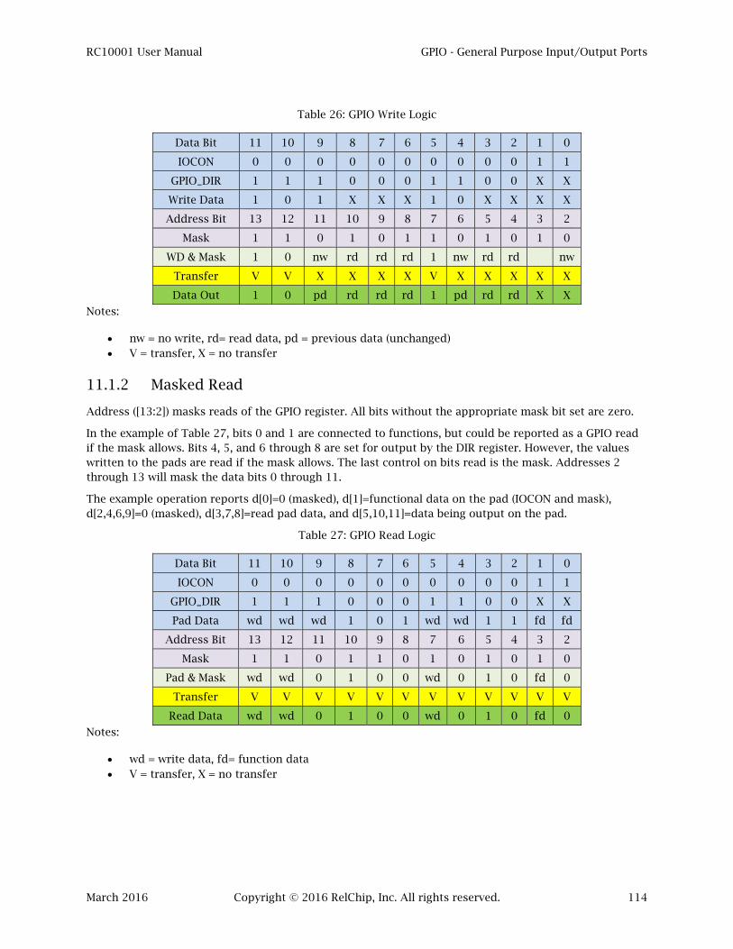
RC10001 User Manual GPIO - General Purpose Input/Output Ports
March 2016 Copyright © 2016 RelChip, Inc. All rights reserved. 114
Table 26: GPIO Write Logic
Data Bit 11 10 9 8 7 6 5 4 3 2 1 0
IOCON 0 0 0 0 0 0 0 0 0 0 1 1
GPIO_DIR 1 1 1 0 0 0 1 1 0 0 X X
Write Data 1 0 1 X X X 1 0 X X X X
Address Bit 13 12 11 10 9 8 7 6 5 4 3 2
Mask 1 1 0 1 0 1 1 0 1 0 1 0
WD & Mask 1 0 nw rd rd rd 1 nw rd rd nw
Transfer V V X X X X V X X X X X
Data Out 1 0 pd rd rd rd 1 pd rd rd X X
Notes:
nw = no write, rd= read data, pd = previous data (unchanged) V = transfer, X = no transfer
11.1.2 Masked Read
Address ([13:2]) masks reads of the GPIO register. All bits without the appropriate mask bit set are zero.
In the example of Table 27, bits 0 and 1 are connected to functions, but could be reported as a GPIO read if the mask allows. Bits 4, 5, and 6 through 8 are set for output by the DIR register. However, the values written to the pads are read if the mask allows. The last control on bits read is the mask. Addresses 2 through 13 will mask the data bits 0 through 11.
The example operation reports d[0]=0 (masked), d[1]=functional data on the pad (IOCON and mask), d[2,4,6,9]=0 (masked), d[3,7,8]=read pad data, and d[5,10,11]=data being output on the pad.
Table 27: GPIO Read Logic
Data Bit 11 10 9 8 7 6 5 4 3 2 1 0
IOCON 0 0 0 0 0 0 0 0 0 0 1 1
GPIO_DIR 1 1 1 0 0 0 1 1 0 0 X X
Pad Data wd wd wd 1 0 1 wd wd 1 1 fd fd
Address Bit 13 12 11 10 9 8 7 6 5 4 3 2
Mask 1 1 0 1 1 0 1 0 1 0 1 0
Pad & Mask wd wd 0 1 0 0 wd 0 1 0 fd 0
Transfer V V V V V V V V V V V V
Read Data wd wd 0 1 0 0 wd 0 1 0 fd 0
Notes:
wd = write data, fd= function data V = transfer, X = no transfer
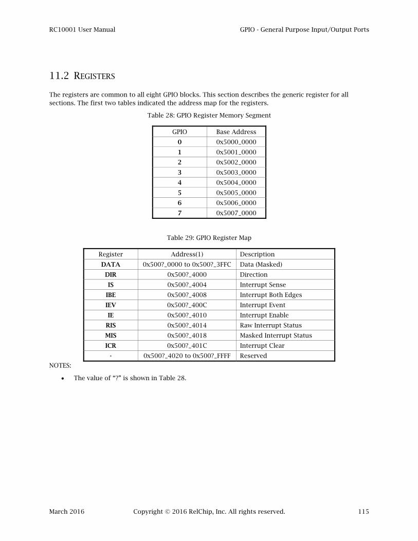
RC10001 User Manual GPIO - General Purpose Input/Output Ports
March 2016 Copyright © 2016 RelChip, Inc. All rights reserved. 115
11.2 REGISTERS
The registers are common to all eight GPIO blocks. This section describes the generic register for all sections. The first two tables indicated the address map for the registers.
Table 28: GPIO Register Memory Segment
GPIO Base Address
0 0x5000_0000
1 0x5001_0000
2 0x5002_0000
3 0x5003_0000
4 0x5004_0000
5 0x5005_0000
6 0x5006_0000
7 0x5007_0000
Table 29: GPIO Register Map
Register Address(1) Description
DATA 0x500?_0000 to 0x500?_3FFC Data (Masked)
DIR 0x500?_4000 Direction
IS 0x500?_4004 Interrupt Sense
IBE 0x500?_4008 Interrupt Both Edges
IEV 0x500?_400C Interrupt Event
IE 0x500?_4010 Interrupt Enable
RIS 0x500?_4014 Raw Interrupt Status
MIS 0x500?_4018 Masked Interrupt Status
ICR 0x500?_401C Interrupt Clear
- 0x500?_4020 to 0x500?_FFFF Reserved
NOTES:
The value of “?” is shown in Table 28.

RC10001 User Manual GPIO - General Purpose Input/Output Ports
March 2016 Copyright © 2016 RelChip, Inc. All rights reserved. 116
11.2.1 GPIO_DATA - Masked Data Register
Figure 36: GPIO Masked Data Register (GPIO0 to GPIO6)
A: ([11:0] = DATA) Data Field (can be bit masked on either a read or write).
Figure 37: GPIO 7 Masked Data Register
A: ([5:0] = DATA) Data Field (can be bit masked on either a read or write), B: ([7:6] = BOOT_SEL) Input only fields from BOOT_SEL1 and BOOT_SEL0 respectively.
There are seven twelve-bit GPIO_DATA registers (GPIO0 through 6) and one eight-bit GPIO_DATA register (GPIO7). Data is read or written as masked by addresses [13:2] (see Masked Write and Masked Read). GPIO 7 includes two input only bits connected to the boot selection pins. Note input and output are stored in the same physical register. Thus, when switching a GPIO bit from input to output, the value previously on the pin will be the initial value output. A GPIO_DATA read while a bit is in output mode reads the output value.
11.2.2 GPIO_DIR - Direction Register
Figure 38: GPIO Direction Register (GPIO 0 to 6)
A: ([11:0] = DIR) Direction for each pin in GPIO mode, 0 for input and 1 for output.
Figure 39: GPIO 7 Direction Register
A: ([5:0] = DIR) Direction for each pin in GPIO mode, 0 for input and 1 for output.
There are seven twelve-bit direction registers (GPIO0 through 6) and one six-bit direction register (GPIO7). Each bit controls the input (0) or output (1) direction of the associated GPIO pin.
A
RW(X)
R(0)
A
RW(X)
A
RW(X)
A
RW(X)
A
RW(X)
A
RW(X)
R(0)
R(0)
R(0)
R(0)
31
R(0)
R(0)
0A
RW(X)
A
RW(X)
A
RW(X)
A
RW(X)
A
RW(X)
11A
RW(X)
R(0)
R(0)
R(0)
R(0)
R(0)
R(0)
R(0)
R(0)
R(0)
R(0)
R(0)
R(0)
12
R(0)
A
RW(X)
R(0)
A
RW(X)
A
RW(X)
5A
RW(X)
R(0)
R(0)
R(0)
R(0)
31
R(0)
R(0)
0A
RW(X)
A
RW(X)
R(0)
R(0)
R(0)
R(0)
R(0)
R(0)
R(0)
R(0)
R(0)
R(0)
R(0)
R(0)
7B
R(X)
R(0)
R(0)
R(0)
R(0)
8
R(0)
6B
R(X)
A
RW(0)
R(0)
A
RW(0)
A
RW(0)
A
RW(0)
A
RW(0)
A
RW(0)
R(0)
R(0)
R(0)
R(0)
31
R(0)
R(0)
0A
RW(0)
A
RW(0)
A
RW(0)
A
RW(0)
A
RW(0)
11A
RW(0)
R(0)
R(0)
R(0)
R(0)
R(0)
R(0)
R(0)
R(0)
R(0)
R(0)
R(0)
R(0)
12
R(0)
A
RW(0)
R(0)
A
RW(0)
A
RW(0)
5A
RW(0)
R(0)
R(0)
R(0)
R(0)
31
R(0)
R(0)
0A
RW(0)
A
RW(0)
R(0)
R(0)
R(0)
R(0)
R(0)
R(0)
R(0)
R(0)
R(0)
R(0)
R(0)
R(0)
R(0)
R(0)
R(0)
R(0)
R(0)
R(0)
6
R(0)

RC10001 User Manual GPIO - General Purpose Input/Output Ports
March 2016 Copyright © 2016 RelChip, Inc. All rights reserved. 117
11.2.3 GPIO_IS – Interrupt Sense Register
Figure 40: GPIO Interrupt Sense Register (GPIO 0 to 6)
A: ([11:0] = IS) Selects edge or level sensitive interrupts per pin.
Figure 41: GPIO 7 Interrupt Sense Register
A: ([5:0] = IS) Selects edge or level sensitive interrupts per pin.
There are seven twelve-bit sense registers (GPIO0 through 6) and one six-bit sense register (GPIO7). Each bit controls a single pin. Options for each pin include zero for edge sensitive interrupts, and one for level sensitive interrupts. The system clock edge samples the input to set an interrupt (both edge and level). The sampled value determines a level sensitive interrupt, while the last two samples determine an edge sensitive interrupt. The GPIO_ICR register clears interrupts.
11.2.4 GPIO_IBE – Interrupt Both Edges Register
Figure 42: GPIO Interrupt Both Edges Register (GPIO 0 to 6)
A: ([11:0] = IBE) Sets both edges for edge sensitive interrupts per pin.
Figure 43: GPIO 7 Interrupt Both Edges Register
A: ([5:0] = IBE) Sets both edges for edge sensitive interrupts per pin.
There are seven twelve-bit interrupt registers (GPIO0 through 6) and one six-bit interrupt register (GPIO7). Interrupts will occur on both edges if the appropriate bit is set in this register, and the IS register is set to edge interrupt.
A
RW(0)
R(0)
A
RW(0)
A
RW(0)
A
RW(0)
A
RW(0)
A
RW(0)
R(0)
R(0)
R(0)
R(0)
31
R(0)
R(0)
0A
RW(0)
A
RW(0)
A
RW(0)
A
RW(0)
A
RW(0)
11A
RW(0)
R(0)
R(0)
R(0)
R(0)
R(0)
R(0)
R(0)
R(0)
R(0)
R(0)
R(0)
R(0)
12
R(0)
A
RW(0)
R(0)
A
RW(0)
A
RW(0)
5A
RW(0)
R(0)
R(0)
R(0)
R(0)
31
R(0)
R(0)
0A
RW(0)
A
RW(0)
R(0)
R(0)
R(0)
R(0)
R(0)
R(0)
R(0)
R(0)
R(0)
R(0)
R(0)
R(0)
R(0)
R(0)
R(0)
R(0)
R(0)
R(0)
6
R(0)
A
RW(0)
R(0)
A
RW(0)
A
RW(0)
A
RW(0)
A
RW(0)
A
RW(0)
R(0)
R(0)
R(0)
R(0)
31
R(0)
R(0)
0A
RW(0)
A
RW(0)
A
RW(0)
A
RW(0)
A
RW(0)
11A
RW(0)
R(0)
R(0)
R(0)
R(0)
R(0)
R(0)
R(0)
R(0)
R(0)
R(0)
R(0)
R(0)
12
R(0)
A
RW(0)
R(0)
A
RW(0)
A
RW(0)
5A
RW(0)
R(0)
R(0)
R(0)
R(0)
31
R(0)
R(0)
0A
RW(0)
A
RW(0)
R(0)
R(0)
R(0)
R(0)
R(0)
R(0)
R(0)
R(0)
R(0)
R(0)
R(0)
R(0)
R(0)
R(0)
R(0)
R(0)
R(0)
R(0)
6
R(0)
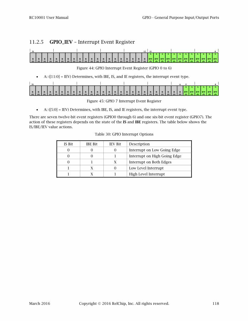
RC10001 User Manual GPIO - General Purpose Input/Output Ports
March 2016 Copyright © 2016 RelChip, Inc. All rights reserved. 118
11.2.5 GPIO_IEV – Interrupt Event Register
Figure 44: GPIO Interrupt Event Register (GPIO 0 to 6)
A: ([11:0] = IEV) Determines, with IBE, IS, and IE registers, the interrupt event type.
Figure 45: GPIO 7 Interrupt Event Register
A: ([5:0] = IEV) Determines, with IBE, IS, and IE registers, the interrupt event type.
There are seven twelve-bit event registers (GPIO0 through 6) and one six-bit event register (GPIO7). The action of these registers depends on the state of the IS and IBE registers. The table below shows the IS/IBE/IEV value actions.
Table 30: GPIO Interrupt Options
IS Bit IBE Bit IEV Bit Description
0 0 0 Interrupt on Low Going Edge
0 0 1 Interrupt on High Going Edge
0 1 X Interrupt on Both Edges
1 X 0 Low Level Interrupt
1 X 1 High Level Interrupt
A
RW(0)
R(0)
A
RW(0)
A
RW(0)
A
RW(0)
A
RW(0)
A
RW(0)
R(0)
R(0)
R(0)
R(0)
31
R(0)
R(0)
0A
RW(0)
A
RW(0)
A
RW(0)
A
RW(0)
A
RW(0)
11A
RW(0)
R(0)
R(0)
R(0)
R(0)
R(0)
R(0)
R(0)
R(0)
R(0)
R(0)
R(0)
R(0)
12
R(0)
A
RW(0)
R(0)
A
RW(0)
A
RW(0)
5A
RW(0)
R(0)
R(0)
R(0)
R(0)
31
R(0)
R(0)
0A
RW(0)
A
RW(0)
R(0)
R(0)
R(0)
R(0)
R(0)
R(0)
R(0)
R(0)
R(0)
R(0)
R(0)
R(0)
R(0)
R(0)
R(0)
R(0)
R(0)
R(0)
6
R(0)
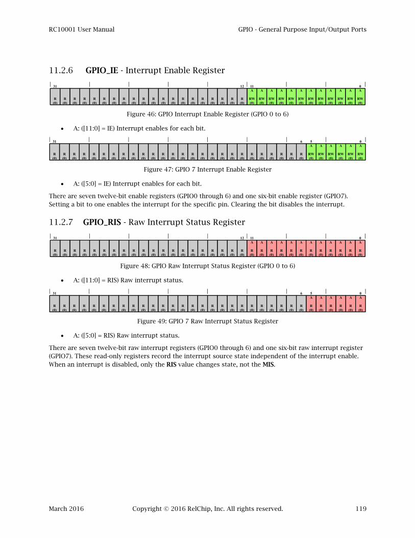
RC10001 User Manual GPIO - General Purpose Input/Output Ports
March 2016 Copyright © 2016 RelChip, Inc. All rights reserved. 119
11.2.6 GPIO_IE - Interrupt Enable Register
Figure 46: GPIO Interrupt Enable Register (GPIO 0 to 6)
A: ([11:0] = IE) Interrupt enables for each bit.
Figure 47: GPIO 7 Interrupt Enable Register
A: ([5:0] = IE) Interrupt enables for each bit.
There are seven twelve-bit enable registers (GPIO0 through 6) and one six-bit enable register (GPIO7). Setting a bit to one enables the interrupt for the specific pin. Clearing the bit disables the interrupt.
11.2.7 GPIO_RIS - Raw Interrupt Status Register
Figure 48: GPIO Raw Interrupt Status Register (GPIO 0 to 6)
A: ([11:0] = RIS) Raw interrupt status.
Figure 49: GPIO 7 Raw Interrupt Status Register
A: ([5:0] = RIS) Raw interrupt status.
There are seven twelve-bit raw interrupt registers (GPIO0 through 6) and one six-bit raw interrupt register (GPIO7). These read-only registers record the interrupt source state independent of the interrupt enable. When an interrupt is disabled, only the RIS value changes state, not the MIS.
A
RW(0)
R(0)
A
RW(0)
A
RW(0)
A
RW(0)
A
RW(0)
A
RW(0)
R(0)
R(0)
R(0)
R(0)
31
R(0)
R(0)
0A
RW(0)
A
RW(0)
A
RW(0)
A
RW(0)
A
RW(0)
11A
RW(0)
R(0)
R(0)
R(0)
R(0)
R(0)
R(0)
R(0)
R(0)
R(0)
R(0)
R(0)
R(0)
12
R(0)
A
RW(0)
R(0)
A
RW(0)
A
RW(0)
5A
RW(0)
R(0)
R(0)
R(0)
R(0)
31
R(0)
R(0)
0A
RW(0)
A
RW(0)
R(0)
R(0)
R(0)
R(0)
R(0)
R(0)
R(0)
R(0)
R(0)
R(0)
R(0)
R(0)
R(0)
R(0)
R(0)
R(0)
R(0)
R(0)
6
R(0)
R(0)
R(0)
R(0)
R(0)
R(0)
31
R(0)
R(0)
R(0)
R(0)
R(0)
R(0)
R(0)
R(0)
R(0)
R(0)
R(0)
R(0)
R(0)
R(0)
12
R(0)
11A
R(0)
A
R(0)
A
R(0)
A
R(0)
A
R(0)
A
R(0)
A
R(0)
A
R(0)
A
R(0)
A
R(0)
A
R(0)
0A
R(0)
R(0)
R(0)
R(0)
R(0)
R(0)
31
R(0)
R(0)
R(0)
R(0)
R(0)
R(0)
R(0)
R(0)
R(0)
R(0)
R(0)
R(0)
R(0)
R(0)
R(0)
R(0)
R(0)
R(0)
R(0)
R(0)
6
R(0)
5A
R(0)
A
R(0)
A
R(0)
A
R(0)
A
R(0)
0A
R(0)
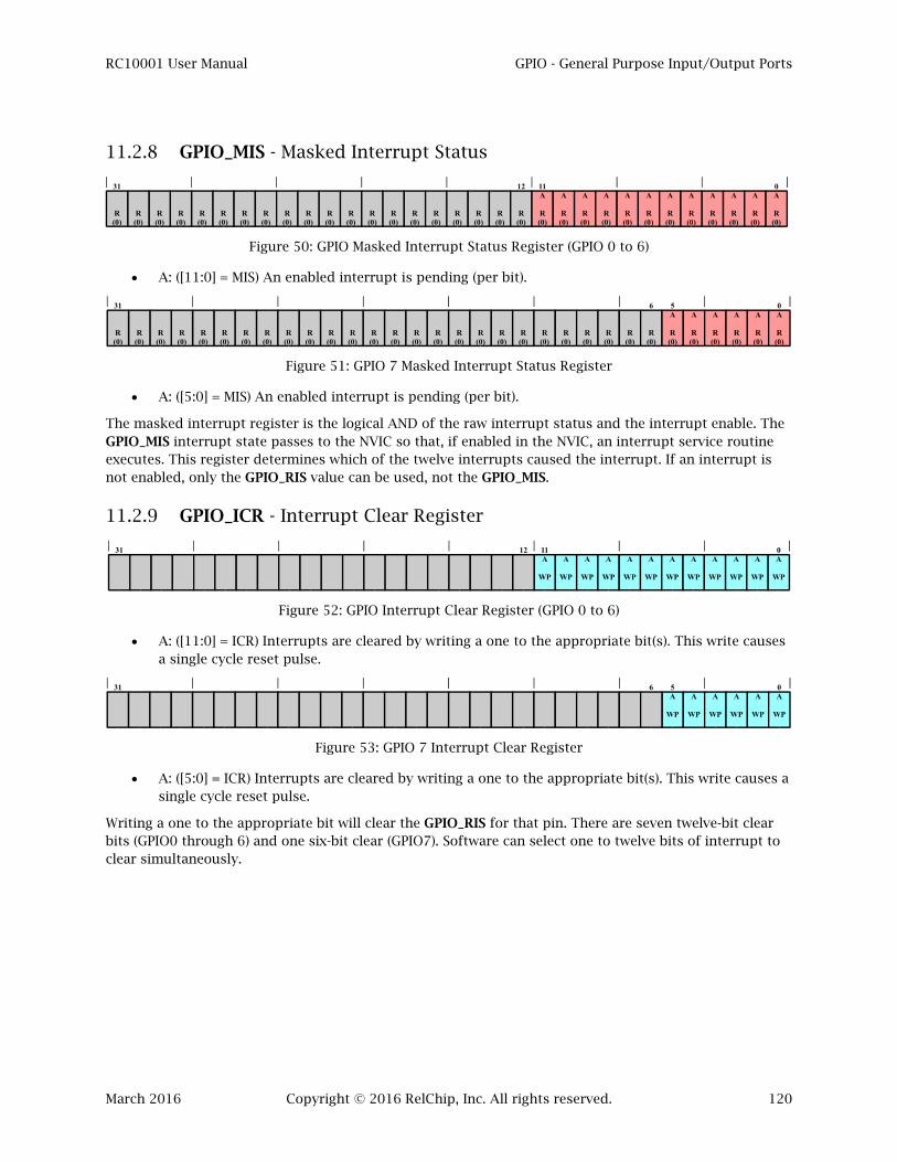
RC10001 User Manual GPIO - General Purpose Input/Output Ports
March 2016 Copyright © 2016 RelChip, Inc. All rights reserved. 120
11.2.8 GPIO_MIS - Masked Interrupt Status
Figure 50: GPIO Masked Interrupt Status Register (GPIO 0 to 6)
A: ([11:0] = MIS) An enabled interrupt is pending (per bit).
Figure 51: GPIO 7 Masked Interrupt Status Register
A: ([5:0] = MIS) An enabled interrupt is pending (per bit).
The masked interrupt register is the logical AND of the raw interrupt status and the interrupt enable. The GPIO_MIS interrupt state passes to the NVIC so that, if enabled in the NVIC, an interrupt service routine executes. This register determines which of the twelve interrupts caused the interrupt. If an interrupt is not enabled, only the GPIO_RIS value can be used, not the GPIO_MIS.
11.2.9 GPIO_ICR - Interrupt Clear Register
Figure 52: GPIO Interrupt Clear Register (GPIO 0 to 6)
A: ([11:0] = ICR) Interrupts are cleared by writing a one to the appropriate bit(s). This write causes a single cycle reset pulse.
Figure 53: GPIO 7 Interrupt Clear Register
A: ([5:0] = ICR) Interrupts are cleared by writing a one to the appropriate bit(s). This write causes a single cycle reset pulse.
Writing a one to the appropriate bit will clear the GPIO_RIS for that pin. There are seven twelve-bit clear bits (GPIO0 through 6) and one six-bit clear (GPIO7). Software can select one to twelve bits of interrupt to clear simultaneously.
R(0)
R(0)
R(0)
R(0)
R(0)
31
R(0)
R(0)
R(0)
R(0)
R(0)
R(0)
R(0)
R(0)
R(0)
R(0)
R(0)
R(0)
R(0)
R(0)
12
R(0)
11A
R(0)
A
R(0)
A
R(0)
A
R(0)
A
R(0)
A
R(0)
A
R(0)
A
R(0)
A
R(0)
A
R(0)
A
R(0)
0A
R(0)
R(0)
R(0)
R(0)
R(0)
R(0)
31
R(0)
R(0)
R(0)
R(0)
R(0)
R(0)
R(0)
R(0)
R(0)
R(0)
R(0)
R(0)
R(0)
R(0)
R(0)
R(0)
R(0)
R(0)
R(0)
R(0)
6
R(0)
5A
R(0)
A
R(0)
A
R(0)
A
R(0)
A
R(0)
0A
R(0)
31 11A
WP
A
WP
A
WP
A
WP
A
WP
A
WP
A
WP
A
WP
A
WP
A
WP
A
WP
0A
WP
12
31 5A
WP
A
WP
A
WP
A
WP
A
WP
0A
WP
6

RC10001 User Manual RAMCFG - RAM Configuration
March 2016 Copyright © 2016 RelChip, Inc. All rights reserved. 121
12 RAMCFG - RAM CONFIGURATION
The internal RAM is a 1K x 36 bit memory. Each byte of memory has a parity bit. When a write occurs, the parity is calculated and stored with the data. Read includes a parity check. RAM configuration registers handle the parity.
Testing the parity circuits occurs with the test mode register.
12.1 REGISTERS
Table 31: RAM Configuration Register Map
Register Address(1) Description
IE 0x4002_0000 Interrupt Enable
RIS 0x4002_0004 Raw Interrupt Status
MIS 0x4002_0008 Masked Interrupt Status
ICR 0x4002_0008 Interrupt Clear
TM 0x4002_000C Test Mode
- 0x4002_0010 to 0x4002_3FFF Reserved
12.1.1 RAMCFG_IE - Interrupt Enable Register
Figure 54: RAM Interrupt Enable Register
A: ([0] = IE) Interrupt Enable.
A one in the IE field enables RAM interrupts.
0A
RW(0)
R(0)
R(0)
R(0)
R(0)
R(0)
R(0)
R(0)
R(0)
R(0)
R(0)
R(0)
R(0)
R(0)
R(0)
R(0)
R(0)
R(0)
R(0)
R(0)
R(0)
31
R(0)
R(0)
R(0)
R(0)
R(0)
R(0)
R(0)
R(0)
R(0)
R(0)
1
R(0)

RC10001 User Manual RAMCFG - RAM Configuration
March 2016 Copyright © 2016 RelChip, Inc. All rights reserved. 122
12.1.2 RAMCFG_RIS - Raw Interrupt Status Register
Figure 55: RAM Raw Interrupt Status Register
A: ([0] = RIS) Raw Interrupt Status.
The read-only raw status reports parity errors independent of the interrupt enable. Parity state is polled.
12.1.3 RAMCFG_MIS - Masked Interrupt Status Register
Figure 56: RAM Masked Interrupt Status Register
A: ([0] = MIS) Masked Interrupt Status.
The read-only masked status value is the logical AND of the raw interrupt status and the interrupt enable. This is the value sent to the NVIC to service enabled interrupts.
12.1.4 RAMCFG_ICR - Interrupt Clear Register
Figure 57: RAM Interrupt Clear Register
A: ([0] = ICR) Interrupt Clear Bit.
A write of one to the ICR bit clears the interrupt. This is a write-only register sharing the RAMCFG_MIS address.
R(0)
R(0)
R(0)
R(0)
R(0)
R(0)
R(0)
R(0)
R(0)
R(0)
R(0)
R(0)
0A
R(0)
R(0)
R(0)
R(0)
R(0)
R(0)
R(0)
R(0)
R(0)
31
R(0)
R(0)
R(0)
R(0)
R(0)
R(0)
R(0)
R(0)
R(0)
R(0)
1
R(0)
R(0)
R(0)
R(0)
R(0)
R(0)
R(0)
R(0)
R(0)
R(0)
R(0)
R(0)
R(0)
0A
R(0)
R(0)
R(0)
R(0)
R(0)
R(0)
R(0)
R(0)
R(0)
31
R(0)
R(0)
R(0)
R(0)
R(0)
R(0)
R(0)
R(0)
R(0)
R(0)
1
R(0)
31 0A
WP
1

RC10001 User Manual RAMCFG - RAM Configuration
March 2016 Copyright © 2016 RelChip, Inc. All rights reserved. 123
12.1.5 RAMCFG_TM – Test Mode Register
Figure 58: RAM Test Mode Register
A: ([0] = PTM) Test Mode Enable
Writing the PTM bit causes subsequent writes to memory to write intentionally false parity for all bytes written. This process continues until clearing the PTM bit. Test code can be written to check each parity bit (byte reads from the bad locations), or a gross check of all bits. STRB and STRH write selected parity errors.
0A
RW(0)
R(0)
R(0)
R(0)
R(0)
R(0)
R(0)
R(0)
R(0)
R(0)
R(0)
R(0)
R(0)
R(0)
R(0)
R(0)
R(0)
R(0)
R(0)
R(0)
R(0)
31
R(0)
R(0)
R(0)
R(0)
R(0)
R(0)
R(0)
R(0)
R(0)
R(0)
1
R(0)

RC10001 User Manual EBCFG - External Bus Configuration
March 2016 Copyright © 2016 RelChip, Inc. All rights reserved. 124
13 EBCFG - EXTERNAL BUS CONFIGURATION
The external bus controller connects the processor to external memory and input/output devices via a “flash-nor” type bus. The bus is a derivation of standard multiplexed busses used in other systems. As such, it is compatible with many components.
The bus is a thirty-two bit address/data multiplexed bus (standard configuration), although an eight bit option is available). An additional four parity lines are added (per byte basis). This bus supports configuration read/writes through a configuration register enable pin (CRE), and slow devices with a EWAIT handshake signal.
All pins of the external bus can be tri-stated, allowing for multi-master busses. Use of a GPIO pin to connect interrupts (wire-or) for multi-master systems is possible.
Nomenclature Note: EBCFG is the external bus configuration. EXBUS is the external bus itself.
13.1 PIN DESCRIPTION
Table 32 defines the external bus pin names and functions.
Table 32: External Bus Signals
Pin Type Description
ECLK Out Bus Clock
ECSAn ECSBn ECSCn ECSDn
Out Chip Selects
EADVn Out Address Valid
EOEn Out Output Enable (External Enabled)
EWEn Out Write Enable
EBW[3:0]n Out Byte Write Enable
EADQ[31:0] In/Out Address/Data Bus
EPDQ[3:0] In/Out Parity
ECRE Out Configuration Register Enable
EWAIT In Wait
EINT In Interrupt
RC10001 User Manual EBCFG - External Bus Configuration
March 2016 Copyright © 2016 RelChip, Inc. All rights reserved. 125
13.2 OPERATION
The external bus of the RC10001 operates in two or more cycles. The primary cycles are address and data. Slow peripherals insert one or more wait cycles. When configured for the thirty-two bit bus, a single address cycle followed by a single data cycle is the minimum required for a transfer. In the eight bit configuration, a single address cycle is followed by a burst of four bytes is required.
In the thirty-two bit mode, writing generates thirty-two bits mapped to the location. For word write, the thirty-two bits map directly, and all four byte write signals (BW#n) activate. For a halfword write, the sixteen bits appear on both the lower and upper halfwords of the bus. Byte writes control the halfword to write. For a byte write, the bytes appears in each of the four bytes of the thirty-two bit bus. One byte write is selected to write the appropriate byte.
During a thirty-two bit read, the RC10001 maps the appropriate bit field to the internal bus.
ECLK strobes during active cycles unless the CEH bit of EBCFG_CONFIG is set. Setting CEH adds one clock cycle with the CS signals de-asserted. If external cycles occur often enough (example is fetching instructions), ECLK appears to be constantly running.
13.2.1 Thirty-two Bit Read Operations
The standard method to fetch instructions or read data from external memory is a thirty-two bit read as shown in Figure 59. An address cycle begins with the microcontroller issuing EADVn low, ECS[A-D]n low, and the address on EADQ[31:0]. A data cycle will then begin with EWAIT issued by the responding external device. Figure 60 shows one cycle of latency inserted by the peripheral to allow response time.
The address cycle serves to clock in the address on the rising edge of the clock at the external device. EADVn and ECS[A-D]n are used to select the device and signal the address cycle.
The external device controls the response via the EWAIT signal. When held low, the microcontroller will keep issuing external bus clocks waiting for valid data (see Figure 60). EWAIT issues concurrent with valid data. There can be alterations to the EWAIT response via the external bus configuration, EBCFG_BUS_CONFIG.
Once EWAIT is high, a data cycle begins. On the clock edge, the data is loaded into the RC10001. The data is mapped onto the internal thirty-two bit bus. Unused bits (halfword and byte) are set low.

RC10001 User Manual EBCFG - External Bus Configuration
March 2016 Copyright © 2016 RelChip, Inc. All rights reserved. 126
Figure 59: Thirty-Two Bit External Read
Figure 60: Thirty-two Bit External Read with a Cycle of Latency
ECLK
EADVn
ECS#n
EOEn
EADQ[31:0]
EPDQ[3:0]
EWAIT
Parity
DataAddress
ECLK
EADVn
ECS#n
EOEn
EADQ[31:0]
EPDQ[3:0]
EWAIT
Parity
DataAddress

RC10001 User Manual EBCFG - External Bus Configuration
March 2016 Copyright © 2016 RelChip, Inc. All rights reserved. 127
13.2.2 Thirty-two Bit Write Operations
The standard method to write data to external memory is a thirty-two bit data write as shown in Figure 61. An address cycle begins with the microcontroller issuing EADVn low, ECS[A-D]n low, EWEn low, and the address on EADQ[31:0]. Data appears on the cycle following the address, and the byte writes assert. The data write cycle terminates when EWAIT asserts. Slower peripherals require wait cycle(s) (Figure 62).
The address cycle serves to clock in the address on the rising edge of the clock at the external device. EADVn and ECS[A-D]n are used to select the device and signal the address cycle. EWEn signals a write operation.
The external device controls the response via the EWAIT signal. When held low, the microcontroller will keep issuing external bus clocks and data waiting for EWAIT. Raising EWAIT signals write completion. There can be alterations to this response via the external bus configuration, EBCFG_BUS_CONFIG.
Once EWAIT is high, the data cycle finishes. The data appearing on the bus from the first cycle to the last is the data to write. If a halfword is being written, the halfword appears in both the low thirty-two bits and the high thirty-two bits, but the appropriate byte write signals (EBW[0-3]n) are asserted. A similar operation occurs with a byte write except all four bytes contain the data to write, and only one of EBW[0-3]n is asserted.
Figure 61: Thirty-Two Bit External Write
ECLK
EADVn
ECS#n
EBW#n
EADQ[31:0]
EPDQ[3:0]
EWAIT
Parity
DataAddress
EWEn
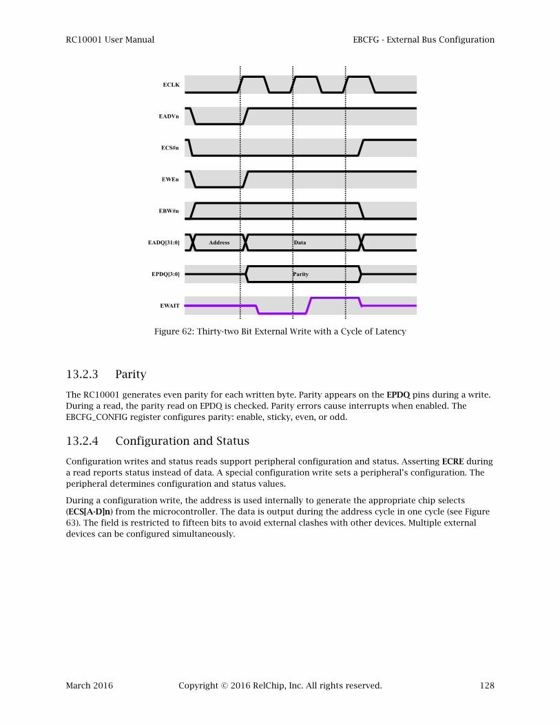
RC10001 User Manual EBCFG - External Bus Configuration
March 2016 Copyright © 2016 RelChip, Inc. All rights reserved. 128
Figure 62: Thirty-two Bit External Write with a Cycle of Latency
13.2.3 Parity
The RC10001 generates even parity for each written byte. Parity appears on the EPDQ pins during a write. During a read, the parity read on EPDQ is checked. Parity errors cause interrupts when enabled. The EBCFG_CONFIG register configures parity: enable, sticky, even, or odd.
13.2.4 Configuration and Status
Configuration writes and status reads support peripheral configuration and status. Asserting ECRE during a read reports status instead of data. A special configuration write sets a peripheral’s configuration. The peripheral determines configuration and status values.
During a configuration write, the address is used internally to generate the appropriate chip selects (ECS[A-D]n) from the microcontroller. The data is output during the address cycle in one cycle (see Figure 63). The field is restricted to fifteen bits to avoid external clashes with other devices. Multiple external devices can be configured simultaneously.
ECLK
EADVn
ECS#n
EBW#n
EADQ[31:0]
EPDQ[3:0]
EWAIT
Parity
DataAddress
EWEn

RC10001 User Manual EBCFG - External Bus Configuration
March 2016 Copyright © 2016 RelChip, Inc. All rights reserved. 129
Figure 63: External Configuration Write
13.2.5 WAIT Options
The EWAIT pin is wire-or connected to all the external devices. Each external device can drive EWAIT low to delay the data cycle completion. When ready, this device should then drive EWAIT high. An external pull up keeps EWAIT high.
The microcontroller can operate with a fixed latency, indefinite wait, or limited wait. EBCFG_BUS_CONFIG register configures the latency. Fixed latency ignores the EWAIT pin, setting the number of delayed data cycles to a value (0 to 7). Indefinite wait will suspend further progress until EWAIT assertion. Limited wait is identical to indefinite, except that after thirty-two cycles, the operation aborts and a bus error occurs.
13.2.6 External Bus Interrupts
A wire-or EINT pin inputs external interrupts. Driving EINT high causes an interrupt when enabled.
13.2.7 Eight-Bit Operations
Four sequential data cycles with eight-bit data characterize the eight-bit mode. The data bytes are sequenced little endian with BW0n controlling the writes. Note that status reads are output as a sequence of bytes, but the configuration write is a single cycle operation.
ECLK
EADVn
ECS#n
EADQ[13:0] Data
EWEn
AddressEADQ[14]
ECRE
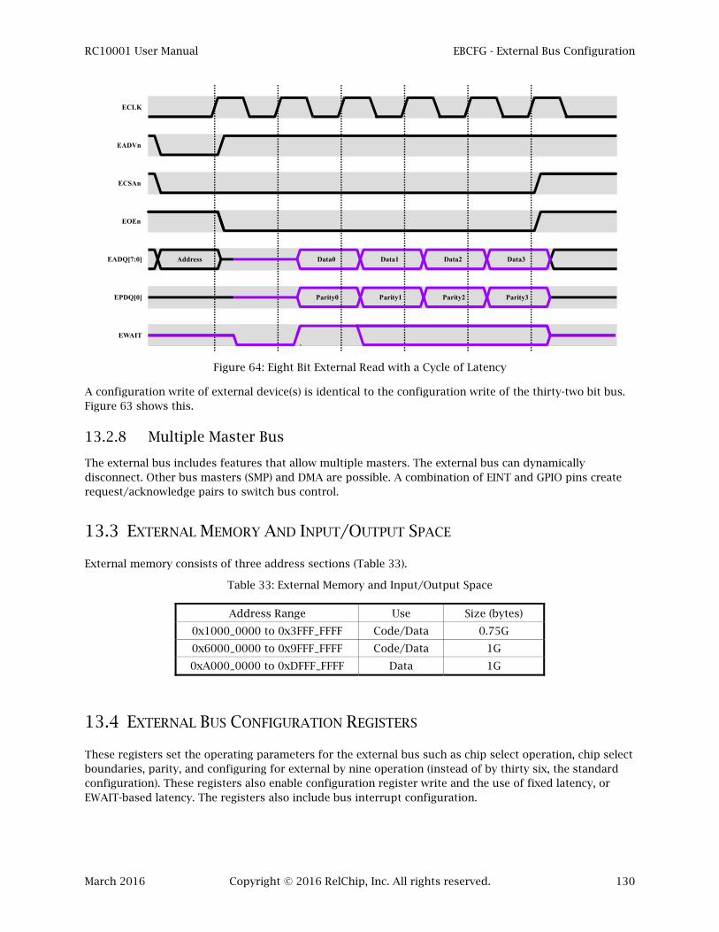
RC10001 User Manual EBCFG - External Bus Configuration
March 2016 Copyright © 2016 RelChip, Inc. All rights reserved. 130
Figure 64: Eight Bit External Read with a Cycle of Latency
A configuration write of external device(s) is identical to the configuration write of the thirty-two bit bus. Figure 63 shows this.
13.2.8 Multiple Master Bus
The external bus includes features that allow multiple masters. The external bus can dynamically disconnect. Other bus masters (SMP) and DMA are possible. A combination of EINT and GPIO pins create request/acknowledge pairs to switch bus control.
13.3 EXTERNAL MEMORY AND INPUT/OUTPUT SPACE
External memory consists of three address sections (Table 33).
Table 33: External Memory and Input/Output Space
Address Range Use Size (bytes)
0x1000_0000 to 0x3FFF_FFFF Code/Data 0.75G
0x6000_0000 to 0x9FFF_FFFF Code/Data 1G
0xA000_0000 to 0xDFFF_FFFF Data 1G
13.4 EXTERNAL BUS CONFIGURATION REGISTERS
These registers set the operating parameters for the external bus such as chip select operation, chip select boundaries, parity, and configuring for external by nine operation (instead of by thirty six, the standard configuration). These registers also enable configuration register write and the use of fixed latency, or EWAIT-based latency. The registers also include bus interrupt configuration.
ECLK
EADVn
ECSAn
EOEn
EADQ[7:0]
EPDQ[0]
EWAIT
Parity0
Data0Address Data1 Data2 Data3
Parity1 Parity2 Parity3

RC10001 User Manual EBCFG - External Bus Configuration
March 2016 Copyright © 2016 RelChip, Inc. All rights reserved. 131
Table 34: External Bus Configuration Register Map
Register Address Description
CONFIG 0x4002_8000 Configuration
BUS_CONFIG 0x4002_8004 Bus Configuration
IE 0x4002_8008 Interrupt Enable
RIS 0x4002_800C Raw Interrupt Status
MIS 0x4002_8010 Masked Interrupt Status
ICR 0x4002_8010 Interrupt Clear
ERR_CONFIG 0x4002_8014 Error Configuration
- 0x4002_8018 to 0x4002_801C Reserved
MIN_A 0x4002_8020 Minimum EACSAN Address
MAX_A 0x4002_8024 Maximum EACSAN Address
MIN_B 0x4002_8028 Minimum EACSBN Address
MAX_B 0x4002_802C Maximum EACSBN Address
MIN_C 0x4002_8030 Minimum EACSCN Address
MAX_C 0x4002_8034 Maximum EACSCN Address
MIN_D 0x4002_8038 Minimum EACSDN Address
MAX_D 0x4002_803C Maximum EACSDN Address
- 0x4002_8040 to 0x4002_BFFF Reserved
13.4.1 EBCFG_CONFIG - Configuration Register
Figure 65: EXBUS Configuration Register
A: ([0] = CSA) Enable ECSAn to go low when the minimum and maximum addresses are satisfied, B: ([1] = CSB) Enable ECSBn to go low when the minimum and maximum addresses are satisfied, C: ([2] = CSC) Enable ECSCn to go low when the minimum and maximum addresses are satisfied, D: ([3] = CSD) Enable ECSDn to go low when the minimum and maximum addresses are satisfied, E: ([4] = PEVEN) When set (and the PSTICK bit is low) parity is even. If the PSTICK bit is high, parity
is always low. When not set and the PSTICK bit is low, parity is odd. If the PSTICK bit is high, parity is always high,
F: ([5] = PSTICK) Sticky parity changes the sense of the PEVEN bit. This bit high sets fixed logic levels for external bus parity. A low bit dictates even or odd parity (determined by PEVEN),
G: ([6] = X9) When set to one, the external bus is nine bits wide (eight data and one parity). Otherwise, it is thirty six bits wide (thirty-two data and four parity bits),
H: ([7] = CEH) When set to one, one cycle of no chip select (ECSAn, ECSBn, ECSCn, and ECSDn all one) is inserted between external accesses.
1B
RW(0)
R(0)
3D
RW(0)
4E
RW(0)
5F
RW(0)
6G
RW(0)
7H
RW(0)
R(0)
R(0)
R(0)
R(0)
31
R(0)
R(0)
0A
RW(0)
2C
RW(0)
R(0)
R(0)
R(0)
R(0)
R(0)
R(0)
R(0)
R(0)
R(0)
R(0)
R(0)
R(0)
8
R(0)
R(0)
R(0)
R(0)
R(0)

RC10001 User Manual EBCFG - External Bus Configuration
March 2016 Copyright © 2016 RelChip, Inc. All rights reserved. 132
13.4.2 EBCFG_BUS_CONFIG - Bus Configuration Register
Figure 66: EXBUS Bus Configuration Register
A: ([0] = CRE) Configuration Register Enable. B: ([3:1] = LAT) Latency Cycles. This field defines the number of extra data cycles used to meet
latency. Valid values are 0 through 7. C: ([4] = FIXED) Enable Fixed Latency Mode. If this bit is zero, the RC10001 waits for the EWAIT
signal to end the data cycles. If it is one, the fixed delay in the LAT field is used.
Bus latency can be fixed (FIXED bit) to the value in the latency (LAT) field. If FIXED is cleared (zero), the RC10001 waits for the EWAIT pin to go high to finish the operation. This may be multiple cycles, and may cause a bus error (see EBCFG_ERR_CONFIG - Error Configuration Register). If FIXED is set, the fixed latency found in LAT is used. The latency is the number of delay cycles between the address and data cycles of the bus.
The CRE field is output on the CRE pin. The CRE, or configuration register enable, signals external components that a write is a configuration write, and a read is a status read.
1B
RW(0)
R(0)
3B
RW(0)
4C
RW(0)
R(0)
R(0)
R(0)
R(0)
31
R(0)
R(0)
0A
RW(0)
B
RW(0)
R(0)
R(0)
R(0)
R(0)
R(0)
R(0)
R(0)
R(0)
R(0)
R(0)
R(0)
R(0)
5
R(0)
R(0)
R(0)
R(0)
R(0)
R(0)
R(0)
R(0)

RC10001 User Manual EBCFG - External Bus Configuration
March 2016 Copyright © 2016 RelChip, Inc. All rights reserved. 133
13.4.3 EBCFG_IE - Interrupt Enable Register
Figure 67: EXBUS Interrupt Enable Register
A: ([0] = PAR) Enable the Parity Interrupt for the External Bus. B: ([1] = EINT) Enable the External Bus Interrupt.
This register enables the two possible interrupts for the external bus. The EXBUS NVIC interrupt services these interrupts.
13.4.4 EBCFG_RIS - Raw Interrupt Status Register
Figure 68: EXBUS Raw Interrupt Status Register
A: ([0] = PAR) External Bus Parity Error Interrupt Precursor State, B: ([1] = EINT) External Bus Interrupt Precursor State.
This register reports the interrupt status independent of the interrupt enable.
13.4.5 EBCFG_MIS - Masked Interrupt Status Register
Figure 69: EXBUS Masked Interrupt Status Register
A: ([0] = PAR) External Bus Parity Error Interrupt State, B: ([1] = EINT) External Bus Interrupt State.
The MIS register contains the value of the raw interrupt after masked by the enable. This is the NVIC input.
1B
RW(0)
R(0)
R(0)
R(0)
R(0)
R(0)
31
R(0)
R(0)
0A
RW(0)
R(0)
R(0)
R(0)
R(0)
R(0)
R(0)
R(0)
R(0)
R(0)
R(0)
R(0)
R(0)
2
R(0)
R(0)
R(0)
R(0)
R(0)
R(0)
R(0)
R(0)
R(0)
R(0)
R(0)
R(0)
R(0)
R(0)
R(0)
R(0)
R(0)
R(0)
R(0)
R(0)
R(0)
R(0)
R(0)
0A
R(0)
R(0)
R(0)
R(0)
R(0)
R(0)
R(0)
R(0)
R(0)
31
R(0)
R(0)
R(0)
R(0)
R(0)
R(0)
R(0)
R(0)
R(0)
2
R(0)
1B
R(0)
R(0)
R(0)
R(0)
R(0)
R(0)
R(0)
R(0)
R(0)
R(0)
R(0)
R(0)
R(0)
0A
R(0)
R(0)
R(0)
R(0)
R(0)
R(0)
R(0)
R(0)
R(0)
31
R(0)
R(0)
R(0)
R(0)
R(0)
R(0)
R(0)
R(0)
R(0)
2
R(0)
1B
R(0)
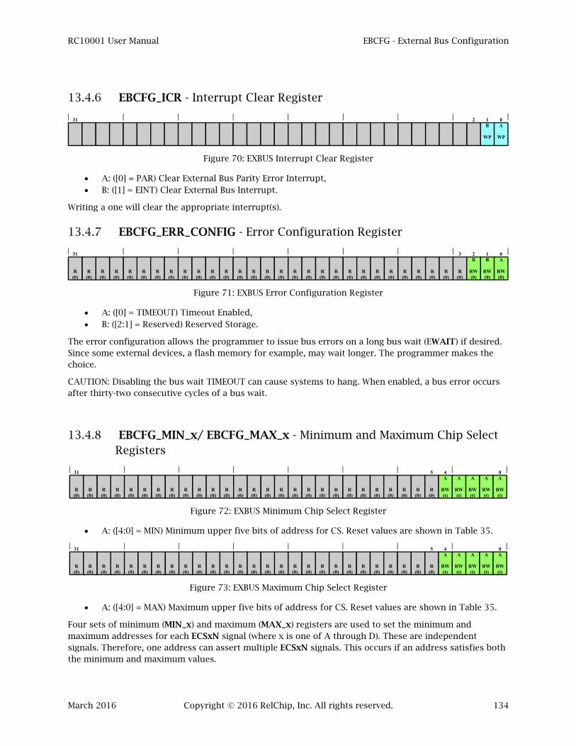
RC10001 User Manual EBCFG - External Bus Configuration
March 2016 Copyright © 2016 RelChip, Inc. All rights reserved. 134
13.4.6 EBCFG_ICR - Interrupt Clear Register
Figure 70: EXBUS Interrupt Clear Register
A: ([0] = PAR) Clear External Bus Parity Error Interrupt, B: ([1] = EINT) Clear External Bus Interrupt.
Writing a one will clear the appropriate interrupt(s).
13.4.7 EBCFG_ERR_CONFIG - Error Configuration Register
Figure 71: EXBUS Error Configuration Register
A: ([0] = TIMEOUT) Timeout Enabled, B: ([2:1] = Reserved) Reserved Storage.
The error configuration allows the programmer to issue bus errors on a long bus wait (EWAIT) if desired. Since some external devices, a flash memory for example, may wait longer. The programmer makes the choice.
CAUTION: Disabling the bus wait TIMEOUT can cause systems to hang. When enabled, a bus error occurs after thirty-two consecutive cycles of a bus wait.
13.4.8 EBCFG_MIN_x/ EBCFG_MAX_x - Minimum and Maximum Chip Select Registers
Figure 72: EXBUS Minimum Chip Select Register
A: ([4:0] = MIN) Minimum upper five bits of address for CS. Reset values are shown in Table 35.
Figure 73: EXBUS Maximum Chip Select Register
A: ([4:0] = MAX) Maximum upper five bits of address for CS. Reset values are shown in Table 35.
Four sets of minimum (MIN_x) and maximum (MAX_x) registers are used to set the minimum and maximum addresses for each ECSxN signal (where x is one of A through D). These are independent signals. Therefore, one address can assert multiple ECSxN signals. This occurs if an address satisfies both the minimum and maximum values.
31 1B
WP
0A
WP
2
1B
RW(0)
R(0)
R(0)
R(0)
R(0)
R(0)
31
R(0)
R(0)
0A
RW(0)
R(0)
R(0)
R(0)
R(0)
R(0)
R(0)
R(0)
R(0)
R(0)
R(0)
R(0)
R(0)
3
R(0)
R(0)
R(0)
R(0)
R(0)
R(0)
R(0)
R(0)
R(0)
R(0)
2B
RW(0)
A
RW(t)
R(0)
R(0)
R(0)
R(0)
R(0)
31
R(0)
R(0)
0A
RW(t)
R(0)
R(0)
R(0)
R(0)
R(0)
R(0)
R(0)
R(0)
R(0)
R(0)
R(0)
R(0)
5
R(0)
R(0)
R(0)
R(0)
R(0)
R(0)
R(0)
R(0)
A
RW(t)
A
RW(t)
4A
RW(t)
A
RW(t)
R(0)
R(0)
R(0)
R(0)
R(0)
31
R(0)
R(0)
0A
RW(t)
R(0)
R(0)
R(0)
R(0)
R(0)
R(0)
R(0)
R(0)
R(0)
R(0)
R(0)
R(0)
5
R(0)
R(0)
R(0)
R(0)
R(0)
R(0)
R(0)
R(0)
A
RW(t)
A
RW(t)
4A
RW(t)

RC10001 User Manual EBCFG - External Bus Configuration
March 2016 Copyright © 2016 RelChip, Inc. All rights reserved. 135
The register contains five bits ([4:0]). These map to the most significant bits in the RC10001 address space (A[31:27]). The entries are inclusive. If for example,
MIN = 0x5, and MAX = 0x5, then the range is 0x2800_0000 to 0x2FFF_FFFF MIN = 0x6, and MAX = 0x10, then the range is 0x3000_0000 to 0x87FFF_FFFF
Table 35: Reset Values for CS Address Range
CS Pin Minimum Maximum
ECSAn 0x0C 0x0F
ECSBn 0x10 0x13
ECSCn 0x14 0x17
ECSDn 0x18 0x1F
RC10001 User Manual UART - Universal Asynchronous Receiver/Transmitter
March 2016 Copyright © 2016 RelChip, Inc. All rights reserved. 136
14 UART - UNIVERSAL ASYNCHRONOUS RECEIVER/TRANSMITTER
The UART implements standard RS-232, standard RS-485, and partially the LIN 2.0 standard interfaces. The UART includes separate transmit and receive FIFOs to avoid loading the processor. The UART serial interfaces can operate at frequencies up to one eighth of the processor clock speed.
14.1 FEATURES
Configurable BAUD Rate variable, up to One Eighth Processor Clock Frequency Data Width: 5, 6, 7, or 8 Bits Parity: Even, Odd, Sticky, or None Stop Bits: 1 or 1.5 Interrupts Transmit FIFO, 16 bytes deep Receive FIFO, 16 bytes deep Programmable FIFO Trigger Levels: 1, 4, 8, and 14 bytes Receive Timeout Modem Status Error Codes Modem Control: CTSN, DCDN, DSRN, RTSN, DTRN, and RIN False Start Bit Detection Programmable Hardware Flow Control (RS-485) Line Break Generation and Detection (LIN 2.0)
14.2 MODES OF OPERATION
The interface has three basic modes of operation: RS-232, RS-485, and LIN 2.0. The modes are not mutually exclusive. Hybrid interfaces are possible.
All modes share two sixteen byte FIFOs: one receiver FIFO and one transmitter FIFO. The independent FIFOs load the processor less, and allow staging of responses. For example, a protocol may require transmitting a response to an initial reception. The transmit FIFO can be loaded “early” if required and direction controlled.
Standard UART interrupts are included. In addition, LIN 2.0 functions add two more interrupts.
To operate the UART peripheral, the appropriate clock in SYSCON_AHBCLKCTRL - Clock Enable Register. Upon reset, this clock is disabled.

RC10001 User Manual UART - Universal Asynchronous Receiver/Transmitter
March 2016 Copyright © 2016 RelChip, Inc. All rights reserved. 137
14.2.1 RS-232
All standard pins, registers, and modes for a RS-232 interface are included. The registers are all eight bit (for the RS-232), and the register addressing is standard. One exception is the UART_LCR register. It includes a ninth bit to set the eight or sixteen cycle sample divisor, but setting this low keeps the standard sixteen cycle sample.
The UART baud rate is determined by the sample rate (DIV8 of the UART_LCR register) and the clock divisor (the UART_DLL and UART_DLM registers). The DIV8 bit allows eight clock cycles per data cycle instead of 16 clock cycles per data cycle to achieve higher baud rates. The highest possible baud rate is the system clock rate divided by eight.
14.2.2 RS-485
RS-485 mode allows the part to be an addressable slave as well as a master. The master can transmit the address flagged by a parity error. If the slave detects high parity, the address is verified by comparing the incoming data and UART_RS485ADDR register. If the parity bit is set LOW, data is implied. The UART can be programmed to automatically reject or accept data if the address is not its own.
This mode requires enabling parity.
The RS-485 physical receiver and transmitter are located outside the RC10001. The RC10001 interface provides a single receiver pin, a single transmitter pin, and a transmit enable pin.
14.2.2.1 Normal Multidrop Mode (NMM)
Setting the UART_RS485CTRL NMMEN bit enables the multidrop mode. Parity errors occur on addresses.
If the RS485CTRL NMMEN bit is on, the receiver only becomes active with an address match. With a match the address is received. The code decides if the receiver should remain enabled.
If the RS485CTRL NMMEN bit is off, the receiver is enabled and all bytes are received and placed in the RXFIFO independent of address or data meaning.
14.2.2.2 Auto Address Detection (ADD)
When the NMMEN and AADEN bits are set in the UART_RS485CTRL register, the UART is in auto address detect mode.
When the receiver is disabled (UART_RS485CTRL RXDIS set), all data and addresses are ignored. The receiver will compare the address byte (parity error) to the 8-bit UART_RS485ADDR register. If the address matches, it is pushed onto the FIFO and the receiver is automatically enabled (UART_RS485CTRL RXDIS cleared). An RX data ready interrupt will be queued.
While the receiver is enabled, all data and matching address will be added to the Receiver FIFO. This action will continue until an address request does not match. The UART_RS485CTRL RXDIS is set on an address mismatch. The non-matching address is not stored on the FIFO.

RC10001 User Manual UART - Universal Asynchronous Receiver/Transmitter
March 2016 Copyright © 2016 RelChip, Inc. All rights reserved. 138
14.2.2.3 Auto Direction Control
Automatic direction control for the interface is hardware controlled when the UART_RS485CTRL DCTRL bit is set. The hardware will use RTSN or DTRN to command direction control when the DCTRL bit is set. The SEL bit selects RSTN or DTRN direction control. The OINV bit controls direction control polarity.
Automatic delay from the end of a transmission to the de-assertion of the command direction is set with the UART_RS486DLY register.
14.2.3 LIN
The UART offers hardware support for the LIN protocol as either a master or a slave. Setting the EN bit the UART_LCTL register enables the LIN mode. An initial SYNC-BREAK begins a LIN message. This Synch Break is a transmission of a series of “0” data. The SYNC-Data Field (0x55) follows a SYNC-BREAK field. The LIN mode uses TIMER 32A resources. Thus, the TIMER 32A clock must be enabled (SYSCON_AHBCLKCTRL - Clock Enable Register) and configured.
For the LIN mode, the UART is configured as follows:
1. Configure the UART for 1 start bit, 8 data bits, no parity, and 1 stop bit; 2. Enable the Transmit FIFO; 3. Set the EN bit in the UART LCTL register; 4. Enable the clock for TIMER32A. This timer will not be available for normal use when configured
for the LIN interface.
When preparing to send a LIN message, the TXFIFO should contain the Sync data (0x55) at FIFO location 0 and the identifier data at location 1, followed by the transmit data, and with the checksum in the final FIFO entry.
For details on the LIN protocol, please see the “LIN 2.0 Specification.”
14.2.3.1 LIN Master
The creation of a message for the LIN master requires:
1. Configure as above; 2. Set the BCS bit of the UART_LCR Register (Break Control), It will automatically clear according to
the BAUD Rate; 3. Store the Sync Data (0x55) in the Transmit FIFO; 4. Store the Identifier Data in the Transmit FIFO; 5. Store (Send) Desired Data.
The LIN Master will then receive any required data from slaves, or send required data to slaves.
If the UART_LCR BCS bit is set, but the LIN mode is not active, the transmitter output is low.

RC10001 User Manual UART - Universal Asynchronous Receiver/Transmitter
March 2016 Copyright © 2016 RelChip, Inc. All rights reserved. 139
14.2.3.2 LIN Slave
The LIN slave receives a CTRL-BREAK sequence (which can cause an interrupt or be polled) to begin its response. TIMER 32A is used to auto-baud detect on the sync byte. The code will determine the baud rate from the timer, and set the UART_DLL and UART_DLM registers appropriately. After the sync sequence, the TIMER32A_CAP register holds the baud value, multiplied by 64 (or 32 for 8 cycle samples), allowing sample clocks for four bits.
The receiver FIFO saves a zero representing the CTRL-BREAK, the sync byte (0x55), and the data that follows. All other protocol issues reside in software. A frame will always contain a BREAK, a SYNC, and a Protected ID.
Received data is stored in the FIFO, and interrupts indicate data presence.
14.2.4 Test Modes
Loopback test mode is set by a bit in the UART_MCR register. This mode connects transmitter and output signals to receiver and input signals for tests driven by internal code.
14.3 PIN DESCRIPTION
Table 36 describes the pins in various modes.
Table 36: UART Pinout
Pin RS-232 RS-485 LIN 2.0 Type Description
RXD_GPIO2_3 RxD RX1 TX/RX2 In Receive Data
TXD_GPIO2_4 TxD TX1 RX/RX2 Out Transmit Data
CTSN_GPIO2_5 CTSN - - In Clear to Send
DSRN_GPIO2_6 DSRN - - In Data Set Ready
RIN_GPIO2_7 RIN - - In Ring Indicator
DCDN_GPIO2_8 DCDN - - In Data Carrier Detect
RTSN_GPIO2_9 RTSN DIR1 - Out Request to Send
DTRN_GPIO2_10 DTRN - - Out Data Terminal Ready
OUT1_GPIO2_11 OUT1 - - Out General Purpose
OUT2_GPIO3_0 OUT2 - - Out General Purpose
Notes:
1. The transmitter, receiver, and direction functions require an external physical interface circuit. 2. The transmitter and receiver lines are common on the LIN bus. The electrical specs for the
physical interface require an external circuit.

RC10001 User Manual UART - Universal Asynchronous Receiver/Transmitter
March 2016 Copyright © 2016 RelChip, Inc. All rights reserved. 140
14.4 REGISTERS
The first twelve registers are the standard RS-232 register interface (byte-wide registers). These byte-wide registers should still be read-written as full word registers. The RS-485 interface uses these registers and three specific control registers. One additional register is required to control the LIN interface.
Table 37: UART Registers
Register DLAB Address(1) Description
DLL 1 0x4000_8000 Divisor Latch LSB
THR 0 0x4000_8000 Transmit Holding
RBR 0 0x4000_8000 Receiver Buffer
DLM 1 0x4000_8004 Divisor Latch MSB
IE 0 0x4000_8004 Interrupt Enable
FCR X 0x4000_8008 FIFO Control
IIR X 0x4000_8008 Interrupt Identification
LCR X 0x4000_800C Line Control
MCR X 0x4000_8010 Modem Control
LSR X 0x4000_8014 Line Status
MSR X 0x4000_8018 Modem Status
SCR X 0x4000_801C Scratch
- X 0x4000_8020 to 0x4000_802F Reserved
TER X 0x4000_8030 Transmit Enable
- X 0x4000_8034 to 0x4000_804B Reserved
RS485CTRL X 0x4000_804C RS485 Control
RS485ADDR X 0x4000_8050 RS485 Address Match
RS485DLY X 0x4000_8054 RS485 Turnaround Delay
- X 0x4000_8058 to 0x4000_805F Reserved
LCTL X 0x4000_8060 LIN Control
- X 0x4000_8064 to 0x4000_806F Reserved
- X 0x4000_8070 to 0x4000_bFFF Reserved

RC10001 User Manual UART - Universal Asynchronous Receiver/Transmitter
March 2016 Copyright © 2016 RelChip, Inc. All rights reserved. 141
14.4.1 UART_DLL – LSB Divisor Latch Register
Figure 74: UART LSB Divisor Latch Register
A: ([7:0] = DLL) Low order byte of the divisor.
The UART_DLM (divisor [15:8]) and UART_DLL (divisor[7:8]) registers form a sixteen bit divisor for the clock. This divisor determines the BAUD rate for the UART. It is accessed by setting the DLAB bit. The BAUD rate is:
∗ 8
Where,
BAUD = the BAUD Rate (Frequency)
SFREQ = the System Clock Frequency
DIV = the Divisor Obtained from {UART_DLM, UART_DLL}
DIV8 = the DIV8 Bit in the UART_LCR Register. A 0 Bit Defines DIV8 = 16, a 1 Bit Defines DIV8 = 8
14.4.2 UART_DLM – MSB Divisor Latch Register
Figure 75: UART MSB Divisor Latch Register
A: ([7:0] = DLM) High order byte of the divisor.
The UART_DLM register is the most significant 8 bits of the baud rate divisor. It is accessed by setting the DLAB bit.
14.4.3 UART_THR – Transmit Holding Register
Figure 76: UART Transmit Holding Register
A: ([7:0] = THR) Transmit data FIFO insertion point.
The UART_THR is the head of the transmit FIFO. Data transmits from this FIFO. If no current transmission, the data written will initiate transmission. If the FIFO is full, an enabled interrupt will assert.
This is a write-only register sharing the address of the UART_RBR receive buffer. DLAB must be low to access this register.
A
RW(0)
R(0)
R(0)
R(0)
R(0)
R(0)
31
R(0)
R(0)
0A
RW(1)
R(0)
R(0)
R(0)
R(0)
R(0)
R(0)
R(0)
R(0)
R(0)
R(0)
R(0)
R(0)
8
R(0)
R(0)
R(0)
R(0)
R(0)
7A
RW(0)
A
RW(0)
A
RW(0)
A
RW(0)
A
RW(0)
A
RW(0)
A
RW(0)
R(0)
R(0)
R(0)
R(0)
R(0)
31
R(0)
R(0)
0A
RW(0)
R(0)
R(0)
R(0)
R(0)
R(0)
R(0)
R(0)
R(0)
R(0)
R(0)
R(0)
R(0)
8
R(0)
R(0)
R(0)
R(0)
R(0)
7A
RW(0)
A
RW(0)
A
RW(0)
A
RW(0)
A
RW(0)
A
RW(0)
31A
W
0A
W
8A
W
A
W
A
W
A
W
A
W
7A
W
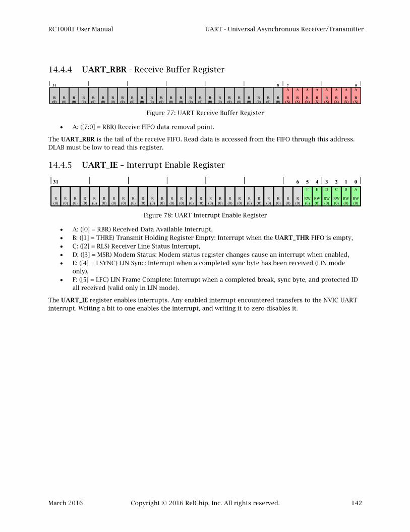
RC10001 User Manual UART - Universal Asynchronous Receiver/Transmitter
March 2016 Copyright © 2016 RelChip, Inc. All rights reserved. 142
14.4.4 UART_RBR - Receive Buffer Register
Figure 77: UART Receive Buffer Register
A: ([7:0] = RBR) Receive FIFO data removal point.
The UART_RBR is the tail of the receive FIFO. Read data is accessed from the FIFO through this address. DLAB must be low to read this register.
14.4.5 UART_IE – Interrupt Enable Register
Figure 78: UART Interrupt Enable Register
A: ([0] = RBR) Received Data Available Interrupt, B: ([1] = THRE) Transmit Holding Register Empty: Interrupt when the UART_THR FIFO is empty, C: ([2] = RLS) Receiver Line Status Interrupt, D: ([3] = MSR) Modem Status: Modem status register changes cause an interrupt when enabled, E: ([4] = LSYNC) LIN Sync: Interrupt when a completed sync byte has been received (LIN mode
only), F: ([5] = LFC) LIN Frame Complete: Interrupt when a completed break, sync byte, and protected ID
all received (valid only in LIN mode).
The UART_IE register enables interrupts. Any enabled interrupt encountered transfers to the NVIC UART interrupt. Writing a bit to one enables the interrupt, and writing it to zero disables it.
R(0)
R(0)
R(0)
R(0)
R(0)
R(0)
R(0)
R(0)
R(0)
R(0)
R(0)
R(0)
0A
R(X)
R(0)
R(0)
R(0)
R(0)
R(0)
R(0)
R(0)
R(0)
31
R(0)
R(0)
R(0)
8
R(0)
A
R(X)
A
R(X)
A
R(X)
A
R(X)
A
R(X)
A
R(X)
7A
R(X)
31 056E
RW(0)
D
RW(0)
B
RW(0)
R(0)
R(0)
R(0)
R(0)
R(0)
R(0)
R(0)
R(0)
R(0)
R(0)
4 3 2 1F
RW(0)
C
RW(0)
A
RW(0)
R(0)
R(0)
R(0)
R(0)
R(0)
R(0)
R(0)
R(0)
R(0)
R(0)
R(0)
R(0)
R(0)
R(0)
R(0)
R(0)

RC10001 User Manual UART - Universal Asynchronous Receiver/Transmitter
March 2016 Copyright © 2016 RelChip, Inc. All rights reserved. 143
14.4.6 UART_FCR – FIFO Control Register
Figure 79: UART FIFO Control Register
A: ([1] = RFR) Reset the Receiver FIFO, B: ([2] = TFR) Reset the Transmitter FIFO, C: ([7:6] = RXTL) FIFO Interrupt Trigger Level (see Table 38).
The UART_FCR is a write-only register to set the receive FIFO trigger level for interrupts, and to reset the FIFOs. The RXTL field sets the trigger level as shown below. TFR resets the transmit FIFO, but allows any character currently being transmitted to finish. RFR resets the receive FIFO, but any character currently being received will complete. A one written to either TFR or RFR is transient and cleared on the next cycle.
Table 38: UART FIFO Trigger Level
RXTL Trigger Level
2b00 1 Byte
2b01 4 Bytes
2b10 8 Bytes
2b11 14 Bytes
31 1A
WP
8 2B
WP
6C
W
7C
W
5 3 0
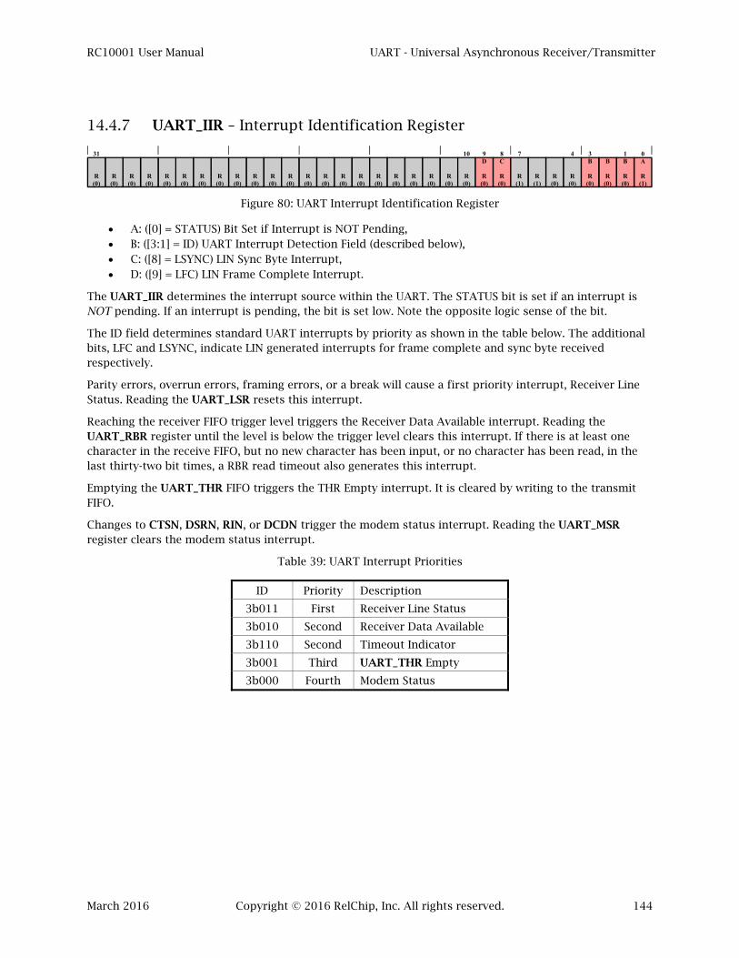
RC10001 User Manual UART - Universal Asynchronous Receiver/Transmitter
March 2016 Copyright © 2016 RelChip, Inc. All rights reserved. 144
14.4.7 UART_IIR – Interrupt Identification Register
Figure 80: UART Interrupt Identification Register
A: ([0] = STATUS) Bit Set if Interrupt is NOT Pending, B: ([3:1] = ID) UART Interrupt Detection Field (described below), C: ([8] = LSYNC) LIN Sync Byte Interrupt, D: ([9] = LFC) LIN Frame Complete Interrupt.
The UART_IIR determines the interrupt source within the UART. The STATUS bit is set if an interrupt is NOT pending. If an interrupt is pending, the bit is set low. Note the opposite logic sense of the bit.
The ID field determines standard UART interrupts by priority as shown in the table below. The additional bits, LFC and LSYNC, indicate LIN generated interrupts for frame complete and sync byte received respectively.
Parity errors, overrun errors, framing errors, or a break will cause a first priority interrupt, Receiver Line Status. Reading the UART_LSR resets this interrupt.
Reaching the receiver FIFO trigger level triggers the Receiver Data Available interrupt. Reading the UART_RBR register until the level is below the trigger level clears this interrupt. If there is at least one character in the receive FIFO, but no new character has been input, or no character has been read, in the last thirty-two bit times, a RBR read timeout also generates this interrupt.
Emptying the UART_THR FIFO triggers the THR Empty interrupt. It is cleared by writing to the transmit FIFO.
Changes to CTSN, DSRN, RIN, or DCDN trigger the modem status interrupt. Reading the UART_MSR register clears the modem status interrupt.
Table 39: UART Interrupt Priorities
ID Priority Description
3b011 First Receiver Line Status
3b010 Second Receiver Data Available
3b110 Second Timeout Indicator
3b001 Third UART_THR Empty
3b000 Fourth Modem Status
R(0)
R(0)
R(0)
R(0)
R(0)
R(0)
R(0)
R(0)
R(0)
R(0)
R(0)
R(0)
0A
R(1)
R(0)
R(0)
R(0)
R(0)
R(0)
R(0)
R(0)
R(0)
31
R(0)
10
R(0)
1B
R(0)
B
R(0)
3B
R(0)
8C
R(0)
9D
R(0)
7
R(1)
R(1)
R(0)
4
R(0)

RC10001 User Manual UART - Universal Asynchronous Receiver/Transmitter
March 2016 Copyright © 2016 RelChip, Inc. All rights reserved. 145
14.4.8 UART_LCR – Line Control Register
Figure 81: UART Line Control Register
A: ([1:0] = WLS) Word Length: Sets the word length from five to eight bits as per Table 40, B: ([2] = SBS) Number of Stop Bits. Low means one stop bit, and high means one and a half stop
bits, C: ([3] = PES) Parity Enable. Parity is enabled when set, D: ([4] = EPS) Even Parity Enable. When PES is high, EPS controls the parity sense. When not sticky,
EPS low means odd parity and high means even parity. When the sticky bit (SPS) is set, EPS low means parity is always high, while when it is high, parity is always low,
E: ([5] = SPS) Sticky Parity Enable. When set, the parity set with the PES and EPS bits is a fixed value, always low when PES and EPS are high, and always high when PES is high and EPS is low,
F: ([6] = BCS) Break Control Serial Output: In RS-232 mode, asserting this bit (high) forces the transmitter to a constant low output. In LIN mode, it is used to force a low out to generate a control-break sequence,
G: ([7] = DLAB) Register Address Pointer. When set, the UART_DLL and UART_DLM registers are available in the address space. When clear, the UART_RBR, UART_THR, and UART_IE registers are available,
H: ([8] = DIV8) Sample Divide by Eight Enable. When set, an eight cycle sample is used in the UART (baud = one eighth of the system clock maximum). Sixteen cycle samples is the default setting.
The UART_LCR controls data reception and transmission methods. It also contains the DLAB switch to select between registers in the UART address space. The table below decodes the bit meanings.
Table 40: UART Line Control Register Fields
Field Value Description
WLS 2b00 Word Length = 5 Bits
WLS 2b01 Word Length = 6 Bits
WLS 2b10 Word Length = 7 Bits
WLS 2b11 Word Length = 8 Bits
SBS 1b0 1 Stop Bit
SBS 1b1 1.5 Stop Bits
PES 1b0 No Parity
PES 1b1 Parity Enabled
BCS 1b0 Break Control Disable
BCS 1b1 Force Serial Out Low
DLAB 1b0 Normal Register Access
DLAB 1b1 UART_DLL/DLM Access
DIV8 1b0 BAUD Rate Divisor = 16
DIV8 1b1 BAUD Rate Divisor = 8
1A
RW(0)
R(0)
R(0)
R(0)
R(0)
R(0)
31
R(0)
R(0)
0A
RW(0)
R(0)
R(0)
R(0)
R(0)
R(0)
R(0)
R(0)
R(0)
R(0)
R(0)
R(0)
R(0)
R(0)
R(0)
R(0)
9
R(0)
7G
RW(0)
2B
RW(0)
3C
RW(0)
4D
RW(0)
5E
RW(0)
6F
RW(0)
8H
RW(0)

RC10001 User Manual UART - Universal Asynchronous Receiver/Transmitter
March 2016 Copyright © 2016 RelChip, Inc. All rights reserved. 146
Table 41: UART Line Control Register Parity Fields
EPS SPS Description
1b0 1b0 Odd Parity
1b0 1b1 High Parity
1b1 1b0 Even Parity
1b1 1b1 Low Parity
14.4.9 UART_MCR – Modem Control Register
Figure 82: UART Modem Control Register
A: ([0] = DTR) Drives the inverse of the DTRN pin logic level, B: ([1] = RTS) Drives the inverse of the RTSN pin logic level, C: ([2] = OUT1) Drives the OUT1 pin logic level, D: ([3] = OUT2) Drives the OUT2 pin logic level, E: ([4] = LB) Enable loopback test mode. In this mode, the TXD pin is set high and the internal TX
output connects to the internal RX channel. Also, DTRN connects to DSRN, RTSN connects to CTSN, OUT1Nconnects to RIN, and OUT2 connects to DCDN,
F: ([6] = Reserved) This bit must always be written low for proper UART operation, G: ([7] = CTSEN) Enable auto-CTS flow control when one. The transmitter will not send data unless
CTSN is low. If CTSN de-asserting before the middle of the next byte, the byte is not transmitted. A change to CTSN can cause an interrupt if enabled.
The modem control register controls the UART interface. Transmit and receive auto-flow control are enabled separately. Loopback is also controlled, and the output bits (OUT1, OUT2, RTSN, and DTRN) are set or cleared.
1B
RW(0)
R(0)
R(0)
R(0)
R(0)
R(0)
31
R(0)
R(0)
0A
RW(0)
R(0)
R(0)
R(0)
R(0)
R(0)
R(0)
R(0)
R(0)
R(0)
R(0)
R(0)
R(0)
R(0)
R(0)
R(0)
R(0)
7G
RW(0)
2C
RW(0)
3D
RW(0)
4E
RW(0)
6F
RW(0)
8
R(0)
5
R(0)
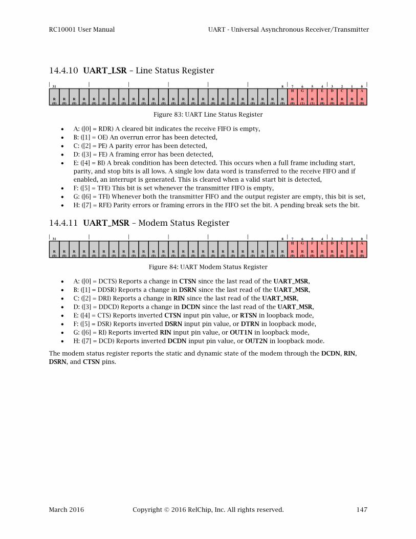
RC10001 User Manual UART - Universal Asynchronous Receiver/Transmitter
March 2016 Copyright © 2016 RelChip, Inc. All rights reserved. 147
14.4.10 UART_LSR – Line Status Register
Figure 83: UART Line Status Register
A: ([0] = RDR) A cleared bit indicates the receive FIFO is empty, B: ([1] = OE) An overrun error has been detected, C: ([2] = PE) A parity error has been detected, D: ([3] = FE) A framing error has been detected, E: ([4] = BI) A break condition has been detected. This occurs when a full frame including start,
parity, and stop bits is all lows. A single low data word is transferred to the receive FIFO and if enabled, an interrupt is generated. This is cleared when a valid start bit is detected,
F: ([5] = TFE) This bit is set whenever the transmitter FIFO is empty, G: ([6] = TFI) Whenever both the transmitter FIFO and the output register are empty, this bit is set, H: ([7] = RFE) Parity errors or framing errors in the FIFO set the bit. A pending break sets the bit.
14.4.11 UART_MSR – Modem Status Register
Figure 84: UART Modem Status Register
A: ([0] = DCTS) Reports a change in CTSN since the last read of the UART_MSR, B: ([1] = DDSR) Reports a change in DSRN since the last read of the UART_MSR, C: ([2] = DRI) Reports a change in RIN since the last read of the UART_MSR, D: ([3] = DDCD) Reports a change in DCDN since the last read of the UART_MSR, E: ([4] = CTS) Reports inverted CTSN input pin value, or RTSN in loopback mode, F: ([5] = DSR) Reports inverted DSRN input pin value, or DTRN in loopback mode, G: ([6] = RI) Reports inverted RIN input pin value, or OUT1N in loopback mode, H: ([7] = DCD) Reports inverted DCDN input pin value, or OUT2N in loopback mode.
The modem status register reports the static and dynamic state of the modem through the DCDN, RIN, DSRN, and CTSN pins.
R(0)
R(0)
R(0)
R(0)
R(0)
R(0)
R(0)
R(0)
R(0)
R(0)
R(0)
R(0)
0A
R(0)
R(0)
R(0)
R(0)
R(0)
R(0)
R(0)
R(0)
R(0)
31
R(0)
8
R(0)
1B
R(0)
2C
R(0)
3D
R(0)
6G
R(1)
7H
R(0)
5F
R(1)
4E
R(0)
R(0)
R(0)
R(0)
R(0)
R(0)
R(0)
R(0)
R(0)
R(0)
R(0)
R(0)
R(0)
R(0)
R(0)
0A
R(0)
R(0)
R(0)
R(0)
R(0)
R(0)
R(0)
R(0)
R(0)
31
R(0)
8
R(0)
1B
R(0)
2C
R(0)
3D
R(0)
6G
R(0)
7H
R(0)
5F
R(0)
4E
R(0)
R(0)
R(0)

RC10001 User Manual UART - Universal Asynchronous Receiver/Transmitter
March 2016 Copyright © 2016 RelChip, Inc. All rights reserved. 148
14.4.12 UART_SCR – Scratch Register
Figure 85: UART Scratch Register
A: ([7:0] = SCR) Scratch Data Register.
The scratch pad register is just what the name implies. Consistent with standard UART register, the register is eight-bits wide.
14.4.13 UART_TER – Transmit Enable Register
Figure 86: UART Transmit Enable Register
A: ([7] = TXEN) Transmitter is enabled by this bit.
The TXEN bit of this register controls transmission. When enabled, the transmitter will frame and send data from the FIFO. When clearing the bit, the current frame will complete before ending transmission.
14.4.14 UART_RS485CTRL – RS485 Control Register
Figure 87: UART RS485 Control Register
F: ([5] = OINV) Polarity Control. The direction control pin (see SEL) logic level is set. E: ([4] = DCTRL) Automatic direction control is on when this bit is high. The direction control pin
is determined by SEL, and the polarity of that pin is determined by OINV, D: ([3] = SEL) A low uses RTSN as the direction control pin, while a high uses DTRN. C: ([2] = AADEN) AADEN enables auto-address detection. Reception of a value with a parity error is
an address, without is data, B: ([1] = RXDIS) Receiver is disabled when this bit is high. When low, it is enabled, A: ([0] = NMMEN) Normal Multidrop Mode. The multidrop is used in conjunction with the address
detection,
This register configures the RS-485 interface. Auto direction control, auto address detection, and multidrop are all options. The receiver enable is also included.
A
RW(X)
R(0)
R(0)
R(0)
R(0)
R(0)
31
R(0)
R(0)
0A
RW(X)
R(0)
R(0)
R(0)
R(0)
R(0)
R(0)
R(0)
R(0)
R(0)
R(0)
R(0)
R(0)
R(0)
R(0)
R(0)
R(0)
8
R(0)
A
RW(X)
A
RW(X)
A
RW(X)
A
RW(X)
A
RW(X)
7A
RW(X)
R(0)
R(0)
R(0)
R(0)
R(0)
31
R(0)
R(0)
R(0)
R(0)
R(0)
R(0)
R(0)
R(0)
R(0)
R(0)
R(0)
R(0)
R(0)
R(0)
R(0)
R(0)
R(0)
R(0)
8
R(0)
7A
RW(0)
6
R(0)
R(0)
R(0)
R(0)
R(0)
R(0)
0
R(0)
1A
RW(0)
R(0)
R(0)
R(0)
R(0)
R(0)
31
R(0)
R(0)
0A
RW(0)
R(0)
R(0)
R(0)
R(0)
R(0)
R(0)
R(0)
R(0)
R(0)
R(0)
R(0)
R(0)
R(0)
R(0)
R(0)
R(0)
2B
RW(0)
3C
RW(0)
4D
RW(0)
6
R(0)
5E
RW(0)
R(0)
R(0)

RC10001 User Manual UART - Universal Asynchronous Receiver/Transmitter
March 2016 Copyright © 2016 RelChip, Inc. All rights reserved. 149
14.4.15 UART_RS485ADDR – RS485 Address Match Register
Figure 88: UART RS485 Address Register
A: ([7:0] = ADDR) The RS485 address is stored here.
The RS-485 address register contains the received address to check for an address match during auto address detection.
14.4.16 UART_RS485DLY – RS485 Turnaround Delay Register
Figure 89: UART RS485 Delay Register
A: ([7:0] = DLY) Turnaround delay.
The delay to turnaround the RS-485 connection is stored in this register.
14.4.17 UART_LCTL – LIN Control Register
Figure 90: UART LIN Control Register
A: ([0] = EN) Enables the LIN interface.
A
RW(0)
R(0)
R(0)
R(0)
R(0)
R(0)
31
R(0)
R(0)
0A
RW(0)
R(0)
R(0)
R(0)
R(0)
R(0)
R(0)
R(0)
R(0)
R(0)
R(0)
R(0)
R(0)
R(0)
R(0)
R(0)
R(0)
8
R(0)
A
RW(0)
A
RW(0)
A
RW(0)
A
RW(0)
A
RW(0)
7A
RW(0)
A
RW(0)
R(0)
R(0)
R(0)
R(0)
R(0)
31
R(0)
R(0)
0A
RW(0)
R(0)
R(0)
R(0)
R(0)
R(0)
R(0)
R(0)
R(0)
R(0)
R(0)
R(0)
R(0)
R(0)
R(0)
R(0)
R(0)
8
R(0)
A
RW(0)
A
RW(0)
A
RW(0)
A
RW(0)
A
RW(0)
7A
RW(0)
R(0)
R(0)
R(0)
R(0)
R(0)
31
R(0)
R(0)
0A
RW(0)
R(0)
R(0)
R(0)
R(0)
R(0)
R(0)
R(0)
R(0)
R(0)
R(0)
R(0)
R(0)
R(0)
R(0)
R(0)
R(0)
1
R(0)
R(0)
R(0)
R(0)
R(0)
R(0)
R(0)
R(0)

RC10001 User Manual SSP - Synchronous Serial Port
March 2016 Copyright © 2016 RelChip, Inc. All rights reserved. 150
15 SSP - SYNCHRONOUS SERIAL PORT
The SSP is a master or slave interface that enables synchronous serial communication with SPI-compatible devices. In both master and slave configurations the SSP performs:
Parallel-to-serial conversion on data written to an internal 16-bit wide, 8-location deep FIFO. Serial-to-parallel conversion on received data, buffering it in a similar 16-bit wide, 8-location deep
receive FIFO.
Possible interrupts are:
Request servicing of transmit and receive FIFOs. The receive FIFO has overrun (overflow). Data is present in the receive FIFO after an idle period has expired (stale data).
Features:
Master or slave operation. Full duplex, four-wire synchronous transfers. Programmable clock polarity and phase. Programmable clock bit rate and pre-scale. Separate transmit and receive first-in, first-out memory buffers, sixteen bits wide, eight words
deep. Programmable data frame size from four to sixteen bits. Independent masking of transmit FIFO, receive FIFO, and receive overrun interrupts. Internal loopback test mode available.
Transmission rates up to the clock divided by four are possible.
This peripheral requires the clock enable in SYSCON_AHBCLKCTRL - Clock Enable Register. At reset, the clock is disabled.
15.1 SIGNALS
The shared pin definitions are in Table 42.
Table 42: SSP Interface Signals
Pin SPI
Master SPI
Slave SSP uWIRE
Type Description
SCLK_GPIO0_0 SCLK SCLK CLK SK Out Serial Clock
MISO_GPIO0_1 MISO MOSI DR SI In Receive Data
MOSI_GPIO0_2 MOSI MISO DX SO Out Transmit Data
SSELA_GPIO0_3 SSELA SSEL FS CS Out Select A
SSELB_GPIO0_4 SSELB1 - - - Out Select B
SSELC_GPIO0_5 SSELC1 - - - Out Select C
SSELD_GPIO0_6 SSELD1 - - - Out Select D
Notes:
1. Not Used in Slave Mode
RC10001 User Manual SSP - Synchronous Serial Port
March 2016 Copyright © 2016 RelChip, Inc. All rights reserved. 151
15.2 INTERFACE PROTOCOLS
There are three possible serial protocols: serial peripheral interface (SPI), Texas Instrument Synchronous Serial Port (SSP), and Semiconductor Microwire.
All protocols transmit and receive the most-significant bit first as per industry standard.
Note that typical SPI Clock operation does not issue clocks on cycles not requiring data transfer. Therefore, SSELx and the clock issue during transmission cycles only. When the system SPI protocol requires half-duplex operation, the SPI interface must transmit and receive dummy data.
An example of SPI communication could require one byte with a data response of four bytes. To accomplish this, the SPI operates as follows:
1. Configuration: eight bit words. 2. Transmit an eight-bit command while receiving dummy data. 3. Receive four eight-bit data fields by transmitting four dummy bytes.
15.2.1 Serial Peripheral Interface Protocol
The SPI mode is a four-wire interface where the SSEL[A-D] signals behave as a select output. The RC10001 can also be a SPI slave to another system, using SSELA as the receiving select. Further, the SSEL[A-D] signal can be controlled in code as a GPIO pin. In this mode, groups of words can be transmitted while holding SSEL[A-D] constant. Figure 91 shows both options.
The inactive state and phase of the clock, SCLK, are configurable by the CPOL and CPHA bits in the SSP_CR0 register.
15.2.1.1 Clock Polarity (CPOL) and Phase (CPHA) control
CPOL determines the clock polarity: 0 = return-to-zero and 1 = return-to-one.
CPHA determines the active receiving clock edge: 0 = first edge and 1 = second edge. Data changes on the other clock edge.
The programmer can use automatic bounding of the SSEL signal (“FSS_SEL = 1” in Figure 91), or by programming the same pin as a GPIO pin.
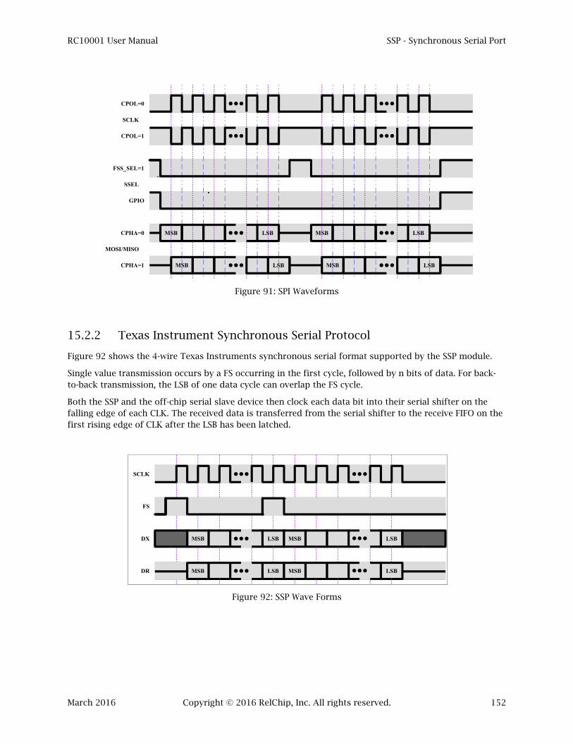
RC10001 User Manual SSP - Synchronous Serial Port
March 2016 Copyright © 2016 RelChip, Inc. All rights reserved. 152
Figure 91: SPI Waveforms
15.2.2 Texas Instrument Synchronous Serial Protocol
Figure 92 shows the 4-wire Texas Instruments synchronous serial format supported by the SSP module.
Single value transmission occurs by a FS occurring in the first cycle, followed by n bits of data. For back-to-back transmission, the LSB of one data cycle can overlap the FS cycle.
Both the SSP and the off-chip serial slave device then clock each data bit into their serial shifter on the falling edge of each CLK. The received data is transferred from the serial shifter to the receive FIFO on the first rising edge of CLK after the LSB has been latched.
Figure 92: SSP Wave Forms
CPOL=0
CPOL=1
FSS_SEL=1
GPIO
CPHA=0
CPHA=1
MSB
SCLK
SSEL
MOSI/MISO
MSB
LSB
LSB
MSB
MSB
LSB
LSB
SCLK
FS
DX
DR
MSB LSB MSB LSB
MSB LSB MSB LSB
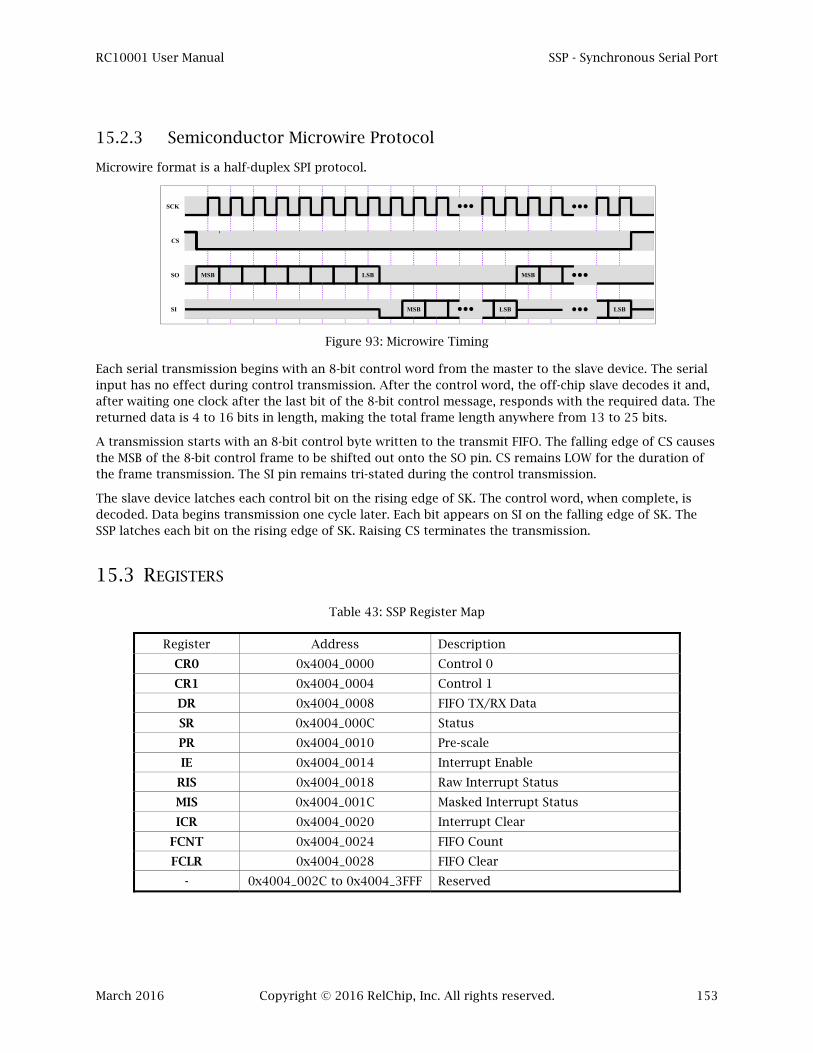
RC10001 User Manual SSP - Synchronous Serial Port
March 2016 Copyright © 2016 RelChip, Inc. All rights reserved. 153
15.2.3 Semiconductor Microwire Protocol
Microwire format is a half-duplex SPI protocol.
Figure 93: Microwire Timing
Each serial transmission begins with an 8-bit control word from the master to the slave device. The serial input has no effect during control transmission. After the control word, the off-chip slave decodes it and, after waiting one clock after the last bit of the 8-bit control message, responds with the required data. The returned data is 4 to 16 bits in length, making the total frame length anywhere from 13 to 25 bits.
A transmission starts with an 8-bit control byte written to the transmit FIFO. The falling edge of CS causes the MSB of the 8-bit control frame to be shifted out onto the SO pin. CS remains LOW for the duration of the frame transmission. The SI pin remains tri-stated during the control transmission.
The slave device latches each control bit on the rising edge of SK. The control word, when complete, is decoded. Data begins transmission one cycle later. Each bit appears on SI on the falling edge of SK. The SSP latches each bit on the rising edge of SK. Raising CS terminates the transmission.
15.3 REGISTERS
Table 43: SSP Register Map
Register Address Description
CR0 0x4004_0000 Control 0
CR1 0x4004_0004 Control 1
DR 0x4004_0008 FIFO TX/RX Data
SR 0x4004_000C Status
PR 0x4004_0010 Pre-scale
IE 0x4004_0014 Interrupt Enable
RIS 0x4004_0018 Raw Interrupt Status
MIS 0x4004_001C Masked Interrupt Status
ICR 0x4004_0020 Interrupt Clear
FCNT 0x4004_0024 FIFO Count
FCLR 0x4004_0028 FIFO Clear
- 0x4004_002C to 0x4004_3FFF Reserved
SCK
CS
SO
SI
MSB MSBLSB
MSB LSB LSB

RC10001 User Manual SSP - Synchronous Serial Port
March 2016 Copyright © 2016 RelChip, Inc. All rights reserved. 154
15.3.1 SSP_CR0 – Control 0 Register
Figure 94: SSP Control 0 Register
A: ([3:0] = DSS) Data size select is used to determine the width of a word. Values from three to fifteen are allowed and reflect data widths of four to sixteen (DSS + 1).
B: ([5:4] = FRF) The frame format selects the type of serial interface as follows: o 0: Serial Peripheral Interface, SPI o 1: Texas Instruments, TI o 2: Microwire o 3: Reserved
C: ([6] = CPOL) In SPI mode the clock polarity is set to 0, low between frames, or 1, high between frames. In all other SSP modes, the clock is low when not active.
D: ([7] = CPHA) In SPI mode the data is captured on the first edge of the clock when 0, or on the second edge of the clock when 1.
E: ([15:8] = SCR) Serial clock rate divisor (see below).
This register controls the number of bits per word (four to sixteen), the frame format, the clock polarity, the clock phase, and the serial clock rate (combined with the SSP_PR register).
R(0)
R(0)
R(0)
R(0)
R(0)
31
R(0)
R(0)
0A
RW(0)
R(0)
R(0)
R(0)
R(0)
R(0)
R(0)
R(0)
R(0)
16
R(0)
A
RW(0)
A
RW(0)
3A
RW(0)
4B
RW(0)
5B
RW(0)
6C
RW(0)
7D
RW(0)
8E
RW(0)
E
RW(0)
E
RW(0)
E
RW(0)
E
RW(0)
E
RW(0)
E
RW(0)
15E
RW(0)

RC10001 User Manual SSP - Synchronous Serial Port
March 2016 Copyright © 2016 RelChip, Inc. All rights reserved. 155
The serial clock rate is:
∗ 1
Where,
BAUD: the baud rate
PR: the pre-scale register value, (SSP_PR)
Fsspclk: The SSP clock frequency
15.3.2 SSP_CR1 – Control 1 Register
Figure 95: SSP Control 1 Register
A: ([0] = LBM) Loopback Test Mode Enable. When set, the transmit output is tied to the receiver input internally.
B: ([1] = SSE) Enable SSP. Writing a one to this bit enables the whole interface. All configurations will be set before writing this bit.
C: ([2] = MS) Master Slave Select. A zero sets a master interface. A one sets a slave interface. D: ([3] = SOD) Slave Output Disable. When set, the MISO output is tri-stated, allowing multiple
slaves with a common MISO. E: ([7:4] = FSS_SEL) Four slave selects (SSELA, SSELB, SSELC, and SSELD) enable are bits 4 through
7 (in order). A set bit allows a low transition during master operation. During slave operation, SSELA is the input select.
F: ([8] = SCKON) Enable Always-on serial clock. A low only outputs serial clocks when data is being output. A one outputs continuous serial clocks.
The second control register enables loop back mode, enables the SSP, configures the interface as a master or slave device, controls MISO output enable, enables the slave selects, and controls continuous SSP clock output.
R(0)
R(0)
R(0)
R(0)
R(0)
31
R(0)
R(0)
0A
RW(0)
R(0)
R(0)
R(0)
R(0)
R(0)
R(0)
R(0)
R(0)
R(0)
1B
RW(0)
2C
RW(0)
3D
RW(0)
4E
RW(0)
E
RW(0)
E
RW(0)
7E
RW(0)
8F
RW(0)
R(0)
R(0)
R(0)
R(0)
R(0)
R(0)
9
R(0)

RC10001 User Manual SSP - Synchronous Serial Port
March 2016 Copyright © 2016 RelChip, Inc. All rights reserved. 156
15.3.3 SSP_DR – FIFO TX/RX Data Registers
Figure 96: SSP FIFO TX/RX Data Registers
A: ([15:0] = TXFIFO) Data Entry Point for Transmitter FIFO (Write Only) B: ([15:0] = RXFIFO) Data Exit Point for Receiver FIFO (Read Only)
The SSP_DR data register reads from the receive FIFO. A write to this register writes data to the SSP Transmit FIFO. The SSP_FCLR register clears the FIFOs.
15.3.4 SSP_SR – Status Register
Figure 97: SSP Status Register
A: ([0] = TFE) When one, the transmit FIFO is empty, B: ([1] = TNF) When one, the transmit FIFO is not full, C: ([2] = RNE) When one, the receive FIFO is not empty, D: ([3] = RFF) When one, the receive FIFO is full, E: ([4] = BSY) When one, the SSP is currently transmitting and/or receiving a frame, or the transmit
FIFO is not empty.
The status register reports the current state of the FIFO and busy status.
15.3.5 SSP_PR – Pre-scale Register
Figure 98: SSP Pre-scale Register
A: ([7:0] = CNT) Pre-scale value.
Even numbers (2 to 254) programmed into this register are used to divide the system clock for the SPI interface.
B
R(X)
B
R(X)
B
R(X)
B
R(X)
B
R(X)
B
R(X)
B
R(X)
B
R(X)
B
R(X)
B
R(X)
B
R(X)
B
R(X)
B
R(X)
B
R(X)
B
R(X)
B
R(X)
31
R(0)
R(0)
R(0)
R(0)
R(0)
R(0)
R(0)
R(0)
R(0)
R(0)
R(0)
15A
W
A
W
A
W
A
W
A
W
A
W
A
W
A
W
A
W
A
W
A
W
A
W
A
W
A
W
A
W
0A
W
R(0)
R(0)
R(0)
R(0)
16
R(0)
R(0)
R(0)
R(0)
R(0)
R(0)
R(0)
R(0)
R(0)
R(0)
R(0)
R(0)
R(0)
0A
R(1)
R(0)
R(0)
R(0)
R(0)
R(0)
R(0)
R(0)
R(0)
31
R(0)
R(0)
1B
R(1)
2C
R(0)
3D
R(0)
4E
R(0)
R(0)
R(0)
R(0)
R(0)
5
R(0)
R(0)
R(0)
R(0)
R(0)
R(0)
31
R(0)
R(0)
0A
RW(1)
R(0)
R(0)
R(0)
R(0)
R(0)
R(0)
R(0)
R(0)
R(0)
A
RW(0)
A
RW(0)
A
RW(0)
A
RW(0)
A
RW(0)
A
RW(0)
7A
RW(0)
R(0)
R(0)
R(0)
R(0)
R(0)
R(0)
R(0)
8
R(0)

RC10001 User Manual SSP - Synchronous Serial Port
March 2016 Copyright © 2016 RelChip, Inc. All rights reserved. 157
15.3.6 SSP_IE - Interrupt Enable Register
Figure 99: SSP Interrupt Enable Register
A: ([0] = RORIE) Receive overrun interrupt enable. If the RX FIFO is written while it is full, a receive overrun condition is generated,
B: ([1] = RTIE) Receive FIFO read timeout interrupt enable. Not reading the RX FIFO for 32 bit times while it is not empty generates a RX FIFO read timeout interrupt,
C: ([2] = RXIE) Receive FIFO half-full interrupt enable. If the RX FIFO is half, or more than half, full, a RX FIFO half full condition is generated,
D: ([3] = TXIE) Transmit FIFO half-full interrupt enable. If the TX FIFO is half, or less than half, full, a TX FIFO half full condition is generated,
E: ([4] = ABIE) Cycle aborted interrupt enable. If a frame starts transmitting, but did not complete due to the select line taken high, the cycle aborted.
The interrupt enable selectively enables interrupt(s) for this interface. Setting a bit to one enables the interrupt.
15.3.7 SSP_RIS - Raw Interrupt Status Register
Figure 100: SSP Raw Interrupt Status Register
A: ([0] = RORIS) RX FIFO Overrun Condition, B: ([1] = RTRIS) RX FIFO Timeout Condition, C: ([2] = RXRIS) RX FIFO Half Full (or more) Condition, D: ([3] = TXRIS) TX FIFO Half Full (or less) Condition, E: ([4] = ABRIS) TX Cycle Aborted Condition.
The raw interrupt status is the pre-enable interrupt state.
R(0)
R(0)
R(0)
R(0)
R(0)
31
R(0)
R(0)
0A
RW(0)
R(0)
R(0)
R(0)
R(0)
R(0)
R(0)
R(0)
R(0)
R(0)
1B
RW(0)
2C
RW(0)
3D
RW(0)
4E
RW(0)
R(0)
R(0)
R(0)
R(0)
R(0)
R(0)
R(0)
R(0)
R(0)
R(0)
5
R(0)
R(0)
R(0)
R(0)
R(0)
R(0)
R(0)
R(0)
R(0)
R(0)
R(0)
R(0)
R(0)
0A
R(0)
R(0)
R(0)
R(0)
R(0)
R(0)
R(0)
R(0)
R(0)
31
R(0)
R(0)
1B
R(0)
2C
R(0)
3D
R(0)
4E
R(0)
R(0)
R(0)
R(0)
R(0)
5
R(0)

RC10001 User Manual SSP - Synchronous Serial Port
March 2016 Copyright © 2016 RelChip, Inc. All rights reserved. 158
15.3.8 SSP_MIS - Masked Interrupt Status Register
Figure 101: SSP Masked Interrupt Status Register
A: ([0] = ROMIS) RX FIFO Overrun Interrupt, B: ([1] = RTMIS) RX FIFO Timeout Interrupt, C: ([2] = RXMIS) RX FIFO Half Full (or more) Interrupt, D: ([3] = TXMIS) TX FIFO Half Full (or less) Interrupt, E: ([4] = ABMIS) TX Cycle Aborted Interrupt.
The masked interrupt status is the post-enable interrupt. It is the logical AND of the interrupt enable and the SSP_RIS register.
15.3.9 SSP_ICR - Interrupt Clear Register
Figure 102: SSP Interrupt Clear Register
A: ([0] = RORIC) Clear RX FIFO Overrun Interrupt. B: ([1] = RTRIC) Clear RX FIFO Timeout Interrupt. C: ([2] = ABRIC) Clear TX Cycle Aborted Interrupt.
The SSP_ICR register clears one or more interrupts by writing a one to the register.
15.3.10 SSP_FCNT – FIFO Count Register
Figure 103: SSP FIFO Count Register
A: ([3:0] = TX) Current Number of Entries in the TX FIFO, B: ([11:8] = RX) Current Number of Entries in the RX FIFO.
The FIFO count register contains the current number of entries in both receive and transmit FIFOs.
R(0)
R(0)
R(0)
R(0)
R(0)
R(0)
R(0)
R(0)
R(0)
R(0)
R(0)
R(0)
0A
R(0)
R(0)
R(0)
R(0)
R(0)
R(0)
R(0)
R(0)
R(0)
31
R(0)
R(0)
1B
R(0)
2C
R(0)
3D
R(0)
4E
R(0)
R(0)
R(0)
R(0)
R(0)
5
R(0)
31 0A
WP
5 3 2 1B
WP
4C
WP
R(0)
R(0)
R(0)
R(0)
R(0)
R(0)
R(0)
R(0)
R(0)
R(0)
12
R(0)
0A
R(X)
R(0)
R(0)
R(0)
R(0)
R(0)
R(0)
R(0)
R(0)
31
R(0)
7
R(0)
A
R(X)
A
R(X)
3A
R(X)
R(0)
R(0)
4
R(0)
8B
R(X)
B
R(X)
B
R(X)
11B
R(X)

RC10001 User Manual SSP - Synchronous Serial Port
March 2016 Copyright © 2016 RelChip, Inc. All rights reserved. 159
15.3.11 SSP_FCLR – FIFO Clear Register
Figure 104: SSP FIFO Clear Register
A: ([0] = TX) Clear the TX FIFO, B: ([1] = RX) Clear the RX FIFO.
The FIFO clear register clears all the entries in the FIFO(s). Current transmission of a word will complete.
31 0A
WP
2 1B
WP

RC10001 User Manual TIMER- Timer Counters
March 2016 Copyright © 2016 RelChip, Inc. All rights reserved. 160
16 TIMER- TIMER COUNTERS
There are four timer/counters in the RC10001, two sixteen bit and two thirty-two bit. These are named TIMER 16A, TIMER 16B, TIMER 32A, and TIMER 32B. Each timer/counter has four match outputs, and one capture input (see Table 44).
Table 44: Timer/Counter Pins
Signal TIMER 16A TIMER 16B
Capture T16ACAP0_GPIO0_7 T16BCAP0_GPIO1_0
Match 0 T16AMAT0_GPIO0_8 T16BMAT0_GPIO1_1
Match 1 T16AMAT1_GPIO0_9 T16BMAT1_GPIO1_2
Match 2 T16AMAT2_GPIO0_10 T16BMAT2_GPIO1_3
Match 3 T16AMAT3_GPIO0_11 T16BMAT3_GPIO1_4
Signal TIMER 32A TIMER 32B
Capture T32ACAP0_GPIO1_5 T32BCAP0_GPIO1_10
Match 0 T32AMAT0_GPIO1_6 T32BMAT0_GPIO1_11
Match 1 T32AMAT1_GPIO1_7 T32BMAT1_GPIO2_0
Match 2 T32AMAT2_GPIO1_8 T32BMAT2_GPIO2_1
Match 3 T32AMAT3_GPIO1_9 T32BMAT3_GPIO2_2
To read or write the counter registers, or operate the peripheral, set the appropriate clock bit in the SYSCON_AHBCLKCTRL - Clock Enable Register. Upon reset, these clocks are disabled.
The counter configuration includes enabling, reset, stop, and capture options. When enabled, the counter counts to an action threshold: stop, reset, and/or interrupt. The counter clock is the system clock divided by the pre-scale.
An event occurs on each match (MAT0 to MAT3). Matches with each channel create programmable signals at output pins. The capture input of each timer, CAP0, is optionally a clock input to the counter, or a trigger to capture the current timer value.
The counter clock source can be the system clock, the capture pin, or the UART RXD pin.
16.1 TIMER 16 VS TIMER 32
The difference between the sixteen bit and thirty-two bit timers is the size of the certain internal registers and counters. With the sixteen bit timer, the timer/counter (TIMER_TC), pre-scale compare (TIMER_PR), pre-scale counter (TIMER_PC), match (TIMER_MR[3:0]), and capture (TIMER_CR0) registers are sixteen bit. With the thirty-two bit timer, these registers are all thirty-two bit. Thus, the thirty-two bit timer counters have a much larger range (232 compared to 216). The total range for a counter, including pre-scale is 232 for the sixteen-bit timers, and 264 for the thirty-two bit counters.
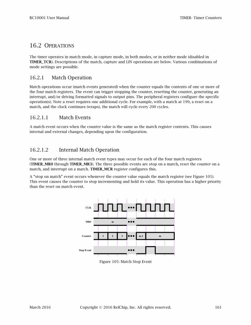
RC10001 User Manual TIMER- Timer Counters
March 2016 Copyright © 2016 RelChip, Inc. All rights reserved. 161
16.2 OPERATIONS
The timer operates in match mode, in capture mode, in both modes, or in neither mode (disabled in TIMER_TCR). Descriptions of the match, capture and LIN operations are below. Various combinations of mode settings are possible.
16.2.1 Match Operation
Match operations occur (match events generated) when the counter equals the contents of one or more of the four match registers. The event can trigger stopping the counter, resetting the counter, generating an interrupt, and/or driving formatted signals to output pins. The peripheral registers configure the specific operation(s). Note a reset requires one additional cycle. For example, with a match at 199, a reset on a match, and the clock continues (wraps), the match will cycle every 200 cycles.
16.2.1.1 Match Events
A match event occurs when the counter value is the same as the match register contents. This causes internal and external changes, depending upon the configuration.
16.2.1.2 Internal Match Operation
One or more of three internal match event types may occur for each of the four match registers (TIMER_MR0 through TIMER_MR3). The three possible events are stop on a match, reset the counter on a match, and interrupt on a match. TIMER_MCR register configures this.
A “stop on match” event occurs whenever the counter value equals the match register (see Figure 105). This event causes the counter to stop incrementing and hold its value. This operation has a higher priority than the reset on match event.
Figure 105: Match Stop Event
CLK
MR#
Counter
Stop Event
1 2 3 m-1 m
m

RC10001 User Manual TIMER- Timer Counters
March 2016 Copyright © 2016 RelChip, Inc. All rights reserved. 162
The “reset on match event” (see Figure 106) causes the counter (and pre-scale) to reset to zero. This is a single cycle event. The counter begins counting afterwards.
Figure 106: Match Reset Event
The “interrupt on match” event does not affect the counter. Whenever the match register equals the counter value, an interrupt will be generated (TIMER_IR register). An overall interrupt enable for the peripheral is available in the NVIC registers. The NVIC registers clear the interrupts. Thus, whenever the peripheral counter is enabled (CEN in TIMER_TCR), interrupts are enabled globally through the NVIC register, and selectively by the “interrupt on match” enables in the TIMER_MCR register.
Figure 107: Match Interrupt Event
CLK
MR#
Counter
Stop Event
1 2 3 m-1 m
m
0 1
CLK
MR#
Counter
Stop Event
1 2 3 m-1 m
m
m+1 m+2

RC10001 User Manual TIMER- Timer Counters
March 2016 Copyright © 2016 RelChip, Inc. All rights reserved. 163
16.2.1.3 External Match Operation
Match operations can also directly time external operations. Figure 108 depicts the equivalent circuit. emr# and pwm# are set and cleared by matches configured in the TIMER_PWMC register.
Figure 108: Match Output Circuit (MAT0)
Matches generate external signal edges as shown in Figure 109. The matches generate the internal signals emr and pwm. Four different match registers drive various external signal formats. In the example below, one match register generates a reset count, n, while the “m match” denotes any one of the three remaining match registers. Configuration in the TIMER_EMR register configures the match to 1. Do nothing, 2. Set the output high, 3. Set the output low, or 4. Toggle the output. The signals, emr and pwm, then format the output signal.
Figure 109: External Match and PWM Generation
CLK
MR#
Counter
PWM
1 2 3 m-1 m
m
m+1
nMR#
SET 1
SET 0
TOGGLE
m+2 n-1 n 0 1

RC10001 User Manual TIMER- Timer Counters
March 2016 Copyright © 2016 RelChip, Inc. All rights reserved. 164
16.2.2 Capture Operation
The timer peripheral can capture counts on external events. The captured event is a rising edge, falling edge, or either edge. When the event occurs, the value of the counter is stored in the capture value register (TIMER_CR0). This capture event can also cause the counter to reset if so configured.
The count control register (TIMER_CTCR) configures the clock input. One option is to use the capture pin as the clock input. The internal clock samples the capture pin to synchronize it. Thus, the capture clock must operate at less than one-half the system clock.
16.2.3 UART/LIN Counter Mode
The RXD pin can be connected to TIMER 32A as the clock for the counter when set in the TIMER_CTCR register. This is then used to auto-baud detect by detecting the time between two specific edges of the RXD pin. The extra byte at an unknown baud causes no issues if the UART is set to loopback mode during detection.

RC10001 User Manual TIMER- Timer Counters
March 2016 Copyright © 2016 RelChip, Inc. All rights reserved. 165
16.3 REGISTERS
Table 45 shows the timer/counter registers. The “?_?” field in the address determines which timer is used as follows:
0_C: TIMER 16A 1_0: TIMER 16B 1_4: TIMER 32A 1_8: TIMER 32B
Table 45: Timer Register Addressing
Register Address Description
IR 0x400?_?000 Interrupts
TCR 0x400?_?004 Timer Control
TC 0x400?_?008 Timer Counter Value
PR 0x400?_?00C Pre-scale Compare
PC 0x400?_?010 Pre-scale Counter
MCR 0x400?_?014 Match Control
MR0 0x400?_?018 Match
MR1 0x400?_?01C Match
MR2 0x400?_?020 Match
MR3 0x400?_?024 Match
CCR 0x400?_?028 Capture Control
CR0 0x400?_?02C Capture Value
- 0x400?_?030 to 0x400?_?03B Reserved
EMR 0x400?_?03C External Match
- 0x400?_?040 to 0x400?_?06F Reserved
CTCR 0x400?_?070 Count Control
PWMC 0x400?_?074 PWM Control
MOCR 0x400?_?078 Match Output Control
MOR 0x400?_?07C Match Output
- 0x400?_?080 to 0x400?_?FFF Reserved

RC10001 User Manual TIMER- Timer Counters
March 2016 Copyright © 2016 RelChip, Inc. All rights reserved. 166
16.3.1 TIMER_IR – Interrupt Register
Figure 110: TIMER Interrupt Register
A: ([0] = MR0) Match 0 Interrupt Status and Clear. A read will report the status of the match 0 interrupt. Writing a one will clear the interrupt,
B: ([1] = MR1) Match 1 Interrupt Status and Clear. A read will report the status of the match 1 interrupt. Writing a one will clear the interrupt,
C: ([2] = MR2) Match 2 Interrupt Status and Clear. A read will report the status of the match 2 interrupt. Writing a one will clear the interrupt,
D: ([3] = MR3) Match 3 Interrupt Status and Clear. A read will report the status of the match 3 interrupt. Writing a one will clear the interrupt,
E: ([4] = CAP) Capture Interrupt Status and Clear. A read will report the status of the capture interrupt. Writing a one will clear the interrupt.
This register reports and clears five interrupts. Upon an interrupt for one of the functions, the appropriate bit will be set high. When written by the processor, a one will reset the interrupt.
16.3.2 TIMER_TCR – Timer Control Register
Figure 111: TIMER Control Register
A: ([0] = CEN) Counter Enable: Enables the counter, B: ([1] = CRST) Counter Reset: When written high, the counter is held in reset.
The timer control register enables the internal counter and pre-scale counter (CEN high). The counters will be reset (and remain in reset) whenever the CRST bit is set high. A low CRST bit allows CEN to control the counter.
A
R(0)
B
R(0)
C
R(0)
D
R(0)
E
R(0)
31
R(0)
R(0)
R(0)
R(0)
R(0)
R(0)
R(0)
R(0)
R(0)
R(0)
R(0)
4E
WP
3D
WP
2C
WP
1B
WP
0A
WP
R(0)
R(0)
R(0)
R(0)
R(0)
R(0)
R(0)
R(0)
R(0)
R(0)
R(0)
R(0)
R(0)
R(0)
R(0)
5
R(0)
R(0)
R(0)
R(0)
R(0)
R(0)
31
R(0)
R(0)
0A
RW(0)
R(0)
R(0)
R(0)
R(0)
R(0)
R(0)
R(0)
R(0)
R(0)
1B
RW(0)
R(0)
R(0)
R(0)
R(0)
R(0)
R(0)
R(0)
R(0)
R(0)
R(0)
R(0)
R(0)
R(0)
2
R(0)
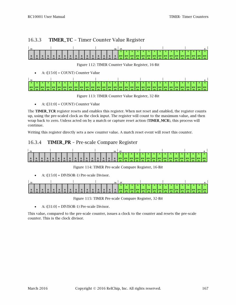
RC10001 User Manual TIMER- Timer Counters
March 2016 Copyright © 2016 RelChip, Inc. All rights reserved. 167
16.3.3 TIMER_TC – Timer Counter Value Register
Figure 112: TIMER Counter Value Register, 16-Bit
A: ([15:0] = COUNT) Counter Value
Figure 113: TIMER Counter Value Register, 32-Bit
A: ([31:0] = COUNT) Counter Value
The TIMER_TCR register resets and enables this register. When not reset and enabled, the register counts up, using the pre-scaled clock as the clock input. The register will count to the maximum value, and then wrap back to zero. Unless acted on by a match or capture reset action (TIMER_MCR), this process will continue.
Writing this register directly sets a new counter value. A match reset event will reset this counter.
16.3.4 TIMER_PR – Pre-scale Compare Register
Figure 114: TIMER Pre-scale Compare Register, 16-Bit
A: ([15:0] = DIVISOR-1) Pre-scale Divisor.
Figure 115: TIMER Pre-scale Compare Register, 32-Bit
A: ([31:0] = DIVISOR-1) Pre-scale Divisor.
This value, compared to the pre-scale counter, issues a clock to the counter and resets the pre-scale counter. This is the clock divisor.
R(0)
R(0)
R(0)
R(0)
R(0)
31
R(0)
R(0)
0A
RW(0)
R(0)
R(0)
R(0)
R(0)
R(0)
R(0)
R(0)
R(0)
16
R(0)
A
RW(0)
A
RW(0)
A
RW(0)
A
RW(0)
A
RW(0)
A
RW(0)
A
RW(0)
A
RW(0)
A
RW(0)
A
RW(0)
A
RW(0)
A
RW(0)
A
RW(0)
A
RW(0)
15A
RW(0)
0A
RW(0)
A
RW(0)
A
RW(0)
A
RW(0)
A
RW(0)
A
RW(0)
A
RW(0)
A
RW(0)
A
RW(0)
A
RW(0)
A
RW(0)
A
RW(0)
A
RW(0)
A
RW(0)
A
RW(0)
A
RW(0)
A
RW(0)
A
RW(0)
A
RW(0)
A
RW(0)
A
RW(0)
A
RW(0)
A
RW(0)
A
RW(0)
A
RW(0)
A
RW(0)
A
RW(0)
A
RW(0)
A
RW(0)
A
RW(0)
A
RW(0)
31A
RW(0)
R(0)
R(0)
R(0)
R(0)
R(0)
31
R(0)
R(0)
0A
RW(0)
R(0)
R(0)
R(0)
R(0)
R(0)
R(0)
R(0)
R(0)
16
R(0)
A
RW(0)
A
RW(0)
A
RW(0)
A
RW(0)
A
RW(0)
A
RW(0)
A
RW(0)
A
RW(0)
A
RW(0)
A
RW(0)
A
RW(0)
A
RW(0)
A
RW(0)
A
RW(0)
15A
RW(0)
R(0)
R(0)
R(0)
R(0)
R(0)
31
R(0)
R(0)
0A
RW(0)
R(0)
R(0)
R(0)
R(0)
R(0)
R(0)
R(0)
R(0)
16
R(0)
A
RW(0)
A
RW(0)
A
RW(0)
A
RW(0)
A
RW(0)
A
RW(0)
A
RW(0)
A
RW(0)
A
RW(0)
A
RW(0)
A
RW(0)
A
RW(0)
A
RW(0)
A
RW(0)
15A
RW(0)

RC10001 User Manual TIMER- Timer Counters
March 2016 Copyright © 2016 RelChip, Inc. All rights reserved. 168
16.3.5 TIMER_PC – Pre-scale Counter Register
Figure 116: TIMER Pre-scale Counter Register, 16-Bit
A: ([15:0] = COUNT) Current Pre-scale Count.
Figure 117: TIMER Pre-scale Counter Register, 32-Bit
A: ([31:0] = COUNT) Current Pre-scale Count.
The TIMER_TCR register resets and enables the pre-scale counter. When not reset and enabled, the register counts up using the system clock. The register will count until the value equals the pre-scale compare register (TIMER_PR). It will then issue one clock to the counter register.
Writing this register causes an immediate change to the value. A match reset event resets this register.
R(0)
R(0)
R(0)
R(0)
R(0)
31
R(0)
R(0)
0A
RW(0)
R(0)
R(0)
R(0)
R(0)
R(0)
R(0)
R(0)
R(0)
16
R(0)
A
RW(0)
A
RW(0)
A
RW(0)
A
RW(0)
A
RW(0)
A
RW(0)
A
RW(0)
A
RW(0)
A
RW(0)
A
RW(0)
A
RW(0)
A
RW(0)
A
RW(0)
A
RW(0)
15A
RW(0)
0A
RW(0)
A
RW(0)
A
RW(0)
A
RW(0)
A
RW(0)
A
RW(0)
A
RW(0)
A
RW(0)
A
RW(0)
A
RW(0)
A
RW(0)
A
RW(0)
A
RW(0)
A
RW(0)
A
RW(0)
A
RW(0)
A
RW(0)
A
RW(0)
A
RW(0)
A
RW(0)
A
RW(0)
A
RW(0)
A
RW(0)
A
RW(0)
A
RW(0)
A
RW(0)
A
RW(0)
A
RW(0)
A
RW(0)
A
RW(0)
A
RW(0)
31A
RW(0)

RC10001 User Manual TIMER- Timer Counters
March 2016 Copyright © 2016 RelChip, Inc. All rights reserved. 169
16.3.6 TIMER_MCR – Match Control Register
Figure 118: TIMER Match Control Register
A: ([0] = MR0I) Interrupt on match 0, B: ([1] = MR0R) Reset the Counter on match 0, C: ([2] = MR0S) Stop Counting on match 0, D: ([0] = MR1I) Interrupt on match 1, E: ([1] = MR1R) Reset the Counter on match 1, F: ([2] = MR1S) Stop Counting on match 1, G: ([0] = MR2I) Interrupt on match 2, H: ([1] = MR2R) Reset the Counter on match 2, I: ([2] = MR2S) Stop Counting on match 2, J: ([0] = MR3I) Interrupt on match 3, K: ([1] = MR3R) Reset the Counter on match 3, L: ([2] = MR3S) Stop Counting on match 3.
This register defines what happens when one of the match registers (TIMER_MR[3:0]) equals the timer counter (TIMER_TC). The programmer can ignore the match, or take action. The action can be generate an interrupt (MR0I, MR1I, MR2I, and MR3I), reset the timer counter (MR0R, MR1R, MR2R, and MR3R), or stop the timer counter (MR0S, MR1S, MR2S, MR3S). Combinations of these actions are allowed. For example if TIMER_MR[0] equals TIMER_TC, and all three bits (MR0I, MR0R, MR0S) are high, the timer will stop the timer counter, not reset the timer counter (only because stop has a higher priority), and issue an interrupt.
While the interrupt bit operates independently of the other two conditions, the stop bit has priority over the reset bit. Thus, if both are set, the counter will stop on the match count. Once the stop on match is cleared, the counter will reset on the next clock.
R(0)
R(0)
R(0)
R(0)
R(0)
31
R(0)
R(0)
0A
RW(0)
R(0)
R(0)
R(0)
R(0)
R(0)
R(0)
R(0)
R(0)
1B
RW(0)
2C
RW(0)
3D
RW(0)
4E
RW(0)
5F
RW(0)
6G
RW(0)
7H
RW(0)
8I
RW(0)
9J
RW(0)
10K
RW(0)
11L
RW(0)
R(0)
R(0)
R(0)
R(0)
12
R(0)

RC10001 User Manual TIMER- Timer Counters
March 2016 Copyright © 2016 RelChip, Inc. All rights reserved. 170
16.3.7 TIMER_MR# – Match Registers
Figure 119: TIMER Match Registers, 16-Bit
A: ([15:0] = COUNT) Match Value
Figure 120: TIMER Match Registers, 32-Bit
A: ([31:0] = COUNT) Match Value
The match registers save values to compare to the timer counter (TIMER_TC). TIMER_MCR and TIMER_MOCR registers determine the action taken.
16.3.8 TIMER_CCR – Capture Control Register
Figure 121: TIMER Capture Control Register
A: ([0] = RE) Capture the TIMER_TC value into the capture value register (TIMER_CR0) on the rising edge of the capture pin,
B: ([1] = FE) Capture the TIMER_TC value into the capture value register (TIMER_CR0) on the falling edge of the capture pin,
C: ([2] = I) Interrupt on a capture event, D: ([4] = ROC) Reset the TIMER_TC and TIMER_PC on a capture event.
The capture control register controls resetting on a capture event, interrupting on a capture, and defining the edge of a capture event.
R(0)
R(0)
R(0)
R(0)
R(0)
31
R(0)
R(0)
0A
RW(0)
R(0)
R(0)
R(0)
R(0)
R(0)
R(0)
R(0)
R(0)
16
R(0)
A
RW(0)
A
RW(0)
A
RW(0)
A
RW(0)
A
RW(0)
A
RW(0)
A
RW(0)
A
RW(0)
A
RW(0)
A
RW(0)
A
RW(0)
A
RW(0)
A
RW(0)
A
RW(0)
15A
RW(0)
0A
RW(0)
A
RW(0)
A
RW(0)
A
RW(0)
A
RW(0)
A
RW(0)
A
RW(0)
A
RW(0)
A
RW(0)
A
RW(0)
A
RW(0)
A
RW(0)
A
RW(0)
A
RW(0)
A
RW(0)
A
RW(0)
A
RW(0)
A
RW(0)
A
RW(0)
A
RW(0)
A
RW(0)
A
RW(0)
A
RW(0)
A
RW(0)
A
RW(0)
A
RW(0)
A
RW(0)
A
RW(0)
A
RW(0)
A
RW(0)
A
RW(0)
31A
RW(0)
R(0)
R(0)
R(0)
R(0)
R(0)
31
R(0)
R(0)
0A
RW(0)
R(0)
R(0)
R(0)
R(0)
R(0)
R(0)
R(0)
R(0)
1B
RW(0)
2C
RW(0)
4D
RW(0)
R(0)
R(0)
R(0)
R(0)
R(0)
R(0)
R(0)
R(0)
R(0)
R(0)
R(0)
5
R(0)
3
R(0)
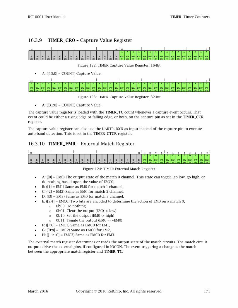
RC10001 User Manual TIMER- Timer Counters
March 2016 Copyright © 2016 RelChip, Inc. All rights reserved. 171
16.3.9 TIMER_CR0 – Capture Value Register
Figure 122: TIMER Capture Value Register, 16-Bit
A: ([15:0] = COUNT) Capture Value.
Figure 123: TIMER Capture Value Register, 32-Bit
A: ([31:0] = COUNT) Capture Value.
The capture value register is loaded with the TIMER_TC count whenever a capture event occurs. That event could be either a rising edge or falling edge, or both, on the capture pin as set in the TIMER_CCR register.
The capture value register can also use the UART’s RXD as input instead of the capture pin to execute auto-baud detection. This is set in the TIMER_CTCR register.
16.3.10 TIMER_EMR – External Match Register
Figure 124: TIMER External Match Register
A: ([0] = EM0) The output state of the match 0 channel. This state can toggle, go low, go high, or do nothing based upon the value of EMC0,
B: ([1] = EM1) Same as EM0 for match 1 channel, C: ([2] = EM2) Same as EM0 for match 2 channel, D: ([3] = EM3) Same as EM0 for match 3 channel, E: ([5:4] = EMC0) Two bits are encoded to determine the action of EM0 on a match 0,
o 0b00: Do nothing o 0b01: Clear the output (EM0 -> low) o 0b10: Set the output (EM0 -> high) o 0b11: Toggle the output (EM0 -> ~EM0)
F: ([7:6] = EMC1) Same as EMC0 for EM1, G: ([9:8] = EMC2) Same as EMC0 for EM2, H: ([11:10] = EMC3) Same as EMC0 for EM3.
The external match register determines or reads the output state of the match circuits. The match circuit outputs drive the external pins, if configured in IOCON. The event triggering a change is the match between the appropriate match register and TIMER_TC.
R(0)
R(0)
R(0)
R(0)
R(0)
31
R(0)
R(0)
0A
RW(0)
R(0)
R(0)
R(0)
R(0)
R(0)
R(0)
R(0)
R(0)
16
R(0)
A
RW(0)
A
RW(0)
A
RW(0)
A
RW(0)
A
RW(0)
A
RW(0)
A
RW(0)
A
RW(0)
A
RW(0)
A
RW(0)
A
RW(0)
A
RW(0)
A
RW(0)
A
RW(0)
15A
RW(0)
0A
RW(0)
A
RW(0)
A
RW(0)
A
RW(0)
A
RW(0)
A
RW(0)
A
RW(0)
A
RW(0)
A
RW(0)
A
RW(0)
A
RW(0)
A
RW(0)
A
RW(0)
A
RW(0)
A
RW(0)
A
RW(0)
A
RW(0)
A
RW(0)
A
RW(0)
A
RW(0)
A
RW(0)
A
RW(0)
A
RW(0)
A
RW(0)
A
RW(0)
A
RW(0)
A
RW(0)
A
RW(0)
A
RW(0)
A
RW(0)
A
RW(0)
31A
RW(0)
R(0)
R(0)
R(0)
R(0)
R(0)
31
R(0)
R(0)
0A
RW(0)
R(0)
R(0)
R(0)
R(0)
R(0)
R(0)
R(0)
R(0)
1B
RW(0)
2C
RW(0)
3D
RW(0)
R(0)
R(0)
R(0)
R(0)
12
R(0)
4E
RW(0)
5E
RW(0)
6F
RW(0)
7F
RW(0)
8G
RW(0)
9G
RW(0)
10H
RW(0)
11H
RW(0)

RC10001 User Manual TIMER- Timer Counters
March 2016 Copyright © 2016 RelChip, Inc. All rights reserved. 172
16.3.11 TIMER_CTCR – Count Control Register
Figure 125: TIMER Count Control Register
A: ([1:0] = CTM) Counter-Timer Mode, B: ([2] = AUTO) Capture Pin or Auto Baud Detect with RxD Pin.
There are two primary modes for timer interface, timer and counter. The timer uses the system clock to increment the pre-scale and TIMER_TC. In the counter modes, the UART RXD pin becomes the clock input for the pre-scale and TIMER_TC. When AUTO is set, the clock input is the UART’s RXD pin All clocks are internally generated by sampling with the system clock. Thus, any input clock frequency may not exceed one-half of the system clock.
The CTM field selects the source and edge to use. These are:
0b00: Timer mode using the system clock, 0b01: Counter mode using the rising edge of the capture pin or the UART RXD pin. 0b10: Counter mode using the falling edge of the capture pin or the UART RXD pin. 0b11: Counter mode using both edges of the capture pin or the UART RXD pin.
LIN mode uses the auto-baud detect of TIMER 32A and the UART interface.
16.3.12 TIMER_PWMC – Pulse Width Modulator Control Register
Figure 126: TIMER Pulse Width Modulator Control Register
A: ([0] = EN0) Enable pulse width modulation output on match pin 0, B: ([1] = EN1) Enable pulse width modulation output on match pin 1, C: ([2] = EN2) Enable pulse width modulation output on match pin 2, D: ([3] = EN3) Enable pulse width modulation output on match pin 3.
If a pulse width modulated enable bit is low, the EM output (TIMER_EMR) will appear on the match output pin. When high, the output will become a PWM output. A match on a channel will cause the output pin to go high. When the timer resets, the output will go low. This mode then supersedes match event (EM) channel values going to the output pins (see Figure 108).
To enable the PWMC mode, the appropriate field of the TIMER_EMR register must set (0b01) on a match.
R(0)
R(0)
R(0)
R(0)
R(0)
31
R(0)
R(0)
0A
RW(0)
R(0)
R(0)
R(0)
R(0)
R(0)
R(0)
R(0)
R(0)
1A
RW(0)
2B
RW(0)
R(0)
R(0)
R(0)
R(0)
R(0)
R(0)
R(0)
R(0)
R(0)
R(0)
R(0)
R(0)
R(0)
3
R(0)
R(0)
R(0)
R(0)
R(0)
R(0)
31
R(0)
R(0)
0A
RW(0)
R(0)
R(0)
R(0)
R(0)
R(0)
R(0)
R(0)
R(0)
1B
RW(0)
2C
RW(0)
R(0)
R(0)
R(0)
R(0)
R(0)
R(0)
R(0)
R(0)
R(0)
R(0)
R(0)
R(0)
4
R(0)
3D
RW(0)

RC10001 User Manual TIMER- Timer Counters
March 2016 Copyright © 2016 RelChip, Inc. All rights reserved. 173
16.3.13 TIMER_MOCR – Match Output Control Register
Figure 127: TIMER Match Output Control Register
A: ([0] = INV0) Invert match channel 0 just prior to leaving the circuit when set, B: ([1] = INV1) Invert match channel 1 just prior to leaving the circuit when set, C: ([2] = INV2) Invert match channel 2 just prior to leaving the circuit when set, D: ([3] = INV3) Invert match channel 3 just prior to leaving the circuit when set, E: ([4] = X01) Perform an exclusive-or of channels 0 and 1, invert channel 1, and present the
signals to the inverters (INV0, INV1 of Figure 108), F: ([5] = X23) Perform an exclusive-or of channels 2 and 3, invert channel 3, and present the
signals to the inverters (INV2, INV3).
The PWM stage process all four match events for external presentation. This allows exclusive-or connections, creating non-overlapping signal outputs, and selectable signal inversion.
16.3.14 TIMER_MOR – Match Output Register
Figure 128: TIMER Match Output Register
A: ([3:0] = MAT) The Four Match Occurred Results, B: ([4] = CAP) Capture Occurred.
The read-only match output register contains the values for match and capture signals in the peripheral after all logical manipulations (such as PWM, inversion, exclusive-or), but before the signals are applied to the pins. Thus, a “loopback” of all the logical changes is visible to code.
R(0)
R(0)
R(0)
R(0)
R(0)
31
R(0)
R(0)
0A
RW(0)
R(0)
R(0)
R(0)
R(0)
R(0)
R(0)
R(0)
R(0)
1B
RW(0)
2C
RW(0)
R(0)
R(0)
R(0)
R(0)
R(0)
R(0)
R(0)
R(0)
R(0)
R(0)
6
R(0)
3D
RW(0)
4E
RW(0)
5F
RW(0)
R(0)
R(0)
R(0)
R(0)
R(0)
R(0)
R(0)
R(0)
R(0)
R(0)
R(0)
R(0)
0A
R(0)
R(0)
R(0)
R(0)
R(0)
R(0)
R(0)
R(0)
R(0)
31
R(0)
R(0)
1A
R(0)
2A
R(0)
3A
R(0)
4B
R(0)
R(0)
R(0)
R(0)
R(0)
5
R(0)
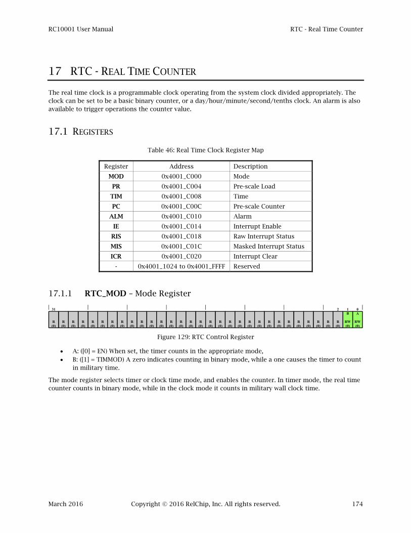
RC10001 User Manual RTC - Real Time Counter
March 2016 Copyright © 2016 RelChip, Inc. All rights reserved. 174
17 RTC - REAL TIME COUNTER
The real time clock is a programmable clock operating from the system clock divided appropriately. The clock can be set to be a basic binary counter, or a day/hour/minute/second/tenths clock. An alarm is also available to trigger operations the counter value.
17.1 REGISTERS
Table 46: Real Time Clock Register Map
Register Address Description
MOD 0x4001_C000 Mode
PR 0x4001_C004 Pre-scale Load
TIM 0x4001_C008 Time
PC 0x4001_C00C Pre-scale Counter
ALM 0x4001_C010 Alarm
IE 0x4001_C014 Interrupt Enable
RIS 0x4001_C018 Raw Interrupt Status
MIS 0x4001_C01C Masked Interrupt Status
ICR 0x4001_C020 Interrupt Clear
- 0x4001_1024 to 0x4001_FFFF Reserved
17.1.1 RTC_MOD – Mode Register
Figure 129: RTC Control Register
A: ([0] = EN) When set, the timer counts in the appropriate mode, B: ([1] = TIMMOD) A zero indicates counting in binary mode, while a one causes the timer to count
in military time.
The mode register selects timer or clock time mode, and enables the counter. In timer mode, the real time counter counts in binary mode, while in the clock mode it counts in military wall clock time.
R(0)
R(0)
R(0)
R(0)
R(0)
31
R(0)
R(0)
0A
RW(0)
R(0)
R(0)
R(0)
R(0)
R(0)
R(0)
R(0)
R(0)
1B
RW(0)
R(0)
R(0)
R(0)
R(0)
R(0)
R(0)
R(0)
R(0)
R(0)
R(0)
R(0)
R(0)
R(0)
R(0)
2
R(0)

RC10001 User Manual RTC - Real Time Counter
March 2016 Copyright © 2016 RelChip, Inc. All rights reserved. 175
17.1.2 RTC_PR – Pre-scale Load Register
Figure 130: RTC Pre-scale Load Register
A: ([23:0] = CNT) Pre-scale count.
The pre-scale load register is a twenty-four bit register to divide the system clock. It is set to 0x0C_3500 or 800,000 on reset. This value runs twice as fast as the clock at 4MHz (i.e. 1 second of clock time recorded every ½ second of real time). The user should program the correct value for the crystal used.
17.1.3 RTC_TIM – Time Register
Figure 131: RTC Time Register (Binary)
A: ([31:0] = CNT) Count Value.
Figure 132: RTC Time Register (Military Time Mode)
A: ([3:0] = MS) Counter for 0 to 9 0.1 seconds (100ms), B: ([9:4] = SEC) Counter for 0 to 59 seconds, C: ([15:10] = MIN) Counter for 0 to 59 minutes, D: ([20:16] = HR) Counter for 0 to 23 hours, E: ([31:21] = DAY) Counter for 0 to 2047 days. After 2047, the day count wraps back to zero.
The time register contains the current time as previously configured. Each clock tick (divided by the pre-scale) increments register. In binary mode, the register is a simple thirty-two bit counter. In time mode, the correct carry values are incremented.
R(0)
R(0)
R(0)
R(0)
R(0)
31
R(0)
R(0)
0A
RW(0)
24
R(0)
A
RW(0)
A
RW(0)
A
RW(0)
A
RW(0)
A
RW(0)
A
RW(0)
A
RW(0)
A
RW(1)
A
RW(0)
A
RW(1)
A
RW(0)
A
RW(1)
A
RW(1)
A
RW(0)
A
RW(0)
A
RW(0)
A
RW(0)
A
RW(1)
A
RW(1)
A
RW(0)
A
RW(0)
A
RW(0)
23A
RW(0)
0A
RW(0)
A
RW(0)
A
RW(0)
A
RW(0)
A
RW(0)
A
RW(0)
A
RW(0)
A
RW(0)
A
RW(0)
A
RW(0)
A
RW(0)
A
RW(0)
A
RW(0)
A
RW(0)
A
RW(0)
A
RW(0)
A
RW(0)
A
RW(0)
A
RW(0)
A
RW(0)
A
RW(0)
A
RW(0)
A
RW(0)
A
RW(0)
A
RW(0)
31A
RW(0)
A
RW(0)
A
RW(0)
A
RW(0)
A
RW(0)
A
RW(0)
A
RW(0)
0A
RW(0)
A
RW(0)
A
RW(0)
3A
RW(0)
4B
RW(0)
9B
RW(0)
C
RW(0)
15C
RW(0)
16D
RW(0)
20D
RW(0)
21E
RW(0)
E
RW(0)
31E
RW(0)
D
RW(0)
10C
RW(0)
B
RW(0)
B
RW(0)
B
RW(0)
B
RW(0)
E
RW(0)
E
RW(0)
E
RW(0)
E
RW(0)
E
RW(0)
E
RW(0)
E
RW(0)
E
RW(0)
D
RW(0)
D
RW(0)
C
RW(0)
C
RW(0)
C
RW(0)
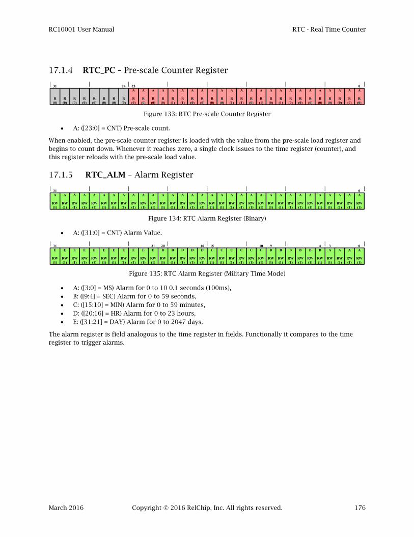
RC10001 User Manual RTC - Real Time Counter
March 2016 Copyright © 2016 RelChip, Inc. All rights reserved. 176
17.1.4 RTC_PC – Pre-scale Counter Register
Figure 133: RTC Pre-scale Counter Register
A: ([23:0] = CNT) Pre-scale count.
When enabled, the pre-scale counter register is loaded with the value from the pre-scale load register and begins to count down. Whenever it reaches zero, a single clock issues to the time register (counter), and this register reloads with the pre-scale load value.
17.1.5 RTC_ALM – Alarm Register
Figure 134: RTC Alarm Register (Binary)
A: ([31:0] = CNT) Alarm Value.
Figure 135: RTC Alarm Register (Military Time Mode)
A: ([3:0] = MS) Alarm for 0 to 10 0.1 seconds (100ms), B: ([9:4] = SEC) Alarm for 0 to 59 seconds, C: ([15:10] = MIN) Alarm for 0 to 59 minutes, D: ([20:16] = HR) Alarm for 0 to 23 hours, E: ([31:21] = DAY) Alarm for 0 to 2047 days.
The alarm register is field analogous to the time register in fields. Functionally it compares to the time register to trigger alarms.
R(0)
R(0)
R(0)
R(0)
R(0)
31
R(0)
R(0)
24
R(0)
A
R(1)
A
R(0)
A
R(1)
A
R(0)
A
R(0)
A
R(0)
A
R(0)
A
R(0)
A
R(0)
A
R(0)
0A
R(0)
A
R(0)
A
R(1)
A
R(1)
A
R(0)
A
R(0)
A
R(0)
A
R(0)
A
R(1)
A
R(1)
A
R(0)
A
R(0)
A
R(0)
23A
R(0)
0A
RW(1)
A
RW(1)
31A
RW(1)
A
RW(1)
A
RW(1)
A
RW(1)
A
RW(1)
A
RW(1)
A
RW(1)
A
RW(1)
A
RW(1)
A
RW(1)
A
RW(1)
A
RW(1)
A
RW(1)
A
RW(1)
A
RW(1)
A
RW(1)
A
RW(1)
A
RW(1)
A
RW(1)
A
RW(1)
A
RW(1)
A
RW(1)
A
RW(1)
A
RW(1)
A
RW(1)
A
RW(1)
A
RW(1)
A
RW(1)
A
RW(1)
A
RW(1)
0A
RW(1)
A
RW(1)
A
RW(1)
3A
RW(1)
4B
RW(1)
9B
RW(1)
C
RW(1)
15C
RW(1)
16D
RW(1)
20D
RW(1)
21E
RW(1)
E
RW(1)
31E
RW(1)
D
RW(1)
10C
RW(1)
B
RW(1)
D
RW(1)
D
RW(1)
E
RW(1)
E
RW(1)
E
RW(1)
E
RW(1)
E
RW(1)
E
RW(1)
E
RW(1)
E
RW(1)
C
RW(1)
C
RW(1)
C
RW(1)
B
RW(1)
B
RW(1)
B
RW(1)

RC10001 User Manual RTC - Real Time Counter
March 2016 Copyright © 2016 RelChip, Inc. All rights reserved. 177
17.1.6 RTC_IE - Interrupt Enable Register
Figure 136: RTC Interrupt Enable Register
A: ([0] = IE) Interrupt Enable.
Only one interrupt is output from the real time clock, the alarm.
17.1.7 RTC_RIS - Raw Interrupt Status Register
Figure 137: RTC Raw Interrupt Status Register
A: ([0] = RIS) Raw Interrupt Status.
Independent of the interrupt enable, the raw interrupt status register will report alarms. The alarm signal asserts a full minimum time increment (determined by the pre-scale register).
17.1.8 RTC_MIS - Masked Interrupt Status Register
Figure 138: RTC Masked Interrupt Status Register
A: ([0] = MIS) Masked Interrupt Status.
The masked interrupt register represents the logical AND of the interrupt enable and the UART_RIS register.
17.1.9 RTC_ICR Interrupt Clear Register
Figure 139: RTC Interrupt Clear Register
A: ([0] = ICR) Interrupt Clear Register.
Writing a one to ICR will clear the interrupt. This bit auto-resets on the next cycle.
0A
RW(0)
R(0)
31
R(0)
R(0)
R(0)
R(0)
R(0)
R(0)
R(0)
R(0)
R(0)
R(0)
R(0)
R(0)
R(0)
R(0)
R(0)
R(0)
R(0)
R(0)
R(0)
R(0)
R(0)
R(0)
R(0)
R(0)
R(0)
R(0)
R(0)
R(0)
R(0)
1
R(0)
R(0)
R(0)
R(0)
R(0)
R(0)
31
R(0)
R(0)
0A
R(0)
R(0)
R(0)
R(0)
R(0)
R(0)
R(0)
R(0)
R(0)
R(0)
R(0)
R(0)
R(0)
R(0)
R(0)
R(0)
R(0)
R(0)
R(0)
R(0)
R(0)
R(0)
R(0)
R(0)
1
R(0)
R(0)
R(0)
R(0)
R(0)
R(0)
31
R(0)
R(0)
0A
R(0)
R(0)
R(0)
R(0)
R(0)
R(0)
R(0)
R(0)
R(0)
R(0)
R(0)
R(0)
R(0)
R(0)
R(0)
R(0)
R(0)
R(0)
R(0)
R(0)
R(0)
R(0)
R(0)
R(0)
1
R(0)
31 0A
WP
1

RC10001 User Manual WDT - Watchdog Timer
March 2016 Copyright © 2016 RelChip, Inc. All rights reserved. 178
18 WDT - WATCHDOG TIMER
The watchdog timer is a twenty-four bit unsigned integer counter (countdown). Upon an enable and feed, the counter loads and begins to count down. Upon reaching zero, the RC10001 will be reset or an interrupt will be generated. Reset and interrupt selection is configured. This is a failsafe counter. Once enabled, only reset disables it. The code should provide periodic feeds.
The SYSCON_AHBCLKCTRL - Clock Enable Register enables the clock. Upon reset, the clock is disabled.
18.1 REGISTERS
Table 47: Watchdog Timer Register Map
Register Access Address(1) Description
MOD RW 0x4000_4000 Mode
TC RW 0x4000_4004 Time Out
FEED WO 0x4000_4008 Feed Sequence
TV RO 0x4000_400C Timer Value
- ? 0x4000_4010 to
0x4000_7FFF Reserved
18.1.1 WDT_MOD – Mode Register
Figure 140: WDT Mode Register
A: ([0] = WDEN) Watchdog enable. Write to a one to enable the timer. A feed starts the watchdog timer. The watch dog cannot be disabled except by a reset,
B: ([1] = WDRESET) Watchdog reset enable. When written to a one, a time out of the watchdog timer will reset the RC10001. Writing a zero has no effect. The bit resets to a zero,
C: ([2] = WDTOF) Watchdog timeout flag. When the watchdog timer completes, this flag is set. The flag is cleared by writing a zero. Writing a one has no effect,
D: ([3] = WDINT) Watch dog interrupt flag. This is a read only bit that reports the current state of the watchdog interrupt. A reset will clear this flag.
0A
RW1(0)
1B
RW1(0)
2C
RW0(0)
3D
R(0)
31
R(0)
R(0)
R(0)
R(0)
R(0)
R(0)
R(0)
R(0)
R(0)
R(0)
R(0)
R(0)
R(0)
R(0)
R(0)
R(0)
R(0)
R(0)
R(0)
R(0)
R(0)
R(0)
R(0)
R(0)
R(0)
R(0)
R(0)
4
R(0)

RC10001 User Manual WDT - Watchdog Timer
March 2016 Copyright © 2016 RelChip, Inc. All rights reserved. 179
18.1.2 WDT_TC – Time Out Register
Figure 141: WDT Timer Constant Register
A: ([23:0] = COUNT) Count to load for the next watchdog count.
The timer constant is a read/write twenty-four bit unsigned integer that is loaded in the counter (WDT_TV). The minimum allowed value is 0x00_00FF. Attempting to write smaller values will set the register to 0x00_00FF. On reset, 0x00_00FF is set.
18.1.3 WDT_FEED – Feed Sequence Register
Figure 142: WDT Feed Register
A: ([7:0] = FEED) Feed value.
To either start or reset the watchdog timer, a series of two numbers in sequence need to be loaded into the FEED register. This prevents false starts of the watchdog timer by “stray” user code. A 0x0F followed by a 0xF0 trigger proper operation. When fed with the sequence, the TC value is stored in the TV register. The TV register will then begin to count down.
The feed sequence is 0x0F/0xF0. This sequence is written to the feed register, resetting the counter.
To insure that the watchdog timer does not reset the part while servicing interrupts, disable interrupts during the feed sequence.
18.1.4 WDT_TV – Timer Value Register
Figure 143: WDT Timer Value Register
A: ([23:0] = COUNT) Current watchdog count.
This read-only twenty-four bit unsigned integer is the current value of the watchdog timer. It is loaded from the WDT_TC register by a feed sequence.
0A
RW(1)
R(0)
31
R(0)
R(0)
R(0)
R(0)
R(0)
R(0)
24
R(0)
A
RW(1)
A
RW(1)
A
RW(1)
A
RW(1)
A
RW(1)
A
RW(1)
A
RW(1)
A
RW(0)
A
RW(0)
A
RW(0)
A
RW(0)
A
RW(0)
A
RW(0)
A
RW(0)
A
RW(0)
A
RW(0)
A
RW(0)
A
RW(0)
A
RW(0)
A
RW(0)
A
RW(0)
A
RW(0)
23A
RW(0)
31 0A
W
8A
W
A
W
A
W
A
W
A
W
A
W
7A
W
R(0)
R(0)
R(0)
R(0)
R(0)
31
R(0)
R(0)
0A
R(X)
24
R(0)
A
R(X)
A
R(X)
A
R(X)
A
R(X)
A
R(X)
A
R(X)
A
R(X)
A
R(X)
A
R(X)
A
R(X)
A
R(X)
A
R(X)
A
R(X)
A
R(X)
A
R(X)
A
R(X)
A
R(X)
A
R(X)
A
R(X)
A
R(X)
A
R(X)
A
R(X)
23A
R(X)
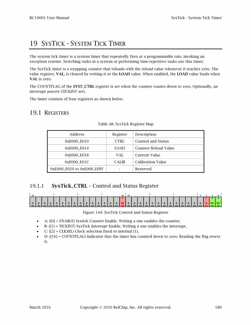
RC10001 User Manual SysTick - System Tick Timer
March 2016 Copyright © 2016 RelChip, Inc. All rights reserved. 180
19 SYSTICK - SYSTEM TICK TIMER
The system tick timer is a system timer that repeatedly fires at a programmable rate, invoking an exception routine. Switching tasks in a system or performing time-repetitive tasks use this timer.
The SysTick timer is a wrapping counter that reloads with the reload value whenever it reaches zero. The value register, VAL, is cleared by writing it or the LOAD value. When enabled, the LOAD value loads when VAL is zero.
The COUNTFLAG of the SYST_CTRL register is set when the counter counts down to zero. Optionally, an interrupt asserts (TICKINT set).
The timer consists of four registers as shown below.
19.1 REGISTERS
Table 48: SysTick Register Map
Address Register Description
0xE000_E010 CTRL Control and Status
0xE000_E014 LOAD Counter Reload Value
0xE000_E018 VAL Current Value
0xE000_E01C CALIB Calibration Value
0xE000_E020 to 0xE000_E0FF - Reserved
19.1.1 SysTick_CTRL – Control and Status Register
Figure 144: SysTick Control and Status Register
A: ([0] = ENABLE) Systick Counter Enable. Writing a one enables the counter, B: ([1] = TICKINT) SysTick Interrupt Enable. Writing a one enables the interrupt, C: ([2] = CLKSEL) Clock selection fixed to internal (1), D: ([16] = COUNTFLAG) Indicator that the timer has counted down to zero. Reading the flag resets
it.
0A
RW(0)
1B
RW(0)
2C
R(1)
31
R(0)
R(0)
R(0)
R(0)
R(0)
R(0)
R(0)
R(0)
R(0)
R(0)
R(0)
R(0)
R(0)
R(0)
R(0)
15
R(0)
R(0)
R(0)
R(0)
R(0)
R(0)
R(0)
R(0)
R(0)
R(0)
R(0)
R(0)
3
R(0)
16C
R0(0)
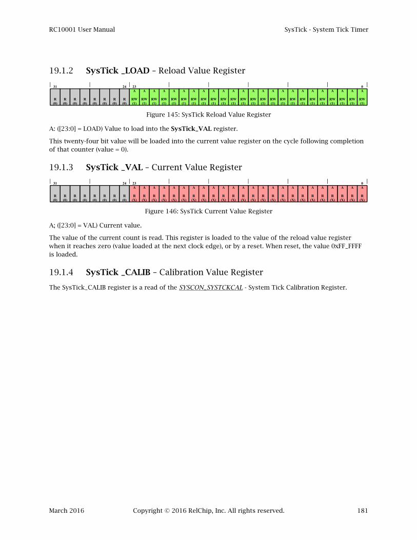
RC10001 User Manual SysTick - System Tick Timer
March 2016 Copyright © 2016 RelChip, Inc. All rights reserved. 181
19.1.2 SysTick _LOAD – Reload Value Register
Figure 145: SysTick Reload Value Register
A: ([23:0] = LOAD) Value to load into the SysTick_VAL register.
This twenty-four bit value will be loaded into the current value register on the cycle following completion of that counter (value = 0).
19.1.3 SysTick _VAL – Current Value Register
Figure 146: SysTick Current Value Register
A; ([23:0] = VAL) Current value.
The value of the current count is read. This register is loaded to the value of the reload value register when it reaches zero (value loaded at the next clock edge), or by a reset. When reset, the value 0xFF_FFFF is loaded.
19.1.4 SysTick _CALIB – Calibration Value Register
The SysTick_CALIB register is a read of the SYSCON_SYSTCKCAL - System Tick Calibration Register.
0A
RW(1)
R(0)
31
R(0)
R(0)
R(0)
R(0)
R(0)
R(0)
24
R(0)
A
RW(1)
A
RW(1)
A
RW(1)
A
RW(1)
A
RW(1)
A
RW(1)
A
RW(1)
A
RW(1)
A
RW(1)
A
RW(1)
A
RW(1)
A
RW(1)
A
RW(1)
A
RW(1)
A
RW(1)
A
RW(1)
A
RW(1)
A
RW(1)
A
RW(1)
A
RW(1)
A
RW(1)
A
RW(1)
23A
RW(1)
R(0)
R(0)
R(0)
R(0)
R(0)
31
R(0)
R(0)
0A
R(X)
24
R(0)
A
R(X)
A
R(X)
A
R(X)
A
R(X)
A
R(X)
A
R(X)
A
R(X)
A
R(X)
A
R(X)
A
R(X)
A
R(X)
A
R(X)
A
R(X)
A
R(X)
A
R(X)
A
R(X)
A
R(X)
A
R(X)
A
R(X)
A
R(X)
A
R(X)
A
R(X)
23A
R(X)
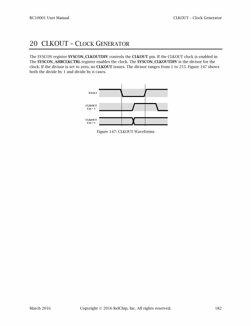
RC10001 User Manual CLKOUT – Clock Generator
March 2016 Copyright © 2016 RelChip, Inc. All rights reserved. 182
20 CLKOUT – CLOCK GENERATOR
The SYSCON register SYSCON_CLKOUTDIV controls the CLKOUT pin. If the CLKOUT clock is enabled in The SYSCON_AHBCLKCTRL register enables the clock. The SYSCON_CLKOUTDIV is the divisor for the clock. If the divisor is set to zero, no CLKOUT issues. The divisor ranges from 1 to 255. Figure 147 shows both the divide by 1 and divide by n cases.
Figure 147: CLKOUT Waveforms
XTAL1
CLKOUTCnt = 1
CLKOUTCnt > 1

RC10001 User Manual Serial Wire Debug
March 2016 Copyright © 2016 RelChip, Inc. All rights reserved. 183
21 SERIAL WIRE DEBUG
A serial wire debug interface on the RC10001 provides access to memory and registers, program control, and programmable breakpoints. The ARM architecture includes debug access through a debug port (DP) and access port (AP) as shown in Figure 148. This interface can also boot the RC10001.
Conceptually, the host debugger issues a command to the debug port. The RC10001 acknowledges this command. Then a data cycle (either to or from the host) is executed. The debug port, see the Debug Port (DP) section, processes the command. All cycle times are synchronous to the SWCLK signal from the host. The SWCLK signal clocks data asynchronous to the crystal clock, XTAL1. SWCLK cannot exceed the crystal frequency.
The access port, see the Access Port (AP) section, communicates between the debug port and the microcontroller resources. The access port reads and writes internal memory, general-purpose registers, and debug registers.
The debug port converts serial data to parallel. All serial data transmissions are thirty-two bit plus parity. All header transactions are 7 bits plus a parking bit and turnaround cycle (Figure 149 and Figure 150). Acknowledges, representing either good or bad transmissions are three bit, and a single bit time turns around the serial wire interface. The sequence is described in the Protocol section.
Figure 148: Debug Architecture
21.1 SERIAL WIRE DEBUG RESET
Transmitting fifty or more ones to the microcontroller on SWDIO resets the debug unit. The first access to the debugger must be preceded by a reset. A part reset does not reset the debug unit. This reset does not reset the entire microcontroller, only the debug unit. Note: This reset does not reset the sticky error bits. The DP_ABORT register resets the sticky bits in the debugger.
AP
Port
DP
Port
Special
Registers
AHB
Bus
Serial
Wire
Debug
Interface
ABORT
CTRL/STATIDCODE
WCR
SELECT
RESEND
RDBUFF
TAR
DRW
CSW
BASE
IDR
CFG BD1
BD2
BD0
BD3
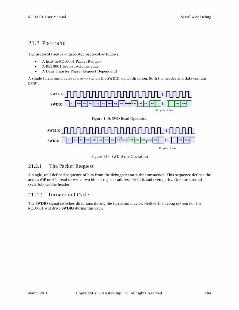
RC10001 User Manual Serial Wire Debug
March 2016 Copyright © 2016 RelChip, Inc. All rights reserved. 184
21.2 PROTOCOL
The protocol used is a three-step protocol as follows:
A host-to-RC10001 Packet Request A RC10001-to-host Acknowledge A Data Transfer Phase (Request Dependent)
A single turnaround cycle is use to switch the SWDIO signal direction. Both the header and data contain parity.
Figure 149: SWD Read Operation
Figure 150: SWD Write Operation
21.2.1 The Packet Request
A single, well-defined sequence of bits from the debugger starts the transaction. This sequence defines the access (DP or AP), read or write, two bits of register address (A[3:2]), and even parity. One turnaround cycle follows the header.
21.2.2 Turnaround Cycle
The SWDIO signal switches directions during the turnaround cycle. Neither the debug system nor the RC10001 will drive SWDIO during this cycle.
SWCLK
SWDIO ~ ~~ ~
32 cycles of data
LSB0 MSBA[3]Start A[2]ReadPort ACK1ParkStopParity ACK0 ACK2 Parity
SWCLK
SWDIO ~ ~~ ~
32 cycles of data
LSB0 MSBA[3]Start A[2]WritePort ACK1ParkStopParity ACK0 ACK2 Parity

RC10001 User Manual Serial Wire Debug
March 2016 Copyright © 2016 RelChip, Inc. All rights reserved. 185
21.2.3 Acknowledge
Once a header and turnaround cycle are complete, the RC10001 will issue an acknowledge sequence. This consists of three bits (transmitted little endian) as shown in Table 49.
Table 49: Serial Wire Debug Acknowledge Responses
Ack[0:2] Logic Description
3b100 OK Correct Acknowledge
3b010 WAIT Wait for Internal Completion
3b001 FAULT Error
none - Protocol Error
21.2.4 Data Packet
A data packet consists of thirty-two data bits (little endian) followed by an even parity bit. The first bit transmitted is D[0]. The last bits are D[31] followed by the parity bit.
21.2.5 Host Write
A data packet consists of thirty-two data bits (little endian) followed by an even parity bit. The first bit transmitted is D[0]. The last bits are D[31] followed by the parity bit. The host write is shown in Figure 150.
Table 50: Host Responses for DP Write Transactions
A[3:2] Sticky Flag? AP Ready? ACK Description
2b00 X X OK Write ABORT Register
2b01 No Yes OK Write CTRL Register (all swd)
2b10 No Yes OK Write SELECT Register (swd_1)
2b11 No Yes OK Not Available
!(2b00) No No WAIT No Data Phase (1)
!(2b00) Yes X FAULT No Data Phase (1)
NOTES:
1. If Overrun Detection is enabled, data phase is completed.
Table 51: Host Responses for AP Write Transactions
Sticky Flag? AP Ready? ACK Description
No Yes OK Write Addressed AP Register
No No WAIT No Data Phase (1)
Yes X FAULT No Data Phase (1)
NOTES:
1. If Overrun Detection is enabled, data phase is completed.

RC10001 User Manual Serial Wire Debug
March 2016 Copyright © 2016 RelChip, Inc. All rights reserved. 186
21.2.6 Host Read
A data packet consists of thirty-two data bits (little endian) followed by an even parity bit. The first bit transmitted is D[0]. The last bits are D[31] followed by the parity bit. An example correct transaction is shown in Figure 149.
Table 52: Host Expectations from a DP Read Transaction
A[3:2] Sticky Flag? AP Ready? ACK Register and Description
2b00 X X OK IDCODE Value Read (swd_1)
2b01 X X OK STAT or WCR Value Read (swd_1)
2b10 No Yes OK RESEND: Read Most Recently Read (1)
2b11 No Yes OK RDBUFF: Read AP (2)
2b10 No No WAIT RESEND: No Data Phase (3)
2b11 No No WAIT RDBUFF: No Data Phase (3)
2b10 Yes X FAULT RESEND: No Data Phase (3)
2b11 Yes X FAULT RDBUFF: No Data Phase (3)
NOTES:
1. Resends the last value from either the most recent AP read or DP RDBUFF read. 2. Resends the most recent AP Read and sets the READOK flag in the CTRL/STAT Register to 1. 3. If Overrun Detection is enabled, the data phase is completed.
Table 53: Host Expectations from an AP Read Transaction
Sticky Flag? AP Ready? ACK Description
No Yes OK Read Addressed AP Register
No No WAIT No Data Phase (1)
Yes X FAULT No Data Phase (1)
NOTES:
1. If Overrun Detection is enabled, data phase is completed.
21.2.7 AP Posted Reads
AP reads post. With an AP read request, the AP read occurs with the result “staged” at the DP. A following DP RDBUFF read will obtain the results. However, if you are making a series of AP reads, these can be used to obtain the results (only the last read must be to the DP RDBUFF) as follows:
AP read access[0] -> data is unpredictable AP read access[1] -> access[0] is returned ... AP read access[n] -> access[n-1] is returned DP RDBUFF access -> access[n] is returned

RC10001 User Manual Serial Wire Debug
March 2016 Copyright © 2016 RelChip, Inc. All rights reserved. 187
21.2.8 READOK and RESEND
The CTRL/STAT register READOK flag updates on every AP read access and every RDBUFF read request. It represents the header acknowledge returns, or specifically is set on an “OK” acknowledge, or cleared on any other acknowledge.
If the host debugger receives a bad acknowledge from an appropriate read request, it can check for correct completion of the read. If the READOK flag is set, the host can use a RESEND request to get the correct data. If the flag is not set, the host must reissue the original read request.

RC10001 User Manual Serial Wire Debug
March 2016 Copyright © 2016 RelChip, Inc. All rights reserved. 188
21.2.9 WAIT Status
A WAIT Acknowledge responses when the SWD is unable to process a request. If the SWCLK is much lower than the frequency of system, this should never occur. The internal SWD unit is still processing the previous command. The host must back off and resend the command.
Note that reading the IDCODE, reading the CTRL/STAT register, or writing the ABORT register can only assert an OK acknowledge.
A transaction acknowledged with a WAIT aborts the data phase unless the overrun detection is enabled. Figure 151 and Figure 152 show both possibilities. During a read attempt, the host debugger will ignore the data and the RC10001 will not drive it. During a write attempt, the RC10001 will ignore the data. In either case, the data is only transmitted when overrun detection is enabled.
Figure 151: SWD DP RESEND Read with WAIT Acknowledge
Figure 152: SWD DP SELECT Write with WAIT Acknowledge
SWCLK
SWDIO ~ ~~ ~
32 cycles of data
LSB0 MSBA[3]Start A[2]ReadDP ACK1ParkStopParity ACK0 ACK2 Parity
WAIT Acknowledge
b) with Overrun Detection Enabled
SWCLK
SWDIO 0 A[3]Start A[2]ReadDP ACK1ParkStopParity ACK0 ACK2
WAIT Acknowledge
a) with Overrun Detection Disabled
SWCLK
SWDIO ~ ~~ ~
32 cycles of data
LSB0 MSBA[3]Start A[2]WriteDP ACK1ParkStopParity ACK0 ACK2 Parity
WAIT Acknowledge
b) with Overrun Detection Enabled
SWCLK
SWDIO 0 A[3]Start A[2]WriteDP ACK1ParkStopParity ACK0 ACK2
WAIT Acknowledge
a) with Overrun Detection Disabled
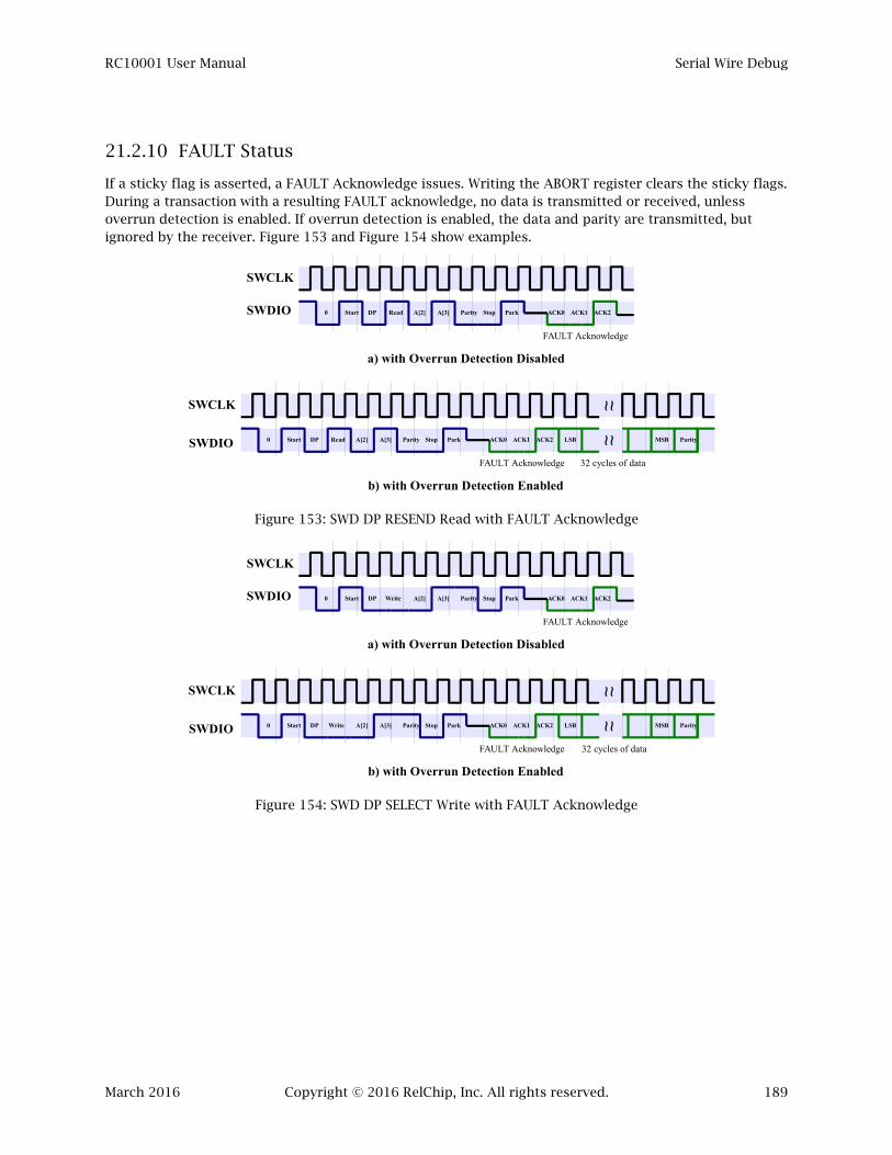
RC10001 User Manual Serial Wire Debug
March 2016 Copyright © 2016 RelChip, Inc. All rights reserved. 189
21.2.10 FAULT Status
If a sticky flag is asserted, a FAULT Acknowledge issues. Writing the ABORT register clears the sticky flags. During a transaction with a resulting FAULT acknowledge, no data is transmitted or received, unless overrun detection is enabled. If overrun detection is enabled, the data and parity are transmitted, but ignored by the receiver. Figure 153 and Figure 154 show examples.
Figure 153: SWD DP RESEND Read with FAULT Acknowledge
Figure 154: SWD DP SELECT Write with FAULT Acknowledge
SWCLK
SWDIO ~ ~~ ~
32 cycles of data
LSB0 MSBA[3]Start A[2]ReadDP ACK1ParkStopParity ACK0 ACK2 Parity
FAULT Acknowledge
b) with Overrun Detection Enabled
SWCLK
SWDIO 0 A[3]Start A[2]ReadDP ACK1ParkStopParity ACK0 ACK2
FAULT Acknowledge
a) with Overrun Detection Disabled
SWCLK
SWDIO ~ ~~ ~
32 cycles of data
LSB0 MSBA[3]Start A[2]WriteDP ACK1ParkStopParity ACK0 ACK2 Parity
FAULT Acknowledge
b) with Overrun Detection Enabled
SWCLK
SWDIO 0 A[3]Start A[2]WriteDP ACK1ParkStopParity ACK0 ACK2
FAULT Acknowledge
a) with Overrun Detection Disabled
RC10001 User Manual Serial Wire Debug
March 2016 Copyright © 2016 RelChip, Inc. All rights reserved. 190
21.2.11 Protocol Errors
A protocol error occurs whenever there is an error in the header. The simple RC10001 response is “no response.” The host detects no valid acknowledge, and tries again. If continued tries yield no results, the host should read the IDCODE. If this fails, the host should reset the debug interface and try again.
21.2.12 Write Data Parity Errors
If the write data fails parity in the RC10001, the write is aborted and the WDATAERR bit in the CTRL/STAT register is set. WDATA fails parity check. A data packet consists of thirty-two data bits (little endian) followed by an even parity bit. The first bit transmitted is D[0]. The last bits are D[31] followed by the parity bit.
21.2.13 Sticky Flags
A sticky flag retains the set value (one) until explicitly cleared. The sticky flags are WDATAERR, STICKYERR, and STICKORUN located in the DP_STAT register. Parity errors, framing errors, or a discarded AP write issue WDATAERR. An AP transaction error asserts the STICKYERR bit. The STICKORUN bit is set whenever there is an overrun, subject to enabling by the ORUNDETECT bit of the DP_CTRL register.
Reception errors at the DP level trigger WDATAERR. If a parity bit indicates an error either in the header, or in the data, the bit is set. The WDERRCLR bit (DP_ABORT register) clears the WDATAERR bit.
AP read and write errors trigger STICKYERR. One example of this would be accessing the AP unit while the power is down (CDBGPWRUPACK in the DP_STAT register equals 0). Writing the STKERRCLR bit clears the STICKYERR bit.
The STICKORUN is triggered by any response (acknowledge) other than OK. The ORUNDETECT bit of the DP_CTRL register enables this mode. Writing the ORUNERRCLR bit clears the STICKORUN bit.
When first initializing the part, the user should 1. Read the DP_IDCODE register, 2. Write the DP_CTRL register to enable the debugger, 3. Write the DP_SELECT register for the bank, and 4. Write the DP_ABORT register to clear the sticky bits.

RC10001 User Manual Serial Wire Debug
March 2016 Copyright © 2016 RelChip, Inc. All rights reserved. 191
21.3 DEBUG PORT (DP)
The debug port is the interface between the external serial wire channel and the access port. The debug port responds to commands from the host debugger, issues acknowledges (including errors), and performs serial/parallel conversion of the communications.
Memory operations do not access the DP registers. Only the debug port can access them.
Table 54: DP Register Map
A[3:2] CTRLSEL Register Description
2b00 X IDCODE Identification Code
2b00 X ABORT Abort and Sticky Flag Clear
2b01 0 CTRL/STAT Control and Status
2b01 1 WCR Wire Control
2b10 X RDBUFF Read Buffer
2b10 X SELECT AP Select
2b11 X RESEND Resend
21.3.1 DP_IDCODE - Identification Code Register
Figure 155: DP Identification Code Register
A: ([11:0] = DESIGNER) ARM Designer (0x477) B: ([27:12] = PARTNO) ARM DAP Part Number (0xBB11) C: ([31:28] = VER) Version Number (0x0)
This register identifies the DP Design and JEDEC code for the RC10001.
0A
R(1)
A
R(1)
A
R(1)
A
R(0)
A
R(1)
A
R(1)
A
R(1)
A
R(0)
A
R(0)
A
R(0)
A
R(1)
11A
R(0)
12B
R(1)
B
R(0)
B
R(0)
B
R(0)
B
R(1)
B
R(0)
B
R(0)
B
R(0)
B
R(1)
B
R(1)
B
R(0)
B
R(1)
B
R(1)
B
R(1)
B
R(0)
27B
R(1)
28C
R(0)
C
R(0)
C
R(0)
31C
R(0)

RC10001 User Manual Serial Wire Debug
March 2016 Copyright © 2016 RelChip, Inc. All rights reserved. 192
21.3.2 DP_ABORT - Abort Register
Figure 156: DP Abort Register
A: ([0] = DAPABORT) Generates a DAP abort to keep from locking up in an infinite wait state, B: ([2] = STKERRCLR) Writing a one will clear the STICKYERR bit in the DP_STAT register, C: ([3] = WDERRCLR) Writing a one will clear the WDATAERR bit in the DP_STAT register, D: ([4] = ORUNERRCLR) Writing a one will clear the STICKORUN error bit in the DP_STAT register.
21.3.3 DP_CTRL/DP_STAT - Control and Status Register
Figure 157: DP Control and Status Register
A: ([0] = ORUNDETECT) Written to one to enable overrun detection. The STICKORUN bit is enabled by this,
B: ([1] = STICKORUN) Set to one when enabled by ORUNDETECT and any response other than OK was sent,
C: ([5] = STICKYERR) Set to one by read and write errors, D: ([6] = READOK) Set to one when the last read of the DAP acknowledged an OK, E: ([7] = WDATAERR) Sticky Error Flag for DP header and data parity errors, F: ([28] = CDBGPWRUPREQ) Request Power for DAP. Writing this bit to one requests power for the
DAP. When the acknowledge goes to one, the power is applied. Writing this bit to zero requests a power down of the DAP. When the acknowledge goes low, the power is off,
G: ([29] = CDBGPWRUPACK) Acknowledge for DAP Power Up Request. This will be set (1) when power is available in the DAP. This will be low when there is no DAP power.
Writing CDBGPWRUPREQ high powers up the debug system. When the power up sequence is finished, a read will show CDBGPWRUPACK set. This signal low indicates the no debugger power. The same sequence occurs on a power down operation. First, set the CDBGPWRUPREQ low, and when complete, the CDBGPWRUPACK goes low.
21.3.4 DP_WCR - Wire Control Register
This read only register replies with ARM® standard codes for a synchronous SWD and using a single turnaround cycle. The returned value is 0x0000_0040.
21.3.5 DP_RDBUFF - Read Buffer Register
Figure 158: DP Read Buffer Register
A: ([31:0] = VALUE) Value read from the AP
31 0A
WP
5 12B
WP
4D
WP
3C
WP
0A
RW(0)
29G
R(1)
31
R(0)
30
R(0)
27
R(0)
R(0)
R(0)
R(0)
R(0)
R(0)
R(0)
R(0)
R(0)
R(0)
R(0)
R(0)
R(0)
R(0)
R(0)
R(0)
R(0)
R(0)
8
R(0)
4
R(0)
R(0)
1B
R(0)
2
R(0)
5C
R(0)
6D
R(0)
7E
R(0)
R(0)
28F
W
0A
R(X)
A
R(X)
A
R(X)
A
R(X)
A
R(X)
A
R(X)
A
R(X)
A
R(X)
A
R(X)
A
R(X)
A
R(X)
A
R(X)
A
R(X)
A
R(X)
A
R(X)
A
R(X)
A
R(X)
A
R(X)
A
R(X)
A
R(X)
A
R(X)
A
R(X)
A
R(X)
A
R(X)
A
R(X)
A
R(X)
A
R(X)
A
R(X)
A
R(X)
A
R(X)
A
R(X)
31A
R(X)

RC10001 User Manual Serial Wire Debug
March 2016 Copyright © 2016 RelChip, Inc. All rights reserved. 193
The read buffer register is a thirty-two bit register that, when read returns the value of the last AP read operation. If read a second time, the data is invalid. To read the same data again, use the DP_RESEND register.
21.3.6 DP_SELECT - AP Select Register
Figure 159: DP Select Register
A: ([0] = CTRLSEL) Control Register Select. A one enables addressing the DP_WCR, while a zero enables access of the DP_CTRL/DP_STAT register,
B: ([7:4] = APBANKSEL) AP Unit Bank Selection. Support for three banks only, 0x0, 0x1, and 0xF exists. See Access Port (AP),
C: ([31:24] = APSEL) AP Unit Selection. There is only one AP unit in the RC10001 with an select of 0x0.
21.3.7 DP_RESEND - Resend Register
Figure 160: DP Resend Register
The resend register captures the data from the most recent AP read or RDBUFF read. Multiple register reads of the resend register does not change the data.
0A
W
8 4B
W
B
W
B
W
7B
W
24C
W
C
W
C
W
C
W
C
W
C
W
C
W
31C
W
23 3 1
0A
R(X)
A
R(X)
A
R(X)
A
R(X)
A
R(X)
A
R(X)
A
R(X)
A
R(X)
A
R(X)
A
R(X)
A
R(X)
A
R(X)
A
R(X)
A
R(X)
A
R(X)
A
R(X)
A
R(X)
A
R(X)
A
R(X)
A
R(X)
A
R(X)
A
R(X)
A
R(X)
A
R(X)
A
R(X)
A
R(X)
A
R(X)
A
R(X)
A
R(X)
A
R(X)
A
R(X)
31A
R(X)
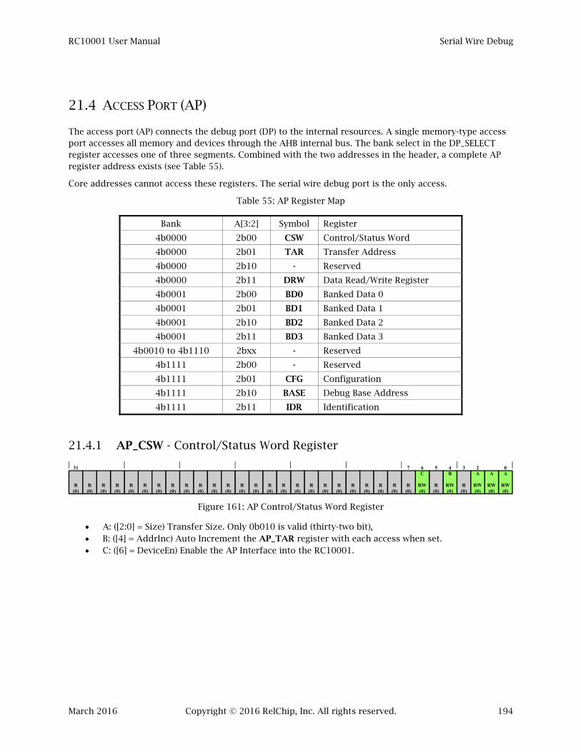
RC10001 User Manual Serial Wire Debug
March 2016 Copyright © 2016 RelChip, Inc. All rights reserved. 194
21.4 ACCESS PORT (AP)
The access port (AP) connects the debug port (DP) to the internal resources. A single memory-type access port accesses all memory and devices through the AHB internal bus. The bank select in the DP_SELECT register accesses one of three segments. Combined with the two addresses in the header, a complete AP register address exists (see Table 55).
Core addresses cannot access these registers. The serial wire debug port is the only access.
Table 55: AP Register Map
Bank A[3:2] Symbol Register
4b0000 2b00 CSW Control/Status Word
4b0000 2b01 TAR Transfer Address
4b0000 2b10 - Reserved
4b0000 2b11 DRW Data Read/Write Register
4b0001 2b00 BD0 Banked Data 0
4b0001 2b01 BD1 Banked Data 1
4b0001 2b10 BD2 Banked Data 2
4b0001 2b11 BD3 Banked Data 3
4b0010 to 4b1110 2bxx - Reserved
4b1111 2b00 - Reserved
4b1111 2b01 CFG Configuration
4b1111 2b10 BASE Debug Base Address
4b1111 2b11 IDR Identification
21.4.1 AP_CSW - Control/Status Word Register
Figure 161: AP Control/Status Word Register
A: ([2:0] = Size) Transfer Size. Only 0b010 is valid (thirty-two bit), B: ([4] = AddrInc) Auto Increment the AP_TAR register with each access when set. C: ([6] = DeviceEn) Enable the AP Interface into the RC10001.
0A
RW(0)
31
R(0)
R(0)
R(0)
R(0)
R(0)
R(0)
R(0)
R(0)
R(0)
R(0)
R(0)
R(0)
R(0)
R(0)
R(0)
R(0)
R(0)
R(0)
R(0)
3
R(0)
R(0)
A
RW(0)
2A
RW(0)
4B
RW(0)
5
R(0)
6C
RW(0)
7
R(0)
R(0)
R(0)
R(0)
R(0)
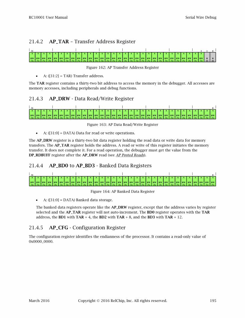
RC10001 User Manual Serial Wire Debug
March 2016 Copyright © 2016 RelChip, Inc. All rights reserved. 195
21.4.2 AP_TAR – Transfer Address Register
Figure 162: AP Transfer Address Register
A: ([31:2] = TAR) Transfer address.
The TAR register contains a thirty-two bit address to access the memory in the debugger. All accesses are memory accesses, including peripherals and debug functions.
21.4.3 AP_DRW - Data Read/Write Register
Figure 163: AP Data Read/Write Register
A: ([31:0] = DATA) Data for read or write operations.
The AP_DRW register is a thirty-two bit data register holding the read data or write data for memory transfers. The AP_TAR register holds the address. A read or write of this register initiates the memory transfer. It does not complete it. For a read operation, the debugger must get the value from the DP_RDBUFF register after the AP_DRW read (see AP Posted Reads).
21.4.4 AP_BD0 to AP_BD3 - Banked Data Registers
Figure 164: AP Banked Data Register
A: ([31:0] = DATA) Banked data storage.
The banked data registers operate like the AP_DRW register, except that the address varies by register selected and the AP_TAR register will not auto-increment. The BD0 register operates with the TAR address, the BD1 with TAR + 4, the BD2 with TAR + 8, and the BD3 with TAR + 12.
21.4.5 AP_CFG - Configuration Register
The configuration register identifies the endianness of the processor. It contains a read-only value of 0x0000_0000.
1
R(0)
2A
RW(X)
A
RW(X)
0
R(0)
A
RW(X)
A
RW(X)
A
RW(X)
A
RW(X)
A
RW(X)
A
RW(X)
A
RW(X)
A
RW(X)
A
RW(X)
A
RW(X)
A
RW(X)
A
RW(X)
A
RW(X)
A
RW(X)
A
RW(X)
A
RW(X)
A
RW(X)
A
RW(X)
A
RW(X)
A
RW(X)
A
RW(X)
A
RW(X)
A
RW(X)
A
RW(X)
A
RW(X)
A
RW(X)
A
RW(X)
31A
RW(X)
0A
RW(X)
A
RW(X)
A
RW(X)
A
RW(X)
A
RW(X)
A
RW(X)
A
RW(X)
A
RW(X)
A
RW(X)
A
RW(X)
A
RW(X)
A
RW(X)
A
RW(X)
A
RW(X)
A
RW(X)
A
RW(X)
A
RW(X)
A
RW(X)
A
RW(X)
A
RW(X)
A
RW(X)
A
RW(X)
A
RW(X)
A
RW(X)
A
RW(X)
A
RW(X)
A
RW(X)
A
RW(X)
A
RW(X)
31A
RW(X)
A
RW(X)
A
RW(X)
0A
RW(X)
A
RW(X)
A
RW(X)
A
RW(X)
A
RW(X)
A
RW(X)
A
RW(X)
A
RW(X)
A
RW(X)
A
RW(X)
A
RW(X)
A
RW(X)
A
RW(X)
A
RW(X)
A
RW(X)
A
RW(X)
A
RW(X)
A
RW(X)
A
RW(X)
A
RW(X)
A
RW(X)
A
RW(X)
A
RW(X)
A
RW(X)
A
RW(X)
A
RW(X)
A
RW(X)
A
RW(X)
A
RW(X)
31A
RW(X)
A
RW(X)
A
RW(X)
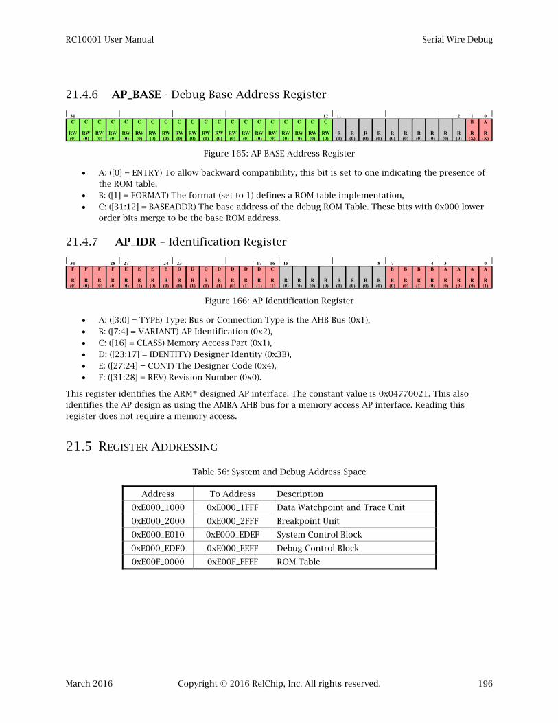
RC10001 User Manual Serial Wire Debug
March 2016 Copyright © 2016 RelChip, Inc. All rights reserved. 196
21.4.6 AP_BASE - Debug Base Address Register
Figure 165: AP BASE Address Register
A: ([0] = ENTRY) To allow backward compatibility, this bit is set to one indicating the presence of the ROM table,
B: ([1] = FORMAT) The format (set to 1) defines a ROM table implementation, C: ([31:12] = BASEADDR) The base address of the debug ROM Table. These bits with 0x000 lower
order bits merge to be the base ROM address.
21.4.7 AP_IDR – Identification Register
Figure 166: AP Identification Register
A: ([3:0] = TYPE) Type: Bus or Connection Type is the AHB Bus (0x1), B: ([7:4] = VARIANT) AP Identification (0x2), C: ([16] = CLASS) Memory Access Part (0x1), D: ([23:17] = IDENTITY) Designer Identity (0x3B), E: ([27:24] = CONT) The Designer Code (0x4), F: ([31:28] = REV) Revision Number (0x0).
This register identifies the ARM® designed AP interface. The constant value is 0x04770021. This also identifies the AP design as using the AMBA AHB bus for a memory access AP interface. Reading this register does not require a memory access.
21.5 REGISTER ADDRESSING
Table 56: System and Debug Address Space
Address To Address Description
0xE000_1000 0xE000_1FFF Data Watchpoint and Trace Unit
0xE000_2000 0xE000_2FFF Breakpoint Unit
0xE000_E010 0xE000_EDEF System Control Block
0xE000_EDF0 0xE000_EEFF Debug Control Block
0xE00F_0000 0xE00F_FFFF ROM Table
C
RW(0)
31C
RW(0)
C
RW(0)
C
RW(0)
C
RW(0)
C
RW(0)
C
RW(0)
C
RW(0)
C
RW(0)
C
RW(0)
C
RW(0)
C
RW(0)
C
RW(0)
C
RW(0)
C
RW(0)
C
RW(0)
C
RW(0)
C
RW(0)
C
RW(0)
12C
RW(0)
0A
R(X)
1B
R(X)
11
R(0)
R(0)
R(0)
R(0)
R(0)
R(0)
R(0)
R(0)
R(0)
2
R(0)
0A
R(1)
A
R(0)
A
R(0)
3A
R(0)
4B
R(0)
B
R(1)
B
R(0)
7B
R(0)
8
R(0)
R(0)
R(0)
R(0)
R(0)
R(0)
R(0)
15
R(0)
16C
R(1)
17D
R(1)
D
R(1)
D
R(0)
D
R(1)
D
R(1)
D
R(1)
23D
R(0)
24E
R(0)
E
R(0)
E
R(1)
27E
R(0)
28F
R(0)
F
R(0)
F
R(0)
31F
R(0)

RC10001 User Manual Serial Wire Debug
March 2016 Copyright © 2016 RelChip, Inc. All rights reserved. 197
21.5.1 Data Watchpoint and Trace Unit (DWT)
The Data Watchpoint and Trace Unit is an external PC sampling system to set watchpoints for data address and instruction address matches. A watchpoint event (match) results in the processor halting and entry into the debug state. The debug return address is set to next instruction. These registers are only accessible by the debug port.
The RC10001 contains one watchpoint unit. A watchpoint unit consists of a comparator register, a mask register, and the function register.
The DWT only matches on a range of addresses. The breakpoint unit matches exactly.
Program counter sampling returns the address of a “recently” executed instruction. It returns 0xffffffff if the processor is in debug state, the processor is in a state where non-invasive debug is not permitted, or the address of a recently executed instruction is not available. The use of this register is to assist profiling and delays from currently executing instructions and the PC sampling register are not deterministic.
Caveat: Instruction address matches can only occur on the first halfword (2b00) address. Only a range of addresses is support, so for fine-grained breaks, use the breakpoint unit.
Caveat: Instruction address match on a NOP yields unpredictable results.
Table 57: DWT Register Map
Address Register Description Reset
0xE000_1000 DWT_CTRL Control 0x1000_0000
0xE000_1004 to 0xE000_100B Reserved -
0xE000_101C DWT_PCSR Program Counter Sample -
0xE000_1020 DWT_COMP Comparator -
0xE000_1024 DWT_MASK Comparator Mask 0x0000_001F
0xE000_1028 DWT_FUNTION Comparator Function 0x0000_0000
0xE000_102C to 0xE000_1FFF Reserved -

RC10001 User Manual Serial Wire Debug
March 2016 Copyright © 2016 RelChip, Inc. All rights reserved. 198
21.5.1.1 DWT_CTRL - Control Register
Figure 167: DWT Control Register
A: ([31:28] = NUMCOMP) Number of Comparators (0x1)
21.5.1.2 DWT_PCSR - Program Counter Sample Register
Figure 168: DWT Program Counter Sample Register
A: ([31:0] = SAMP) Program counter sample register (near the actual location).
The thirty-two bit DWT_PCSR is the sampled value of the program counter.
21.5.1.3 DWT_COMP - Comparator Register
Figure 169: DWT Compare Register
A: ([31:0] = COMP) Compare value.
The thirty-two bit DWT_COMP register stores the address to match. The function register determines the meaning of the match.
21.5.1.4 DWT_MASK - Comparator Mask Register
Figure 170: DWT Comparator Mask Register
A: ([4:0] = MASK) Number of addresses to use.
This register selects the bit range (number of address bits) to be compared. Writing all ones to this register, determines the maximum mask size supported.
28A
R(1)
A
R(0)
A
R(0)
31A
R(0)
27
R(0)
R(0)
R(0)
R(0)
R(0)
R(0)
R(0)
R(0)
R(0)
R(0)
R(0)
R(0)
R(0)
R(0)
R(0)
R(0)
R(0)
R(0)
R(0)
R(0)
R(0)
R(0)
R(0)
R(0)
R(0)
R(0)
R(0)
0
R(0)
0A
R(X)
A
R(X)
A
R(X)
A
R(X)
A
R(X)
A
R(X)
A
R(X)
A
R(X)
A
R(X)
A
R(X)
A
R(X)
A
R(X)
A
R(X)
A
R(X)
A
R(X)
A
R(X)
A
R(X)
A
R(X)
A
R(X)
A
R(X)
A
R(X)
A
R(X)
A
R(X)
A
R(X)
A
R(X)
A
R(X)
A
R(X)
A
R(X)
A
R(X)
A
R(X)
A
R(X)
31A
R(X)
A
RW(X)
31A
RW(X)
A
RW(X)
A
RW(X)
A
RW(X)
A
RW(X)
A
RW(X)
A
RW(X)
A
RW(X)
A
RW(X)
A
RW(X)
A
RW(X)
A
RW(X)
A
RW(X)
A
RW(X)
A
RW(X)
A
RW(X)
A
RW(X)
A
RW(X)
A
RW(X)
A
RW(X)
A
RW(X)
A
RW(X)
A
RW(X)
A
RW(X)
A
RW(X)
A
RW(X)
A
RW(X)
A
RW(X)
A
RW(X)
A
RW(X)
0A
RW(X)
4A
RW(X)
A
RW(X)
A
RW(X)
A
RW(X)
0A
RW(X)
5
R(0)
R(0)
R(0)
R(0)
R(0)
R(0)
R(0)
R(0)
R(0)
R(0)
R(0)
R(0)
R(0)
R(0)
R(0)
R(0)
R(0)
R(0)
R(0)
R(0)
R(0)
R(0)
R(0)
R(0)
R(0)
R(0)
31
R(0)

RC10001 User Manual Serial Wire Debug
March 2016 Copyright © 2016 RelChip, Inc. All rights reserved. 199
21.5.1.5 DWT_FUNCTION - Comparator Function Register
Figure 171: DWT Comparator Function Register
A: ([3:0]=FUNCTION) Defines the compare action to take as shown in Table 58, B: ([23] = MATCHED) Indicates the comparator has matched since the last register read.
Instruction and data address matching is selected with the function fields. The fields define the triggered event.
Table 58: Watchpoint Comparator Functions
DWT_FUNCTION Input Access On a Match
4b0000 - RW Disabled
4b0001 - - Reserved
4b0010 - - Reserved
4b0011 - - Reserved
4b0100 IAddr1 - PC Watchpoint Event
4b0101 DAddr2 RO Watchpoint Event
4b0110 DAddr2 WO Watchpoint Event
4b0111 DAddr2 RW Watchpoint Event
4b1XXX - - Reserved
Notes:
1. Instruction Address. 2. Data Address.
3A
RW(X)
A
RW(X)
A
RW(X)
0A
RW(X)
R(0)
R(0)
R(0)
R(0)
R(0)
R(0)
R(0)
R(0)
R(0)
R(0)
R(0)
R(0)
R(0)
R(0)
R(0)
R(0)
R(0)
22
R(0)
24
R(0)
R(0)
R(0)
R(0)
R(0)
R(0)
R(0)
31
R(0)
4
R(0)
23B
R(0)
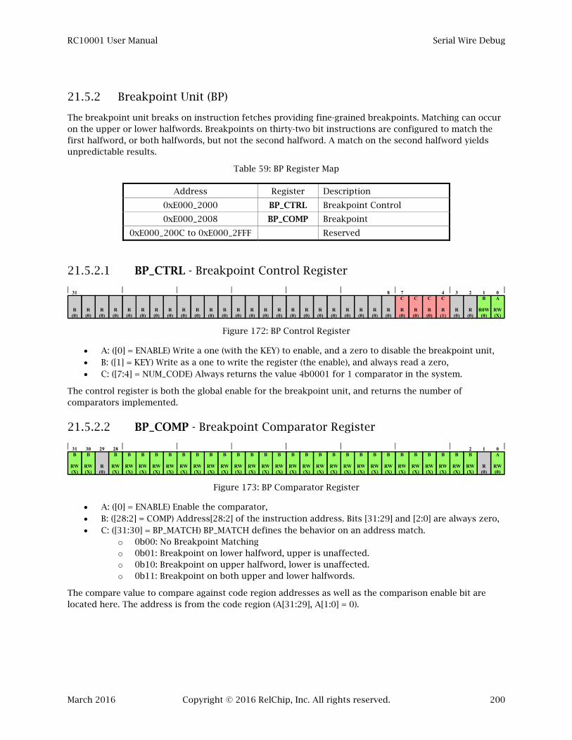
RC10001 User Manual Serial Wire Debug
March 2016 Copyright © 2016 RelChip, Inc. All rights reserved. 200
21.5.2 Breakpoint Unit (BP)
The breakpoint unit breaks on instruction fetches providing fine-grained breakpoints. Matching can occur on the upper or lower halfwords. Breakpoints on thirty-two bit instructions are configured to match the first halfword, or both halfwords, but not the second halfword. A match on the second halfword yields unpredictable results.
Table 59: BP Register Map
Address Register Description
0xE000_2000 BP_CTRL Breakpoint Control
0xE000_2008 BP_COMP Breakpoint
0xE000_200C to 0xE000_2FFF Reserved
21.5.2.1 BP_CTRL - Breakpoint Control Register
Figure 172: BP Control Register
A: ([0] = ENABLE) Write a one (with the KEY) to enable, and a zero to disable the breakpoint unit, B: ([1] = KEY) Write as a one to write the register (the enable), and always read a zero, C: ([7:4] = NUM_CODE) Always returns the value 4b0001 for 1 comparator in the system.
The control register is both the global enable for the breakpoint unit, and returns the number of comparators implemented.
21.5.2.2 BP_COMP - Breakpoint Comparator Register
Figure 173: BP Comparator Register
A: ([0] = ENABLE) Enable the comparator, B: ([28:2] = COMP) Address[28:2] of the instruction address. Bits [31:29] and [2:0] are always zero, C: ([31:30] = BP_MATCH) BP_MATCH defines the behavior on an address match.
o 0b00: No Breakpoint Matching o 0b01: Breakpoint on lower halfword, upper is unaffected. o 0b10: Breakpoint on upper halfword, lower is unaffected. o 0b11: Breakpoint on both upper and lower halfwords.
The compare value to compare against code region addresses as well as the comparison enable bit are located here. The address is from the code region (A[31:29], A[1:0] = 0).
0A
RW(X)
3
R(0)
8
R(0)
R(0)
R(0)
R(0)
R(0)
R(0)
R(0)
R(0)
R(0)
R(0)
R(0)
R(0)
R(0)
R(0)
R(0)
R(0)
R(0)
R(0)
R(0)
R(0)
R(0)
R(0)
31
R(0)
2
R(0)
7C
R(0)
1B
R0W(0)
C
R(0)
C
R(0)
4C
R(1)
R(0)
0A
RW(0)
29
R(0)
1
R(0)
2B
RW(X)
B
RW(X)
B
RW(X)
B
RW(X)
B
RW(X)
B
RW(X)
B
RW(X)
B
RW(X)
B
RW(X)
B
RW(X)
B
RW(X)
B
RW(X)
B
RW(X)
B
RW(X)
B
RW(X)
B
RW(X)
B
RW(X)
B
RW(X)
B
RW(X)
B
RW(X)
B
RW(X)
B
RW(X)
B
RW(X)
B
RW(X)
B
RW(X)
B
RW(X)
28B
RW(X)
30B
RW(X)
31B
RW(X)
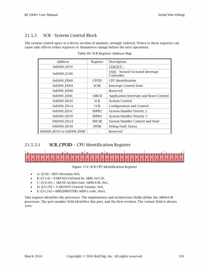
RC10001 User Manual Serial Wire Debug
March 2016 Copyright © 2016 RelChip, Inc. All rights reserved. 201
21.5.3 SCB - System Control Block
The system control space is a device section of memory, strongly ordered. Writes to these registers can cause side effects (other registers or themselves change before the next operation).
Table 60: SCB Register Address Map
Address Register Description
0xE000_E010 CLKOUT –
0xE000_E100 NVIC - Nested Vectored Interrupt Controller
0xE000_ED00 CPUID CPU Identification
0xE000_ED04 ICSR Interrupt Control State
0xE000_ED08 - Reserved
0xE000_ED0C AIRCR Application Interrupt and Reset Control
0xE000_ED10 SCR System Control
0xE000_ED14 CCR Configuration and Control
0xE000_ED1C SHPR2 System Handler Priority 2
0xE000_ED20 SHPR3 System Handler Priority 3
0XE000_ED24 SHCSR System Handler Control and State
0XE000_ED30 DFSR Debug Fault Status
0xE000_ED34 to 0xE000_ED8F - Reserved
21.5.3.1 SCB_CPUID – CPU Identification Register
Figure 174: SCB CPU Identification Register
A: ([3:0] = REV) Revision 0x0, B: ([15:4] = PARTNO) Defined by ARM, 0xC20, C: ([19:16] = ARCH) Architecture ARMv6-M, 0xC, D: ([23:20] = VARIANT) Current Variant, 0x0, E: ([31:24] = IMPLEMENTER) ARM’s code, 0x41.
This register identifies the processor. The implementer and architecture fields define the ARMv6-M processor. The part number field identifies this part, and the first revision. The variant field is always zero.
0A
R(0)
A
R(0)
A
R(0)
3A
R(0)
4B
R(0)
B
R(0)
B
R(0)
B
R(0)
B
R(0)
B
R(1)
B
R(0)
B
R(0)
B
R(0)
B
R(0)
B
R(1)
15B
R(1)
16C
R(0)
C
R(0)
C
R(1)
19C
R(1)
20D
R(0)
D
R(0)
D
R(0)
23D
R(0)
24E
R(1)
E
R(0)
E
R(0)
E
R(0)
E
R(0)
E
R(0)
E
R(1)
31E
R(0)

RC10001 User Manual Serial Wire Debug
March 2016 Copyright © 2016 RelChip, Inc. All rights reserved. 202
21.5.3.2 SCB_ICSR - Interrupt Control State Register
Figure 175: SCB Interrupt Control State Register
A: ([8:0] = VECTACTIVE) The exception number for the exception currently being serviced, B: ([20:12] = VECTPENDING) The exception number for the highest priority exception pending, C: ([22] = ISRPENDING) Indicates an external, NVIC-generated interrupt is pending, D: ([23] = ISRPREEMPT) Indicates a pending exception will be serviced on exit from the debug halt
state, E: ([25] = PENDSTCLR) Clear the SysTick interrupt pending (write a one), or read back the state, F: ([26] = PENDSTSET) Set the SysTick interrupt pending (write a one), G: ([27] = PENDSVCLR) Clear the PendSV interrupt pending (write a one), or read back the state, H: ([28] = PENDSVSET) Set the PendSV interrupt pending (write a one), I: ([31] = NMIPENDSET) Set the NMI exception pending (write a one), or read back the state.
The SCB_ICSR reports the interrupt state and triggers specific interrupts. A read of this register returns pending interrupts (NMIPEDSET, PENDSVSET, PENDSTSET), whether an interrupt will be serviced on debugger exit (ISRPREMPT), the active exception number (VECTACTIVE), and the pending exception number (VECTPENDING). Some interrupts can be triggered by writing a one (NMIPENDSET, PENDSVSET, and PENDSTSET), and two can be cleared (PENDSRCLR and PENDSTCLR).
I
R(0)
30
R(0)
29
R(0)
24
R(0)
23 22 21
R(0)
31I
WP
20 12 11
R(0)
R(0)
9
R(0)
8
H
R(0)
28H
WP
G
R(0)
27G
WP
F
R(0)
26F
WP
E
R(0)
25E
WP
D
R(0)
C
R(0)
B
R(0)
B
R(0)
B
R(0)
B
R(0)
B
R(0)
B
R(0)
B
R(0)
B
R(0)
B
R(0)
A
R(0)
A
R(0)
A
R(0)
A
R(0)
A
R(0)
A
R(0)
A
R(0)
A
R(0)
A
R(0)
0

RC10001 User Manual Serial Wire Debug
March 2016 Copyright © 2016 RelChip, Inc. All rights reserved. 203
21.5.3.3 SCB_AIRCR - Application Interrupt and Reset Control Register
Figure 176: SCB Application Interrupt and Reset Control Register
A: ([1] = VECTCLRACTIVE) Clears the state information for all exceptions. If cleared and the processor is not in the debug halt state, the results are unpredictable,
B: ([2] = SYSRESETREQ) Writing a one requests a soft reset. Once complete, this bit will return to zero,
C: ([15] = ENDIANNESS) Always reads as a zero (little endian), and writes are ignored, D: ([31:16] = VECTKEY) A write enable value is 0x05FA, or the results are unpredictable. A read
returns unknown results.
The AIRCR registers return the endian state, reset the system, and clears all exception state. Writing to this register without a 0x05FA in the top halfword causes unpredictable results.
21.5.3.4 SCB_SCR - System Control Register
Figure 177: SCB System Control Register
A: ([1] = SLEEPONEXIT) Sleep on an exit from an interrupt service routine when set. This allows routines to transition directly from interrupt services to sleep states, saving power,
B: ([2] = SLEEPDEEP) Current sleep state is deep sleep. The part and external system may take longer to wake up,
C: ([4] = SEVONPEND) Interrupt transition from inactive to pending is a wakeup event when this bit is set.
The system control register controls the sleep modes.
15
R(0)
16D
WP
B
R(0)
2B
WP
A
R(0)
1A
WP
D
R(0)
C
R(0)
014
R(0)
R(0)
R(0)
R(0)
R(0)
R(0)
R(0)
R(0)
R(0)
R(0)
R(0)
3
R(0)
D
WP
D
R(0)
D
WP
D
R(0)
D
WP
D
R(0)
D
WP
D
R(0)
D
WP
D
R(0)
D
WP
D
R(0)
D
WP
D
R(0)
D
WP
D
R(0)
D
WP
D
R(0)
D
WP
D
R(0)
D
WP
D
R(0)
D
WP
D
R(0)
D
WP
D
R(0)
D
WP
D
R(0)
31D
WP
D
R(0)
1A
RW(0)
0
R(0)
2B
RW(0)
4C
RW(0)
3
R(0)
5
R(0)
R(0)
R(0)
R(0)
R(0)
R(0)
R(0)
R(0)
R(0)
R(0)
R(0)
R(0)
R(0)
R(0)
R(0)
R(0)
R(0)
R(0)
R(0)
R(0)
R(0)
R(0)
R(0)
R(0)
R(0)
R(0)
31
R(0)

RC10001 User Manual Serial Wire Debug
March 2016 Copyright © 2016 RelChip, Inc. All rights reserved. 204
21.5.3.5 SCB_CCR - Configuration and Control Register
Figure 178: SCB Configuration and Control Register
A: ([3] = UNALIGN_TRP) A Hardfault generated by unaligned word and halfword accesses when set. This bit is always set,
B: ([9] = STKALIGN) Align stack to 8-byte boundary on exception entry. This bit is always set.
This register is a read-only reflection of the operation of the RC10001.
21.5.3.6 SCB_SHPR2 - System Handler Priority Register 2
Figure 179: SCB System Handler Priority Register 2
A: ([31:30] = PRI_11) Interrupt priority.
The SHPR2 register sets the priority for the SVCall interrupt (system handler 11). A zero is the highest priority.
21.5.3.7 SCB_SHPR3 - System Handler Priority Register 3
Figure 180: SCB System Handler Priority Register 3
A: ([23:22] = PRI_14) Priority of system handler 14, PendSV, B: ([31:30] = PRI_15) Priority of system handler 15, SysTick.
The SHPR3 register sets the priority for the System Tick (PRI_15) and PendSV (PRI_14) interrupts. A zero is the highest priority.
3A
R(0)
9B
R(1)
R(0)
31
R(0)
R(0)
R(0)
R(0)
R(0)
R(0)
R(0)
R(0)
R(0)
R(0)
R(0)
R(0)
R(0)
R(0)
R(0)
R(0)
R(0)
R(0)
R(0)
R(0)
10
R(0)
8
R(0)
R(0)
R(0)
R(0)
4
R(0)
2
R(0)
R(0)
0
R(0)
30A
RW(0)
0
R(0)
31A
RW(0)
R(0)
R(0)
R(0)
R(0)
R(0)
R(0)
R(0)
R(0)
R(0)
R(0)
R(0)
R(0)
R(0)
R(0)
R(0)
R(0)
R(0)
R(0)
R(0)
R(0)
R(0)
R(0)
R(0)
29
R(0)
R(0)
R(0)
R(0)
R(0)
R(0)
30B
RW(0)
0
R(0)
31B
RW(0)
R(0)
R(0)
R(0)
R(0)
R(0)
R(0)
R(0)
R(0)
R(0)
R(0)
R(0)
R(0)
R(0)
R(0)
R(0)
21
R(0)
24
R(0)
R(0)
R(0)
R(0)
R(0)
29
R(0)
R(0)
R(0)
R(0)
R(0)
R(0)
22A
RW(0)
23A
RW(0)

RC10001 User Manual Serial Wire Debug
March 2016 Copyright © 2016 RelChip, Inc. All rights reserved. 205
21.5.3.8 SCB_SHCSR - System Handler Control and State Register
Figure 181: SCB System Handler Control and State Register
A: ([15] = SVCALLPENDED) SVCall pending.
The SCB_SHCSR register is used to report and set the SVCall pending state.
21.5.3.9 SCB_DFSR - Debug Fault Status Register
Figure 182: SCB Debug Fault Status Register
A: ([0] = HALTED) Indicates a debug event was generated by writing the C_HALT or C_STEP bits of the DCB_DHCSR register,
B: ([1] = BKPT) Indicates a debug event was generated by the BKPT instruction or the BP unit, C: ([2] = DWTTRAP) Indicates a debug event was generated by the DWT, D: ([3] = VCATCH) Indicates whether a vector catch debug event occurred.
This register reports the cause of a debug event. Writing a one resets the bit. It is accessed through the DAP.
21.5.4 DCB - Debug Control Block
This block controls the debug actions, allowing access to the internal registers. These accessed registers are not memory-mapped. They are only accessed through the DAP.
Table 61: DCB Register Map
Address Register Description
0xE000_EDF0 DHCSR Debug Halting Control and Status
0xE000_EDF4 DCRSR Debug Core Selector
0xE000_EDF8 DCRDR Debug Core Data
0xE000_EDFC DEMCR Debug Exception and Monitor Control
0xE000_EE00 to 0xE000_EEFF Reserved
0
R(0)
R(0)
R(0)
R(0)
R(0)
R(0)
R(0)
R(0)
R(0)
14
R(0)
16
R(0)
R(0)
R(0)
R(0)
R(0)
R(0)
R(0)
R(0)
R(0)
R(0)
R(0)
R(0)
R(0)
R(0)
15A
RW(0)
R(0)
R(0)
31
R(0)
R(0)
R(0)
R(0)
R(0)
R(0)
R(0)
R(0)
R(0)
R(0)
R(0)
R(0)
R(0)
R(0)
R(0)
R(0)
R(0)
R(0)
R(0)
R(0)
R(0)
R(0)
R(0)
R(0)
4
R(0)
0A
RWP(0)
R(0)
R(0)
31
R(0)
R(0)
R(0)
R(0)
R(0)
1B
RWP(0)
2C
RWP(0)
3D
RWP(0)
R(0)
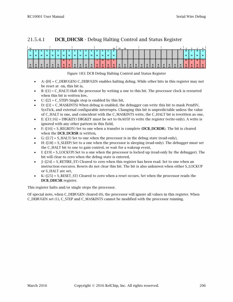
RC10001 User Manual Serial Wire Debug
March 2016 Copyright © 2016 RelChip, Inc. All rights reserved. 206
21.5.4.1 DCB_DHCSR - Debug Halting Control and Status Register
Figure 183: DCB Debug Halting Control and Status Register
A: ([0] = C_DEBUGEN) C_DEBUGEN enables halting debug. While other bits in this register may not be reset at on, this bit is,
B: ([1] = C_HALT) Halt the processor by writing a one to this bit. The processor clock is restarted when this bit is written low,
C: ([2] = C_STEP) Single step is enabled by this bit, D: ([3] = C_MASKINTS) When debug is enabled, the debugger can write this bit to mask PendSV,
SysTick, and external configurable interrupts. Changing this bit is unpredictable unless the value of C_HALT is one, and coincident with the C_MASKINTS write, the C_HALT bit is rewritten as one,
E: ([31:16] = DBGKEY) DBGKEY must be set to 0xA05F to write the register (write-only). A write is ignored with any other pattern in this field,
F: ([16] = S_REGRDY) Set to one when a transfer is complete (DCB_DCRDR). The bit is cleared when the DCB_DCRSR is written,
G: ([17] = S_HALT) Set to one when the processor is in the debug state (read-only), H: ([18] = S_SLEEP) Set to a one when the processor is sleeping (read-only). The debugger must set
the C_HALT bit to one to gain control, or wait for a wakeup event, I: ([19] = S_LOCKUP) Set to a one when the processor is locked up (read-only by the debugger). The
bit will clear to zero when the debug state is entered, J: ([24] = S_RETIRE_ST) Cleared to zero when this register has been read. Set to one when an
instruction executes. Resets do not clear this bit. The bit is also unknown when either S_LOCKUP or S_HALT are set,
K: ([25] = S_RESET_ST) Cleared to zero when a reset occurs. Set when the processor reads the DCB_DHCSR register.
This register halts and/or single steps the processor.
Of special note, when C_DEBUGEN cleared (0), the processor will ignore all values in this register. When C_DEBUGEN set (1), C_STEP and C_MASKINTS cannot be modified with the processor running.
1516E
W
D
R(0)
3D
W
C
R(0)
2C
W
F
R(0)
14
R(0)
R(0)
R(0)
R(0)
R(0)
R(0)
R(0)
R(0)
R(0)
R(0)
4
R(0)
E
W
G
R(0)
H
R(0)
I
R(0)
J
R(1)
K
R(0)
31E
W
B
R(0)
1B
W
A
R(0)
0A
W
E
W
E
W
E
W
E
W
E
W
E
W
E
W
E
W
E
W
E
W
E
W
E
W
E
W
R(0)
R(0)
R(0)
R(0)
R(0)
R(0)
R(0)
R(0)
R(0)
R(0)
R(0)
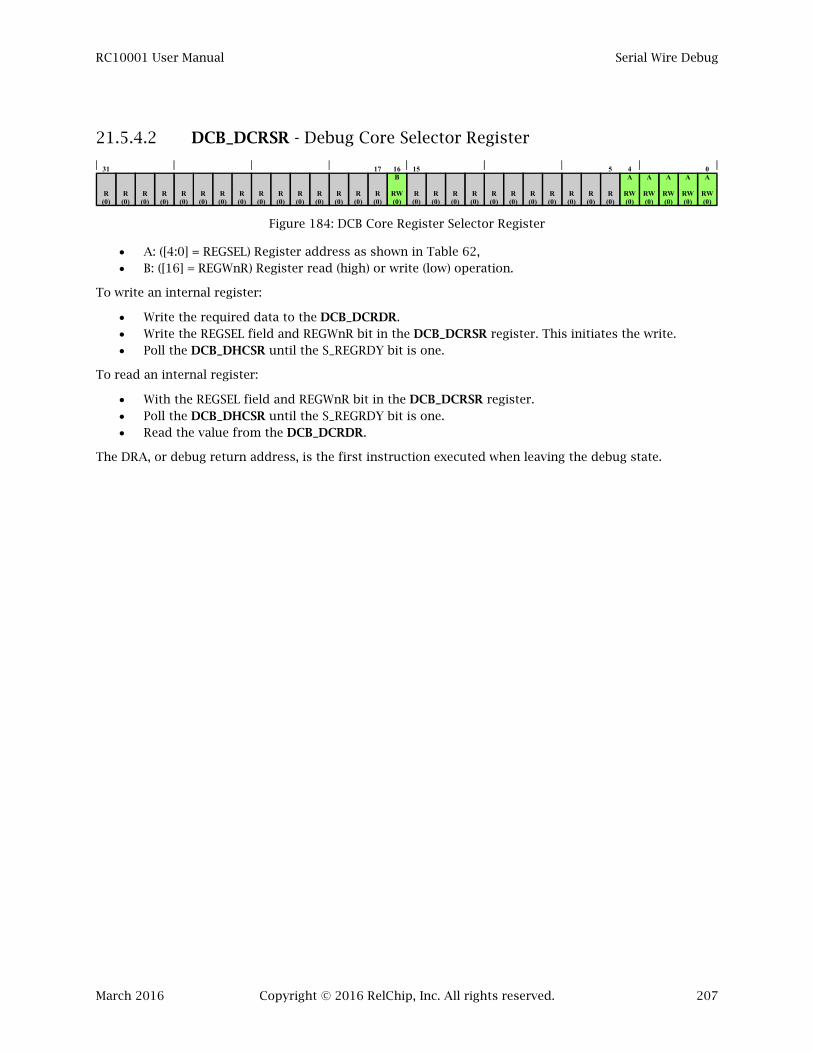
RC10001 User Manual Serial Wire Debug
March 2016 Copyright © 2016 RelChip, Inc. All rights reserved. 207
21.5.4.2 DCB_DCRSR - Debug Core Selector Register
Figure 184: DCB Core Register Selector Register
A: ([4:0] = REGSEL) Register address as shown in Table 62, B: ([16] = REGWnR) Register read (high) or write (low) operation.
To write an internal register:
Write the required data to the DCB_DCRDR. Write the REGSEL field and REGWnR bit in the DCB_DCRSR register. This initiates the write. Poll the DCB_DHCSR until the S_REGRDY bit is one.
To read an internal register:
With the REGSEL field and REGWnR bit in the DCB_DCRSR register. Poll the DCB_DHCSR until the S_REGRDY bit is one. Read the value from the DCB_DCRDR.
The DRA, or debug return address, is the first instruction executed when leaving the debug state.
R(0)
R(0)
R(0)
R(0)
R(0)
R(0)
R(0)
R(0)
R(0)
17
R(0)
R(0)
R(0)
R(0)
R(0)
R(0)
R(0)
R(0)
5
R(0)
0A
RW(0)
R(0)
R(0)
31
R(0)
R(0)
R(0)
R(0)
R(0)
15
R(0)
A
RW(0)
A
RW(0)
A
RW(0)
4A
RW(0)
16B
RW(0)

RC10001 User Manual Serial Wire Debug
March 2016 Copyright © 2016 RelChip, Inc. All rights reserved. 208
Table 62: Register Selection
REGSEL Symbol Access Description Reset
5b00000 R0 RO General Purpose R0 0x??
5b00001 R1 RO General Purpose R1 0x1
5b00010 R2 RO General Purpose R2 0x??
5b00011 R3 RO General Purpose R3 0x1
5b00100 R4 RO General Purpose R4 0x??
5b00101 R5 RO General Purpose R5 0x1
5b00110 R6 RO General Purpose R6 0x??
5b00111 R7 RO General Purpose R7 0x1
5b01000 R8 RO General Purpose R8 0x??
5b01001 R9 RO General Purpose R9 0x1
5b01010 R10 RO General Purpose R10 0x??
5b01011 R11 RO General Purpose R11 0x1
5b01100 R12 RO General Purpose R12 0x??
5b01101 SP RO Current Stack Pointer 0x1
5b01110 LR RO Link Register 0x??
5b01111 DRA RO Debug Return Address 0x1
5b10000 xPSR Status Register
5b10001 MSP Main Stack Pointer
5b10010 PSP Process Stack Pointer
5b10011 - - Reserved
5b10100 CPM CONTROL and PRIMASK Packed
5b10101 to
5b11111 - - Reserved
Table 63: CPM Register Packing
CPM Symbol Access Description Reset
[31:24] CONTROL RO Control Register 0x??
[23:8] - - Reserved 0x??
[7:0] PRIMASK RO Priority Mask 0x??
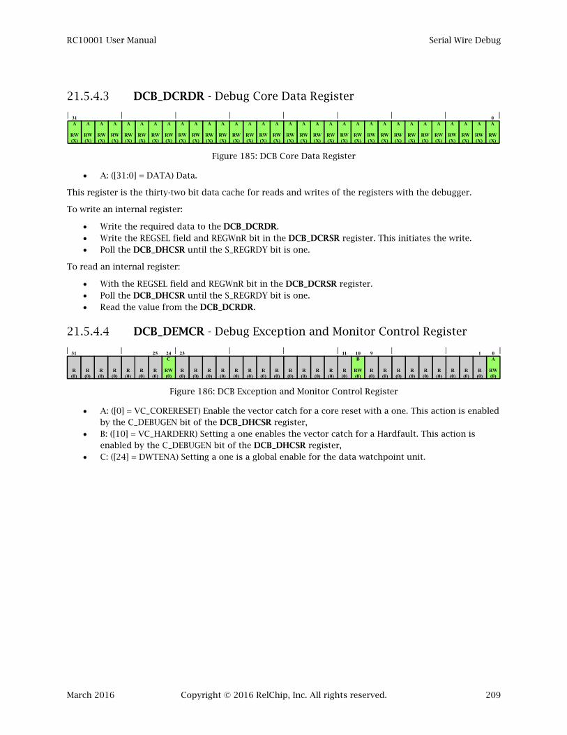
RC10001 User Manual Serial Wire Debug
March 2016 Copyright © 2016 RelChip, Inc. All rights reserved. 209
21.5.4.3 DCB_DCRDR - Debug Core Data Register
Figure 185: DCB Core Data Register
A: ([31:0] = DATA) Data.
This register is the thirty-two bit data cache for reads and writes of the registers with the debugger.
To write an internal register:
Write the required data to the DCB_DCRDR. Write the REGSEL field and REGWnR bit in the DCB_DCRSR register. This initiates the write. Poll the DCB_DHCSR until the S_REGRDY bit is one.
To read an internal register:
With the REGSEL field and REGWnR bit in the DCB_DCRSR register. Poll the DCB_DHCSR until the S_REGRDY bit is one. Read the value from the DCB_DCRDR.
21.5.4.4 DCB_DEMCR - Debug Exception and Monitor Control Register
Figure 186: DCB Exception and Monitor Control Register
A: ([0] = VC_CORERESET) Enable the vector catch for a core reset with a one. This action is enabled by the C_DEBUGEN bit of the DCB_DHCSR register,
B: ([10] = VC_HARDERR) Setting a one enables the vector catch for a Hardfault. This action is enabled by the C_DEBUGEN bit of the DCB_DHCSR register,
C: ([24] = DWTENA) Setting a one is a global enable for the data watchpoint unit.
0A
RW(X)
A
RW(X)
A
RW(X)
A
RW(X)
A
RW(X)
A
RW(X)
A
RW(X)
A
RW(X)
A
RW(X)
A
RW(X)
A
RW(X)
A
RW(X)
A
RW(X)
A
RW(X)
A
RW(X)
A
RW(X)
A
RW(X)
A
RW(X)
A
RW(X)
A
RW(X)
A
RW(X)
A
RW(X)
A
RW(X)
A
RW(X)
A
RW(X)
A
RW(X)
A
RW(X)
A
RW(X)
A
RW(X)
A
RW(X)
A
RW(X)
31A
RW(X)
0A
RW(0)
10B
RW(0)
24C
RW(0)
1
R(0)
R(0)
R(0)
R(0)
R(0)
R(0)
R(0)
R(0)
9
R(0)
11
R(0)
R(0)
R(0)
R(0)
R(0)
R(0)
R(0)
R(0)
R(0)
R(0)
R(0)
R(0)
23
R(0)
25
R(0)
R(0)
R(0)
R(0)
R(0)
R(0)
31
R(0)

RC10001 User Manual Glossary
March 2016 Copyright © 2016 RelChip, Inc. All rights reserved. 210
22 GLOSSARY
AP: Access Port.
APSR: Application Program Status Register.
Byte: An eight bit unsigned integer.
CONTROL: In the core, the control and status register.
Cortex-M0: ARM Processor Core.
DP: Debug Port.
EAPSR: Execution and Application Program Status Register.
EBCFG: External Data Bus Configuration.
EINT: External Data Bus Interrupt.
Endian: Term for the ordering of bits, bytes, halfwords, or word. Big endian is defined as beginning with the most significant digit and ordering in declining significance. Little endian is the opposite, beginning with the least significant digit.
EPSR: Execution Program Status Register.
EXBUS: External Data Bus.
Exception: An anomaly during microcontroller operation.
FIFO: First-In, First-Out Buffer
GPIO: General Purpose Input/Output.
GPIO 0: General Purpose Input/Output Peripheral 0 (twelve pins).
GPIO 1: General Purpose Input/Output Peripheral 1 (twelve pins).
GPIO 2: General Purpose Input/Output Peripheral 2 (twelve pins).
GPIO 3: General Purpose Input/Output Peripheral 3 (twelve pins).
GPIO 4: General Purpose Input/Output Peripheral 4 (twelve pins).
GPIO 5: General Purpose Input/Output Peripheral 5 (twelve pins).
GPIO 6: General Purpose Input/Output Peripheral 6 (twelve pins).
GPIO 7: General Purpose Input/Output Peripheral 7 (six pins).
Halfword: A sixteen bit unsigned integer.
Handler Mode: A Processor mode generally used by operating system and always used by the interrupt service routines. Separate stack pointers are maintained for thread and handler modes.
Hardfault: Exception taken when serious errors occur, such as: illegal instruction, memory access violations, and others.
HARDRESETn: Hard reset input pin.
Interrupt: Asynchronous events that can be used to interrupt program flow.
IAPSR: Interrupt and Application Program Status Register.
IEPSR: Interrupt and Execution Program Status Register.
RC10001 User Manual Glossary
March 2016 Copyright © 2016 RelChip, Inc. All rights reserved. 211
IO: Input/Output.
IOCON: Input/Output Configuration.
IPSR: Interrupt Program Status Register.
ISR: Interrupt Service Routine
LR: Link Register
Memory: Devices to store programs and data for the microcontroller.
Memory-mapped: A system where all devices, peripheral and memory, are mapped into the memory address space.
Microcontroller: A device including a processor, memory and peripheral IO device(s).
MSP: Main Stack Pointer Register.
NMI: Non-Maskable Interrupt.
NVIC: Nested Vectored Interrupt Controller.
PC: Program Counter.
PendSV: Pending Service Call Interrupt.
Peripheral: Input/Output device to connect a microcontroller to its environment.
Pipeline: In the microcontroller, a pipeline creates stages (fetch, execute and writeback) that all operate on the same clock cycle. The controller fetches the next instruction, executes the current one, and writes back the results at the same time. Each stage of the pipeline is the input for the following stage.
POR: Power on Reset.
PPB: Private Peripheral Bus
PRIMASK: Priority Mask Register.
Processor: The core computational engine of a microcontroller.
PSP: Process Stack Pointer Register.
PSR: Program Status Register.
R#: General Purpose Register.
RAM: Random Access Memory.
RAMCFG: RAM Configuration.
ROM: Read Only Memory.
RTC: Real Time Counter.
Sleep Mode: An execution mode where most of the microcontroller is powered down, waiting for some event to “wake it up.” This is very useful to control power consumption in microcontroller-based systems.
SOFTRESETn: Soft reset external pin.
SP: Stack Pointer.
SPI: Serial Peripheral Interface.
SSP: Synchronous Serial Peripheral.
Stack Pointer: A register pointing at a memory location that “stacks” return address and data values for subroutine calls.

RC10001 User Manual Glossary
March 2016 Copyright © 2016 RelChip, Inc. All rights reserved. 212
SVCall: Service Call Interrupt.
SVC1: Service 1 Interrupt.
SVC2: Service 2 Interrupt.
SWD: Serial Wire Debug.
SYSCON: System Configuration.
SysTick: System Tick Timer.
Thread Mode: The mode used by user applications so that the operating system stack is not corrupted by application errors. A separate stack is maintained to avoid corruption.
TIM16A: 16-Bit Timer/Counter.
TIM16B: 16-Bit Timer/Counter.
TIM32A: 32-Bit Timer/Counter.
TIM32B: 32-Bit Timer/Counter.
UART: Universal Asynchronous Receiver/Transmitter.
WAKEUP: Interrupt generated by the external pin.
WDT: Watchdog Timer.
Word: A thirty-two bit unsigned integer value.
XPSR: Application, Execution, and Interrupt Program Status Register
RC10001 User Manual Index
March 2016 Copyright © 2016 RelChip, Inc. All rights reserved. 213
23 INDEX
Assembly ADCS (Add with Carry) ....................................... 47 ADD .......................................................... 47, 48, 49 ADDS (w Flags) .............................................. 50, 51 ADR (Add PC) ........................................................ 51 ANDS (Bitwise) ...................................................... 52 ASRS (Arith Shift Right) ............................... 53, 54 B (Branch Unconditional) .................................... 54 B[c] (Branch Conditional) .................................... 55 BICS (Bitwise Comp AND) ................................... 56 BKPT (Breakpoint) ................................................ 56 BL (Branch with Link) .......................................... 57 BLX (Branch with Link & Exchange) .................. 57 BX (Branch with Exchange) ................................. 58 CMN (Compare Negative) ................................... 58 CMP (Compare) ..................................................... 59 CPSID (Disable PRIMASK) ................................... 60 CPSIE (Enable PRIMASK) ..................................... 60 DMB (Data Memory Barrier) ............................... 60 DSB (Data Synch Barrier) .................................... 61 EORS (Bitwise XOR) .............................................. 61 ISB (Inst Synch Barrier) ....................................... 62 LDM (Load Multiple) ..................................... 62, 63 LDMFD (Load Multiple) ....................................... 63 LDMIA (Load Multiple) ........................................ 63 LDR (Load) ...................................................... 64, 65 LDRB (Load Byte) .................................................. 66 LDRH (Load HalfWord)........................................ 67 LDRSB (Load Signed Byte) .................................. 68 LDRSH (Load Signed HalfWord) ........................ 68 LSLS (Shift Left) ............................................. 69, 70 LSRS (Shift Right) .......................................... 70, 71 MOV (Move) ........................................................... 71 MOVS (Move w Flags) .......................................... 72 MRS (Move Special) .............................................. 73 MSR (Move Special) .............................................. 74 MULS (Multiply) .................................................... 74 MVNS (Move Bitwise NOT) .................................. 75 NOP ......................................................................... 75 ORRS (Bitwise OR) ................................................ 76 POP .......................................................................... 76 PUSH ....................................................................... 77 REV (Reverse Byte) ............................................... 77 REV16 (Reverse Byte) .......................................... 78 REVSH (Reverse Byte) .......................................... 78 RORS (Rotate Right) ............................................. 79 RSBS (Reverse Subtract) ...................................... 80 SBCS (Subtract w Carry) ...................................... 80 SEV (NOP) ............................................................... 81 STM (Store Multiple) ..................................... 81, 82 STMEA (Store Multiple) ....................................... 82 STMIA (Store Multiple) ........................................ 82 STR (Store) ...................................................... 83, 84 STRB (Store Byte) ........................................... 84, 85 STRH (Store HalfWord) ................................ 85, 86
SUB (Subtract w Flags) ................................. 87, 88 SUB (Subtract) ................................................ 86, 87 SVC (Supervisor Call) .......................................... 89 SXTB (Sign Extend Byte) ...................................... 89 SXTH (Sign Extend HalfWord) ............................ 90 TST (Test Registers) ............................................. 90 UXTB (Extend Byte) .............................................. 91 UXTB (Extend HalfWord) .................................... 91 WFE (Wait for Event) ............................................ 92 WFI (Wait for Interrupt) ...................................... 92
Clock Generator (CLKOUT) ................................. 182 Cortex-M0
Application Program Status Register (APSR) . 23 Control Register (CONTROL) ............................ 24 Execution Program Status Register (EPSR) ..... 23 Interrupt Program Status Register (IPSR) ....... 23 Pipeline ........................................................... 20, 34 Priority Mask Register (PRIMASK) .................... 23 Program Status Register (PSR) .......................... 22
Exceptions and Interrupts ..................................... 25 Active .................................................................. 202 Chaining ................................................................. 32 Debug .................................................202, 204, 206 Enables . 101, 102, 119, 120, 121, 122, 133, 134,
142, 144, 157, 158, 166, 169, 170, 177, 178, 180
EXBUS .................................................129, 133, 134 GPIO ....................................................113, 119, 120 Hard Fault .............................................................. 27 ISR Entry and Exit ................................................ 30 Multiple Word Operations .................................. 31 NMI ......................................................................... 27 NVIC ....................................................................... 99 Pending ............................................................... 104 Peripheral .............................................................. 28 Priority .......................................... 27, 99, 105, 106 RAM ............................................................ 121, 122 Reset ....................................................................... 30 Return .................................................................... 31 RTC ...................................................................... 177 Software ................................................................. 99 SSP ............................................................... 157, 158 Supervisor Call ..................................................... 28 System Tick Timer ............................................... 28 SysTick ................................................................ 180 Timers ................................................166, 169, 170 UART ..................................................136, 142, 144 Vector Catch ...................................................... 209 WDT ..................................................................... 178
External Bus Configuration (EBCFG) ................. 124 32-Bit .......................................................... 125, 127 8-Bit ..................................................................... 129 Bus Configuration (BUS_CONFIG) ................. 132 Configuration (CONFIG) .................................. 131 Configuration and Status ................................ 128
RC10001 User Manual Index
March 2016 Copyright © 2016 RelChip, Inc. All rights reserved. 214
Error Configuration (ERR_CONFIG) .............. 134 Interrupt Clear (ICR) ........................................ 134 Interrupt Enable (IE) ......................................... 133 Interrupts ........................................................... 129 Masked Interrupt Status (MIS) ........................ 133 Min and Max CS (MINx,MAXx) ....................... 134 Parity ................................................................... 128 Pinout .................................................................. 124 Raw Interrupt Status (RIS) .............................. 133 SMP ...................................................................... 130 Wait ...................................................................... 129
General Purpose IO (GPIO) .................................. 113 Data (DATA) ...................................................... 116 Direction (DIR) .................................................. 116 Interrupt Both Edges (IBE) .............................. 117 Interrupt Clear (ICR) ........................................ 120 Interrupt Enable (IE) ......................................... 119 Interrupt Event (IEV) ........................................ 118 Interrupt Sense (IS) ........................................... 117 Masked Interrupt Status (MIS) ........................ 120 Raw Interrupt Status (RIS) .............................. 119 Read ..................................................................... 114 Write .................................................................... 113
Interrupt Control (NVIC) ........................ 18, 99, 201 Clear Pending (ICPR) ........................................ 104 Disable Interrupt (ICER) .................................. 102 Enable Interrupt (ISER) .................................... 101 Priority (IPR0) .................................................... 105 Priority (IPR1) .................................................... 105 Priority (IPR2) .................................................... 105 Priority (IPR3) .................................................... 106 Priority (IPR4) .................................................... 106 Priority (IPR5) .................................................... 106 Set Pending (ISPR) ............................................. 103
Interrupt priority .................................................. 204 IO Configuration (IOCON) ................................... 107 Power Management ................................. 36, 39, 203
Clock Enable ......................................................... 96 Program Counter ................................... 22, 197, 198 RAM Configuration .............................................. 121
Interrupt Clear (ICR) ........................................ 122 Interrupt Enable (IE) ......................................... 121 Masked Interrupt Status (MIS) ........................ 122 Raw Interrupt Status (RIS) .............................. 122 Test Mode (TM) ................................................. 123
Real Time Counter ................................................ 174 Alarm (ALM) ...................................................... 176 Interrupt Clear (ICR) ........................................ 177 Interrupt Enable (IE) ......................................... 177 Masked Interrupt Status (MIS) ........................ 177 Mode (MOD) ....................................................... 174 Per-Scale Counter (PC) ..................................... 176 Pre-Scale Load (PR) ........................................... 175 Raw Interrupt Status (RIS) .............................. 177 Time (TIM) .......................................................... 175
Serial Interface (SSP) ............................................ 150 Control 0 (CR0) ................................................. 154 Control 1 (CR1) ................................................. 155 FIFO Clear (FCLR) .............................................. 159 FIFO Count (FCNT) ........................................... 158
Interrupt Clear (ICR) ........................................ 158 Interrupt Enable (IE) ......................................... 157 Masked Interrupt Status (MIS) ........................ 158 Pinout .................................................................. 150 Prescale (PR) ...................................................... 156 Protocols ............................................................. 151
Microwire ........................................................ 153 Serial Peripheral Interface ........................... 151
Clock Control ............................................. 151 Synchronous Serial Interface ...................... 152
Raw Interrupt Status (RIS) .............................. 157 Status (SR) .......................................................... 156 TX/RX FIFO (DR) ............................................... 156
Serial Wire Debug (DAP) ...................................... 183 Access Port ......................................................... 194
Banked Data (BD#) ........................................ 195 Configuration (CFG) ..................................... 195 Control and Status (CSW) ............................ 194 Data Read/Write (DRW) ............................... 195 Debug Base Address (BASE) ........................ 196 Identification (IDR) ....................................... 196 Transfer Address (TAR) .............................. 195
Debug Port ......................................................... 191 Abort (ABORT) .............................................. 192 Control and Status (CTRL/STAT) .............. 192 Identification Code (IDCODE) .................... 191 Read Buffer (RDBUFF) .................................. 192 Resend (RESEND) .......................................... 193 Select (SELECT) .............................................. 193 Wire Control (WCR) ...................................... 192
Parity Error ......................................................... 190 Protocol ............................................................... 184
Acknowledge .................................................. 185 Data .................................................................. 185 FAULT Ack ...................................................... 189 Host Read ....................................................... 186 Host Write ....................................................... 185 Posted Reads .................................................. 186 Request ........................................................... 184 RESEND ........................................................... 187 Turnaround .................................................... 184 WAIT Ack ........................................................ 188
Protocol Error .................................................... 190 Reset .................................................................... 183 Sticky Flags ........................................................ 190
Stack Pointer ............................................................. 21 Align ....................................................................... 23 Main .......................................................... 20, 21, 24 Process ............................................................ 20, 21
System Configuration (SYSCON)........................... 93 Battery Backup (BATTCTRL) ............................. 98 Boot Control (BOOTCTRL) ................................. 94 CLKOUT Division (CLKOUTDIV) ...................... 97 Clock Division (AHBCLKDIV) ............................ 97 Clock Enable (AHBCLKCTRL) .. 37, 96, 107, 113,
136, 138, 150, 160, 178 Device ID (DEVICEID) ......................................... 98 Peripheral Reset (PRESETCTRL) ....................... 94 Reset Source (RSTSTAT) .................................... 95 System Tick Calibration (SYSTCKCAL) .. 97, 181

RC10001 User Manual Index
March 2016 Copyright © 2016 RelChip, Inc. All rights reserved. 215
System Tick Timer (SysTick) ........................ 28, 180 Calibration (CALIB) .......................................... 181 Control and Status (CTRL) .............................. 180 Current Value (VAL) ......................................... 181 Reload Value (LOAD) ....................................... 181
Timer/Counter ...................................................... 160 Capture Control (CCR) ..................................... 170 Capture Value (CR0) ......................................... 171 Control (TCR) .................................................... 166 External Match (EMR) ....................................... 171 Interrupt Enable (IR) ......................................... 166 Match ................................................................... 161
Capture ........................................................... 164 Events .............................................................. 161 External ........................................................... 163 LIN Counter .................................................... 164 Operation ........................................................ 161
Match (MR#) ....................................................... 170 Match Control (MCR) ........................................ 169 Match Output (MOR) ........................................ 173 Match Output Control (MOCR) ...................... 173 Pre-Scale Counter (PC) ..................................... 168 Pre-Scale Divisor (PR) ....................................... 167 Pulse Width Modulator (PWMC) ..................... 172 Timer Control (CTCR) ...................................... 172 Timer Counter (TC) .......................................... 167
UART ....................................................................... 136 Divisor Latch (DLL) ........................................... 141 Divisor Latch (DLM) .......................................... 141 FIFO Control (FCR)............................................ 143
Interrupt Enable (IE) ......................................... 142 Interrupt Identification (IIR) ........................... 144 LIN Control (LCTL) ........................................... 149 Line Control (LCR) ............................................ 145 Line Status (LSR) ............................................... 147 Modem Control (MCR) ..................................... 146 Modem Status (MSR) ........................................ 147 Modes .................................................................. 136
LIN .................................................................... 138 Master .......................................................... 138 Slave ............................................................. 139
RS-232 ............................................................. 137 RS-485 ............................................................. 137
Address Auto Detection ........................... 137 Auto Direction Control ............................ 138 Normal Multidrop...................................... 137
Pinout .................................................................. 139 Receive Buffer (RBR) ........................................ 142 RS-485 Address Match (RS485ADDR) .......... 149 RS-485 Control (RS485CTRL) ......................... 148 Scratch (SCR) ..................................................... 148 Transmit Enable (TER) ..................................... 148 Transmit Holding (THR) .................................. 141 Turnaround Delay (RS485DLY) ..................... 149
Watchdog Timer (WDT) ................................. 39, 178 Feed (FEED) ........................................................ 179 Mode (MOD) ....................................................... 178 Time Out (TC) .................................................... 179 Timer Value (TV) ............................................... 179

RC10001 User Manual Index
March 2016 Copyright © 2016 RelChip, Inc. All rights reserved. 216
Disclaimer: RELCHIP, Inc. MAKES NO REPRESENTATIONS OR WARANTIES, EITHER EXPRESS OR IMPLIED, OR MERCHANTABILITY OR FITNESS FOR A PARTICULAR PURPOSE OR OF ANY NATURE REGARDING THE INFORMATION IN THIS DOCUMENT OR THE PRODUCT TO WHICH THE DOCUMENT REFERS. RelChip will not be held liable for direct, indirect, special, incidental, consequential or any other damages, without limitation, for the use of this information, or the products described. The information in this document may include errors. RelChip reserves the right to make product improvements.

![Interrupt Priorities Soþuare via Interrupt - USENIX · Setting Interrupt Priorities in Soþuare via Interrupt Queueing Geoff Collyer Bell Laboratories ... [Kernighan & Ritchie 1978]](https://img.dokumen.tips/doc/110x75/5c8a77bf09d3f22e408bf5b1/interrupt-priorities-sobuare-via-interrupt-usenix-setting-interrupt-priorities.jpg)