Embed Size (px)
Citation preview

Reference Receiver Based Digital
Self-Interference Cancellation in
MIMO Full-Duplex Transceivers
Dani Korpi, Lauri Anttila, and Mikko Valkama
Tampere University of Technology, Department of Electronics and
Communications Engineering, Finland
10th International Workshop on Broadband Wireless Access

Outline
• Introduction
• RF impairments in a full-duplex transceiver
• Reference receiver based structure
• Initial analysis with system calculations
• Reference receiver aided digital cancellation
procedure
• Waveform simulations
• Conclusion
2
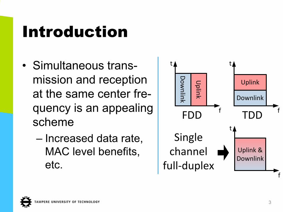
Introduction
• Simultaneous trans-
mission and reception
at the same center fre-
quency is an appealing
scheme
– Increased data rate,
MAC level benefits,
etc.
3
f
t
f
t
Do
wn
link
Up
link
Uplink
Downlink
FDD TDD
f
t
Uplink & Downlink
Single channel
full-duplex

Introduction (cont.)
4
• However, it has
also its down-
sides
– Increased com-
plexity due to
self-interference
cancellation, RF
impairments,
etc.
Receiver chain
Transmitter chain
Tx
RxS
elf-in
terf
ere
nce
RF cancellation Digital cancellation
DAC
ADC
SI regenerationAttenuation
& delay
PA

RF impairments
• The self-interference (SI) signal is distorted in
numerous ways within the transceiver chain,
especially in the transmitter
– This affects the accuracy with which the SI
signal can be regenerated for cancellation in
the digital domain
– Advanced modeling is required to achieve a
sufficient amount of SI cancellation
5
Reference receiver based
structure
6
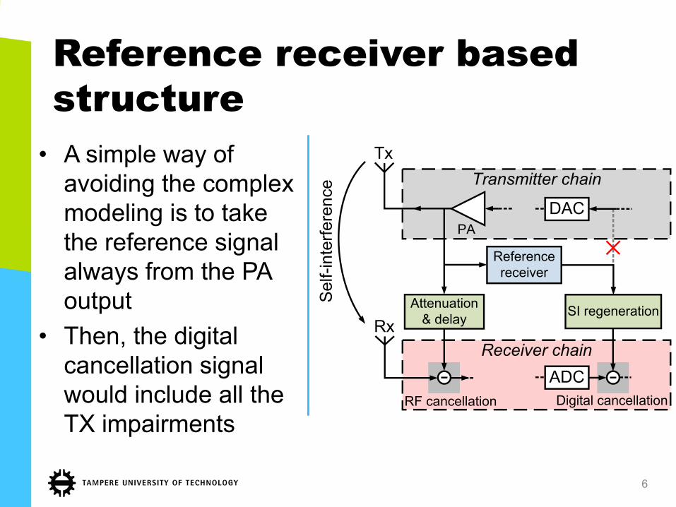
• A simple way of
avoiding the complex
modeling is to take
the reference signal
always from the PA
output
• Then, the digital
cancellation signal
would include all the
TX impairments
Receiver chain
Transmitter chain
Tx
RxS
elf-in
terf
ere
nce
RF cancellation Digital cancellation
DAC
ADC
SI regenerationAttenuation
& delay
PA
Reference
receiver

Reference receiver based
structure (cont.)
• The downside of this approach is the need for
additional receivers
– In essence, a trade-off between the
computational cost of digital cancellation and
RF hardware
• It is not obvious what is the optimal scheme
of utilizing the additional receivers
7
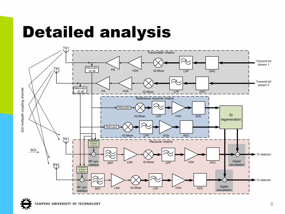
Detailed analysis
8
Receiver chainsAmplitude
& phase
matching
RF can-
cellation
Reference receiver chains
Transmitter chains
TX2
BPF LNA IQ Mixer LPF VGA
2x2
mu
ltip
ath
co
up
ling
ch
an
ne
l
ADC
LPFIQ MixerVGAPA DAC
Digital
cancellation
To detector
TX1
LPFIQ MixerVGAPADAC
Transmit bit
stream 1
Transmit bit
stream 2
BPF LNA IQ Mixer LPF VGA ADC
Amplitude
& phase
matching
Digital
cancellationRF can-
cellation
To detector
Attenuator
IQ Mixer VGA ADC
Attenuator
IQ Mixer ADCVGA
Attenuator
-30 dB
Attenuator
-30 dB
SI
regeneration
RX1
RX2
LPF
LPF
SOI

Initial performance comparison
with system calculations
3.12.2014 9
With the reference receiver based structure, even linear processing can
provide sufficient SI suppression with transmit powers up to 20-25 dBm.
-5 0 5 10 15 20 25-90
-80
-70
-60
-50
-40
-30
-20
-10
0
Transmit power (dBm)
Pow
er
of diff
ere
nt sig
nal c
om
ponents
(dB
m)
Linear Digital Cancellationwith Reference Receivers
-5 0 5 10 15 20 25-90
-80
-70
-60
-50
-40
-30
-20
-10
0
Transmit power (dBm)
Pow
er
of diff
ere
nt sig
nal c
om
ponents
(dB
m)
Traditional LinearDigital Cancellation
SI mirror image
Noise floor
Quantization noise
TX-induced nonlinearities
RX-induced nonlinearities
Signal of interest
SI mirror image
Noise floor
Quantization noise
RX-induced nonlinearities
Signal of interest

Reference receiver aided
cancellation procedure
• The digital cancellation procedure is very
straight-forward in this case
• The received SI signal in the digital domain
during the training period can be expressed as
𝐬𝑖,𝐴𝐷𝐶,𝑡𝑟 = 𝐗𝑗,𝑃𝐴,𝑡𝑟
𝑁𝑇
𝑗=1
𝐡𝑖𝑗 + 𝐳𝑖,𝑡𝑟 = 𝐗𝑃𝐴,𝑡𝑟𝐡𝑖 + 𝐳𝑖,𝑡𝑟.
• Each 𝐗𝑗,𝑃𝐴,𝑡𝑟 is constructed from the samples
obtained via the reference receivers
3.12.2014 10

Parameter estimation
• For example, least squares can be used to
estimate the SI channel:
𝐡 𝑖 = 𝐗𝑃𝐴,𝑡𝑟𝐻 𝐗𝑃𝐴,𝑡𝑟
−1𝐗𝑃𝐴,𝑡𝑟
𝐻 𝐬𝑖,𝐴𝐷𝐶,𝑡𝑟
• Using 𝐡 𝑖, a cancellation signal can be
generated for any given transmit signal,
which is then used to cancel the SI:
𝐲𝑖,𝐷𝐶 = 𝐬𝑖,𝐴𝐷𝐶 + 𝐫𝑖 − 𝐗𝑃𝐴𝐡 𝑖 ≈ 𝐫𝑖 + 𝐳𝑖 ,
where 𝐫𝑖 is the signal of interest.
4.12.2014 11

Waveform simulations
8.12.2014 12
• More comprehensive
performance analysis
using the same
transceiver model as
earlier
• Explicit baseband-
equivalent model for
each component,
resulting in realistic
distortion of the SI
signal
Receiver chainsAmplitude
& phase
matching
RF can-
cellation
Reference receiver chains
Transmitter chains
TX2
BPF LNA IQ Mixer LPF VGA
2x2
mu
ltip
ath
co
up
ling
ch
an
ne
l
ADC
LPFIQ MixerVGAPA DAC
Digital
cancellation
To detector
TX1
LPFIQ MixerVGAPADAC
Transmit bit
stream 1
Transmit bit
stream 2
BPF LNA IQ Mixer LPF VGA ADC
Amplitude
& phase
matching
Digital
cancellationRF can-
cellation
To detector
Attenuator
IQ Mixer VGA ADC
Attenuator
IQ Mixer ADCVGA
Attenuator
-30 dB
Attenuator
-30 dB
SI
regeneration
RX1
RX2
LPF
LPF
SOI

Waveform simulations (cont.)
• The proposed
scheme cancels
SI efficiently
• With the higher
transmit powers,
it is limited by
the impairments
of the receiver
chains
8.12.2014 13
-5 0 5 10 15 20 25-20
-15
-10
-5
0
5
10
15
Transmit Power (dBm)
SIN
R (
dB
)
Reference RX aided cancellation
Linear cancellation
Widely-linear cancellation
Nonlinear cancellation

Conclusion
• The proposed reference receiver based
scheme achieves a significant improvement
in the SI cancellation ability utilizing only
simple linear processing in the digital domain
• However, it requires additional hardware in
the RF domain
• Additional research is required to assess
whether this is the best way of using the
additional receivers
3.12.2014 14

Thank you
• Questions and/or comments are welcome!
3.12.2014 15