Embed Size (px)
Citation preview

Power Integrations
5245 Hellyer Avenue, San Jose, CA 95138 USA. Tel: +1 408 414 9200 Fax: +1 408 414 9201
www.powerint.com
Title Reference Design Report for a 10 W CV/ CC USB Charger using InnoSw itchTM-CH INN2023K
Specification 85 VAC – 264 VAC Input; 5 V, 2 A Output (end of USB Cable)
Application Cell Phone / USB Charger
Author Applications Engineering Department
Document Number RDR-420
Date April 20, 2015
Revision 1.1 Summary and Features • InnoSwitch-CH - Industry first AC/DC ICs with isolated, safety rated integrated
feedback • All the benefits of secondary side control with the simplicity of primary side regulation
• ±3% CV, ±5% CC regulation • Insensitive to transformer variation • Transient response independent of load timing • Smaller, lower cost output capacitors • <10 mW no-load input power • Cable voltage drop compensation
• Built in synchronous rectification for high efficiency PATENT INFORMATION The products and applications illustrated herein (including transformer construction and circuits external to the products) may be covered by one or more U.S. and foreign patents, or potentially by pending U.S. and foreign patent applications assigned to Power Integrations. A complete list of Power Integrations' patents may be found at www.powerint.com. Power Integrations grants its customers a license under certain patent rights as set forth at <http://www.powerint.com/ip.htm>.

RDR-420 10 W 5 V, 2 A InnoSwitch-CH USB Charger 20-Apr-15
Page 2 of 51
Power Integrations, Inc. Tel: +1 408 414 9200 Fax: +1 408 414 9201 www.powerint.com
Table of Contents Introduction ......................................................................................................... 4 1 Power Supply Specification ................................................................................... 5 2 Schematic ............................................................................................................ 6 3 Circuit Description ................................................................................................ 7 4
Input EMI Filtering ......................................................................................... 7 4.1 InnoSwitch-CH IC Primary .............................................................................. 7 4.1 InnoSwitch-CH IC Secondary .......................................................................... 8 4.2
PCB Layout .......................................................................................................... 9 5 Bill of Materials .................................................................................................. 11 6 Transformer Specification ................................................................................... 12 7
Electrical Diagram ........................................................................................ 12 7.1 Electrical Specifications ................................................................................ 12 7.2 Materials ..................................................................................................... 12 7.3 Transformer Build Diagram .......................................................................... 13 7.4 Transformer Instructions .............................................................................. 13 7.5 Transformer Illustrations .............................................................................. 14 7.6
Transformer Design Spreadsheet ........................................................................ 18 8 Performance Data .............................................................................................. 21 9
Active Mode Efficiency (at USB Socket) vs. Line ............................................. 21 9.1 Active Mode Efficiency (at USB Socket) vs. Load ............................................ 22 9.2
Efficiency without Schottky Diode in Parallel with Q1, SR FET .................. 22 9.2.1 Efficiency with a Schottky Diode, SS16, in Parallel with Q1, SR FET .......... 24 9.2.2
No-Load Input Power ................................................................................... 25 9.3 Average Efficiency (at USB Socket) ............................................................... 26 9.4
Efficiency Requirements ........................................................................ 26 9.4.1 Average Efficiency at 115 VAC Input ...................................................... 26 9.4.2 Average Efficiency at 230 VAC Input ...................................................... 27 9.4.3
CV/CC Regulation Measured at the End of Cable ............................................ 28 9.5 Open Case Thermal Performance ..................................................................... 29 10 Waveforms ..................................................................................................... 31 11
Load Transient Response (end of cable) ........................................................ 31 11.1 Load Transient Response (at USB Socket) ..................................................... 32 11.2 Switching Waveforms ................................................................................... 33 11.3
InnoSwitch-CH Waveforms .................................................................... 33 11.3.1 SR FET Waveforms ............................................................................... 33 11.3.2
Output Ripple Measurements ........................................................................ 34 11.4 Ripple Measurement Technique ............................................................. 34 11.4.1 Measurement Results ............................................................................ 35 11.4.2
Conductive EMI ............................................................................................... 36 12 2 A Resistive Load, Floating Output (PK / AV) ................................................ 36 12.1 2 A Resistive Load, Artificial Hand Ground (PK / AV) ...................................... 38 12.2 Smartphone with Monitor Set-up (HDMI) (QP / AV) ....................................... 40 12.3

20-Apr-15 RDR-420 10 W 5 V, 2 A InnoSwitch-CH USB Charger
Page 3 of 51
Power Integrations Tel: +1 408 414 9200 Fax: +1 408 414
9201
Radiative EMI ................................................................................................. 42 13 Audible Noise .................................................................................................. 44 14 Lighting Surge & ESD Test ............................................................................... 49 15
Differential Mode Test .................................................................................. 49 15.1 Common Mode Test ..................................................................................... 49 15.2 ESD Test ..................................................................................................... 49 15.3
Revision History .............................................................................................. 50 16 Important Note: Although this board is designed to satisfy safety isolation requirements, the engineering prototype has not been agency approved. Therefore, all testing should be performed using an isolation transformer to provide the AC input to the prototype board.

RDR-420 10 W 5 V, 2 A InnoSwitch-CH USB Charger 20-Apr-15
Page 4 of 51
Power Integrations, Inc. Tel: +1 408 414 9200 Fax: +1 408 414 9201 www.powerint.com
Introduction 1This document is an engineering report describing a 2 A, 5.0 V USB charger utilizing a device from the InnoSwitch-CH family of ICs. This design is intended to show the high power density and efficiency that is possible due to the high level of integration while still providing exceptional performance. This document contains the power supply specification, schematic, bill of materials, transformer documentation, printed circuit layout, and performance data.
Figure 1 – Populated Circuit Board Photograph, Top.
Figure 2 – Populated Circuit Board Photograph, Bottom.

20-Apr-15 RDR-420 10 W 5 V, 2 A InnoSwitch-CH USB Charger
Page 5 of 51
Power Integrations Tel: +1 408 414 9200 Fax: +1 408 414
9201
Power Supply Specification 2The table below represents the minimum acceptable performance of the design. Actual performance is listed in the results section.
Description Symbol Min Typ Max Units Comment Input Voltage VIN 85 265 VAC 2 Wire – no P.E.
Frequency fLINE 50 50/60 64 Hz
No-load Input Power 10 mW 230 VAC
Output
Output Voltage VOUT 4.75 5.0 5.25 V 0.35 V cable resistance drop
Transient Output Voltage VOUT(T) 4.2 5.5 V 0 A - 2 A - 0 A load step end of cable
At the end of the output cable Output Ripple Voltage VRIPPLE 150 mV At the end of the output cable
Output Cable Compensation VCBL 250 300 350 mV At 2 A output current
Output Current CC point IOUT 2 2.5 A
Auto-Restart Voltage VAR 2 3.5 V At end of cable
Turn on Rise Time tR 20 ms
Rated Output Power POUT 10 W
Efficiency
Average 25%, 50%, 75%, and 100%
ηAVE[BRD] 84 % Measured at USB socket
ηAVE[CBL] 80 % With 0.38 V cable resistance drop
10% η10% 79 %
Environmental
Output Cable Impedance RCBL 190 mΩ
Conducted EMI CISPR22B / EN55022B
Load floating or grounded via artificial hand
Resistive load, 6 dB Margin
Connected to mobile phone and TV (MHL connection enabled) 6 dB Margin
Safety IEC950 / UL1950 Class II Designed to meet
Audible noise 25 dB Measured at 3 cm
Line Surge Common mode (L1/L2-PE)
6
kV
Ring Wave, Common Mode: 12 Ω
ESD ±16.5 ±8 kV
kV
Contact
Air discharge No degradation in performance
Ambient Temperature TAMB 0 40 oC Free convection, sea level in sealed enclosure
RDR-420 10 W 5 V, 2 A InnoSwitch-CH USB Charger 20-Apr-15
Page 6 of 51
Power Integrations, Inc. Tel: +1 408 414 9200 Fax: +1 408 414 9201 www.powerint.com
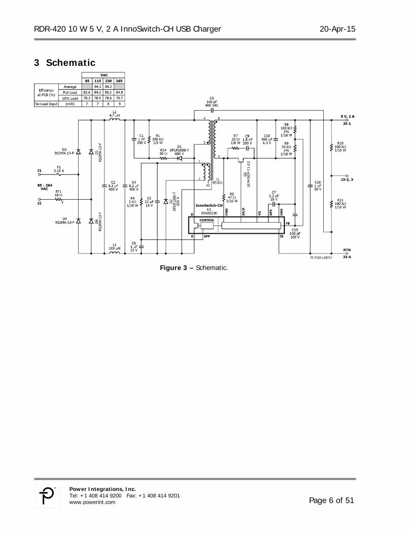
Schematic 3
Figure 3 – Schematic.

20-Apr-15 RDR-420 10 W 5 V, 2 A InnoSwitch-CH USB Charger
Page 7 of 51
Power Integrations Tel: +1 408 414 9200 Fax: +1 408 414
9201
Circuit Description 4
Input EMI Filtering 4.1Fuse F1 provides protection against catastrophic failure of components on the primary side. An inrush limiting thermistor (RT1) was necessary due to the low surge current rating of the rectifier diodes (D1-D4) and the relatively high value and therefore low impedance of the bulk storage capacitors C2 and C4. Physically small diodes were selected for D1-D4 due to the limited space, specifically height from PCB to case. Capacitor C2 and C4 provide filtering of the rectified AC input and together with L1 and L2 form a π (pi) filter to attenuate differential mode EMI. A low value Y capacitor (C8) reduces common mode EMI.
InnoSw itch-CH IC Primary 4.1One side of the transformer primary is connected to the rectified DC bus, the other is connected to the integrated 650 V power MOSFET inside the InnoSwitch-CH IC (U1). A low cost RCD clamp formed by D1, R1, R14 and C1 limits the peak drain voltage due to the effects of transformer and output trace inductance. The IC is self-starting, using an internal high voltage current source to charge the BPP pin capacitor (C6) when AC is first applied. During normal operation the primary side block is powered from an auxiliary winding on the transformer. The output of this is configured as a flyback winding, rectified and filtered (D2 and C5) and fed in the BPP pin via a current limiting resistor R4. Output regulation is achieved using On/Off control, the number of enabled switching cycles are adjusted based on the output load. At high load most switching cycles are enabled, and at light load or no-load most cycled are disabled or skipped. Once a cycle is enabled, the power MOSFET remain on until the primary current ramps to the device current limit for the specific operating state. There are four operating states (current limits) arrange such that the frequency content of the primary current switching pattern remains out of the audible range until at light load where the transformer flux density and therefore audible noise generation is at a very low level.
RDR-420 10 W 5 V, 2 A InnoSwitch-CH USB Charger 20-Apr-15
Page 8 of 51
Power Integrations, Inc. Tel: +1 408 414 9200 Fax: +1 408 414 9201 www.powerint.com
InnoSw itch-CH IC Secondary 4.2The secondary side of the InnoSwitch-CH provides output voltage, output current sensing and drive to a MOSFET providing synchronous rectification. The secondary of the transformer is rectified by Q1 and filtered by C10. High frequency ringing during switching transients that would otherwise create high voltage across Q1 and radiated EMI is reduced via snubber components R7 and C9. To reduce dissipation synchronous rectification (SR) is provided by Q1. The gate of Q1 is turned on based on the winding voltage sensed via R5 and the FWD pin of the IC. In continuous conduction mode operation the power MOSFET is turned off just prior to the secondary side commanding a new switching cycle from the primary. In discontinuous mode the MOSFET is turned off when the voltage drop across the MOSFET falls below a threshold. Secondary side control of the primary side MOSFET ensure that it is never on simultaneously with the synchronous rectification MOSFET. The MOSFET drive signal is output on the SR/P pin. The secondary side of the IC is self-powered from either the secondary winding forward voltage or the output voltage. During CV operation the output voltage powers the device, fed into the VO pin. During CC operation, when the output voltage falls the device will power itself from the secondary winding directly. During the on-time of the primary side MOSFET the forward voltage that appears across the secondary winding is used to charge the decoupling capacitor C7 via R5 and an internal regulator. The unit enters auto-restart when the sensed output voltage is lower than 3 V. Output current is sensed internally between the IS and GND pins with a threshold of 35 mV to minimize losses. Once the internal current sense threshold is exceeded, the device adjusts the number of enabled switching cycles to maintain a fixed output current. Below the CC threshold the device operates in constant voltage mode. The output voltage is sensed via resistor divider R8 and R9 operation with a reference voltage of 1.265 V on the FB pin when at the regulation output voltage.

20-Apr-15 RDR-420 10 W 5 V, 2 A InnoSwitch-CH USB Charger
Page 9 of 51
Power Integrations Tel: +1 408 414 9200 Fax: +1 408 414
9201
PCB Layout 5PCB copper thickness is 2 oz (2.8 mils / 70 µm) unless otherwise stated
Figure 4 – Printed Circuit Layout, Top.

RDR-420 10 W 5 V, 2 A InnoSwitch-CH USB Charger 20-Apr-15
Page 10 of 51
Power Integrations, Inc. Tel: +1 408 414 9200 Fax: +1 408 414 9201 www.powerint.com
Figure 5 – Printed Circuit Layout, Bottom.

20-Apr-15 RDR-420 10 W 5 V, 2 A InnoSwitch-CH USB Charger
Page 11 of 51
Power Integrations Tel: +1 408 414 9200 Fax: +1 408 414
9201
Bill of Materials 6Item Qty Ref Des Description Mfg Part Number Mfg
1 1 C1 1 nF, 250 V, Ceramic, X7R, 0805 GRM21AR72E102KW01D Murata
2 2 C2 C4 8.2 µF, 400 V, Electrolytic, (8 x 14) 8.2 µF, 400 V, Electrolytic, (8 x 14), Alternate part
400AX8.2M8X16
Capxon Rubycon
3 1 C5 22 µF, 16 V, Ceramic, X5R, 0805 C2012X5R1C226K TDK 4 1 C6 1 µF, 25 V, Ceramic, X5R, 0805 C2012X5R1E105K TDK 5 1 C7 2.2 µF, 25 V, Ceramic, X7R, 0805 C2012X7R1E225M TDK 6 1 C8 100 pF, Ceramic, Y1 440LT10-R Vishay 7 1 C9 1.5 nF, 200 V, 10%, Ceramic, X7R, 0805 08052C152KAT2A AVX 8 1 C10 560 µF, 6.3 V, Al Organic Polymer, Gen. Purpose, 20% RS80J561MDN1JT Nichicon 9 1 C15 100 pF 100 V 10 % X7R 0805 08051C101JAT2A AVX 10 1 C16 1 µF, 50 V, Ceramic, X5R, 0805 08055D105KAT2A AVX 11 1 D1 600 V, 1 A, Rectifier, Glass Passivated, POWERDI123 DFLR1600-7 Diodes, Inc. 12 1 D2 200 V, 1 A, Rectifier, Glass Passivated, POWERDI123 DFLR1200-7 Diodes, Inc.
13 4 D3 D4 D5 D6
800 V, 1.5 A, Gen Purpose, SMA 800 V, 1.5 A, Gen Purpose, SMA, Alternate part
S2KA-13-F RS2MA-13-F
Diodes, Inc. Diodes, Inc.
14 1 F1 3.15 A, 250 V, Slow, RST 507-1181 Belfuse 15 1 J1 Test Point, BLK, Miniature THRU-HOLE MOUNT 5001K-ND Keystone 16 1 J2 Test Point, WHT, Miniature THRU-HOLE MOUNT 5002K-ND Keystone 17 1 J3 Connector USB Female Type A USB-AF-DIP-094-H GOLDCONN 18 1 L1 100 µH, 0.490 A, 20% RL-5480-2-100 Renco 19 1 L2 4.7 µH, 600 mA SMD INDUCTOR, MULTILAYER MLZ2012N4R7LT000 TDK 20 1 Q1 60 V, 15 A, N-Channel, PowerPAK SO-8 SI7478DP-T1-E3 Vishay 21 1 R1 200 kΩ, 5%, 1/8 W, Thick Film, 0805 ERJ-6GEYJ204V Panasonic 22 1 R4 3 kΩ, 5%, 1/10 W, Thick Film, 0603 ERJ-3GEYJ302V Panasonic 23 1 R5 47 Ω, 5%, 1/10 W, Thick Film, 0603 ERJ-3GEYJ470V Panasonic 24 1 R7 20 Ω, 5%, 1/8 W, Thick Film, 0805 ERJ-6GEYJ200V Panasonic 25 1 R8 100 kΩ, 1%, 1/16 W, Thick Film, 0603 ERJ-3EKF1003V Panasonic 26 1 R9 34 kΩ, 1%, 1/16 W, Thick Film, 0603 ERJ-3EKF3402V Panasonic 27 1 R10 330 kΩ, 5%, 1/10 W, Thick Film, 0603 ERJ-3GEYJ334V Panasonic 28 1 R11 100 kΩ, 5%, 1/10 W, Thick Film, 0603 ERJ-3GEYJ104V Panasonic 29 1 R14 30 Ω, 5%, 1/4 W, Thick Film, 1206 ERJ-8GEYJ300V Panasonic 30 1 RT1 NTC Thermistor, 10 Ohms, 0.7 A MF72-010D5 Cantherm
31 1 T1 Custom (see transformer section for material set) SNX-R1776 TSD-3517
Santronics Premier Magnetics
32 1 U1 InnoSwitch-CH IC eSOP-R16B INN2023K Power Integrations
RDR-420 10 W 5 V, 2 A InnoSwitch-CH USB Charger 20-Apr-15
Page 12 of 51
Power Integrations, Inc. Tel: +1 408 414 9200 Fax: +1 408 414 9201 www.powerint.com
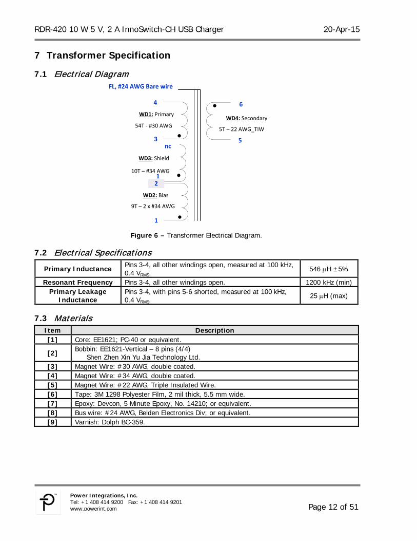
Transformer Specification 7
Electrical Diagram 7.1
Figure 6 – Transformer Electrical Diagram.
Electrical Specifications 7.2
Primary Inductance Pins 3-4, all other windings open, measured at 100 kHz, 0.4 VRMS.
546 µH ±5%
Resonant Frequency Pins 3-4, all other windings open. 1200 kHz (min) Primary Leakage
Inductance Pins 3-4, with pins 5-6 shorted, measured at 100 kHz, 0.4 VRMS.
25 µH (max)
Materials 7.3Item Description [1] Core: EE1621; PC-40 or equivalent.
[2] Bobbin: EE1621-Vertical – 8 pins (4/4) Shen Zhen Xin Yu Jia Technology Ltd.
[3] Magnet Wire: #30 AWG, double coated. [4] Magnet Wire: #34 AWG, double coated. [5] Magnet Wire: #22 AWG, Triple Insulated Wire. [6] Tape: 3M 1298 Polyester Film, 2 mil thick, 5.5 mm wide. [7] Epoxy: Devcon, 5 Minute Epoxy, No. 14210; or equivalent. [8] Bus wire: #24 AWG, Belden Electronics Div; or equivalent. [9] Varnish: Dolph BC-359.
3
4
1
2
WD1: Primary
54T - #30 AWG
nc
WD2: Bias
9T – 2 x #34 AWG
WD3: Shield
10T – #34 AWG
WD4: Secondary
5T – 22 AWG_TIW
6
5
FL, #24 AWG Bare wire
1

20-Apr-15 RDR-420 10 W 5 V, 2 A InnoSwitch-CH USB Charger
Page 13 of 51
Power Integrations Tel: +1 408 414 9200 Fax: +1 408 414
9201
Transformer Build Diagram 7.4
Figure 7 – Transformer Build Diagram.
Transformer Instructions 7.5
Winding Preparation
For the purpose of these instructions, bobbin is oriented on winder such that pin side is on the left side. Winding direction is clockwise direction.
WD1 Primary
Start at pin 3, wind 54 turns wire item [2] in 3 layers (18T/layer) with tight tension. At the last turn bring the wire back to the left and finish at pin 4.
Insulation 1 layer of tape [6] for insulation.
WD2 & WD3 Bias & Shield
Use 3 wires item [4], start at pin 1, and wind 9 turns from left to right. At the last turn, bring 2 wires to the left to terminate at pin 2 for WD2. Then continue winding on the 3rd wire 1 more turn and left no-connect for WD3.
Insulation 1 layer of tape [6] for insulation. WD4
Secondary Start at pin 6, wind 5 turns wire item [5], spread wire evenly. At the last turn bring the wire back to the left and finish at pin 5.
Insulation 2 Layer of tape [6] to secure the windings.
Finish
Gap core halves for 546 µH inductance. Place epoxy item [7] onto both center legs of core halves, (see illustration below). Wrap core halves and bus wire item [8] with tape, (see illustration below). Varnish with item [9].
3
4
12
NC
5
6
WD1: Primary 54T - #30 AWG
WD2: Bias 9T – 2x#34 AWG
WD3: Shield 10T – #34 AWG(wound in parallel with…)
WD4: Secondary5T – #22 AWG_TIW

RDR-420 10 W 5 V, 2 A InnoSwitch-CH USB Charger 20-Apr-15
Page 14 of 51
Power Integrations, Inc. Tel: +1 408 414 9200 Fax: +1 408 414 9201 www.powerint.com
Transformer I llustrations 7.6
Winding Preparation
For the purpose of these instructions, bobbin is oriented on winder such that pin side is on the left side. Winding direction is clockwise direction.
WD1 Primary
Start at pin 3, wind 54 turns wire item [2] in 3 layers (18T/layer) with tight tension. At the last turn bring the wire back to the left and finish at pin 4.

20-Apr-15 RDR-420 10 W 5 V, 2 A InnoSwitch-CH USB Charger
Page 15 of 51
Power Integrations Tel: +1 408 414 9200 Fax: +1 408 414
9201
Insulation
1 layer of tape [6] for insulation.
WD2 & WD3 Bias & Shield
Use 3 wires item [4], start at pin 1, and wind 9 turns from left to right. At the last turn, bring 2 wires to the left to terminate at pin 2 for WD2. Then continue winding on the 3rd wire 1 more turn and left no-connect for WD3.
2 wires for WD2

RDR-420 10 W 5 V, 2 A InnoSwitch-CH USB Charger 20-Apr-15
Page 16 of 51
Power Integrations, Inc. Tel: +1 408 414 9200 Fax: +1 408 414 9201 www.powerint.com
Insulation
1 layer of tape [6] for insulation.
WD4 Secondary
Start at pin 6, wind 5 turns wire item [5], spread wire evenly. At the last turn bring the wire back to the left and finish at pin 5.
Insulation
2 layer of tape [6] to secure the windings.
3rd wire left NC for WD3

20-Apr-15 RDR-420 10 W 5 V, 2 A InnoSwitch-CH USB Charger
Page 17 of 51
Power Integrations Tel: +1 408 414 9200 Fax: +1 408 414
9201
Finish
Gap core halves for 546 µH inductance. Place epoxy item [7] onto both center legs of core halves, (see illustration beside). Wrap core halves and bus wire item [8] with tape, (see illustration below). Varnish with item [9].
bus wire item [8] left ~ 40 mm floating on primary side
RDR-420 10 W 5 V, 2 A InnoSwitch-CH USB Charger 20-Apr-15
Page 18 of 51
Power Integrations, Inc. Tel: +1 408 414 9200 Fax: +1 408 414 9201 www.powerint.com
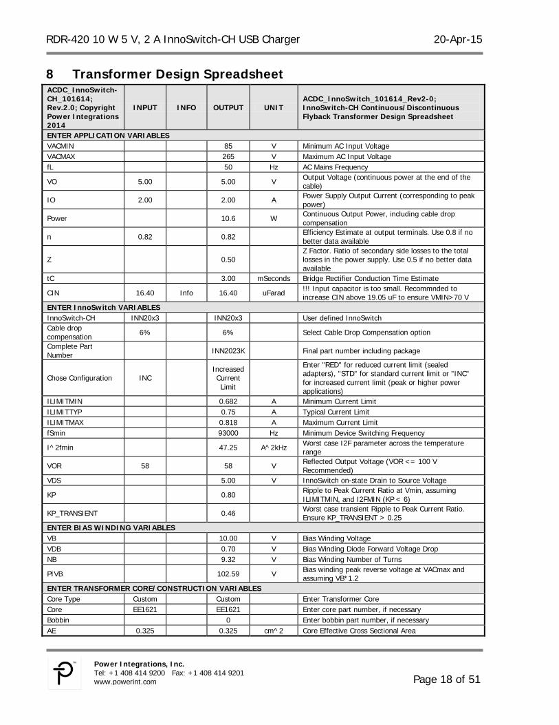
Transformer Design Spreadsheet 8ACDC_InnoSwitch-CH_101614; Rev.2.0; Copyright Power Integrations 2014
INPUT INFO OUTPUT UNIT ACDC_InnoSwitch_101614_Rev2-0; InnoSwitch-CH Continuous/Discontinuous Flyback Transformer Design Spreadsheet
ENTER APPLICATION VARIABLES VACMIN 85 V Minimum AC Input Voltage VACMAX 265 V Maximum AC Input Voltage fL 50 Hz AC Mains Frequency
VO 5.00 5.00 V Output Voltage (continuous power at the end of the cable)
IO 2.00 2.00 A Power Supply Output Current (corresponding to peak power)
Power 10.6 W Continuous Output Power, including cable drop compensation
n 0.82 0.82 Efficiency Estimate at output terminals. Use 0.8 if no better data available
Z 0.50
Z Factor. Ratio of secondary side losses to the total losses in the power supply. Use 0.5 if no better data available
tC 3.00 mSeconds Bridge Rectifier Conduction Time Estimate
CIN 16.40 Info 16.40 uFarad !!! Input capacitor is too small. Recommnded to increase CIN above 19.05 uF to ensure VMIN>70 V
ENTER InnoSwitch VARIABLES InnoSwitch-CH INN20x3 INN20x3 User defined InnoSwitch Cable drop compensation 6% 6% Select Cable Drop Compensation option
Complete Part Number INN2023K Final part number including package
Chose Configuration INC
Increased Current Limit
Enter "RED" for reduced current limit (sealed adapters), "STD" for standard current limit or "INC" for increased current limit (peak or higher power applications)
ILIMITMIN 0.682 A Minimum Current Limit ILIMITTYP 0.75 A Typical Current Limit ILIMITMAX 0.818 A Maximum Current Limit fSmin 93000 Hz Minimum Device Switching Frequency
I^2fmin 47.25 A^2kHz Worst case I2F parameter across the temperature range
VOR 58 58 V Reflected Output Voltage (VOR <= 100 V Recommended)
VDS 5.00 V InnoSwitch on-state Drain to Source Voltage
KP 0.80 Ripple to Peak Current Ratio at Vmin, assuming ILIMITMIN, and I2FMIN (KP < 6)
KP_TRANSIENT 0.46 Worst case transient Ripple to Peak Current Ratio. Ensure KP_TRANSIENT > 0.25
ENTER BIAS WINDING VARIABLES VB 10.00 V Bias Winding Voltage VDB 0.70 V Bias Winding Diode Forward Voltage Drop NB 9.32 V Bias Winding Number of Turns
PIVB 102.59 V Bias winding peak reverse voltage at VACmax and assuming VB*1.2
ENTER TRANSFORMER CORE/CONSTRUCTION VARIABLES Core Type Custom Custom Enter Transformer Core Core EE1621 EE1621 Enter core part number, if necessary Bobbin 0 Enter bobbin part number, if necessary AE 0.325 0.325 cm^2 Core Effective Cross Sectional Area

20-Apr-15 RDR-420 10 W 5 V, 2 A InnoSwitch-CH USB Charger
Page 19 of 51
Power Integrations Tel: +1 408 414 9200 Fax: +1 408 414
9201
LE 3.93 3.93 cm Core Effective Path Length AL 2800 2800 nH/T^2 Ungapped Core Effective Inductance BW 5.40 5.40 mm Bobbin Physical Winding Width
M 0.00 mm Safety Margin Width (Half the Primary to Secondary Creepage Distance)
L 3 3 Number of Primary Layers NS 5 5 Number of Secondary Turns DC INPUT VOLTAGE PARAMETERS
VMIN 62 Warning 62 V !!! Minimum DC Input Voltage < 70 Volts. Increase VACMIN or increase CIN
VMAX 375 V Maximum DC Input Voltage CURRENT WAVEFORM SHAPE PARAMETERS
DMAX 0.50 Duty Ratio at full load, minimum primary inductance and minimum input voltage
IAVG 0.21 A Average Primary Current IP 0.682 A Peak Primary Current assuming ILIMITMIN
IR 0.546 A Primary Ripple Current assuming ILIMITMIN, and LPMIN
IRMS 0.31 A Primary RMS Current, assuming ILIMITMIN, and LPMIN
TRANSFORMER PRIMARY DESIGN PARAMETERS
LP 546 uHenry Typical Primary Inductance. +/- 5% to ensure a minimum primary inductance of 518 uH
LP_TOLERANCE 5.0 5.0 % Primary inductance tolerance NP 54 Primary Winding Number of Turns ALG 187 nH/T^2 Gapped Core Effective Inductance
BM 2868 Gauss Maximum Operating Flux Density, BM<3000 is recommended
BAC 1147 Gauss AC Flux Density for Core Loss Curves (0.5 X Peak to Peak)
ur 2694 Relative Permeability of Ungapped Core LG 0.20 mm Gap Length (Lg > 0.1 mm) BWE 16.2 mm Effective Bobbin Width OD 0.30 mm Maximum Primary Wire Diameter including insulation
INS 0.05 mm Estimated Total Insulation Thickness (= 2 * film thickness)
DIA 0.25 mm Bare conductor diameter
AWG 31 AWG Primary Wire Gauge (Rounded to next smaller standard AWG value)
CM 81 Cmils Bare conductor effective area in circular mils
CMA 259 Cmils/Amp Primary Winding Current Capacity (200 < CMA < 500)
TRANSFORMER SECONDARY DESIGN PARAMETERS Lumped parameters ISP 7.37 A Peak Secondary Current, assuming ILIMITMIN ISRMS 3.33 A Secondary RMS Current IRIPPLE 2.67 A Output Capacitor RMS Ripple Current CMS 667 Cmils Secondary Bare Conductor minimum circular mils
AWGS 21 AWG Secondary Wire Gauge (Rounded up to next larger standard AWG value)
VOLTAGE STRESS PARAMETERS VDRAIN 517 V Maximum Drain Voltage Estimate
PIVS 54 V Output Rectifier Maximum Peak Inverse Voltage, assuming the primary has a Voltage spike 40% above VMAX and VO*1.05
TRANSFORMER SECONDARY DESIGN PARAMETERS 1st output VO1 5.30 V Main Output Voltage directly after output rectifier

RDR-420 10 W 5 V, 2 A InnoSwitch-CH USB Charger 20-Apr-15
Page 20 of 51
Power Integrations, Inc. Tel: +1 408 414 9200 Fax: +1 408 414 9201 www.powerint.com
IO1 2.00 A Output DC Current PO1 10.60 W Output Power
VD1 0.06 V Output Synchronous Rectification FET Forward Voltage Drop
NS1 5.00 Turns Output Winding Number of Turns ISRMS1 3.33 A Output Winding RMS Current IRIPPLE1 2.67 A Output Capacitor RMS Ripple Current
PIVS1 54 V Output Rectifier Maximum Peak Inverse Voltage, assuming the primary has a Voltage spike 40% above VMAX and VO*1.05
Recommended MOSFET QM6006 Recommended SR FET for this output
RDSON_HOT 0.027 Ohm RDSon at 100C VRATED 60 V Rated voltage of selected SR FET CMS1 667 Cmils Output Winding Bare Conductor minimum circular mils
AWGS1 21 AWG Wire Gauge (Rounded up to next larger standard AWG value)
DIAS1 0.73 mm Minimum Bare Conductor Diameter ODS1 1.08 mm Maximum Outside Diameter for Triple Insulated Wire

20-Apr-15 RDR-420 10 W 5 V, 2 A InnoSwitch-CH USB Charger
Page 21 of 51
Power Integrations Tel: +1 408 414 9200 Fax: +1 408 414
9201
Performance Data 9All measurements performed with external room ambient temperature and 60 Hz input for 115 VAC range and 50 Hz for 230 VAC input range.
Active Mode Efficiency (at USB Socket) vs. Line 9.1
Figure 8 – Efficiency vs Line Voltage, Room Temperature
80
81
82
83
84
85
86
87
70 90 110 130 150 170 190 210 230 250 270 290
Effic
ienc
y (%
)
Input Voltage (VAC)
RDR-420 10 W 5 V, 2 A InnoSwitch-CH USB Charger 20-Apr-15
Page 22 of 51
Power Integrations, Inc. Tel: +1 408 414 9200 Fax: +1 408 414 9201 www.powerint.com
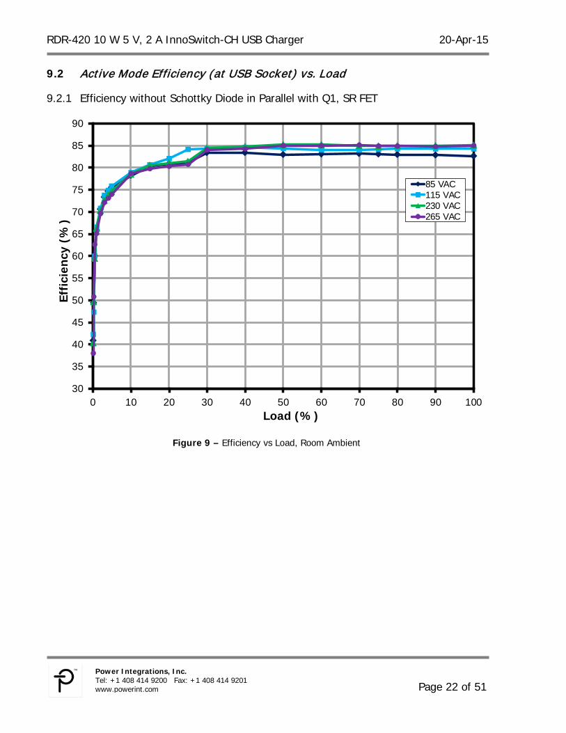
Active Mode Efficiency (at USB Socket) vs. Load 9.2
Efficiency without Schottky Diode in Parallel with Q1, SR FET 9.2.1
Figure 9 – Efficiency vs Load, Room Ambient
30
35
40
45
50
55
60
65
70
75
80
85
90
0 10 20 30 40 50 60 70 80 90 100
Effi
cien
cy (
%)
Load (%)
85 VAC115 VAC230 VAC265 VAC

20-Apr-15 RDR-420 10 W 5 V, 2 A InnoSwitch-CH USB Charger
Page 23 of 51
Power Integrations Tel: +1 408 414 9200 Fax: +1 408 414
9201
Figure 10 - Efficiency vs Load (log scale to demonstrate light load performance)
30
35
40
45
50
55
60
65
70
75
80
85
90
0.1 1.0 10.0 100.0
Effi
cien
cy (
%)
Load (%)
85 VAC115 VAC230 VAC265 VAC

RDR-420 10 W 5 V, 2 A InnoSwitch-CH USB Charger 20-Apr-15
Page 24 of 51
Power Integrations, Inc. Tel: +1 408 414 9200 Fax: +1 408 414 9201 www.powerint.com
Efficiency with a Schottky Diode, SS16, in Parallel with Q1, SR FET 9.2.2
Figure 11 – Efficiency vs Load, Room Temperature, 60 Hz.
35
40
45
50
55
60
65
70
75
80
85
90
0 10 20 30 40 50 60 70 80 90 100
Effi
cien
cy (
%)
Load (%)
85 VAC115 VAC230 VAC265 VAC
20-Apr-15 RDR-420 10 W 5 V, 2 A InnoSwitch-CH USB Charger
Page 25 of 51
Power Integrations Tel: +1 408 414 9200 Fax: +1 408 414
9201
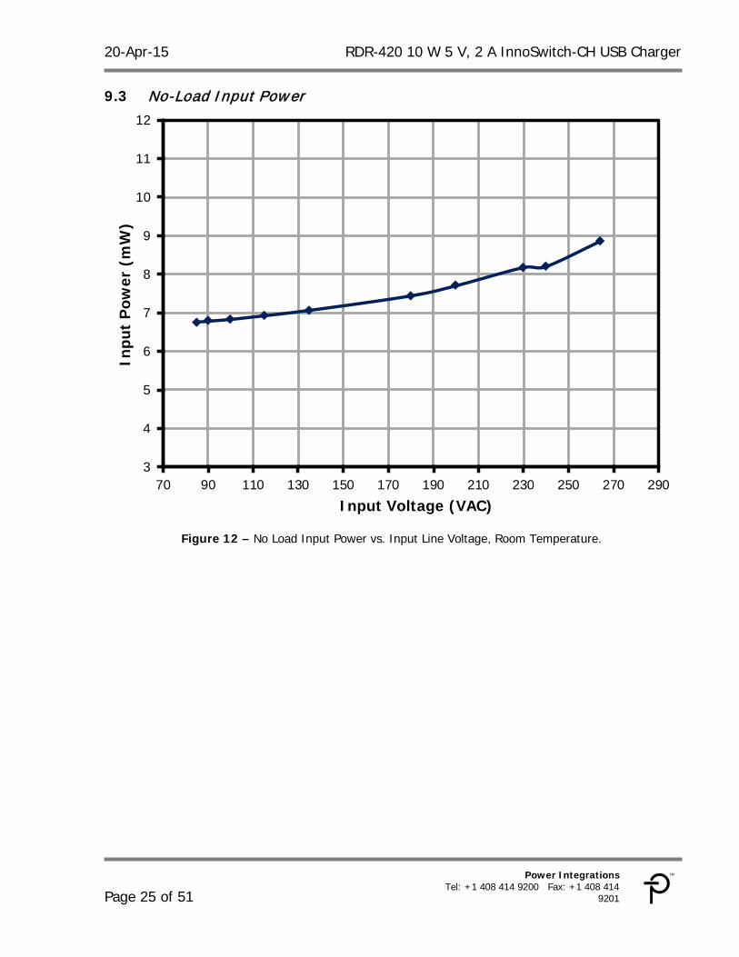
No-Load Input Power 9.3
Figure 12 – No Load Input Power vs. Input Line Voltage, Room Temperature.
3
4
5
6
7
8
9
10
11
12
70 90 110 130 150 170 190 210 230 250 270 290
Inpu
t P
ower
(m
W)
Input Voltage (VAC)
RDR-420 10 W 5 V, 2 A InnoSwitch-CH USB Charger 20-Apr-15
Page 26 of 51
Power Integrations, Inc. Tel: +1 408 414 9200 Fax: +1 408 414 9201 www.powerint.com
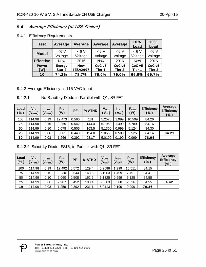
Average Efficiency (at USB Socket) 9.4
Efficiency Requirements 9.4.1
Test Average Average Average Average 10% Load
10% Load
Model <6 V Voltage
<6 V Voltage
<6 V Voltage
<6 V Voltage
<6 V Voltage
<6 V Voltage
Effective Now 2016 Now 2016 Now 2016 Power
[W] Energy Star 2
New IESA2007
CoC v5 Tier 1
CoC v5 Tier 2
CoC v5 Tier 1
CoC v5 Tier 2
10 74.2% 78.7% 76.0% 79.0% 66.6% 69.7%
Average Efficiency at 115 VAC Input 9.4.2
9.4.2.1 No Schottky Diode in Parallel with Q1, SR FET
Load (%)
VIN (VRMS)
IIN (ARMS)
PIN (W) PF %ATHD VOUT
(VDC) IOUT
(ADC) POUT (W)
Efficiency (%)
Average Efficiency
(%) 100 114.98 0.19 12.473 0.566 131 5.2575 1.999 10.509 84.26 75 114.98 0.15 9.255 0.542 144.4 5.1950 1.499 7.789 84.16 50 114.99 0.10 6.078 0.505 163.5 5.1300 0.999 5.124 84.30 25 114.99 0.06 3.001 0.449 194.8 5.0550 0.500 2.525 84.14 84.21 10 114.99 0.03 1.266 0.392 231.7 5.0100 0.199 0.999 78.94
9.4.2.2 Schottky Diode, SS16, in Parallel with Q1, SR FET
Load (%)
VIN (VRMS)
IIN (ARMS)
PIN (W) PF %ATHD VOUT
(VDC) IOUT
(ADC) POUT (W)
Efficiency (%)
Average Efficiency
(%) 100 114.98 0.19 12.492 0.572 129.4 5.2588 1.999 10.511 84.15 75 114.99 0.15 9.230 0.544 143.5 5.1963 1.499 7.791 84.41 50 114.99 0.10 6.060 0.508 162.6 5.1325 0.999 5.125 84.58 25 114.99 0.06 2.987 0.452 193.4 5.0563 0.500 2.526 84.55 84.42 10 114.99 0.03 1.259 0.392 231.1 5.0113 0.199 0.999 79.36

20-Apr-15 RDR-420 10 W 5 V, 2 A InnoSwitch-CH USB Charger
Page 27 of 51
Power Integrations Tel: +1 408 414 9200 Fax: +1 408 414
9201
Average Efficiency at 230 VAC Input 9.4.3
9.4.3.1 No Schottky Diode in Parallel with Q1, SR FET
Load (%)
VIN (VRMS)
IIN (ARMS)
PIN (W) PF %ATHD VOUT
(VDC) IOUT
(ADC) POUT
(W) Efficiency
(%)
Average Efficiency
(%) 100 230.04 0.12 12.364 0.450 195.1 5.2663 1.999 10.527 85.14 75 230.04 0.09 9.179 0.426 209.4 5.2000 1.499 7.797 84.94 50 230.04 0.07 6.021 0.397 228.4 5.1363 0.999 5.130 85.20 25 230.04 0.04 3.097 0.358 258.7 5.0488 0.500 2.522 81.43 84.18 10 230.04 0.02 1.273 0.312 300.9 5.0150 0.199 1.000 78.56
9.4.3.2 Schottky Diode, SS16, in Parallel with Q1, SR FET
Load (%)
VIN (VRMS)
IIN (ARMS)
PIN (W) PF %ATHD VOUT
(VDC) IOUT
(ADC) POUT (W)
Efficiency (%)
Average Efficiency
(%) 100 230.04 0.12 12.329 0.449 195.6 5.2663 1.999 10.527 85.38 75 230.04 0.09 9.133 0.425 210 5.2000 1.499 7.796 85.36 50 230.04 0.07 6.007 0.397 229.2 5.1363 0.999 5.129 85.39 25 230.04 0.04 3.073 0.357 259.5 5.0488 0.500 2.522 82.06 84.55 10 230.04 0.02 1.255 0.312 301.7 5.0150 0.199 1.000 79.68

RDR-420 10 W 5 V, 2 A InnoSwitch-CH USB Charger 20-Apr-15
Page 28 of 51
Power Integrations, Inc. Tel: +1 408 414 9200 Fax: +1 408 414 9201 www.powerint.com
CV/ CC Regulation Measured at the End of Cable 9.5
Figure 13 – Output Voltage vs, Output current, Room Temperature.
0.0
1.0
2.0
3.0
4.0
5.0
6.0
0.0 0.5 1.0 1.5 2.0 2.5
Out
put
Vol
tage
(V
)
Output Current (A)
85 VAC110 VAC230 VAC265 VAC

20-Apr-15 RDR-420 10 W 5 V, 2 A InnoSwitch-CH USB Charger
Page 29 of 51
Power Integrations Tel: +1 408 414 9200 Fax: +1 408 414
9201
Open Case Thermal Performance 10Room ambient.
Figure 14 – Transformer Side.
85 VAC, 2 A Load. Ambient = 26.3 ºC.
Figure 15 – InnoSwitch-CH Side. 85 VAC, 2 A Load. Ambient = 27 ºC.
Figure 16 – Transformer Side. 110 VAC, 2 A Load. Ambient = 26.2 ºC.
Figure 17 – InnoSwitch-CH Side. 110 VAC, 2 A Load. Ambient = 25 ºC.

RDR-420 10 W 5 V, 2 A InnoSwitch-CH USB Charger 20-Apr-15
Page 30 of 51
Power Integrations, Inc. Tel: +1 408 414 9200 Fax: +1 408 414 9201 www.powerint.com
Figure 18 – Transformer Side.
230 VAC, 2 A Load. Ambient = 26.5 ºC.
Figure 19 – InnoSwitch-CH Side. 230 VAC, 2 A Load. Ambient = 25.4 ºC.
Figure 20 – Transformer Side.
265 VAC, 2 A Load. Ambient = 26.5 ºC.
Figure 21 – InnoSwitch-CH Side. 265 VAC, 2 A Load. Ambient = 25.3 ºC.

20-Apr-15 RDR-420 10 W 5 V, 2 A InnoSwitch-CH USB Charger
Page 31 of 51
Power Integrations Tel: +1 408 414 9200 Fax: +1 408 414
9201
Waveforms 11
Load Transient Response (end of cable) 11.1Results were measured with 47 µF at end of cable which is the typical specified measurement condition for mobile phone chargers.
Figure 22 – Transient Response (4.5 VMIN). 85 VAC, 0-2 A Load Step. Upper: ILOAD, 1 A / div. Lower: VOUT, 500 mV, 50 ms / div.
Figure 23 – Transient Response (4.5 VMIN). 110 VAC, 0-2 A Load Step. Upper: ILOAD, 1 A / div. Lower: VOUT, 500 mV, 50 ms / div.
Figure 24 – Transient Response (4.6 VMIN).
230 VAC, 0-2 A Load Step. Upper: ILOAD, 1 A / div. Lower: VOUT, 500 mV, 50 ms / div.
Figure 25 – Transient Response (4.6 VMIN). 265 VAC, 0-2 A Load Step. Upper: ILOAD, 1 A / div. Lower: VOUT, 500 mV, 50 ms / div.

RDR-420 10 W 5 V, 2 A InnoSwitch-CH USB Charger 20-Apr-15
Page 32 of 51
Power Integrations, Inc. Tel: +1 408 414 9200 Fax: +1 408 414 9201 www.powerint.com
Load Transient Response (at USB Socket) 11.2
Figure 26 – Transient Response (4.75 VMIN). 85 VAC, 0-2 A Load Step. Upper: ILOAD, 1 A / div. Lower: VOUT, 500 mV, 50 ms / div.
Figure 27 – Transient Response (4.75 VMIN). 110 VAC, 0-2 A Load Step. Upper: ILOAD, 1 A / div. Lower: VOUT, 500 mV, 50 ms / div.
Figure 28 – Transient Response (4.85 VMIN).
230 VAC, 0-2 A Load Step. Upper: ILOAD, 1 A / div. Lower: VOUT, 500 mV, 50 ms / div.
Figure 29 – Transient Response (4.86 VMIN). 265 VAC, 0-2 A Load Step. Upper: ILOAD, 1 A /div. Lower: VOUT, 500 mV, 50 ms / div.
20-Apr-15 RDR-420 10 W 5 V, 2 A InnoSwitch-CH USB Charger
Page 33 of 51
Power Integrations Tel: +1 408 414 9200 Fax: +1 408 414
9201
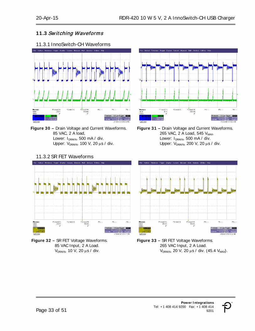
Sw itching Waveforms 11.3
InnoSwitch-CH Waveforms 11.3.1
Figure 30 – Drain Voltage and Current Waveforms.
85 VAC, 2 A load, Lower: IDRAIN, 500 mA / div. Upper: VDRAIN, 100 V, 20 µs / div.
Figure 31 – Drain Voltage and Current Waveforms. 265 VAC, 2 A Load, 545 VMAX. Lower: IDRAIN, 500 mA / div. Upper: VDRAIN, 200 V, 20 µs / div.
SR FET Waveforms 11.3.2
Figure 32 – SR FET Voltage Waveforms.
85 VAC Input, 2 A Load. VDRAIN, 10 V, 20 µs / div.
Figure 33 – SR FET Voltage Waveforms. 265 VAC Input, 2 A Load. VDRAIN, 20 V, 20 µs / div. (45.4 VMAX).

RDR-420 10 W 5 V, 2 A InnoSwitch-CH USB Charger 20-Apr-15
Page 34 of 51
Power Integrations, Inc. Tel: +1 408 414 9200 Fax: +1 408 414 9201 www.powerint.com
Output Ripple Measurements 11.4
Ripple Measurement Technique 11.4.1For DC output ripple measurements, a modified oscilloscope test probe must be utilized in order to reduce spurious signals due to pick-up. Details of the probe modification are provided in the Figures below. The 4987BA probe adapter is affixed with two capacitors tied in parallel across the probe tip. The capacitors include one (1) 0.1 µF/50 V ceramic type and one (1) 47 µF/50 V aluminum electrolytic. The aluminum electrolytic type capacitor is polarized, so proper polarity across DC outputs must be maintained (see below).
Figure 34 – Oscilloscope Probe Prepared for Ripple Measurement. (End Cap and Ground Lead Removed)
Figure 35 – Oscilloscope Probe with Probe Master (www.probemaster.com) 4987A BNC Adapter. (Modified with wires for ripple measurement, and two parallel decoupling capacitors added)
Probe Ground
Probe Tip

20-Apr-15 RDR-420 10 W 5 V, 2 A InnoSwitch-CH USB Charger
Page 35 of 51
Power Integrations Tel: +1 408 414 9200 Fax: +1 408 414
9201
Measurement Results 11.4.2Measured at the end of cable.
Figure 36 – Output Ripple Voltage.
85 V RIPPLE (VPK-PK)
115 V RIPPLE (VPK-PK)
230 V RIPPLE (VPK-PK)
265 V RIPPLE (VPK-PK)
0.126 0.123 0.123 0.121
0.00
0.02
0.04
0.06
0.08
0.10
0.12
0.14
0.0 0.2 0.4 0.6 0.8 1.0 1.2 1.4 1.6 1.8 2.0
Rip
ple
(mV
PK
-PK
)
Current (mA)
85 V115 V230 V265 V

RDR-420 10 W 5 V, 2 A InnoSwitch-CH USB Charger 20-Apr-15
Page 36 of 51
Power Integrations, Inc. Tel: +1 408 414 9200 Fax: +1 408 414 9201 www.powerint.com
Conductive EMI 12
2 A Resistive Load, Floating Output (PK / AV) 12.1After running 5 minutes.
Freq (MHz) QP Limit Margin 0.19 50.48 63.95 13.47
Figure 37 – Floating Ground EMI at 115 VAC.

20-Apr-15 RDR-420 10 W 5 V, 2 A InnoSwitch-CH USB Charger
Page 37 of 51
Power Integrations Tel: +1 408 414 9200 Fax: +1 408 414
9201
Figure 38 – Floating Ground at 230 VAC.

RDR-420 10 W 5 V, 2 A InnoSwitch-CH USB Charger 20-Apr-15
Page 38 of 51
Power Integrations, Inc. Tel: +1 408 414 9200 Fax: +1 408 414 9201 www.powerint.com
2 A Resistive Load, Artificial Hand Ground (PK / AV) 12.2
FREQ (MHZ) QP LIMIT MARGIN
0.20 52.26 63.82 11.56 1.37 44.97 56 11.03 1.73 41.65 56 14.35
Figure 39 – Artificial Ground at 115 VAC.

20-Apr-15 RDR-420 10 W 5 V, 2 A InnoSwitch-CH USB Charger
Page 39 of 51
Power Integrations Tel: +1 408 414 9200 Fax: +1 408 414
9201
FREQ (MHZ) QP LIMIT MARGIN
0.50 43.6 56.07 12.47 0.99 47.3 56 8.7 1.62 44.51 56 11.49 4.65 41.37 56 14.63
Figure 40 – Artificial Ground at 230 VAC.

RDR-420 10 W 5 V, 2 A InnoSwitch-CH USB Charger 20-Apr-15
Page 40 of 51
Power Integrations, Inc. Tel: +1 408 414 9200 Fax: +1 408 414 9201 www.powerint.com
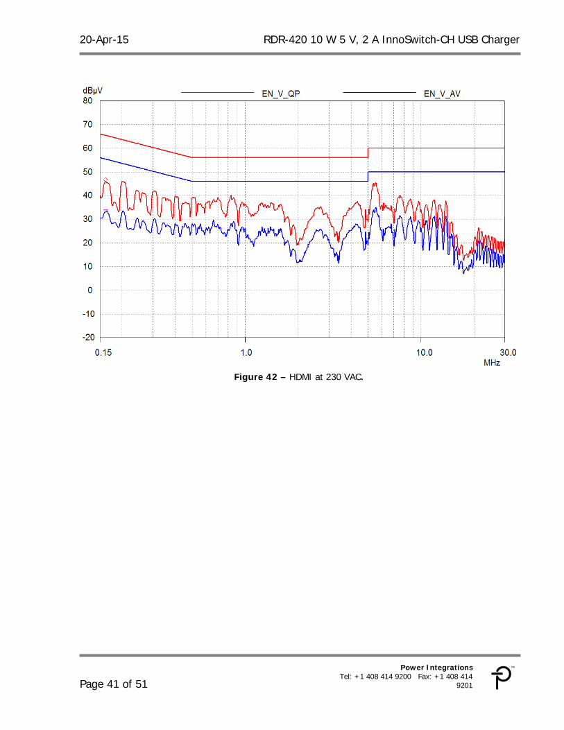
Smartphone w ith Monitor Set-up (HDMI) (QP / AV) 12.3 Phone is connected to charger and LCD monitor. The monitor connection increases capacitance to earth ground.
Figure 41 – HDMI at 115 VAC.
20-Apr-15 RDR-420 10 W 5 V, 2 A InnoSwitch-CH USB Charger
Page 41 of 51
Power Integrations Tel: +1 408 414 9200 Fax: +1 408 414
9201
Figure 42 – HDMI at 230 VAC.

RDR-420 10 W 5 V, 2 A InnoSwitch-CH USB Charger 20-Apr-15
Page 42 of 51
Power Integrations, Inc. Tel: +1 408 414 9200 Fax: +1 408 414 9201 www.powerint.com
Radiative EMI 13
Figure 43 – Radiation at 110 VAC.
Maximized quasi-peak readings (NO manipulation of EUT interface cables)Frequency Level Pol Detector Azimuth Height Comments
MHz dBµV/m v/h Limit Margin Pk/QP/Avg degrees meters30.234 23.7 V 30.0 -6.3 QP 4 1.0 QP (1.00s)
185.989 19.4 H 30.0 -10.6 QP 116 4.0 QP (1.00s)
Class B

20-Apr-15 RDR-420 10 W 5 V, 2 A InnoSwitch-CH USB Charger
Page 43 of 51
Power Integrations Tel: +1 408 414 9200 Fax: +1 408 414
9201
Figure 44 – Radiation at 230 VAC.
Maximized quasi-peak readings (NO manipulation of EUT interface cables)Frequency Level Pol Detector Azimuth Height Comments
MHz dBµV/m v/h Limit Margin Pk/QP/Avg degrees meters30.287 23.8 V 30.0 -6.2 QP 57 1.0 QP (1.00s)
191.605 19.9 H 30.0 -10.1 QP 121 4.0 QP (1.00s)
Class B

RDR-420 10 W 5 V, 2 A InnoSwitch-CH USB Charger 20-Apr-15
Page 44 of 51
Power Integrations, Inc. Tel: +1 408 414 9200 Fax: +1 408 414 9201 www.powerint.com
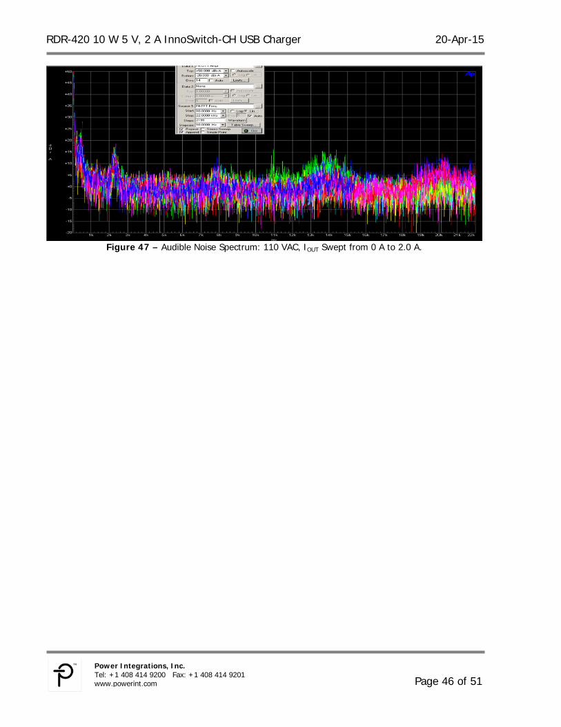
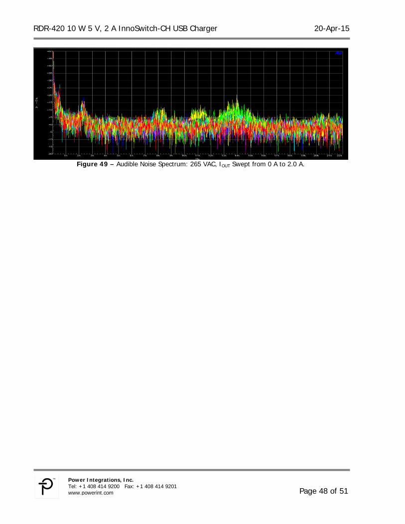
Audible Noise 14Test performed inside case with microphone placed 3 mm from case surface on long side of case, transformer facing towards microphone.
Figure 45 – Audible Noise Spectrum: No-load, VIN Swept from 85 VAC to 264 VAC.

20-Apr-15 RDR-420 10 W 5 V, 2 A InnoSwitch-CH USB Charger
Page 45 of 51
Power Integrations Tel: +1 408 414 9200 Fax: +1 408 414
9201
Figure 46 – Audible Noise Spectrum: 85 VAC, IOUT Swept from 0 A to 2.0 A.
RDR-420 10 W 5 V, 2 A InnoSwitch-CH USB Charger 20-Apr-15
Page 46 of 51
Power Integrations, Inc. Tel: +1 408 414 9200 Fax: +1 408 414 9201 www.powerint.com
Figure 47 – Audible Noise Spectrum: 110 VAC, IOUT Swept from 0 A to 2.0 A.

20-Apr-15 RDR-420 10 W 5 V, 2 A InnoSwitch-CH USB Charger
Page 47 of 51
Power Integrations Tel: +1 408 414 9200 Fax: +1 408 414
9201
Figure 48 – Audible Noise Spectrum: 220 VAC, IOUT Swept from 0 A to 2.0A.
RDR-420 10 W 5 V, 2 A InnoSwitch-CH USB Charger 20-Apr-15
Page 48 of 51
Power Integrations, Inc. Tel: +1 408 414 9200 Fax: +1 408 414 9201 www.powerint.com
Figure 49 – Audible Noise Spectrum: 265 VAC, IOUT Swept from 0 A to 2.0 A.

20-Apr-15 RDR-420 10 W 5 V, 2 A InnoSwitch-CH USB Charger
Page 49 of 51
Power Integrations Tel: +1 408 414 9200 Fax: +1 408 414
9201
Lighting Surge & ESD Test 15
Differential Mode Test 15.1Passed ±1 kV, 500 A surge test
Common Mode Test 15.2Passed ±6 KV, 500 A ring wave test. Need to install plastic barrier for >5 kV ring wave common mode surge test.
ESD Test 15.3Passed ±16.5 kV air, 8 kV contact. Need to install plastic barrier to pass ESD test.

RDR-420 10 W 5 V, 2 A InnoSwitch-CH USB Charger 20-Apr-15
Page 50 of 51
Power Integrations, Inc. Tel: +1 408 414 9200 Fax: +1 408 414 9201 www.powerint.com
Revision History 16Date Author Revision Description & Changes Reviewed 11-Nov-14 DK 1.0 Initial Release Mktg & Apps 20-Apr-15 KM 1.1 Updated Transformer Resonant
Frequency Spec, CV/CC Graph and Output Ripple Table

20-Apr-15 RDR-420 10 W 5 V, 2 A InnoSwitch-CH USB Charger
Page 51 of 51
Power Integrations Tel: +1 408 414 9200 Fax: +1 408 414
9201
For the latest updates, visit our website: www.power.com Power Integrations reserves the right to make changes to its products at any time to improve reliability or manufacturability. Power Integrations does not assume any liability arising from the use of any device or circuit described herein. POWER INTEGRATIONS MAKES NO WARRANTY HEREIN AND SPECIFICALLY DISCLAIMS ALL WARRANTIES INCLUDING, WITHOUT LIMITATION, THE IMPLIED WARRANTIES OF MERCHANTABILITY, FITNESS FOR A PARTICULAR PURPOSE, AND NON-INFRINGEMENT OF THIRD PARTY RIGHTS.
PATENT INFORMATION The products and applications illustrated herein (including transformer construction and circuits’ external to the products) may be covered by one or more U.S. and foreign patents, or potentially by pending U.S. and foreign patent applications assigned to Power Integrations. A complete list of Power Integrations’ patents may be found at www.power.com. Power Integrations grants its customers a license under certain patent rights as set forth at http://www.power.com/ip.htm. The PI Logo, TOPSwitch, TinySwitch, LinkSwitch, LYTSwitch, InnoSwtich, DPA-Switch, PeakSwitch, CAPZero, SENZero, LinkZero, HiperPFS, HiperTFS, HiperLCS, Qspeed, EcoSmart, Clampless, E-Shield, Filterfuse, FluxLink, StackFET, PI Expert and PI FACTS are trademarks of Power Integrations, Inc. Other trademarks are property of their respective companies. ©Copyright 2015 Power Integrations, Inc. Power Integrations Worldwide Sales Support Locations
WORLD HEADQUARTERS 5245 Hellyer Avenue San Jose, CA 95138, USA. Main: +1-408-414-9200 Customer Service: Phone: +1-408-414-9665 Fax: +1-408-414-9765 e-mail: [email protected]
GERMANY Lindwurmstrasse 114 80337, Munich Germany Phone: +49-895-527-39110 Fax: +49-895-527-39200 e-mail: [email protected]
JAPAN Kosei Dai-3 Building 2-12-11, Shin-Yokohama, Kohoku-ku, Yokohama-shi, Kanagawa 222-0033 Japan Phone: +81-45-471-1021 Fax: +81-45-471-3717 e-mail: [email protected]
TAIWAN 5F, No. 318, Nei Hu Rd., Sec. 1 Nei Hu District Taipei 11493, Taiwan R.O.C. Phone: +886-2-2659-4570 Fax: +886-2-2659-4550 e-mail: [email protected]
CHINA (SHANGHAI) Rm 2410, Charity Plaza, No. 88, North Caoxi Road, Shanghai, PRC 200030 Phone: +86-21-6354-6323 Fax: +86-21-6354-6325 e-mail: [email protected]
INDIA #1, 14th Main Road Vasanthanagar Bangalore-560052 India Phone: +91-80-4113-8020 Fax: +91-80-4113-8023 e-mail: [email protected]
KOREA RM 602, 6FL Korea City Air Terminal B/D, 159-6 Samsung-Dong, Kangnam-Gu, Seoul, 135-728 Korea Phone: +82-2-2016-6610 Fax: +82-2-2016-6630 e-mail: [email protected]
UK First Floor, Unit 15, Meadway Court, Rutherford Close, Stevenage, Herts. SG1 2EF United Kingdom Phone: +44 (0) 1252-730-141 Fax: +44 (0) 1252-727-689 e-mail: [email protected]
CHINA (SHENZHEN) 17/F, Hivac Building, No. 2, Keji Nan 8th Road, Nanshan District, Shenzhen, China, 518057 Phone: +86-755-8672-8689 Fax: +86-755-8672-8690 e-mail: [email protected]
ITALY Via Milanese 20, 3rd. Fl. 20099 Sesto San Giovanni (MI) Italy Phone: +39-024-550-8701 Fax: +39-028-928-6009 e-mail: [email protected]
SINGAPORE 51 Newton Road, #19-01/05 Goldhill Plaza Singapore, 308900 Phone: +65-6358-2160 Fax: +65-6358-2015 e-mail: [email protected]