Embed Size (px)
Citation preview
REDUCTION OF SHAFT VOLTAGES AND BEARING CURRENTS IN FIVE-
PHASE INDUCTION MOTORS
A Thesis
by
HUSSAIN A. I. A. HUSSAIN
Submitted to the Office of Graduate Studies of Texas A&M University
in partial fulfillment of the requirements for the degree of
MASTER OF SCIENCE
May 2012
Major Subject: Electrical Engineering

Reduction of Shaft Voltages and Bearing Currents in Five-Phase Induction Motors
Copyright 2012 Hussain A. I. A. Hussain
REDUCTION OF SHAFT VOLTAGES AND BEARING CURRENTS IN FIVE-
PHASE INDUCTION MOTORS
A Thesis
by
HUSSAIN A. I. A. HUSSAIN
Submitted to the Office of Graduate Studies of Texas A&M University
in partial fulfillment of the requirements for the degree of
MASTER OF SCIENCE
Approved by:
Chair of Committee, Hamid A. Toliyat Committee Members, Robert Balog Shankar P. Bhattacharyya Won-jong Kim Head of Department, Costas N. Georghiades
May 2012
Major Subject: Electrical Engineering
iii
ABSTRACT
Reduction of Shaft Voltages and Bearing Currents in Five-Phase Induction Motor.
(May 2012)
Hussain A. I. A. Hussain, B.Sc Electrical Engineering, Kuwait University
Chair of Advisory Committee: Dr. Hamid A. Toliyat
Induction motors are commonly used in numerous industrial applications. To
maintain a reliable operation of the motor, it is important to identify the potential faults
that may cause the motor to fail. Bearing failures are one of the main causes of motor
breakdown. The causes of bearing damage have been studied in detail for a long time. In
some cases, bearing failed due to the current passing through them. In this thesis, bearing
currents in an inverter driven five-phase induction motor are studied and a new solution
is proposed.
First, theory of shaft voltage and bearing current are presented. The causes are
identified and current solutions are discussed. Then, new switching patterns are proposed
for the five-phase induction motor. The new schemes apply a modified algorithm for the
space vector pulse-width-modulation (SVPWM). The system is simulated and the results
of the new switching patterns are compared with the conventional switching pattern.
Finally, the new schemes are experimentally tested using a digital signal processor
(DSP) to drive the five-phase IGBT inverter. The experimental results verified that the

iv
new switching pattern could reduce shaft voltages and bearing current without affecting
the performance.

v
To my family

vi
ACKNOWLEDGEMENTS
I would like to thank Dr. Hamid Toliyat for his continuous help and guidance
throughout the course of the research.
Thanks also go to the members of my graduate study committee for their support.
Also I would also like to thank my colleagues in the Advanced Electric Machines and
Power Electronics (EMPE) Laboratory for their valuable help.
vii
TABLE OF CONTENTS
Page
CHAPTER I INTRODUCTION AND LITERATURE REVIEW................................... 1
1. Introduction ........................................................................................................ 1
2. Shaft voltage generation ..................................................................................... 2 3. Parasitic capacitances inside motors ................................................................... 5
4. Bearing impedance model .................................................................................. 7 5. Solutions to the problem ..................................................................................... 9
CHAPTER II QD0 TRANSFORMATION ................................................................. 11
1. Introduction ...................................................................................................... 11 2. qd0 in three phase machine ............................................................................... 11
3. Expanding qd0 transformation to five-phase system ......................................... 14 4. Properties of the qd0 transformation ................................................................. 17
CHAPTER III FIVE PHASE INDUCTION MOTOR MODEL .................................. 19
1. Voltage, current and flux linkage ...................................................................... 19 2. Resistances and inductances ............................................................................. 21
3. abc equations .................................................................................................... 22 4. qd0 equations ................................................................................................... 24
5. qd0 torque and speed ........................................................................................ 28
CHAPTER IV INVERTER MODEL .......................................................................... 29
1. Introduction ...................................................................................................... 29 2. Five-phase SVPWM ......................................................................................... 33
3. Previously proposed switching patterns ............................................................ 38 4. Choosing switching vectors .............................................................................. 39
5. Implementing 5L6 switching pattern ................................................................ 44 6. 6L Switching pattern ........................................................................................ 47
CHAPTER V ZERO SEQUENCE CIRCUIT .............................................................. 50
1. Introduction ...................................................................................................... 50 2. Step response ................................................................................................... 54
3. Special case ...................................................................................................... 56
viii
CHAPTER VI SIMULATIONS AND EXPERIMENTAL RESULTS ........................ 59
1. Obtaining zero sequence circuit parameters’ values .......................................... 59 2. Simulation results ............................................................................................. 62
3. Experiment setup .............................................................................................. 66 4. Experimental results ......................................................................................... 68
5. Current regulation ............................................................................................ 73 6. Comparing (6L) with (2L+2M) under CRPWM ............................................... 76
CHAPTER VII CONCLUSIONS AND FUTURE WORK .......................................... 79
REFERENCES ............................................................................................................ 80
VITA ........................................................................................................................... 83
ix
LIST OF FIGURES
Page
Fig. 1 : Reasons of bearing damage [1] .......................................................................... 2
Fig. 2 : Fluting the bearing [10] ...................................................................................... 3
Fig. 3 : Motor stator model............................................................................................. 4
Fig. 4 : (a) Sinusoidal three-phase volatge source (b) neutral point voltage ..................... 5
Fig. 5 : PWM volatge source (a) Va (b) Vb (c) Vc (d) neutral point voltage ................... 5
Fig. 6 : Current paths in the mechanical system .............................................................. 6
Fig. 7 : Model of parasitic capacitance in the motor ....................................................... 6
Fig. 8 : (a) Per ball model, (b) Model of bearings ........................................................... 7
Fig. 9 : Final bearing model ........................................................................................... 8
Fig. 10 : abc and qd vectors .......................................................................................... 11
Fig. 11 : stationary qd0 frame....................................................................................... 12
Fig. 12 : abc rotor frame and qd0 frame ....................................................................... 13
Fig. 13 : Five sequences in five-phase system .............................................................. 15
Fig. 14 : q1-d1 and q2-d2 Five Phase System ............................................................... 16
Fig. 15 : Induction motor circuit ................................................................................... 19
Fig. 16 : Motor Drive System ....................................................................................... 29
Fig. 17 : Three phase Inveter ........................................................................................ 30
Fig. 18 : Carrier based PWM (a) command and carrier signals (b) output signal ........... 30
Fig. 19 : Three Phase Space Vector PWM Vectors ....................................................... 32
Fig. 20 : Five Phase Inverter ........................................................................................ 33

x
Fig. 21 : The 32 states represented on q1-d1 and q2-d2. ............................................... 35
Fig. 22 : Vector Numbers in (a) Sector 1 and (b) Sector 2. ........................................... 37
Fig. 23 : (a) Example of achievable range of reference volatge, (b) Maxiumum range of reference voltage. ......................................................................................................... 41
Fig. 24 : (a) 5L5, (b) 5L6, (c) 5L7, (d) 5l8. ................................................................... 42
Fig. 25 : Switching Cycle (Mode 1) ............................................................................. 46
Fig. 26 : Switching Cycle (Mode 2) ............................................................................. 46
Fig. 27 : 6L switching scheme ...................................................................................... 48
Fig. 28 : Motor drive system ........................................................................................ 50
Fig. 29 : Inverter and motor model ............................................................................... 51
Fig. 30 : Zero sequence circuit ..................................................................................... 52
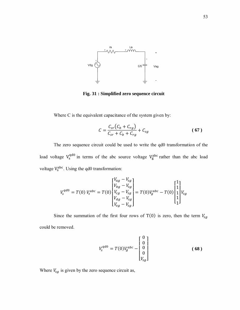
Fig. 31 : Simplified zero sequence circuit ..................................................................... 53
Fig. 32 : Step Response (a) with zero intial condition (b) intial condition = -1 .............. 56
Fig. 33 : Step response, (a) with zero intial condition, (b) intial condition = -1 ............. 57
Fig. 34 : Zero sequence Circuit .................................................................................... 59
Fig. 35 : (2L) Simulation results ................................................................................... 63
Fig. 36 : (2L+2M) Simulation results ........................................................................... 63
Fig. 37 : (4L) Simulation results ................................................................................... 64
Fig. 38 : (5L8) Simulation results ................................................................................. 64
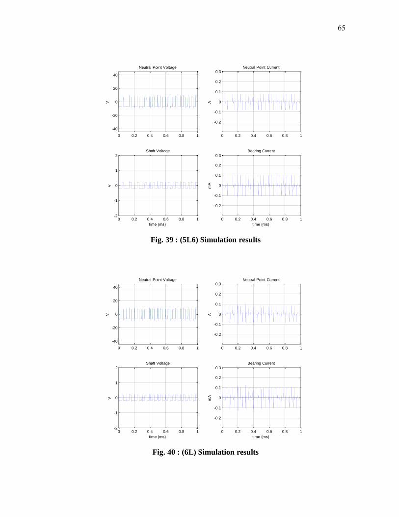
Fig. 39 : (5L6) Simulation results ................................................................................. 65
Fig. 40 : (6L) Simulation results ................................................................................... 65
Fig. 41 : Motor configuration. ...................................................................................... 67
Fig. 42 : Experiment setup ........................................................................................... 68
xi
Fig. 43 : (2L) Experimental results ............................................................................... 69
Fig. 44 : (2L+2M) Experimental results ....................................................................... 70
Fig. 45 : (4L) Experimental results ............................................................................... 70
Fig. 46 : (5L6) Experimental results ............................................................................. 71
Fig. 47 : (5L8) Experimental results ............................................................................. 71
Fig. 48 : (6L) Experimental results ............................................................................... 72
Fig. 49 : Current Regulated SVPWM ........................................................................... 74
Fig. 50 : Stationary and rotating refrence frames. ......................................................... 75
Fig. 51 : 2L+2M Sequence (a) Iq (b) Id (c) Stator Currents (d) Torque (e) Speed ......... 77
Fig. 52 : 6L Sequence (a) Iq (b) Id (c) Stator Currents (d) Torque (e) Speed ................. 78
xii
LIST OF TABLES
Page
Table 1 : States of the three phase inverter ................................................................... 31
Table 2 : States of the five phase inverter ..................................................................... 34
Table 3 : Total harmonic distortion .............................................................................. 38
Table 4 : Number of switchings (5L) ............................................................................ 43
Table 5 : Total harmonic distortion (5L)....................................................................... 43
Table 6 : 5L6 switching pattern for each sector ............................................................ 45
Table 7 : Total harmonic distortion (6L)....................................................................... 48
Table 8 : 6L switching pattern for each sector .............................................................. 49
Table 9 : Parameter values ........................................................................................... 61
Table 10 : THD for various switching scheme (simulation) .......................................... 62
Table 11 : THD and current for various switching scheme (experiments) ..................... 68
1
CHAPTER I
INTRODUCTION AND LITERATURE REVIEW
1. Introduction
For the past century, induction motor was widely used in the industry due to its
simple and robust construction. Since the electric power sources are available as three-
phase sources, induction motors were built as three-phase machines. This was true until
Pulse Width Modulated (PWM) drives were introduced which allowed the use of higher
number phases. In conventional PWM drives, the three-phase voltage ac source is
rectified to a dc bus. Then, an inverter is used to convert the dc bus to a controllable
three-phase ac source.
It is not necessary to invert the DC bus to three phases only; it could be inverted
to a different number of phases (e.g., five phases). This introduced the multiphase
motors which have been studied for a long time.
In any motor, there are two bearings which support the rotating shaft with respect
to the stationary frame. Usually, bearings are considered as the first point of failure in a
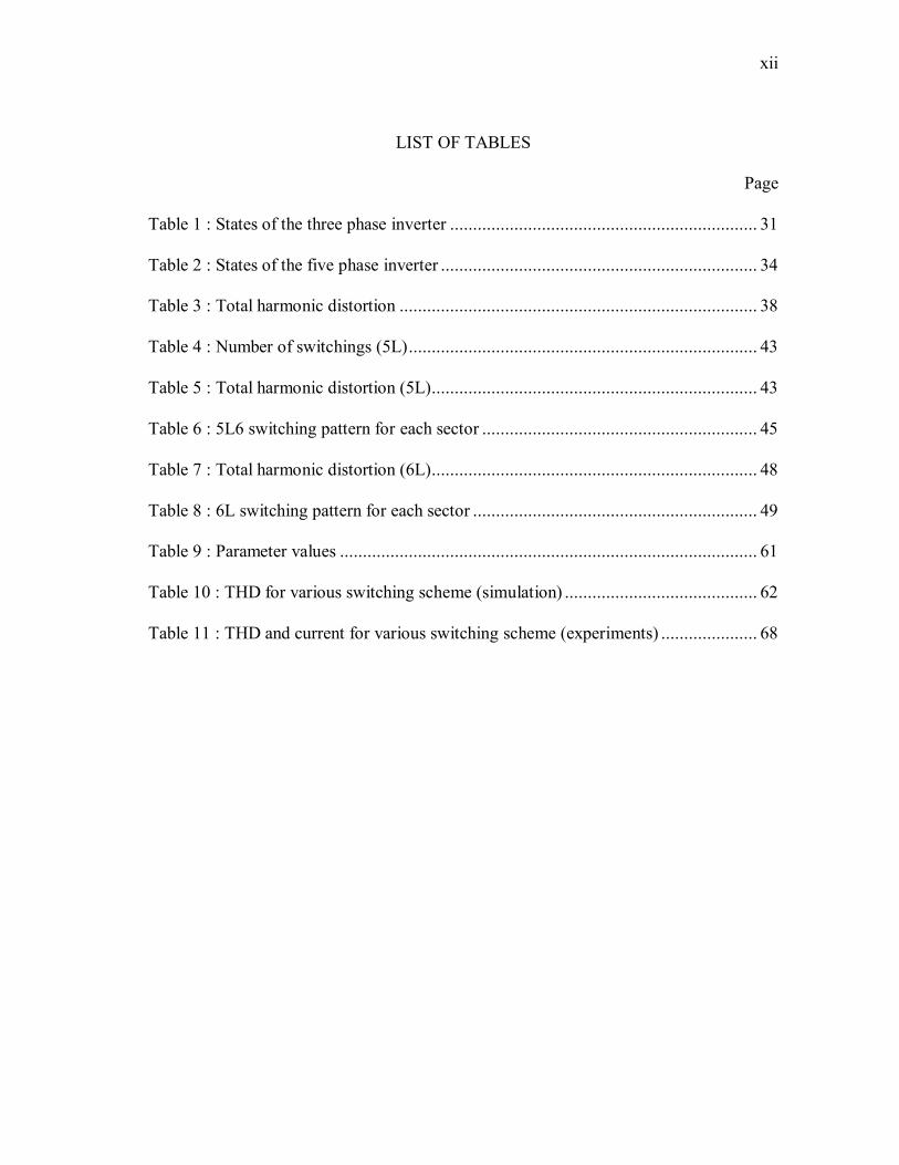
motor. Fig. 1 shows the most common causes of bearing failure and the percentage of its
occurrence. It shows that 9% of bearing failure is due to bearing currents.
In this thesis, the bearing currents in five-phase induction motors are studied. The
causes and solutions are reviewed. Then, a new solution is proposed and verified
experimentally.
____________ This thesis follows the style of IEEE Transactions on Industry Applications.

2
Fig. 1 : Reasons of bearing damage [1]
2. Shaft voltage generation
The theory behind shaft voltages and bearing currents is well understood today
[2] - [8]. In this section, the theory is reviewed and the system is modeled. This model
will be used later to simulate the system under different conditions.
In electrical machines, current flows in the windings to generate the magnetic
flux and rotate the shaft. Ideally, no current flows in the shaft or other mechanical
components. If an electrical current flow in the mechanical system for any reason, it may
cause problems. For instance, electrical currents can reduce bearing life time and
damage the bearing.
The problem of shaft voltages and bearing currents was discovered back in
1920’s [9], but solved by improving motor symmetry and manufacturing tolerances.
Recently, the problem was reported again when pulse width modulated (PWM) drives
3
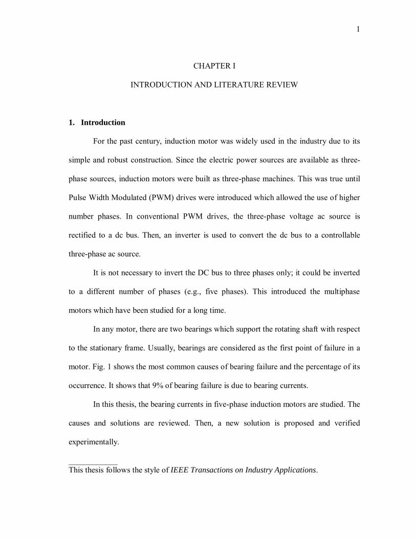
were installed. Some common symptoms that indicate the existence of bearing current
include: blackening the oil, scoring the shaft, noise, and pitting and fluting the bearing as
shown in Fig. 2:
Fig. 2 : Fluting the bearing [10]
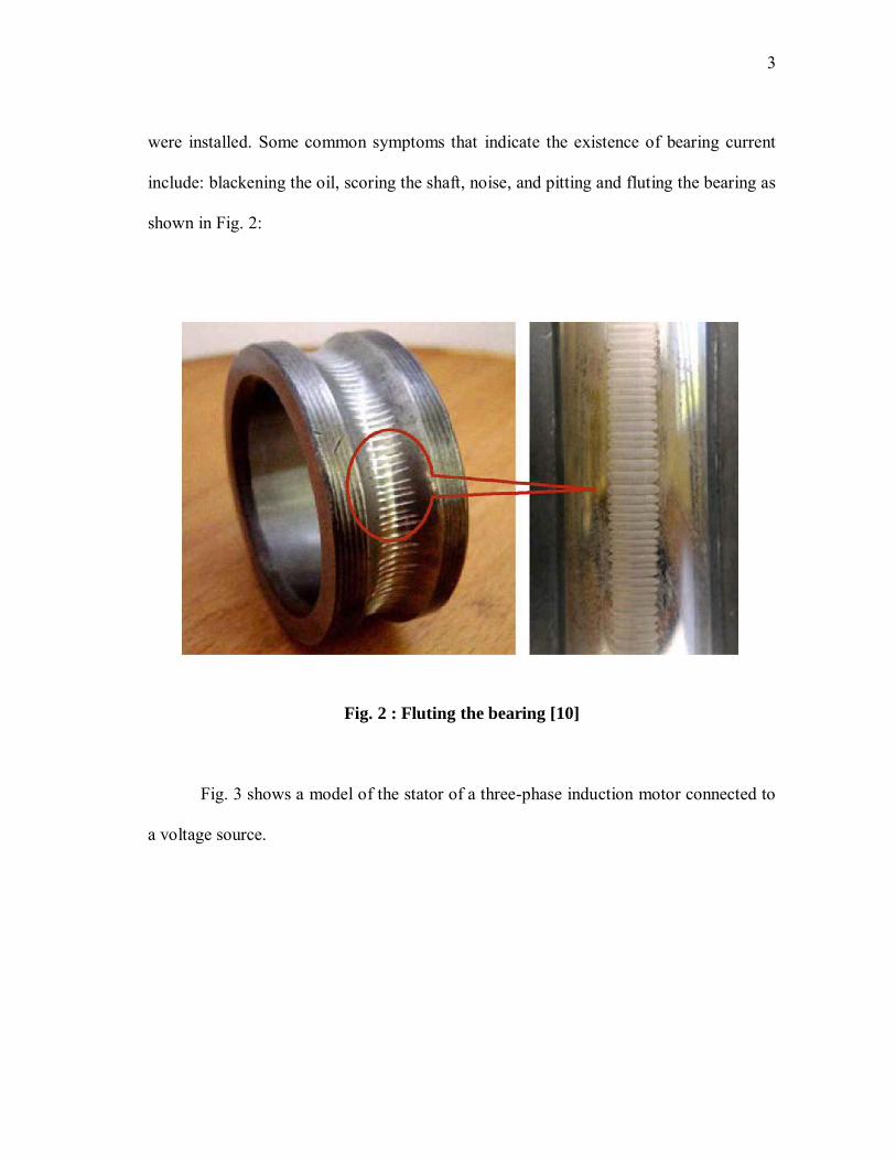
Fig. 3 shows a model of the stator of a three-phase induction motor connected to
a voltage source.
4
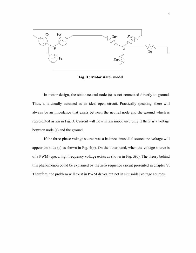
Fig. 3 : Motor stator model
In motor design, the stator neutral node (s) is not connected directly to ground.
Thus, it is usually assumed as an ideal open circuit. Practically speaking, there will
always be an impedance that exists between the neutral node and the ground which is
represented as Zn in Fig. 3. Current will flow in Zn impedance only if there is a voltage
between node (s) and the ground.
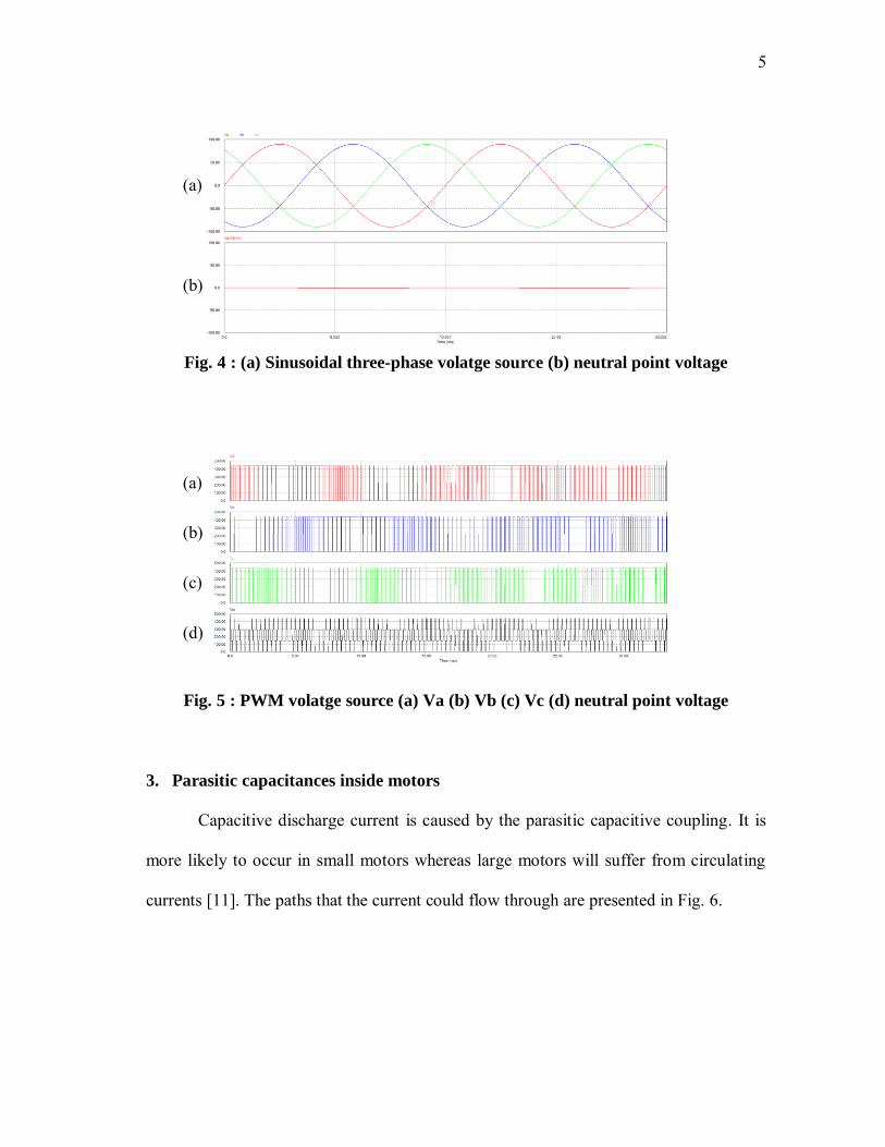
If the three-phase voltage source was a balance sinusoidal source, no voltage will
appear on node (s) as shown in Fig. 4(b). On the other hand, when the voltage source is
of a PWM type, a high frequency voltage exists as shown in Fig. 5(d). The theory behind
this phenomenon could be explained by the zero sequence circuit presented in chapter V.
Therefore, the problem will exist in PWM drives but not in sinusoidal voltage sources.
VaVb
Vc
Zw Zw
Zw
Zng s
5
Fig. 4 : (a) Sinusoidal three-phase volatge source (b) neutral point voltage
Fig. 5 : PWM volatge source (a) Va (b) Vb (c) Vc (d) neutral point voltage
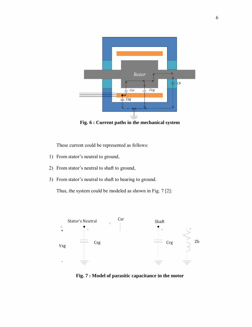
3. Parasitic capacitances inside motors
Capacitive discharge current is caused by the parasitic capacitive coupling. It is
more likely to occur in small motors whereas large motors will suffer from circulating
currents [11]. The paths that the current could flow through are presented in Fig. 6.
(a)
(b)
(a)
(b)
(c)
(d)
6
Fig. 6 : Current paths in the mechanical system
These current could be represented as follows:
1) From stator’s neutral to ground,
2) From stator’s neutral to shaft to ground,
3) From stator’s neutral to shaft to bearing to ground.
Thus, the system could be modeled as shown in Fig. 7 [2]:
Fig. 7 : Model of parasitic capacitance in the motor
7
Where,
Csg is the capacitance between stator’s neutral and ground,
Csr is the capacitance between stator’s neutral and shaft,
Crg is the capacitance between shaft and ground,
Zb is the impedance of the bearing.
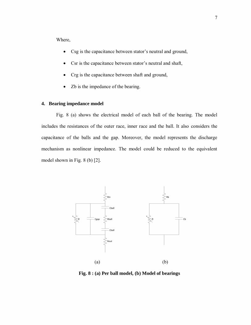
4. Bearing impedance model
Fig. 8 (a) shows the electrical model of each ball of the bearing. The model
includes the resistances of the outer race, inner race and the ball. It also considers the
capacitance of the balls and the gap. Moreover, the model represents the discharge
mechanism as nonlinear impedance. The model could be reduced to the equivalent
model shown in Fig. 8 (b) [2].
(a) (b)
Fig. 8 : (a) Per ball model, (b) Model of bearings
Rout
Cball
Rball
Cball
Rin
CgapZl
Rb
CbZl
8
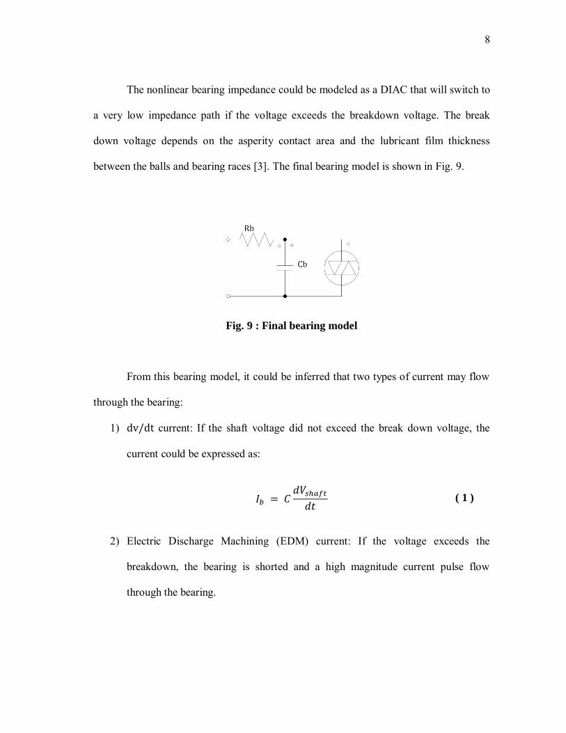
The nonlinear bearing impedance could be modeled as a DIAC that will switch to
a very low impedance path if the voltage exceeds the breakdown voltage. The break
down voltage depends on the asperity contact area and the lubricant film thickness
between the balls and bearing races [3]. The final bearing model is shown in Fig. 9.
Fig. 9 : Final bearing model
From this bearing model, it could be inferred that two types of current may flow
through the bearing:
1) current: If the shaft voltage did not exceed the break down voltage, the
current could be expressed as:
( 1 )
2) Electric Discharge Machining (EDM) current: If the voltage exceeds the
breakdown, the bearing is shorted and a high magnitude current pulse flow
through the bearing.

9
5. Solutions to the problem
Presently, many solutions are suggested to this problem. These include:
A. Bearing insulation
Insulating the bearings will increase the resistance of the bearing and reduces the
current flow. It may be implemented in two ways: insulating both bearing’s pedestals or
by using hybrid bearing (Ceramic balls). It should be noted, however, that this will only
transfer the problem to the coupling and load. Therefore, the coupling should be
insulated too.
B. Shaft grounding
Grounding the shaft will provide an alternative path for the current to flow in. It
is applied in three methods:
1) Grounding brush,
2) Grommet,
3) Ring.
C. Conductive grease
Conductive grease will short the current and no high discharge current will flow.
The main problem with this method is that conductive particles in these lubricants
increase mechanical wear to the bearing.
D. dv/dt filter
Common mode reactor could be used in series with the motor in two ways:
1. Active cancellation,
2. Low-pass filtering.

10
E. Faraday shield
A grounded conductive material installed between rotor and stator creates a
Faraday shield. It reduces capacitive coupled currents across the air gap and minimizes
shaft voltage [4].
F. Shielded three-phase cable
A shielded cable can improve the high frequency grounding by providing a low
impedance path between the drive and the motor.
G. New inverter topology
Using a five-phase control method to reduce neutral’s stator voltage and thus
EDM bearing currents. One crucial and successful way, is to modify the switching
scheme. This will be the topic presented in the following chapters.
11
CHAPTER II
QD0 TRANSFORMATION
1. Introduction
The qd0 transformation is commonly used to simplify the analysis of machine
models. Basically, it transforms the three phases to two-phase system. In multiphase
machines, the transformation will lead to multiple two-phase systems.
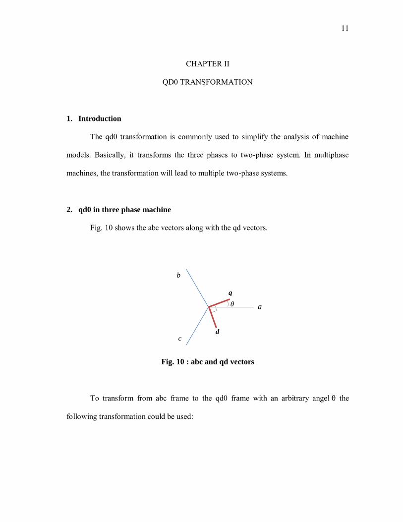
2. qd0 in three phase machine
Fig. 10 shows the abc vectors along with the qd vectors.
Fig. 10 : abc and qd vectors
To transform from abc frame to the qd0 frame with an arbitrary angel the
following transformation could be used:
𝜃 a
b
c d
q
12
[
]
[ ( ) (
) (
)
( ) (
) (
)
]
[
] ( 2 )
Or simply,
( ) ( 3 )
Where ( ) is the transformation matrix and could represents the voltage,
current or flux linkage of either the stator or the rotor. Taking the inverse,
[
]
[
( ) ( )
(
) (
)
(
) (
) ]
[
] ( 4 )
( ) ( 5 )
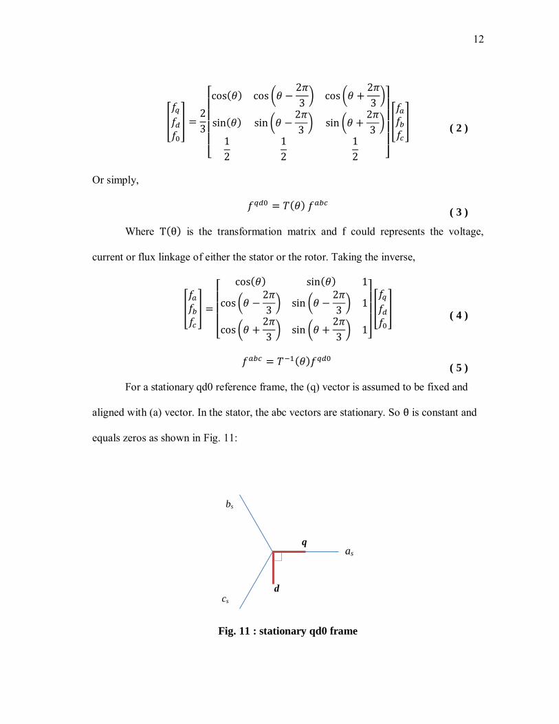
For a stationary qd0 reference frame, the (q) vector is assumed to be fixed and
aligned with (a) vector. In the stator, the abc vectors are stationary. So is constant and
equals zeros as shown in Fig. 11:
Fig. 11 : stationary qd0 frame
as
bs
cs d
q
13
Substitute in ( 2 ) results in the stationary transformation given by,
( )
[
√
√
]
( 6 )
Then the transformation matrices for the voltage, current and flux linkage of the
stator variables could be written as:
( )
( 7 )
( )
( 8 )
( )
( 9 )
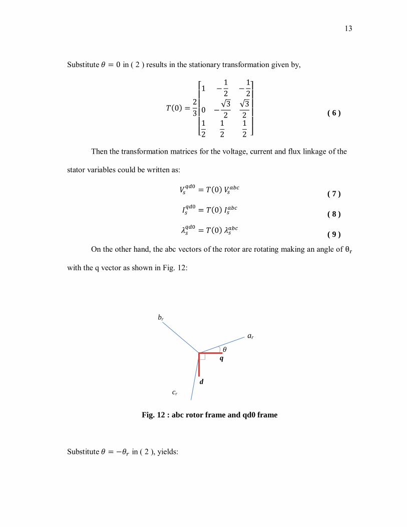
On the other hand, the abc vectors of the rotor are rotating making an angle of
with the q vector as shown in Fig. 12:
Fig. 12 : abc rotor frame and qd0 frame
Substitute in ( 2 ), yields:
ar
br
cr
d
q 𝜃
14
( )
[ ( ) (
) (
)
( ) (
) (
)
]
( 10 )
Then the transfer functions for the voltage, current and flux linkage in the stator
could be written as:
( )
( 11 )
( ) ( 12 )
( ) ( 13 )
3. Expanding qd0 transformation to five-phase system
In an N phase system, the transformation will lead to N sequences as explained in
[12]. The first sequence is spaced by
and the second is spaced by
. The final
sequence will results in spacing of which means that all phases are in the same
direction; this is called the zero sequence.
Thus, a five-phase system will result in five sequences. These five sequences will
be spaced by
as shown in Fig. 13.
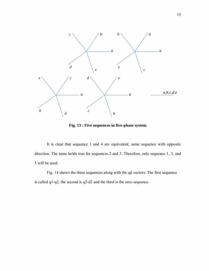
15
Fig. 13 : Five sequences in five-phase system
It is clear that sequence 1 and 4 are equivalent; same sequence with opposite
direction. The same holds true for sequences 2 and 3. Therefore, only sequence 1, 3, and
5 will be used.
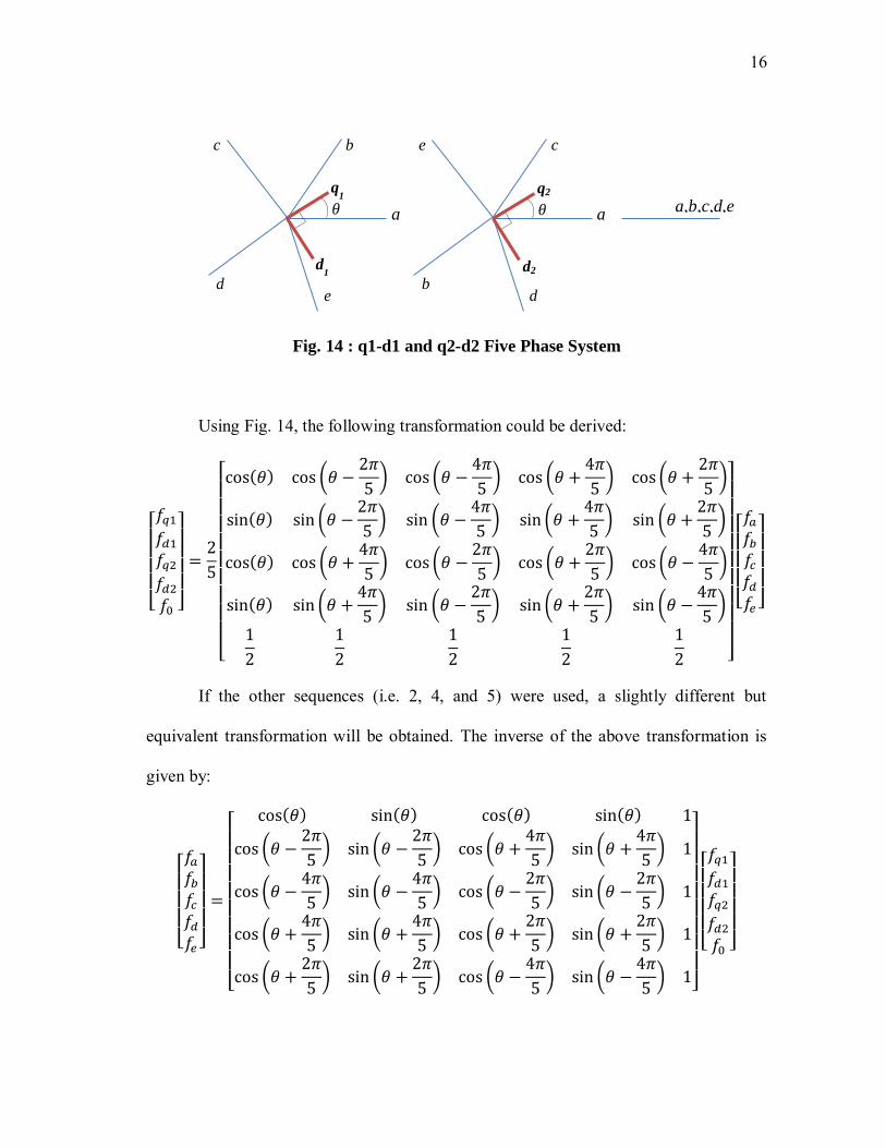
Fig. 14 shows the three sequences along with the qd vectors. The first sequence
is called q1-q2, the second is q2-d2 and the third is the zero sequence.
a
c
d
b
e
a
b
e
d
c
a
e
b
c
d
a
d
c
e
b
a,b,c,d,e
16
Fig. 14 : q1-d1 and q2-d2 Five Phase System
Using Fig. 14, the following transformation could be derived:
[
]
[ ( ) (
) (
) (
) (
)
( ) (
) (
) (
) (
)
( ) (
) (
) (
) (
)
( ) (
) (
) (
) (
)
]
[ ]
If the other sequences (i.e. 2, 4, and 5) were used, a slightly different but
equivalent transformation will be obtained. The inverse of the above transformation is
given by:
[ ]
[
( ) ( ) ( ) ( )
(
) (
) (
) (
)
(
) (
) (
) (
)
(
) (
) (
) (
)
(
) (
) (
) (
) ]
[
]
a
c
d
b
e
q1
d1
a
e
b
c
d
d2
q2 a,b,c,d,e

17
Stationary qd0 transformation could be obtained by substituting in the
above expressions:
[
]
[ (
) (
) (
) (
)
(
) (
) (
) (
)
(
) (
) (
) (
)
(
) (
) (
) (
)
]
[ ]
( 14 )
4. Properties of the qd0 transformation
In this section, two important properties of the qd0 transformation will be
presented. These properties will be used later to derive the model of the induction motor.
These two properties are:
( )
( )
[
]
( 15 )
( )
[ (
) (
) (
) (
)
(
) (
) (
) (
)
(
) (
) (
) (
)
(
) (
) (
) (
)
(
) (
) (
) (
)
]
( )
[ ]
( 16 )
18
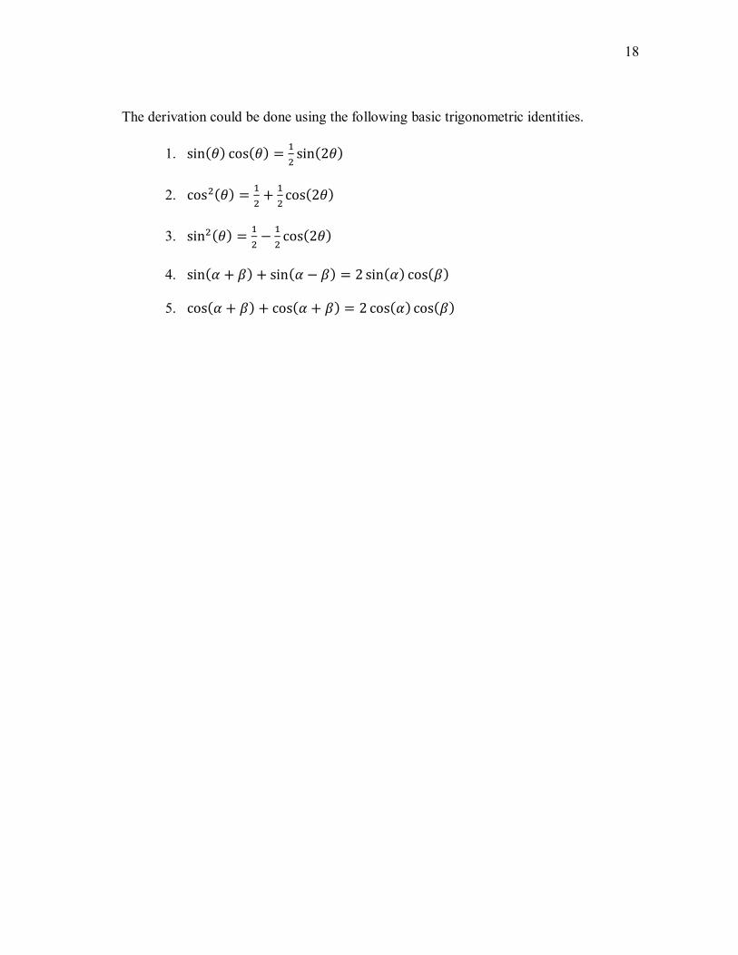
The derivation could be done using the following basic trigonometric identities.
1. ( ) ( )
( )
2. ( )
( )
3. ( )
( )
4. ( ) ( ) ( ) ( )
5. ( ) ( ) ( ) ( )
19
CHAPTER III
FIVE PHASE INDUCTION MOTOR MODEL
In this chapter, the model of the five-phase induction motor is derived. The
derivation is similar to the three phase case but involve more complex math. The model
of five-phase induction motor was first introduced in [13].
1. Voltage, current and flux linkage
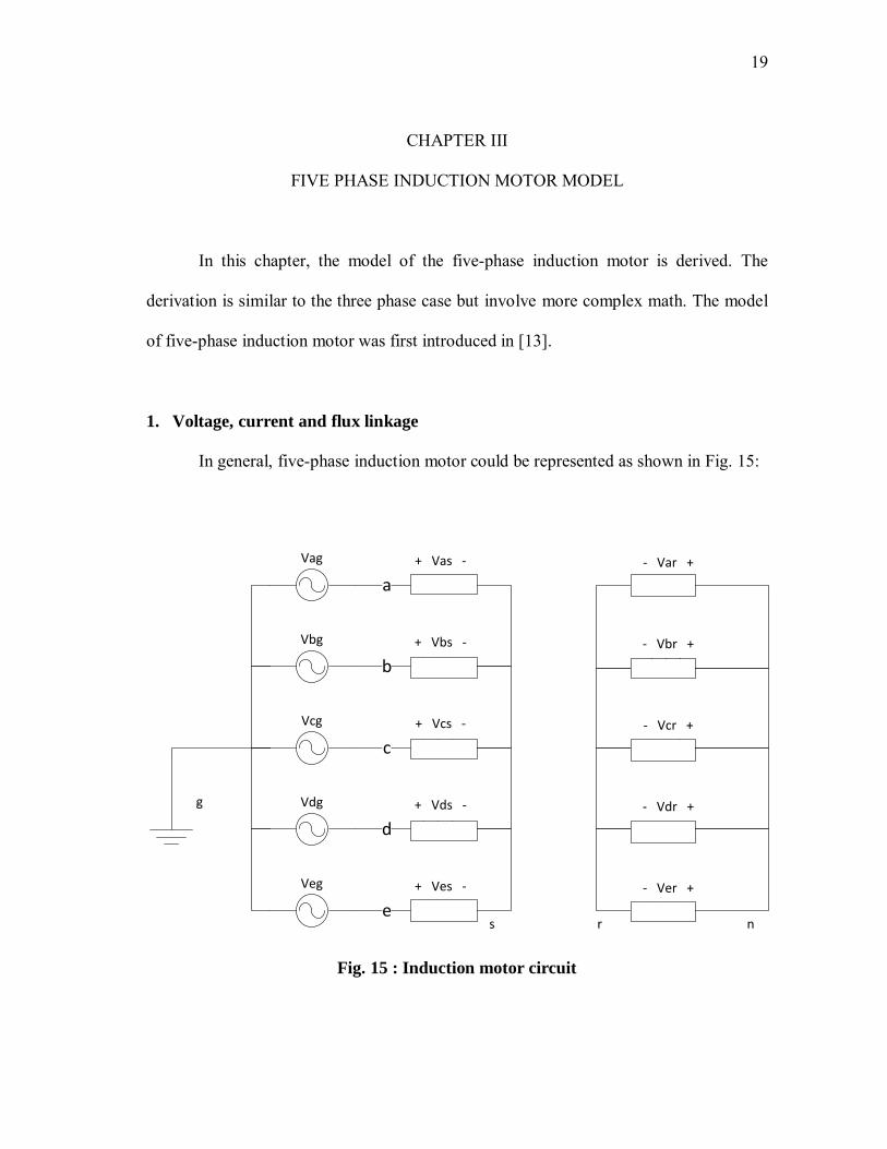
In general, five-phase induction motor could be represented as shown in Fig. 15:
Fig. 15 : Induction motor circuit
Vag
Vbg
Vcg
Vdg
Veg
g
e
d
c
b
a
s
+ Vas -
+ Vbs -
+ Vcs -
+ Vds -
+ Ves -
nr
- Var +
- Vbr +
- Vcr +
- Vdr +
- Ver +
20
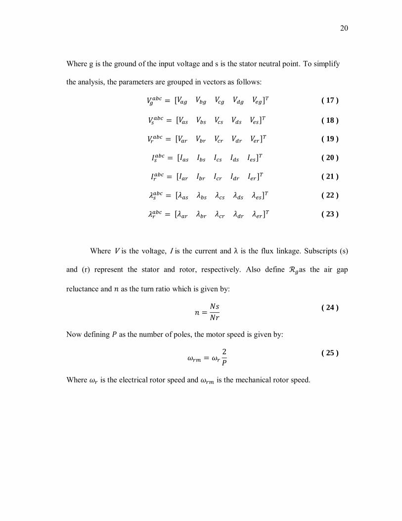
Where g is the ground of the input voltage and s is the stator neutral point. To simplify
the analysis, the parameters are grouped in vectors as follows:
[ ] ( 17 )
[ ] ( 18 )
[ ] ( 19 )
[ ] ( 20 )
[ ] ( 21 )
[ ]
( 22 )
[ ]
( 23 )
Where V is the voltage, I is the current and is the flux linkage. Subscripts (s)
and (r) represent the stator and rotor, respectively. Also define as the air gap
reluctance and as the turn ratio which is given by:
( 24 )
Now defining as the number of poles, the motor speed is given by:
( 25 )
Where is the electrical rotor speed and is the mechanical rotor speed.
21
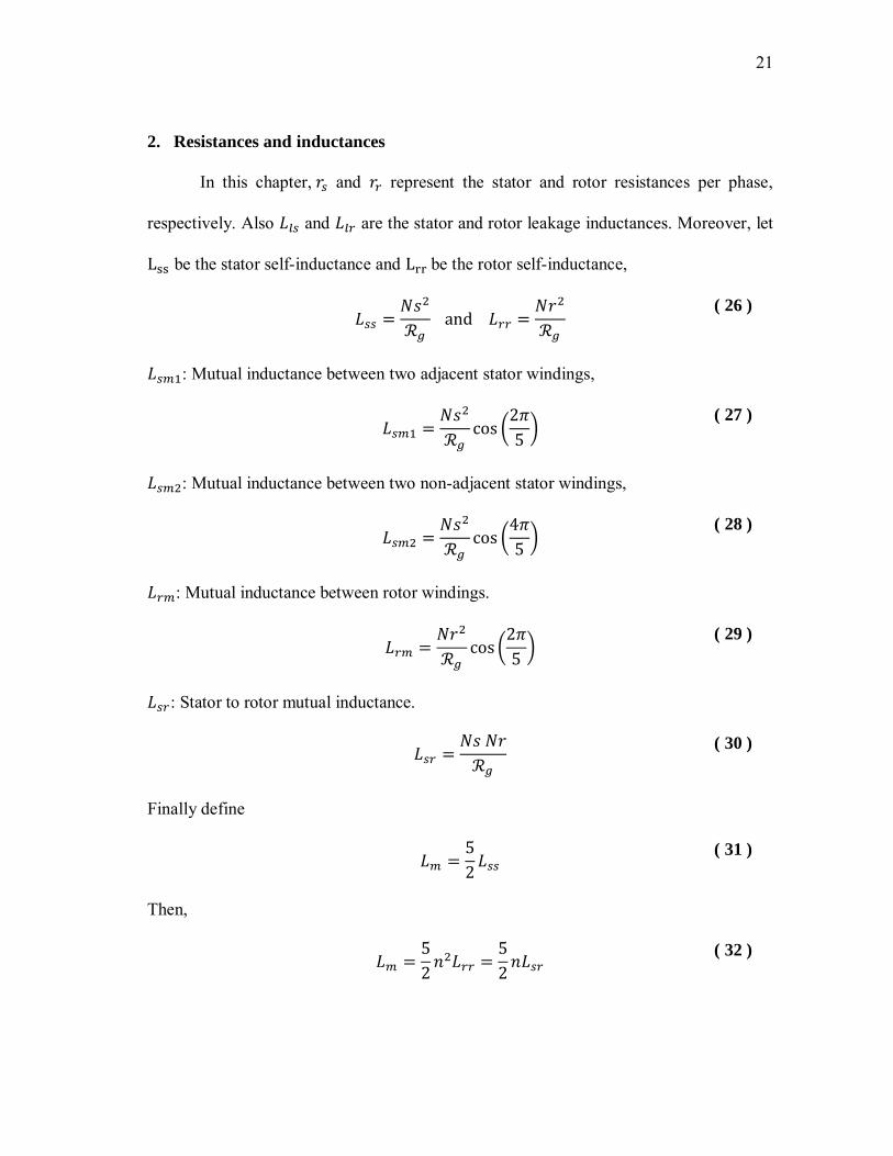
2. Resistances and inductances
In this chapter, and represent the stator and rotor resistances per phase,
respectively. Also and are the stator and rotor leakage inductances. Moreover, let
be the stator self-inductance and be the rotor self-inductance,
( 26 )
: Mutual inductance between two adjacent stator windings,
(
)
( 27 )
: Mutual inductance between two non-adjacent stator windings,
(
)
( 28 )
: Mutual inductance between rotor windings.
(
)
( 29 )
: Stator to rotor mutual inductance.
( 30 )
Finally define
( 31 )
Then,
( 32 )
22
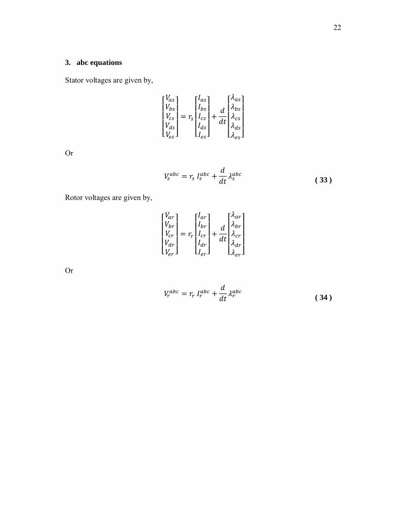
3. abc equations
Stator voltages are given by,
[
]
[
]
[
]
Or
( 33 )
Rotor voltages are given by,
[
]
[
]
[
]
Or
( 34 )
23
Stator flux linkage:
[
]
[
]
[
]
[ ( ) (
) (
) (
) (
)
(
) ( ) (
) (
) (
)
(
) (
) ( ) (
) (
)
(
) (
) (
) ( ) (
)
(
) (
) (
) (
) ( ) ]
[
]
Or,
( 35 )
Rotor Flux linkage:
[
]
[ ( ) (
) (
) (
) (
)
(
) ( ) (
) (
) (
)
(
) (
) ( ) (
) (
)
(
) (
) (
) ( ) (
)
(
) (
) (
) (
) ( ) ]
[
]
[
]
[
]
( 36 )
Noting that,
[
]
24
4. qd0 equations
A. Stator voltage
The stator voltage vector in the qd0 frame is given by:
( ) ( )
( )
( ) ( )
( )
( ( )
)
( ) ( )
( )
( )
( ) ( )
Since , then the middle term will be zero:
( 37 )
B. Rotor voltage
Similarly,
( ) ( )
( )
( ) ( )
( )
( ( )
)
( ) ( )
( )
( )
( ) ( )
Again using the property of the transformation with :
[
]
( 38 )
25
C. Stator flux linkage
Using ( 9 ) and ( 35 ):
( ) ( )
( )
( ) ( )
( )
( )
By definition, it could be rewritten as:
( 39 )
Where,
( ) ( )
( )
[
( )
[ ]
[ (
) (
) (
) (
)
(
) (
) (
) (
)
(
) (
) (
) (
)
(
) (
) (
) (
)
(
) (
) (
) (
) ]
]
( )
Using the properties of qd0 transformation:
[ ]
[ ]
[
]
Moreover, using trigonometric identities, it could be shown that
( ) ( )
[
]
26
D. Rotor flux linkage
Using ( 13 ) and ( 36 ):
( ) ( )
( )
Now using the inverse of ( 8 ) and ( 12 ):
( ) ( )
( )
( )
( 40 )
Where,
( ) ( )
( )
[
[ ]
[ (
) (
) (
) (
)
(
) (
) (
) (
)
(
) (
) (
) (
)
(
) (
) (
) (
)
(
) (
) (
) (
) ]
]
( )
Again,
[ ]
[ ]
[
]
And,
( ) ( )
[
]
27
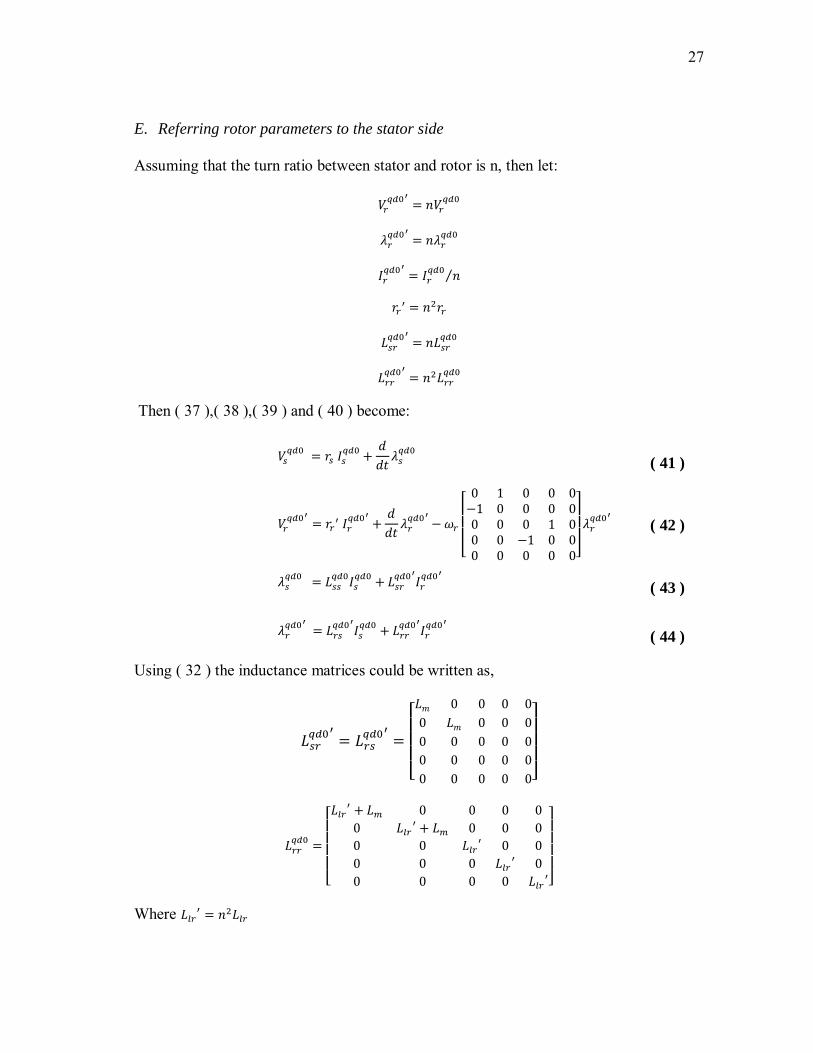
E. Referring rotor parameters to the stator side
Assuming that the turn ratio between stator and rotor is n, then let:
⁄
Then ( 37 ),( 38 ),( 39 ) and ( 40 ) become:
( 41 )
[
]
( 42 )
( 43 )
( 44 )
Using ( 32 ) the inductance matrices could be written as,
[
]
[
]
Where

28
5. qd0 torque and speed
The input power could be expressed as:
Substitute ( 41 ) and ( 42 ) for the voltages:
(
)
The power converted to mechanical work is represented by the last two terms only:
(
)
(
)
(
( )
( )
)
(
)
( 45 )
Finally, the speed could be determined as follows:
( )
( )
( 46 )
29
CHAPTER IV
INVERTER MODEL
1. Introduction
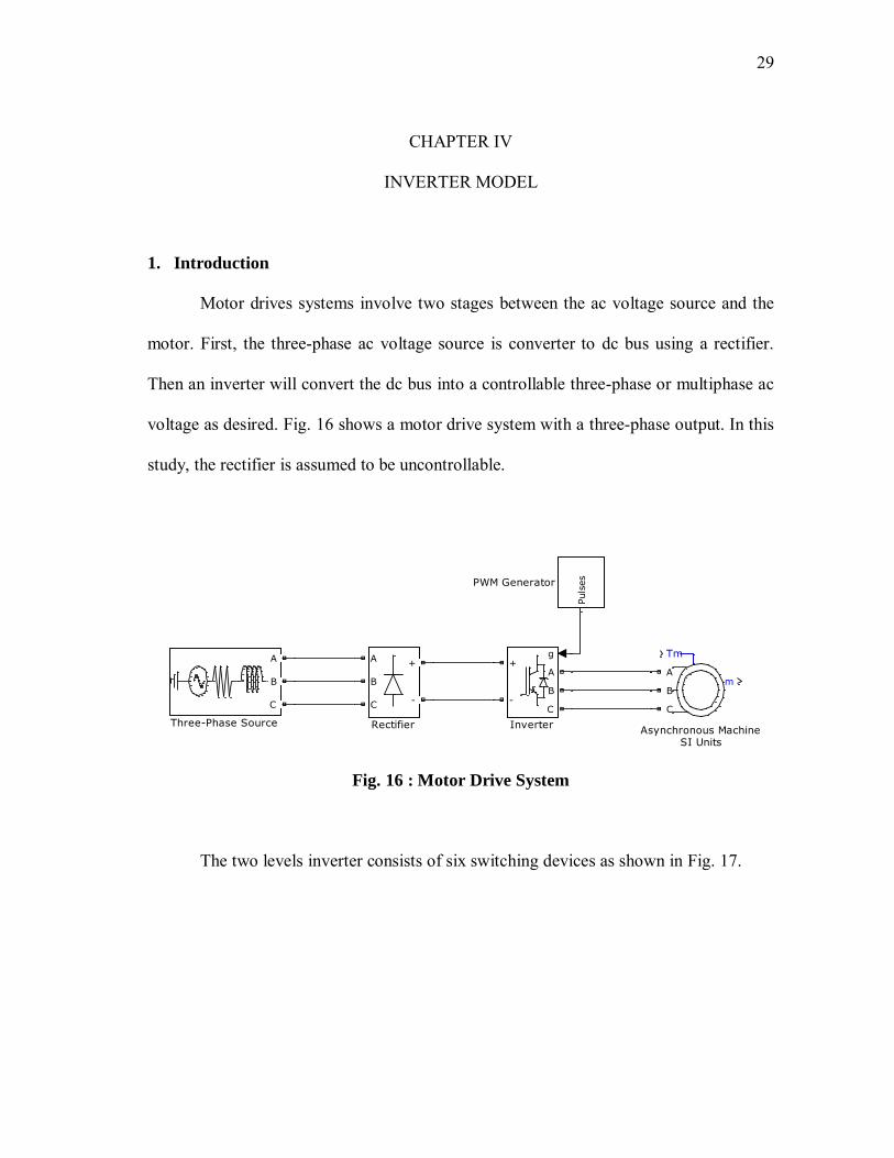
Motor drives systems involve two stages between the ac voltage source and the
motor. First, the three-phase ac voltage source is converter to dc bus using a rectifier.
Then an inverter will convert the dc bus into a controllable three-phase or multiphase ac
voltage as desired. Fig. 16 shows a motor drive system with a three-phase output. In this
study, the rectifier is assumed to be uncontrollable.
Fig. 16 : Motor Drive System
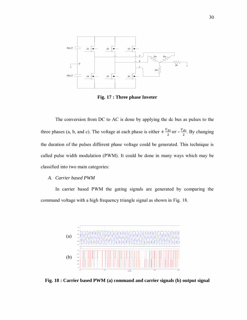
The two levels inverter consists of six switching devices as shown in Fig. 17.
A
B
C
Three-Phase Source
A
B
C
+
-
Rectifier
Puls
es
PWM Generator
g
A
B
C
+
-
Inverter
mA
B
C
Tm
Asynchronous MachineSI Units
30
Fig. 17 : Three phase Inveter
The conversion from DC to AC is done by applying the dc bus as pulses to the
three phases (a, b, and c). The voltage at each phase is either
–
. By changing
the duration of the pulses different phase voltage could be generated. This technique is
called pulse width modulation (PWM). It could be done in many ways which may be
classified into two main categories:
A. Carrier based PWM
In carrier based PWM the gating signals are generated by comparing the
command voltage with a high frequency triangle signal as shown in Fig. 18.
Fig. 18 : Carrier based PWM (a) command and carrier signals (b) output signal
Zw Zw
Zw
Zn
a
b
c
Vdc/2
Vdc/2
O
S1 S2 S3
S4 S5 S6
(a)
(b)

31
B. Space Vector PWM
In each leg of Fig. 17, if the upper switch is ON then it is marked as 1 and if the
lower one is ON it is 0. Space vector pulse width modulation (SVPWM) is a technique
where the all of inverter switching possibilities are listed as sets. Each set contains a
combination of 1’s and 0’s that is equal to the number of phases. Thus, the total number
of set is given by 2# of phases. Table 1 shows all the possible combination for three-phase
system.
Table 1 : States of the three phase inverter
Switches Inverter Phase Voltages (x Vdc) Inverter Line Voltages (x Vdc)
S1 S2 S3 Vao Vbo Vco Vo Vab Vbc Vca
0 0 0 0 - 1/2 - 1/2 - 1/2 - 1/2 0 0 0
1 0 0 1 - 1/2 - 1/2 1/2 - 1/6 0 -1 1
2 0 1 0 - 1/2 1/2 - 1/2 - 1/6 -1 1 0
3 0 1 1 - 1/2 1/2 1/2 1/6 -1 0 1
4 1 0 0 1/2 - 1/2 -1/2 - 1/6 1 0 -1
5 1 0 1 1/2 - 1/2 1/2 1/6 1 -1 0
6 1 1 0 1/2 1/2 -1/2 1/6 0 1 -1
7 1 1 1 1/2 1/2 1/2 1/2 0 0 0
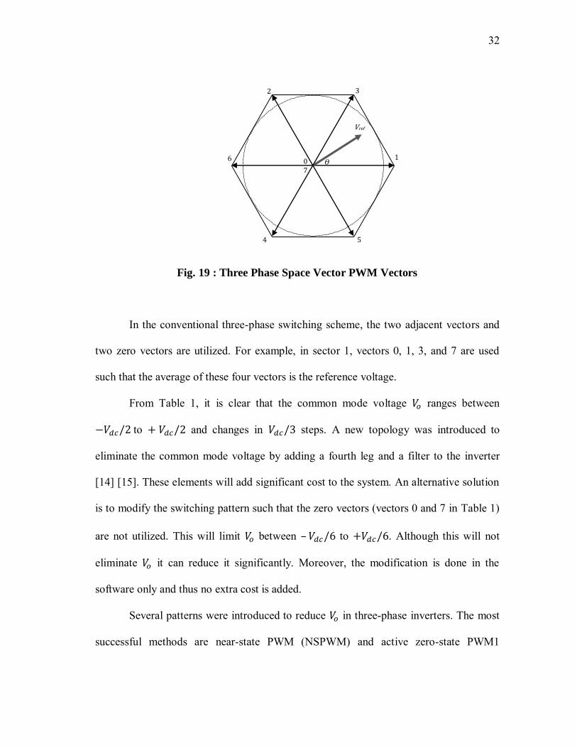
Each set could be represented as a vector as shown in Fig. 19. For each of the six
sectors, specific vectors are chosen. Afterwards, depending on the required reference
voltage, each vector is given a duty ratio such that the average weight of the chosen
vectors is equal to the reference voltage.
32
Fig. 19 : Three Phase Space Vector PWM Vectors
In the conventional three-phase switching scheme, the two adjacent vectors and
two zero vectors are utilized. For example, in sector 1, vectors 0, 1, 3, and 7 are used
such that the average of these four vectors is the reference voltage.
From Table 1, it is clear that the common mode voltage ranges between
to and changes in steps. A new topology was introduced to
eliminate the common mode voltage by adding a fourth leg and a filter to the inverter
[14] [15]. These elements will add significant cost to the system. An alternative solution
is to modify the switching pattern such that the zero vectors (vectors 0 and 7 in Table 1)
are not utilized. This will limit between – to . Although this will not
eliminate it can reduce it significantly. Moreover, the modification is done in the
software only and thus no extra cost is added.
Several patterns were introduced to reduce in three-phase inverters. The most
successful methods are near-state PWM (NSPWM) and active zero-state PWM1
1
2 3
4 5
6 0 7
Vref
𝛳
33
(AZSPWM1) methods which are discussed in [16]. NSPWM has limited dc bus
utilization. In some cases, AZSPWM1 may require that two inverter legs switch
simultaneously which is not practical.
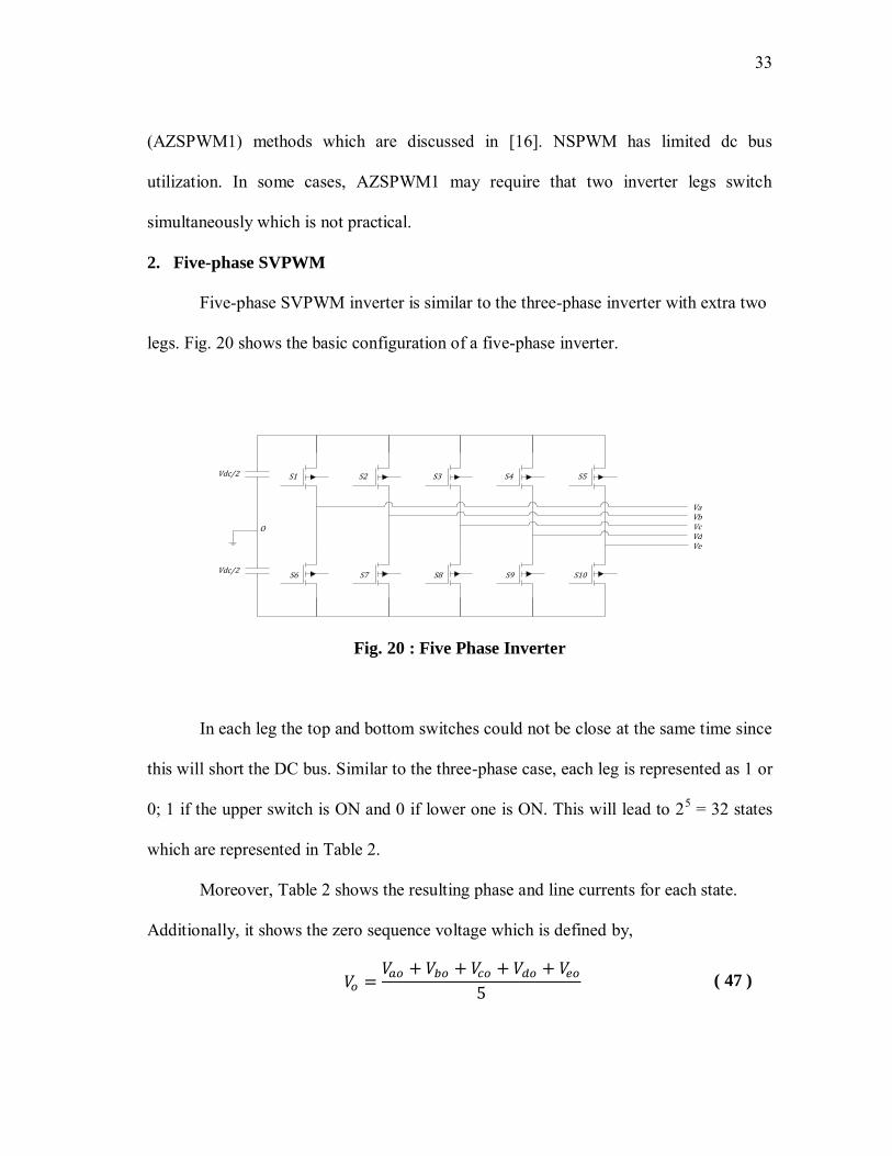
2. Five-phase SVPWM
Five-phase SVPWM inverter is similar to the three-phase inverter with extra two
legs. Fig. 20 shows the basic configuration of a five-phase inverter.
Fig. 20 : Five Phase Inverter
In each leg the top and bottom switches could not be close at the same time since
this will short the DC bus. Similar to the three-phase case, each leg is represented as 1 or
0; 1 if the upper switch is ON and 0 if lower one is ON. This will lead to 25 = 32 states
which are represented in Table 2.
Moreover, Table 2 shows the resulting phase and line currents for each state.
Additionally, it shows the zero sequence voltage which is defined by,
( 47 )
VaVbVcVdVe
Vdc/2
Vdc/2
O
S1 S2 S3 S4 S5
S6 S7 S8 S9 S10

34
Table 2 : States of the five phase inverter
Switches Inverter Phase Voltages (x VDC) Inverter Line Voltages (x VDC)
S1 S2 S3 S4 S5 Vao Vbo Vco Vdo Veo Vo Vab Vbc Vcd Vde Vea
0 0 0 0 0 0 - 1/2 - 1/2 - 1/2 - 1/2 - 1/2 -0.5 0 0 0 0 0
1 0 0 0 0 1 - 1/2 - 1/2 - 1/2 - 1/2 1/2 -0.3 0 0 0 -1 1
2 0 0 0 1 0 - 1/2 - 1/2 - 1/2 1/2 - 1/2 -0.3 0 0 -1 1 0
3 0 0 0 1 1 - 1/2 - 1/2 - 1/2 1/2 1/2 -0.1 0 0 -1 0 1
4 0 0 1 0 0 - 1/2 - 1/2 1/2 - 1/2 - 1/2 -0.3 0 -1 1 0 0
5 0 0 1 0 1 - 1/2 - 1/2 1/2 - 1/2 1/2 -0.1 0 -1 1 -1 1
6 0 0 1 1 0 - 1/2 - 1/2 1/2 1/2 - 1/2 -0.1 0 -1 0 1 0
7 0 0 1 1 1 - 1/2 - 1/2 1/2 1/2 1/2 0.1 0 -1 0 0 1
8 0 1 0 0 0 - 1/2 1/2 - 1/2 - 1/2 - 1/2 -0.3 -1 1 0 0 0
9 0 1 0 0 1 - 1/2 1/2 - 1/2 - 1/2 1/2 -0.1 -1 1 0 -1 1
10 0 1 0 1 0 - 1/2 1/2 - 1/2 1/2 - 1/2 -0.1 -1 1 -1 1 0
11 0 1 0 1 1 - 1/2 1/2 - 1/2 1/2 1/2 0.1 -1 1 -1 0 1
12 0 1 1 0 0 - 1/2 1/2 1/2 - 1/2 - 1/2 -0.1 -1 0 1 0 0
13 0 1 1 0 1 - 1/2 1/2 1/2 - 1/2 1/2 0.1 -1 0 1 -1 1
14 0 1 1 1 0 - 1/2 1/2 1/2 1/2 - 1/2 0.1 -1 0 0 1 0
15 0 1 1 1 1 - 1/2 1/2 1/2 1/2 1/2 0.3 -1 0 0 0 1
16 1 0 0 0 0 1/2 - 1/2 - 1/2 - 1/2 - 1/2 -0.3 1 0 0 0 -1
17 1 0 0 0 1 1/2 - 1/2 - 1/2 - 1/2 1/2 -0.1 1 0 0 -1 0
18 1 0 0 1 0 1/2 - 1/2 - 1/2 1/2 - 1/2 -0.1 1 0 -1 1 -1
19 1 0 0 1 1 1/2 - 1/2 - 1/2 1/2 1/2 0.1 1 0 -1 0 0
20 1 0 1 0 0 1/2 - 1/2 1/2 - 1/2 - 1/2 -0.1 1 -1 1 0 -1
21 1 0 1 0 1 1/2 - 1/2 1/2 - 1/2 1/2 0.1 1 -1 1 -1 0
22 1 0 1 1 0 1/2 - 1/2 1/2 1/2 - 1/2 0.1 1 -1 0 1 -1
23 1 0 1 1 1 1/2 - 1/2 1/2 1/2 1/2 0.3 1 -1 0 0 0
24 1 1 0 0 0 1/2 1/2 - 1/2 - 1/2 - 1/2 -0.1 0 1 0 0 -1
25 1 1 0 0 1 1/2 1/2 - 1/2 - 1/2 1/2 0.1 0 1 0 -1 0
26 1 1 0 1 0 1/2 1/2 - 1/2 1/2 - 1/2 0.1 0 1 -1 1 -1
27 1 1 0 1 1 1/2 1/2 - 1/2 1/2 1/2 0.3 0 1 -1 0 0
28 1 1 1 0 0 1/2 1/2 1/2 - 1/2 - 1/2 0.1 0 0 1 0 -1
29 1 1 1 0 1 1/2 1/2 1/2 - 1/2 1/2 0.3 0 0 1 -1 0
30 1 1 1 1 0 1/2 1/2 1/2 1/2 - 1/2 0.3 0 0 0 1 -1
31 1 1 1 1 1 1/2 1/2 1/2 1/2 1/2 0.5 0 0 0 0 0

35
Using the qd0 transformation presented in Chapter II, these 32 states are
represented as vectors on the q1-d1 and q2-d2 frames as shown in Fig. 21.
Fig. 21 : The 32 states represented on q1-d1 and q2-d2.
These 32 states could be classified in four categories according to the vector length:
1. 10 Large vectors with length L,
2. 10 Medium vectors with length M,
3. 10 Small vectors with length S,
4. 2 Zero vectors with zero lengths.
Where L, M and S are given by:
36
(
)
(
)
( 48 )
For a reference voltage with a magnitude and angle , the current sector is
given by:
(
⁄ ) ( 49 )
Where represent the round toward positive infinity and:
( 50 )
Then, values for the current sector could be calculated as follows:
( ( )
) ( 51 )
( ( )
) ( 52 )
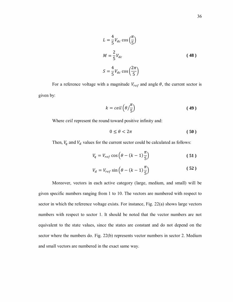
Moreover, vectors in each active category (large, medium, and small) will be
given specific numbers ranging from 1 to 10. The vectors are numbered with respect to
sector in which the reference voltage exists. For instance, Fig. 22(a) shows large vectors
numbers with respect to sector 1. It should be noted that the vector numbers are not
equivalent to the state values, since the states are constant and do not depend on the
sector where the numbers do. Fig. 22(b) represents vector numbers in sector 2. Medium
and small vectors are numbered in the exact same way.

37
Fig. 22 : Vector Numbers in (a) Sector 1 and (b) Sector 2.
Furthermore, for each of the 30 active vectors, two angels are defined.
is the angel between the vector and the q axis in q1-d1 frame. While represents the
angel between the vector and the q axis in q2-d2 frame. is given by :
( )
( 53 )
By comparing Fig. 21(a) and Fig. 21(b), it could be inferred that the direction of
large and small vector in q1-d1 frame is mapped to q2-d2 frame in the following
direction:
( )
( 54 )
Where k is the sector number and n is the vector number. With large vectors are
mapped as small and vice versa. The direction in which medium vectors are mapped is
the opposite of that given in ( 54 ):
( )
( 55 )
9
10
1
2
3 4
5
6
7
8
q
d
8
9
10
1
2 3
4
5
6
7
q d
38
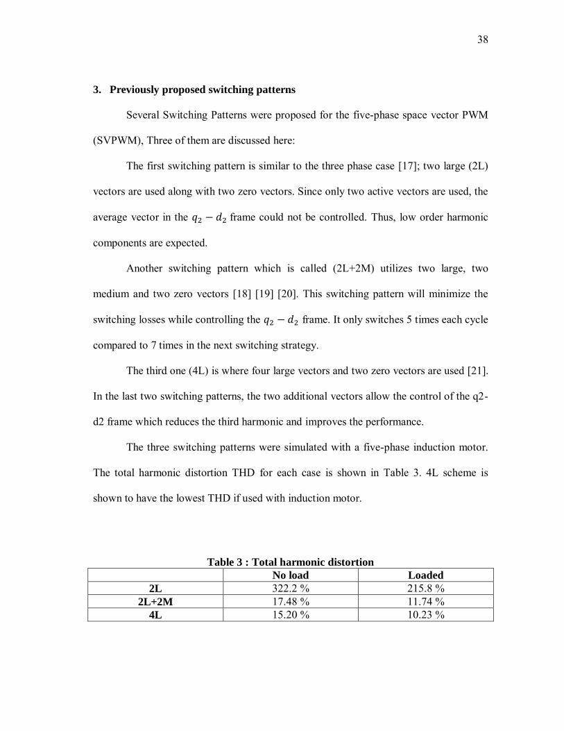
3. Previously proposed switching patterns
Several Switching Patterns were proposed for the five-phase space vector PWM
(SVPWM), Three of them are discussed here:
The first switching pattern is similar to the three phase case [17]; two large (2L)
vectors are used along with two zero vectors. Since only two active vectors are used, the
average vector in the frame could not be controlled. Thus, low order harmonic
components are expected.
Another switching pattern which is called (2L+2M) utilizes two large, two
medium and two zero vectors [18] [19] [20]. This switching pattern will minimize the
switching losses while controlling the frame. It only switches 5 times each cycle
compared to 7 times in the next switching strategy.
The third one (4L) is where four large vectors and two zero vectors are used [21].
In the last two switching patterns, the two additional vectors allow the control of the q2-
d2 frame which reduces the third harmonic and improves the performance.
The three switching patterns were simulated with a five-phase induction motor.
The total harmonic distortion THD for each case is shown in Table 3. 4L scheme is
shown to have the lowest THD if used with induction motor.
Table 3 : Total harmonic distortion
No load Loaded
2L 322.2 % 215.8 % 2L+2M 17.48 % 11.74 %
4L 15.20 % 10.23 %
39
4. Choosing switching vectors
In all previously proposed switching schemes, zero vectors were used. The new
switching scheme shall be chosen to reduce the zero sequence voltage . From Table 2,
it is obvious that the two zero vectors will produce the highest value of the zero
sequence voltage which is ⁄ . Additionally, the medium voltages will also
produce a relatively high which is ⁄ . Therefore, these vectors are excluded
from the new switching topology.
Furthermore, small vectors will map into large vectors in frame as
shown in Fig. 21. Even if the average of is kept zero, this will produce larger
amount of low order harmonics. Thus, small vectors are also excluded and only large
vectors will be used.
Now there are ten large vectors to choose from. In each switching cycle, each
one of the chosen vectors will be given a specific duty ratio such that the average of the
vectors will equal the reference voltage. As mentioned earlier, should be
zero in order to minimize low order harmonics.
This means that there are five equations to be solved in order to follow the
command voltage:
1. Equation.
2. Equation.
3. Equation.
4. Equation.
5. The sum of duty ratios shall be equal one.
40
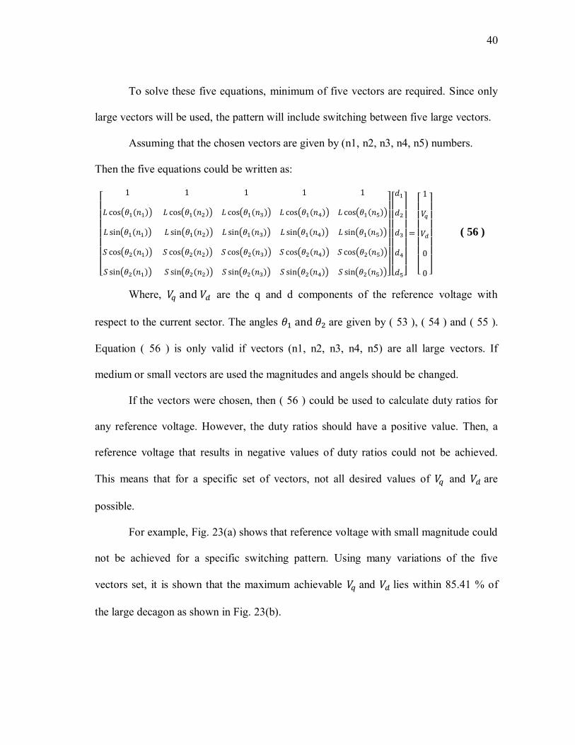
To solve these five equations, minimum of five vectors are required. Since only
large vectors will be used, the pattern will include switching between five large vectors.
Assuming that the chosen vectors are given by (n1, n2, n3, n4, n5) numbers.
Then the five equations could be written as:
[
( ( )) ( ( )) ( ( )) ( ( )) ( ( ))
( ( )) ( ( )) ( ( )) ( ( )) ( ( ))
( ( )) ( ( )) ( ( )) ( ( )) ( ( ))
( ( )) ( ( )) ( ( )) ( ( )) ( ( ))]
[
]
[
]
( 56 )
Where, are the q and d components of the reference voltage with
respect to the current sector. The angles are given by ( 53 ), ( 54 ) and ( 55 ).
Equation ( 56 ) is only valid if vectors (n1, n2, n3, n4, n5) are all large vectors. If
medium or small vectors are used the magnitudes and angels should be changed.
If the vectors were chosen, then ( 56 ) could be used to calculate duty ratios for
any reference voltage. However, the duty ratios should have a positive value. Then, a
reference voltage that results in negative values of duty ratios could not be achieved.
This means that for a specific set of vectors, not all desired values of and are
possible.
For example, Fig. 23(a) shows that reference voltage with small magnitude could
not be achieved for a specific switching pattern. Using many variations of the five
vectors set, it is shown that the maximum achievable and lies within 85.41 % of
the large decagon as shown in Fig. 23(b).
41
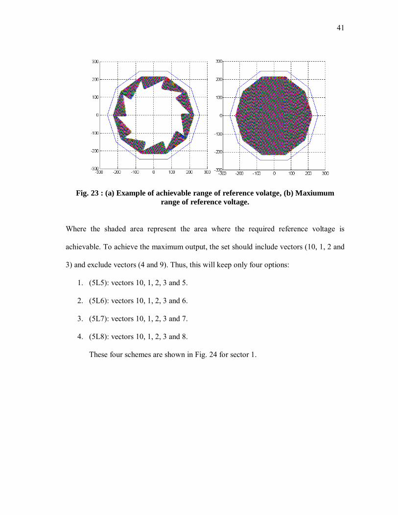
Fig. 23 : (a) Example of achievable range of reference volatge, (b) Maxiumum
range of reference voltage.
Where the shaded area represent the area where the required reference voltage is
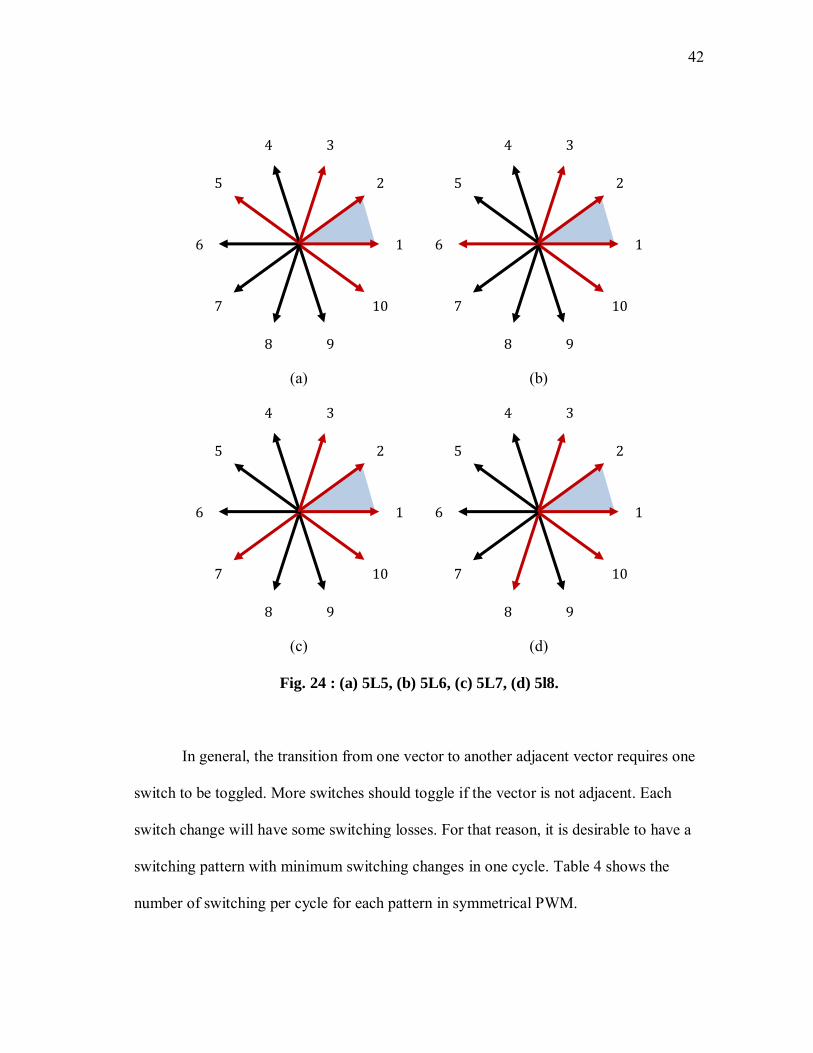
achievable. To achieve the maximum output, the set should include vectors (10, 1, 2 and
3) and exclude vectors (4 and 9). Thus, this will keep only four options:
1. (5L5): vectors 10, 1, 2, 3 and 5.
2. (5L6): vectors 10, 1, 2, 3 and 6.
3. (5L7): vectors 10, 1, 2, 3 and 7.
4. (5L8): vectors 10, 1, 2, 3 and 8.
These four schemes are shown in Fig. 24 for sector 1.
42
(a) (b)
(c) (d)
Fig. 24 : (a) 5L5, (b) 5L6, (c) 5L7, (d) 5l8.
In general, the transition from one vector to another adjacent vector requires one
switch to be toggled. More switches should toggle if the vector is not adjacent. Each
switch change will have some switching losses. For that reason, it is desirable to have a
switching pattern with minimum switching changes in one cycle. Table 4 shows the
number of switching per cycle for each pattern in symmetrical PWM.
9
10
1
2
3 4
5
6
7
8 9
10
1
2
3 4
5
6
7
8
9
10
1
2
3 4
5
6
7
8 9
10
1
2
3 4
5
6
7
8

43
Table 4 : Number of switchings (5L)
Number of switchings
5L5 5 5L6 6 5L7 6 5L8 5
To compare the performance of the four sets, these sets were simulated in an
open loop system and the total harmonic distortion THD is shown in Table 5.
Table 5 : Total harmonic distortion (5L)
No load Loaded
5L5 20.05 % 17.86 % 5L6 12.89 % 11.39 % 5L7 14.96 % 13.32 % 5L8 18.71 % 16.84 %
It is clear from the table above that the set (5L6) will have the less current THD
for both loaded and unloaded case. Thus, among the 5 large vectors schemes, (5L6)
represents the best option. In the next section, this switching scheme is implemented.
Moreover, 5L8 shows better performance compared to 5L5 with the same
switching losses. For that reason, 5L8 will also be implemented.
44
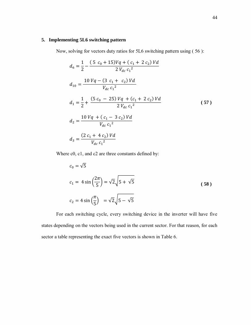
5. Implementing 5L6 switching pattern
Now, solving for vectors duty ratios for 5L6 switching pattern using ( 56 ):
( ) ( )
( )
( ) ( )
( )
( )
( 57 )
Where c0, c1, and c2 are three constants defined by:
√
(
) √ √ √
(
) √ √ √
( 58 )
For each switching cycle, every switching device in the inverter will have five
states depending on the vectors being used in the current sector. For that reason, for each
sector a table representing the exact five vectors is shown in Table 6.

45
Table 6 : 5L6 switching pattern for each sector Vector Numbers 6 3 2 1 10 T1 T2
Sector 1
Values 6 19 17 25 24 S1 0 1 1 1 1 d1 1 S2 0 0 0 1 1 d1+d2+d3 1 S3 1 0 0 0 0 0 d1 S4 1 1 0 0 0 0 d1+d2 S5 0 1 1 1 0 d1 d1+d2+d3+d4
Sector 2
Values 14 3 19 17 25 S1 0 0 1 1 1 d1+d2 1 S2 1 0 0 0 1 d1 d1+d2+d3+d4 S3 1 0 0 0 0 0 d1 S4 1 1 1 0 0 0 d1+d2+d3 S5 0 1 1 1 1 d1 1
Sector 3
Values 12 7 3 19 17 S1 0 0 0 1 1 d1+d2+d3 1 S2 1 0 0 0 0 0 d1 S3 1 1 0 0 0 0 d1+d2 S4 0 1 1 1 0 d1 d1+d2+d3+d4 S5 0 1 1 1 1 d1 1
Sector 4
Values 28 6 7 3 19 S1 1 0 0 0 1 d1 d1+d2+d3+d4 S2 1 0 0 0 0 0 d1 S3 1 1 1 0 0 0 d1+d2+d3 S4 0 1 1 1 1 d1 1 S5 0 0 1 1 1 d1+d2 1
Sector 5
Values 24 14 6 7 3 S1 1 0 0 0 0 0 d1 S2 1 1 0 0 0 0 d1+d2 S3 0 1 1 1 0 d1 d1+d2+d3+d4 S4 0 1 1 1 1 d1 1 S5 0 0 0 1 1 d1+d2+d3 1
Sector 6
Values 25 12 14 6 7 S1 1 0 0 0 0 0 d1 S2 1 1 1 0 0 0 d1+d2+d3 S3 0 1 1 1 1 d1 1 S4 0 0 1 1 1 d1+d2 1 S5 1 0 0 0 1 d1 d1+d2+d3+d4
Sector 7
Values 17 28 12 14 6 S1 1 1 0 0 0 0 d1+d2 S2 0 1 1 1 0 d1 d1+d2+d3+d4 S3 0 1 1 1 1 d1 1 S4 0 0 0 1 1 d1+d2+d3 1 S5 1 0 0 0 0 0 d1
Sector 8
Values 19 24 28 12 14 S1 1 1 1 0 0 0 d1+d2+d3 S2 0 1 1 1 1 d1 1 S3 0 0 1 1 1 d1+d2 1 S4 1 0 0 0 1 d1 d1+d2+d3+d4 S5 1 0 0 0 0 0 d1
Sector 9
Values 3 25 24 28 12 S1 0 1 1 1 0 d1 d1+d2+d3+d4 S2 0 1 1 1 1 d1 1 S3 0 0 0 1 1 d1+d2+d3 1 S4 1 0 0 0 0 0 d1 S5 1 1 0 0 0 0 d1+d2
Sector 10
Values 7 17 25 24 28 S1 0 1 1 1 1 d1 1 S2 0 0 1 1 1 d1+d2 1 S3 1 0 0 0 1 d1 d1+d2+d3+d4 S4 1 0 0 0 0 0 d1 S5 1 1 1 0 0 0 d1+d2+d3

46
To implement the system, two parameters and should be defined for each
switch (S1, S2, S3, S4 and S5). As shown in Fig. 25, is the time to switch ON and
represent the offset while is the Time to switch OFF.
Fig. 25 : Switching Cycle (Mode 1)
As shown in Table 6, in some cases we will have two pulses in one cycle. These
cases are marked in red. To implement these cases, the switching control should change
such that the first pulse start at zero and ends at . The second pulse will start at and
end at the end of the period as shown in Fig. 26:
Fig. 26 : Switching Cycle (Mode 2)
𝑇
𝑇
𝑇𝑠
𝑇
𝑇
𝑇𝑠
47
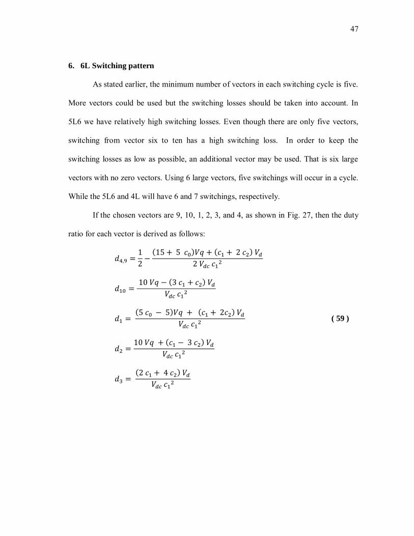
6. 6L Switching pattern
As stated earlier, the minimum number of vectors in each switching cycle is five.
More vectors could be used but the switching losses should be taken into account. In
5L6 we have relatively high switching losses. Even though there are only five vectors,
switching from vector six to ten has a high switching loss. In order to keep the
switching losses as low as possible, an additional vector may be used. That is six large
vectors with no zero vectors. Using 6 large vectors, five switchings will occur in a cycle.
While the 5L6 and 4L will have 6 and 7 switchings, respectively.
If the chosen vectors are 9, 10, 1, 2, 3, and 4, as shown in Fig. 27, then the duty
ratio for each vector is derived as follows:
( ) ( )
( )
( ) ( )
( )
( )
( 59 )
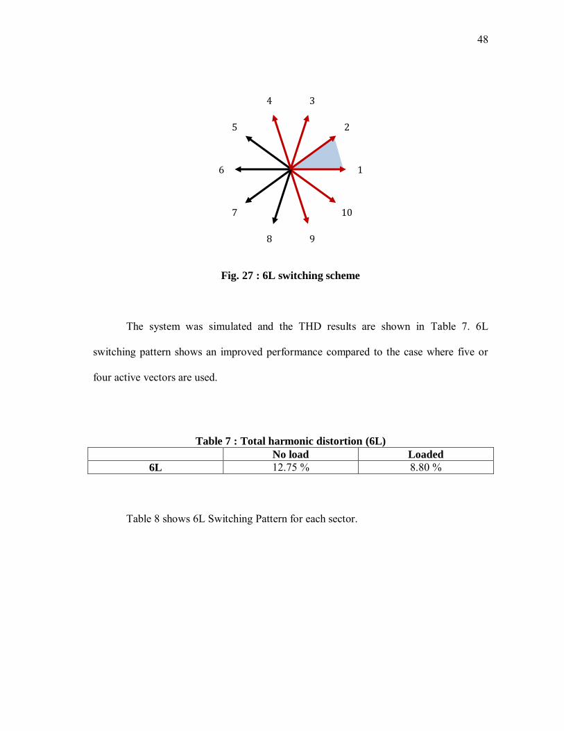
48
Fig. 27 : 6L switching scheme
The system was simulated and the THD results are shown in Table 7. 6L
switching pattern shows an improved performance compared to the case where five or
four active vectors are used.
Table 7 : Total harmonic distortion (6L)
No load Loaded
6L 12.75 % 8.80 %
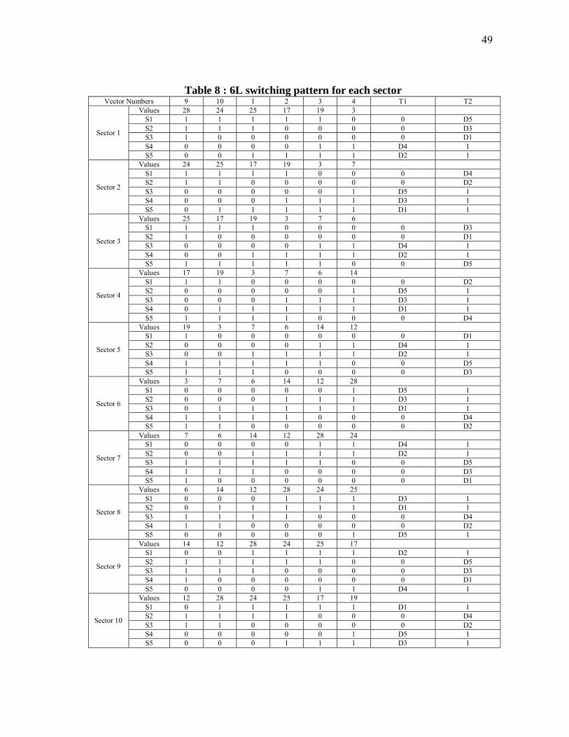
Table 8 shows 6L Switching Pattern for each sector.
9
10
1
2
3 4
5
6
7
8
49
Table 8 : 6L switching pattern for each sector Vector Numbers 9 10 1 2 3 4 T1 T2
Sector 1
Values 28 24 25 17 19 3 S1 1 1 1 1 1 0 0 D5 S2 1 1 1 0 0 0 0 D3 S3 1 0 0 0 0 0 0 D1 S4 0 0 0 0 1 1 D4 1 S5 0 0 1 1 1 1 D2 1
Sector 2
Values 24 25 17 19 3 7 S1 1 1 1 1 0 0 0 D4 S2 1 1 0 0 0 0 0 D2 S3 0 0 0 0 0 1 D5 1 S4 0 0 0 1 1 1 D3 1 S5 0 1 1 1 1 1 D1 1
Sector 3
Values 25 17 19 3 7 6 S1 1 1 1 0 0 0 0 D3 S2 1 0 0 0 0 0 0 D1 S3 0 0 0 0 1 1 D4 1 S4 0 0 1 1 1 1 D2 1 S5 1 1 1 1 1 0 0 D5
Sector 4
Values 17 19 3 7 6 14 S1 1 1 0 0 0 0 0 D2 S2 0 0 0 0 0 1 D5 1 S3 0 0 0 1 1 1 D3 1 S4 0 1 1 1 1 1 D1 1 S5 1 1 1 1 0 0 0 D4
Sector 5
Values 19 3 7 6 14 12 S1 1 0 0 0 0 0 0 D1 S2 0 0 0 0 1 1 D4 1 S3 0 0 1 1 1 1 D2 1 S4 1 1 1 1 1 0 0 D5 S5 1 1 1 0 0 0 0 D3
Sector 6
Values 3 7 6 14 12 28 S1 0 0 0 0 0 1 D5 1 S2 0 0 0 1 1 1 D3 1 S3 0 1 1 1 1 1 D1 1 S4 1 1 1 1 0 0 0 D4 S5 1 1 0 0 0 0 0 D2
Sector 7
Values 7 6 14 12 28 24 S1 0 0 0 0 1 1 D4 1 S2 0 0 1 1 1 1 D2 1 S3 1 1 1 1 1 0 0 D5 S4 1 1 1 0 0 0 0 D3 S5 1 0 0 0 0 0 0 D1
Sector 8
Values 6 14 12 28 24 25 S1 0 0 0 1 1 1 D3 1 S2 0 1 1 1 1 1 D1 1 S3 1 1 1 1 0 0 0 D4 S4 1 1 0 0 0 0 0 D2 S5 0 0 0 0 0 1 D5 1
Sector 9
Values 14 12 28 24 25 17 S1 0 0 1 1 1 1 D2 1 S2 1 1 1 1 1 0 0 D5 S3 1 1 1 0 0 0 0 D3 S4 1 0 0 0 0 0 0 D1 S5 0 0 0 0 1 1 D4 1
Sector 10
Values 12 28 24 25 17 19 S1 0 1 1 1 1 1 D1 1 S2 1 1 1 1 0 0 0 D4 S3 1 1 0 0 0 0 0 D2 S4 0 0 0 0 0 1 D5 1 S5 0 0 0 1 1 1 D3 1

50
CHAPTER V
ZERO SEQUENCE CIRCUIT
1. Introduction
In most drive systems, be they three-phase or five-phase, the dc bus is floating.
That is, there is no connection between the dc bus terminals and earth. In this case, the
dc bus is produced from a rectifier as shown in Fig. 28. The voltage between point o and
ground has a low magnitude and low frequency compared to the inverter voltages.
Thus, it will have no effect on the high frequency circuit. For that reason, is
neglected and the common mode voltages is referenced to ground instead of point o.
Fig. 28 : Motor drive system
The model of the whole system including the voltage source inverter, the stator
windings, and the impedance to ground could be represented by,
51
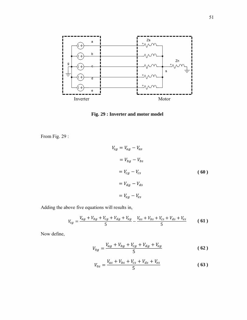
Fig. 29 : Inverter and motor model
From Fig. 29 :
( 60 )
Adding the above five equations will results in,
( 61 )
Now define,
( 62 )
( 63 )
Inverter Motor
52
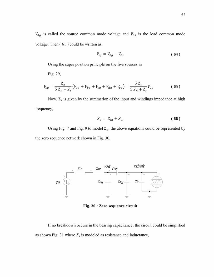
is called the source common mode voltage and is the load common mode
voltage. Then ( 61 ) could be written as,
( 64 )
Using the super position principle on the five sources in
Fig. 29,
( )
( 65 )
Now, is given by the summation of the input and windings impedance at high
frequency,
( 66 )
Using Fig. 7 and Fig. 9 to model , the above equations could be represented by
the zero sequence network shown in Fig. 30,
Fig. 30 : Zero sequence circuit
If no breakdown occurs in the bearing capacitance, the circuit could be simplified
as shown Fig. 31 where is modeled as resistance and inductance,
g h
53
Fig. 31 : Simplified zero sequence circuit
Where C is the equivalent capacitance of the system given by:
( )
( 67 )
The zero sequence circuit could be used to write the qd0 transformation of the
load voltage
in terms of the abc source voltage rather than the abc load
voltage . Using the qd0 transformation:
( ) ( )
[ ]
( ) ( )
[ ]
Since the summation of the first four rows of ( ) is zero, then the term
could be removed.
( )
[
]
( 68 )
Where is given by the zero sequence circuit as,
54
( 69 )
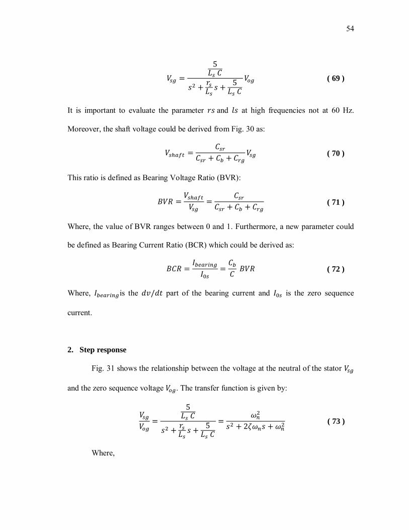
It is important to evaluate the parameter and at high frequencies not at 60 Hz.
Moreover, the shaft voltage could be derived from Fig. 30 as:
( 70 )
This ratio is defined as Bearing Voltage Ratio (BVR):
( 71 )
Where, the value of BVR ranges between 0 and 1. Furthermore, a new parameter could
be defined as Bearing Current Ratio (BCR) which could be derived as:
( 72 )
Where, is the part of the bearing current and is the zero sequence
current.
2. Step response
Fig. 31 shows the relationship between the voltage at the neutral of the stator
and the zero sequence voltage . The transfer function is given by:
( 73 )
Where,
55
√
√
( 74 )
The step response could be derived to be:
( ) √ ( (
)) ( 75 )
The constants A and B depends on the initial conditions ( ) and ( )
( )
( )
( ( ) )
( 76 )
If the initial condition were set to zero, B will be very small with respect to A.
Then the response could be approximated as:
( ) ( ( )) ( 77 )
Since only large vectors are used, is limited between two values only
as
shown in Table 2. This means that the input of the system will be a positive or negative
step with a constant magnitude.
Whenever the input switches to
, there will be some negative initial
condition. Fig. 32 shows the step response for different initial conditions.

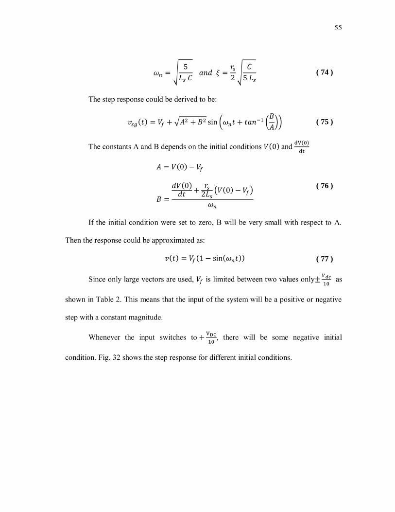
56
Fig. 32 : Step Response (a) with zero intial condition (b) intial condition = -1
For different motors, the parameters are different. Thus, the switching frequency
and damping are dependent on the motor. If the switching frequency is low or the
damping is high, the next switching will occur when the response is settled to its final
value. Thus, the next switching will start with a negative
as an initial value.
3. Special case
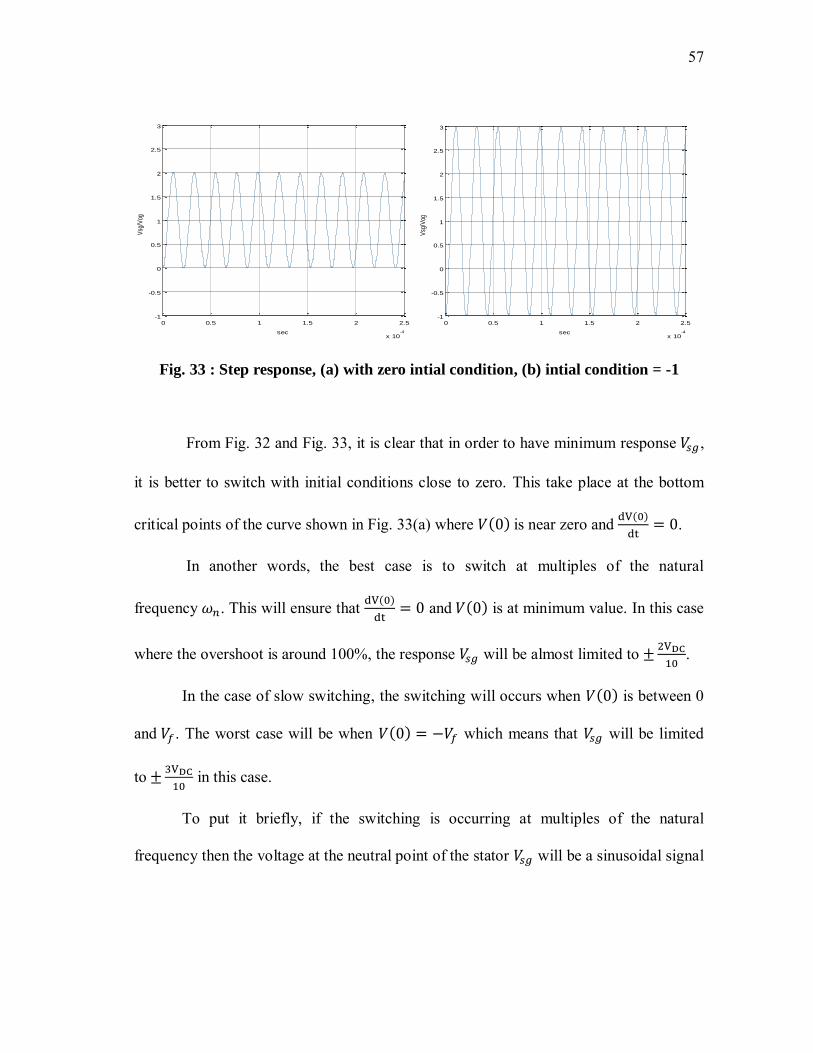
If the switching frequency is high or damping is very low, the system will appear
as an almost undamped system as shown in Fig. 33.
0 0.05 0.1 0.15 0.2 0.25-1
-0.5
0
0.5
1
1.5
2
2.5
3
sec
Vsg
/Vog
0 0.05 0.1 0.15 0.2 0.25-1
-0.5
0
0.5
1
1.5
2
2.5
3
sec
Vsg
/Vog
57
Fig. 33 : Step response, (a) with zero intial condition, (b) intial condition = -1
From Fig. 32 and Fig. 33, it is clear that in order to have minimum response ,
it is better to switch with initial conditions close to zero. This take place at the bottom
critical points of the curve shown in Fig. 33(a) where ( ) is near zero and ( )
.
In another words, the best case is to switch at multiples of the natural
frequency . This will ensure that ( )
and ( ) is at minimum value. In this case
where the overshoot is around 100%, the response will be almost limited to
.
In the case of slow switching, the switching will occurs when ( ) is between 0
and . The worst case will be when ( ) which means that will be limited
to
in this case.
To put it briefly, if the switching is occurring at multiples of the natural
frequency then the voltage at the neutral point of the stator will be a sinusoidal signal
0 0.5 1 1.5 2 2.5
x 10-4
-1
-0.5
0
0.5
1
1.5
2
2.5
3
sec
Vsg
/Vog
0 0.5 1 1.5 2 2.5
x 10-4
-1
-0.5
0
0.5
1
1.5
2
2.5
3
sec
Vsg
/Vog

58
with frequency equals the natural frequency of the system and amplitude limited
between
and
depending on the switching frequency.
To switch at multiples of the natural frequency, the switching frequency should
be set to:
( 78 )
Where n is an integer.
Moreover, the actual switching is not occurring at only. Because at each
switching period, the inverter is switching between five vectors each with specific duty
ratio. For that reason, the duty ratios should be set to specific values such that no
switching occurs at a fraction of the natural frequency.
If the desired minimum duty ratio is given by the following frequency:
( 79 )
Then, after the calculations of the duty ratio values, each value should be
rounded to the nearest 1/m value while keeping the sum of the duty ratios equals to one.
59
CHAPTER VI
SIMULATIONS AND EXPERIMENTAL RESULTS
1. Obtaining zero sequence circuit parameters’ values
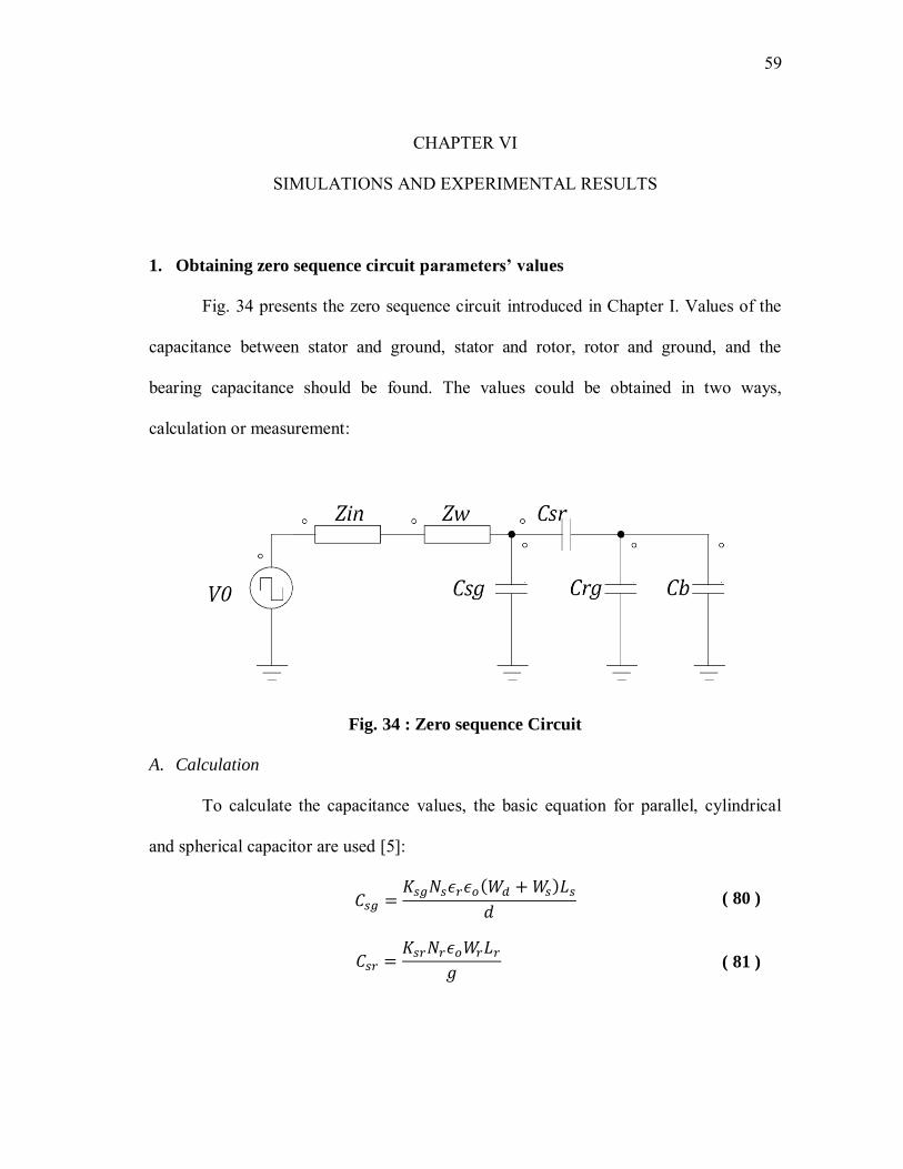
Fig. 34 presents the zero sequence circuit introduced in Chapter I. Values of the
capacitance between stator and ground, stator and rotor, rotor and ground, and the
bearing capacitance should be found. The values could be obtained in two ways,
calculation or measurement:
Fig. 34 : Zero sequence Circuit
A. Calculation
To calculate the capacitance values, the basic equation for parallel, cylindrical
and spherical capacitor are used [5]:
( )
( 80 )
( 81 )

60
(
)
( 82 )
(
)
( 83 )
Where,
is the number of stator slots.
is the number of rotor slots.
is the number of balls.
is the relative permittivity.
is the depth of the stator slots.
is the width of the stator slots.
is the width of the rotor conductor.
is the length of the stator.
is the length of the rotor.
g is the air gap.
d is the slot paper thickness.
is the inside radius of stator.
is the outer radius of the rotor.
is the radius of the ball.
is the radial clearance.
61
B. Measuring
Measuring the capacitances could be made using an LCR meter. To measure
the rotor should be removed to eliminate the effects of other capacitance. is
measured by grounding the shaft. After that, the value of is subtracted from the
measured reading. To measure , the impedance from rotor to frame is measured, then
the effects of , and are subtracted [5].
The results obtained are shown in the following Table.
Table 9 : Parameter values
Measured Value 6.498 nF 0.042 nF 1.372 nF 0.350 nF
For these values the expected Bearing Voltage Ratio is:
( 84 )
This indicates that the shaft voltage is expected to be 2.38% of the stator neutral
voltage. If zero vectors are used in the switching pattern, the stator neutral voltage will
vary between
. While if no zero vectors were used it will be between
. The
shaft voltage will equal the BVR times this voltages.

62
Next, the circuit is simulated with two cases; with or without zero vectors. For
each case, different switching schemes are implemented. The results are shown in the
next sections along with the experimental results.
2. Simulation results
The zero sequence circuit was used in the simulation. All the previously
mentioned switching schemes were simulated. These include 2L, 2L+2M, 4L, 5L8, 5L6,
6L. The results are shown for both loaded and unloaded cases.
First, the line currents were compared. Table 10 shows the total harmonic
distortion THD in line current for these switching schemes.
Table 10 : THD for various switching scheme (simulation)
No load Loaded
2L 322.2 % 215.8 % 2L+2M 17.48 % 11.74 %
4L 15.20 % 10.23 % 5L6 12.89 % 11.39 % 5L8 18.71 % 16.84 % 6L 12.75 % 8.80 %
Moreover, the neutral point voltage, neutral point current, shaft voltage and
bearing current are shown in the following figures for all switching patterns. These
results are independent of the motor loading.
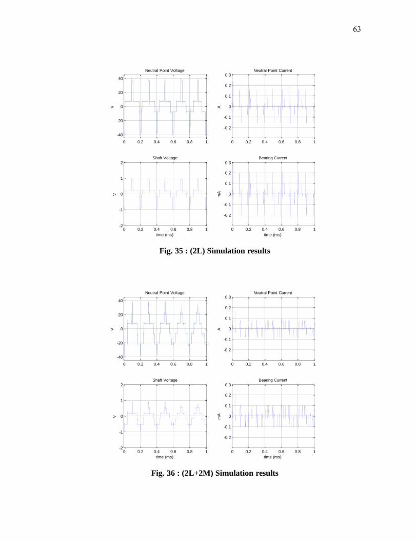
63
Fig. 35 : (2L) Simulation results
Fig. 36 : (2L+2M) Simulation results
0 0.2 0.4 0.6 0.8 1
-40
-20
0
20
40
Neutral Point Voltage
V
0 0.2 0.4 0.6 0.8 1
-0.2
-0.1
0
0.1
0.2
0.3Neutral Point Current
A
0 0.2 0.4 0.6 0.8 1-2
-1
0
1
2Shaft Voltage
V
time (ms)
0 0.2 0.4 0.6 0.8 1
-0.2
-0.1
0
0.1
0.2
0.3Bearing Current
mA
time (ms)
0 0.2 0.4 0.6 0.8 1
-40
-20
0
20
40
Neutral Point Voltage
V
0 0.2 0.4 0.6 0.8 1
-0.2
-0.1
0
0.1
0.2
0.3Neutral Point Current
A
0 0.2 0.4 0.6 0.8 1-2
-1
0
1
2Shaft Voltage
V
time (ms)
0 0.2 0.4 0.6 0.8 1
-0.2
-0.1
0
0.1
0.2
0.3Bearing Current
mA
time (ms)
64
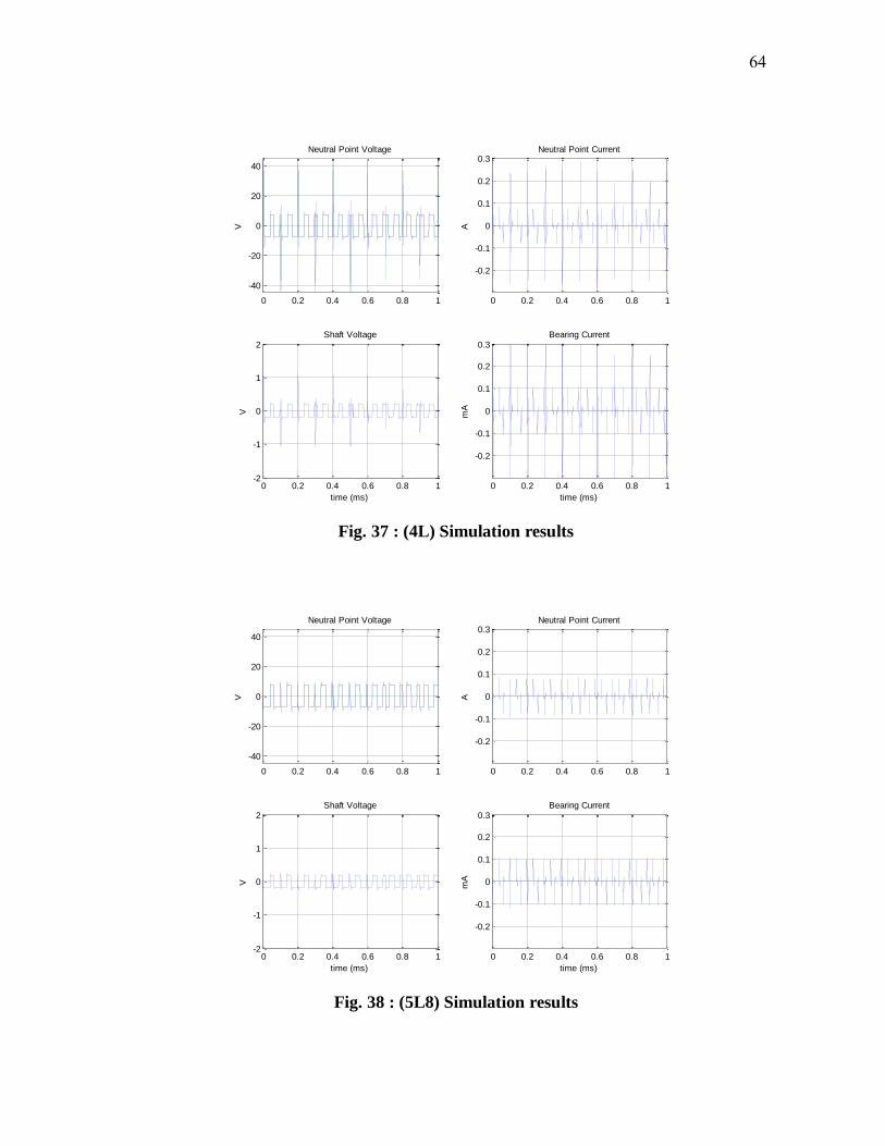
Fig. 37 : (4L) Simulation results
Fig. 38 : (5L8) Simulation results
0 0.2 0.4 0.6 0.8 1
-40
-20
0
20
40
Neutral Point Voltage
V
0 0.2 0.4 0.6 0.8 1
-0.2
-0.1
0
0.1
0.2
0.3Neutral Point Current
A
0 0.2 0.4 0.6 0.8 1-2
-1
0
1
2Shaft Voltage
V
time (ms)
0 0.2 0.4 0.6 0.8 1
-0.2
-0.1
0
0.1
0.2
0.3Bearing Current
mA
time (ms)
0 0.2 0.4 0.6 0.8 1
-40
-20
0
20
40
Neutral Point Voltage
V
0 0.2 0.4 0.6 0.8 1
-0.2
-0.1
0
0.1
0.2
0.3Neutral Point Current
A
0 0.2 0.4 0.6 0.8 1-2
-1
0
1
2Shaft Voltage
V
time (ms)
0 0.2 0.4 0.6 0.8 1
-0.2
-0.1
0
0.1
0.2
0.3Bearing Current
mA
time (ms)
65
Fig. 39 : (5L6) Simulation results
Fig. 40 : (6L) Simulation results
0 0.2 0.4 0.6 0.8 1
-40
-20
0
20
40
Neutral Point Voltage
V
0 0.2 0.4 0.6 0.8 1
-0.2
-0.1
0
0.1
0.2
0.3Neutral Point Current
A
0 0.2 0.4 0.6 0.8 1-2
-1
0
1
2Shaft Voltage
V
time (ms)
0 0.2 0.4 0.6 0.8 1
-0.2
-0.1
0
0.1
0.2
0.3Bearing Current
mA
time (ms)
0 0.2 0.4 0.6 0.8 1
-40
-20
0
20
40
Neutral Point Voltage
V
0 0.2 0.4 0.6 0.8 1
-0.2
-0.1
0
0.1
0.2
0.3Neutral Point Current
A
0 0.2 0.4 0.6 0.8 1-2
-1
0
1
2Shaft Voltage
V
time (ms)
0 0.2 0.4 0.6 0.8 1
-0.2
-0.1
0
0.1
0.2
0.3Bearing Current
mA
time (ms)
66
Since the shaft voltage is way below the break down voltage, the current in the
previous figures represent only the part of the bearing current not the EDM part.
bearing current does not depend on the magnitude of the shaft voltage but on the
rate of change of it. In all switching schemes except 4L the voltage changes in
steps.
Therefore, they will have the same bearing current. 4L have voltage steps of
and
thus has a higher bearing current.
The main advantage of 6L compared to 2L+2M is improving the THD while
decreasing the shaft voltage. This will keep the bearing current at the same level
while decrease the opportunity of EDM bearing currents.
The above results show that the peak value of shaft voltage in 6L is reduced by 5
times as expected. Furthermore, when the zero vectors were used, the rms shaft voltage
was 0.872 V while when only large vectors where used it was reduced to 0.193 V. The
expected BVR in the simulation is 2.38 %.
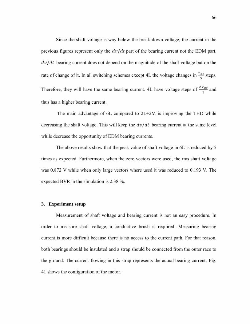
3. Experiment setup
Measurement of shaft voltage and bearing current is not an easy procedure. In
order to measure shaft voltage, a conductive brush is required. Measuring bearing
current is more difficult because there is no access to the current path. For that reason,
both bearings should be insulated and a strap should be connected from the outer race to
the ground. The current flowing in this strap represents the actual bearing current. Fig.
41 shows the configuration of the motor.
67
Fig. 41 : Motor configuration.
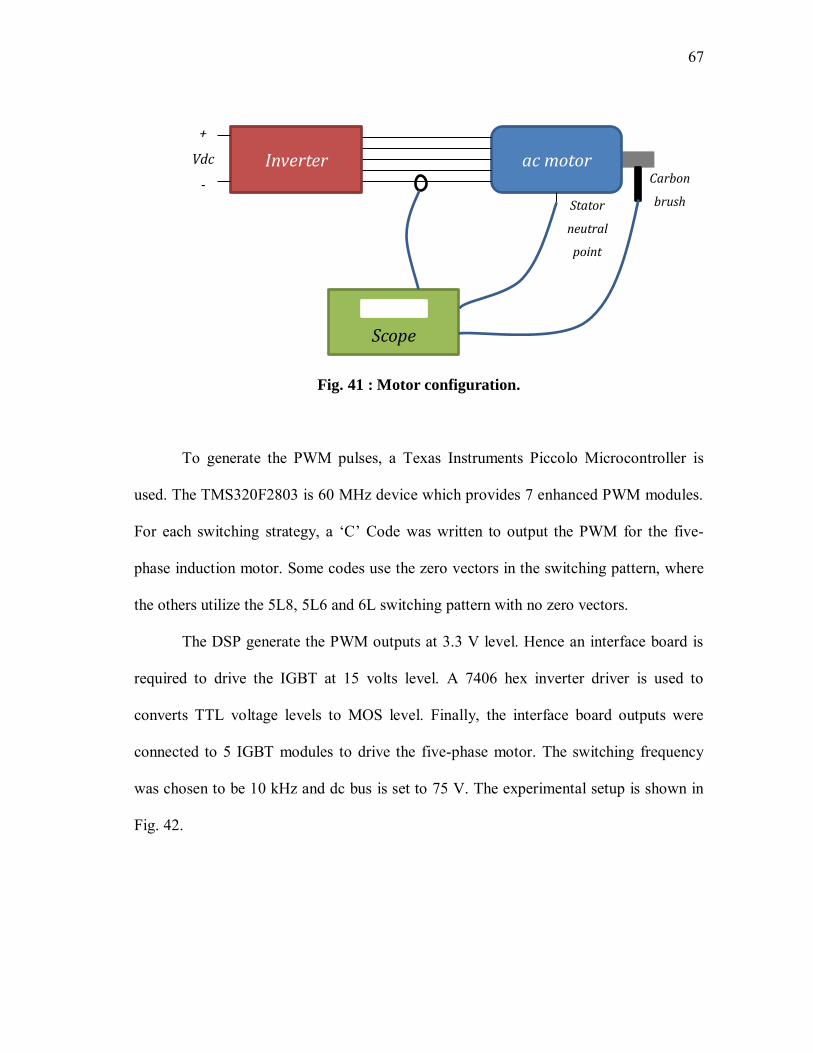
To generate the PWM pulses, a Texas Instruments Piccolo Microcontroller is
used. The TMS320F2803 is 60 MHz device which provides 7 enhanced PWM modules.
For each switching strategy, a ‘C’ Code was written to output the PWM for the five-
phase induction motor. Some codes use the zero vectors in the switching pattern, where
the others utilize the 5L8, 5L6 and 6L switching pattern with no zero vectors.
The DSP generate the PWM outputs at 3.3 V level. Hence an interface board is
required to drive the IGBT at 15 volts level. A 7406 hex inverter driver is used to
converts TTL voltage levels to MOS level. Finally, the interface board outputs were
connected to 5 IGBT modules to drive the five-phase motor. The switching frequency
was chosen to be 10 kHz and dc bus is set to 75 V. The experimental setup is shown in
Fig. 42.
ac motor
Scope
Inverter
+
Vdc
-
Carbon
brush Stator
neutral
point
68
Fig. 42 : Experiment setup
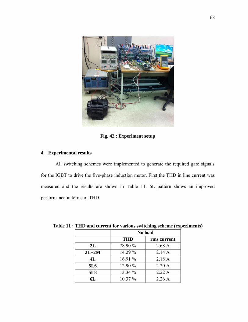
4. Experimental results
All switching schemes were implemented to generate the required gate signals
for the IGBT to drive the five-phase induction motor. First the THD in line current was
measured and the results are shown in Table 11. 6L pattern shows an improved
performance in terms of THD.
Table 11 : THD and current for various switching scheme (experiments)
No load
THD rms current
2L 78.90 % 2.68 A 2L+2M 14.29 % 2.14 A
4L 16.91 % 2.18 A 5L6 12.90 % 2.20 A 5L8 13.34 % 2.22 A 6L 10.37 % 2.26 A
69
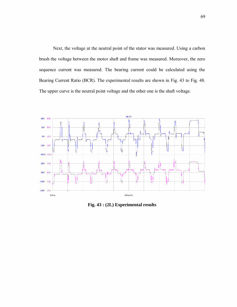
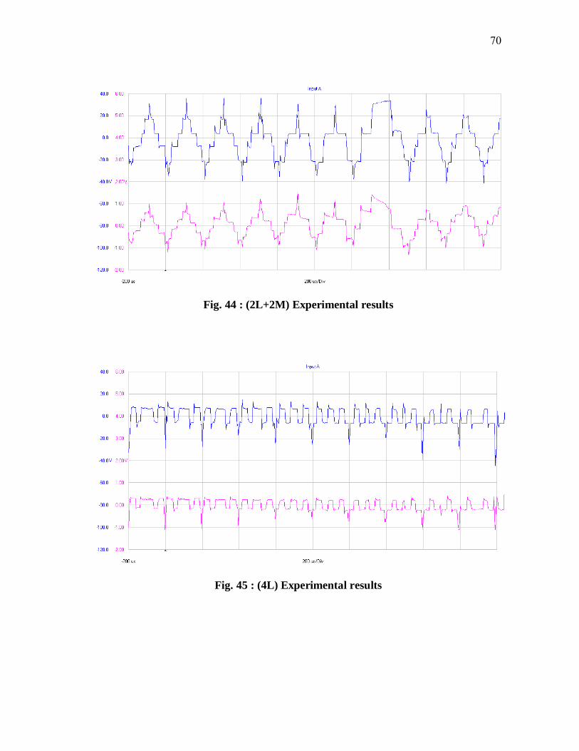
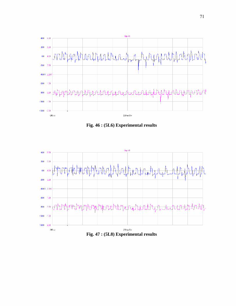
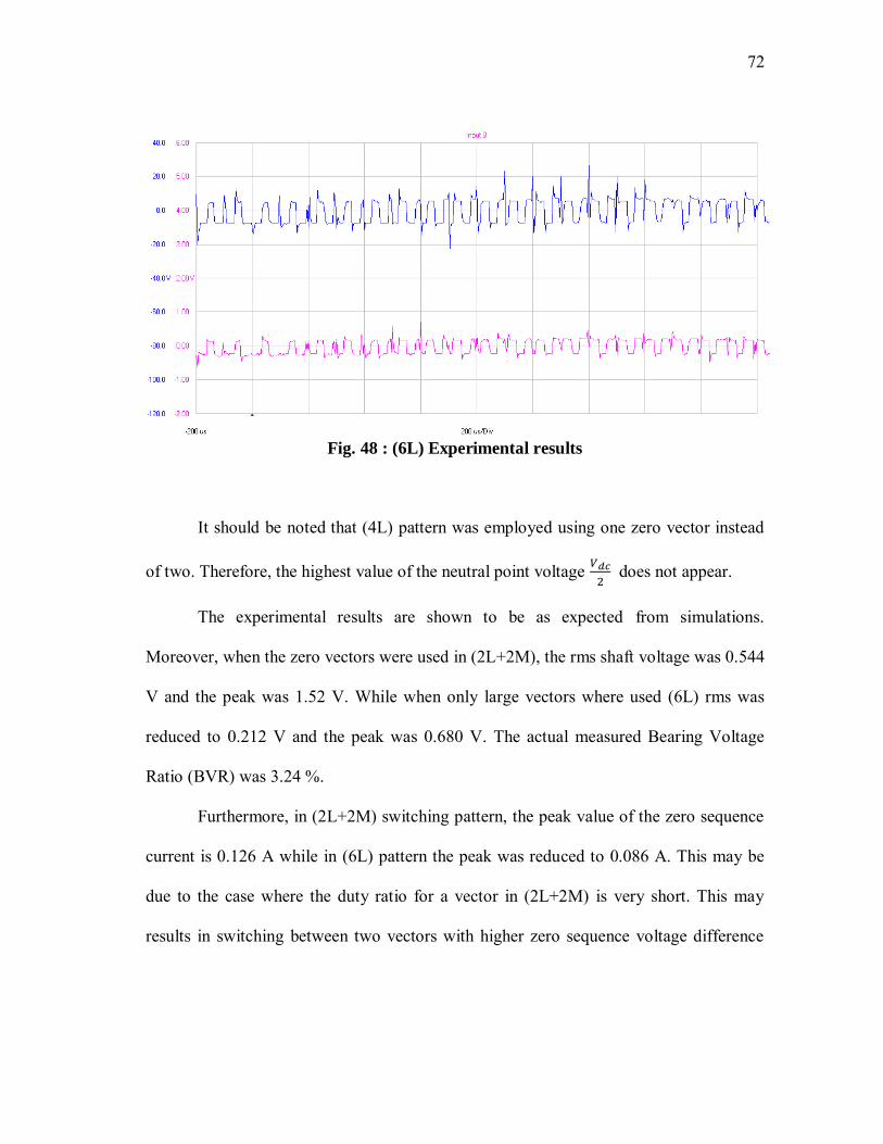
Next, the voltage at the neutral point of the stator was measured. Using a carbon
brush the voltage between the motor shaft and frame was measured. Moreover, the zero
sequence current was measured. The bearing current could be calculated using the
Bearing Current Ratio (BCR). The experimental results are shown in Fig. 43 to Fig. 48.
The upper curve is the neutral point voltage and the other one is the shaft voltage.
Fig. 43 : (2L) Experimental results
70
Fig. 44 : (2L+2M) Experimental results
Fig. 45 : (4L) Experimental results
71
Fig. 46 : (5L6) Experimental results
Fig. 47 : (5L8) Experimental results
72
Fig. 48 : (6L) Experimental results
It should be noted that (4L) pattern was employed using one zero vector instead
of two. Therefore, the highest value of the neutral point voltage
does not appear.
The experimental results are shown to be as expected from simulations.
Moreover, when the zero vectors were used in (2L+2M), the rms shaft voltage was 0.544
V and the peak was 1.52 V. While when only large vectors where used (6L) rms was
reduced to 0.212 V and the peak was 0.680 V. The actual measured Bearing Voltage
Ratio (BVR) was 3.24 %.
Furthermore, in (2L+2M) switching pattern, the peak value of the zero sequence
current is 0.126 A while in (6L) pattern the peak was reduced to 0.086 A. This may be
due to the case where the duty ratio for a vector in (2L+2M) is very short. This may
results in switching between two vectors with higher zero sequence voltage difference
73
which leads to higher . This is not the case in (6L) since all vectors have zero
sequence voltage between ⁄ and ⁄ .
Finally, (6L) switching scheme was proven to reduce the shaft voltage to 20% of
the original value. Depending on the system voltage levels and the break down voltage,
this may eliminate the EDM bearing currents.
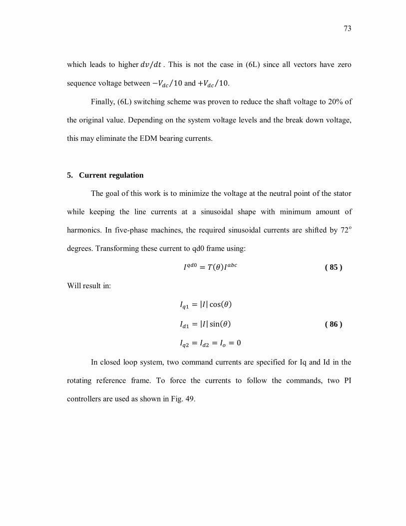
5. Current regulation
The goal of this work is to minimize the voltage at the neutral point of the stator
while keeping the line currents at a sinusoidal shape with minimum amount of
harmonics. In five-phase machines, the required sinusoidal currents are shifted by 72o
degrees. Transforming these current to qd0 frame using:
( ) ( 85 )
Will result in:
| | ( )
| | ( )
( 86 )
In closed loop system, two command currents are specified for Iq and Id in the
rotating reference frame. To force the currents to follow the commands, two PI
controllers are used as shown in Fig. 49.
74
Fig. 49 : Current Regulated SVPWM
In this system, Iq2, Id2 and Io were not fed back. It is enough to set the
corresponding command voltages Vq2, Vd2 and Vo to zero. This will insure minimizing
these currents because each of them is related to its voltage by the following transfer
function as shown in Chapter IV:
( 87 )
The e2s and s2e blocks shown in Fig. 49 transform Iq and Id from the stationary
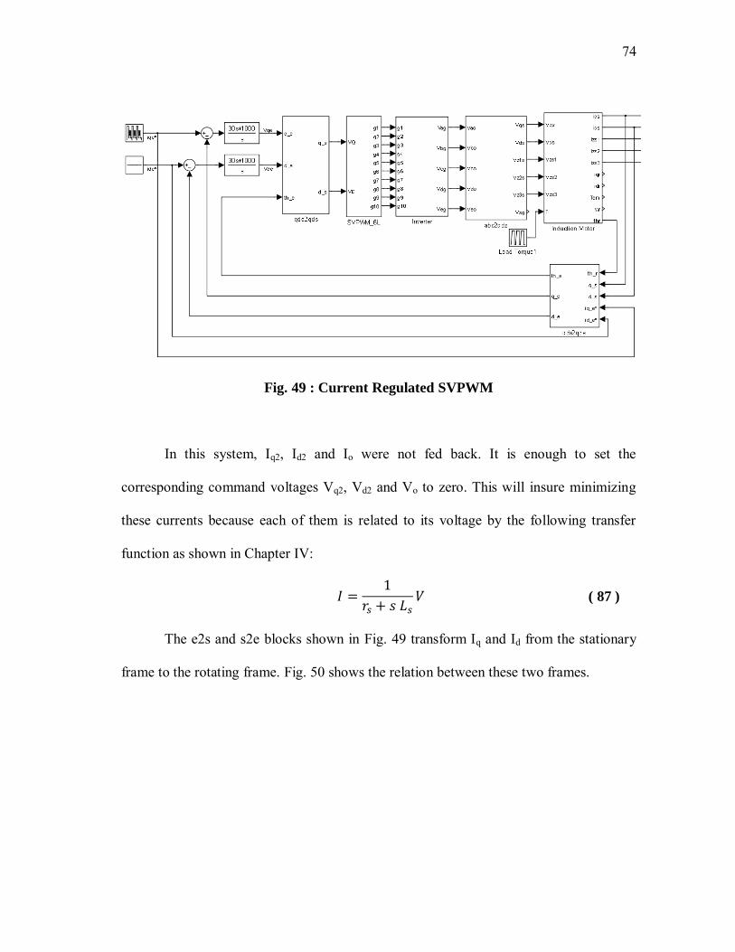
frame to the rotating frame. Fig. 50 shows the relation between these two frames.
75
Fig. 50 : Stationary and rotating refrence frames.
The angle is given by [22]:
( 88 )
( 89 )
Where is the rotor angle and is the compensated slip angle. The s2e transformation
is given by,
( ) ( )
( ) ( ) ( 90 )
Whereas e2s transformation is,
( ) ( )
( ) ( ) ( 91 )
𝜃 qs
ds de
qe
76
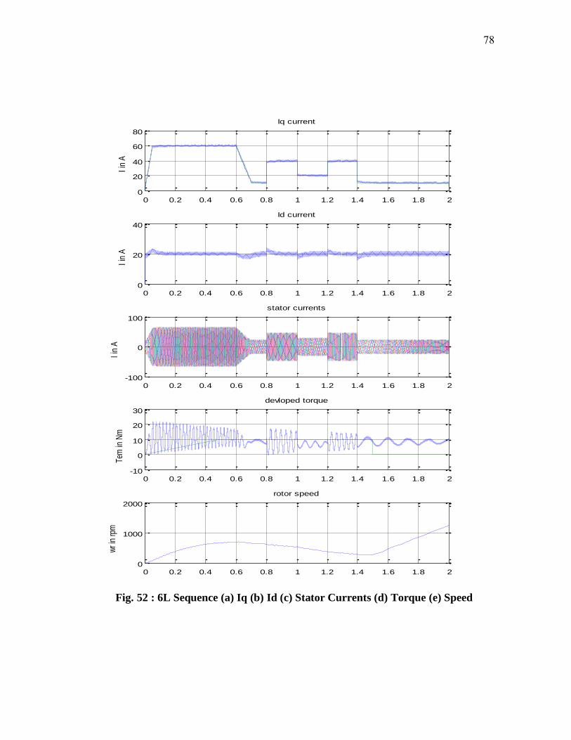
6. Comparing (6L) with (2L+2M) under CRPWM
In this section, the (6L) sequence which includes six large vectors with no zero
vectors is compared with (2L+2M) sequence which has two large, two medium and two
zero vectors. The simulation is done with Current Regulated PWM (CRPWM) to show
the ability of the new switching pattern to follow the commanded currents.
The simulation results for the (2L+2M) sequence are shown in Fig. 51. Fig. 51(a)
and (b) show Iq and Id respectively. Fig. 51(c) shows the stator currents. The torque and
speed are presented in Fig. 51(d) and (e). Similarly, Fig. 52 shows the simulation results
for (6L) sequence.
It is clear from the figures that (6L) sequence will have almost equivalent Iq, Id,
line currents, torque, speed, and THD. The only difference is that (6L) will have higher
Iq and Id current ripple. Moreover, (6L) reduces the neutral voltage and current which
will reduce the shaft voltage and bearing current.

77
Fig. 51 : 2L+2M Sequence (a) Iq (b) Id (c) Stator Currents (d) Torque (e) Speed
0 0.2 0.4 0.6 0.8 1 1.2 1.4 1.6 1.8 20
20
40
60
80
Iq currentI
in A
0 0.2 0.4 0.6 0.8 1 1.2 1.4 1.6 1.8 20
20
40
Id current
I in
A
0 0.2 0.4 0.6 0.8 1 1.2 1.4 1.6 1.8 2-100
0
100
stator currents
I in
A
0 0.2 0.4 0.6 0.8 1 1.2 1.4 1.6 1.8 2-10
0
10
20
30
devloped torque
Tem
in N
m
0 0.2 0.4 0.6 0.8 1 1.2 1.4 1.6 1.8 20
1000
2000
rotor speed
wr
in r
pm
78
Fig. 52 : 6L Sequence (a) Iq (b) Id (c) Stator Currents (d) Torque (e) Speed
0 0.2 0.4 0.6 0.8 1 1.2 1.4 1.6 1.8 20
20
40
60
80
Iq currentI i
n A
0 0.2 0.4 0.6 0.8 1 1.2 1.4 1.6 1.8 20
20
40
Id current
I in
A
0 0.2 0.4 0.6 0.8 1 1.2 1.4 1.6 1.8 2-100
0
100
stator currents
I in
A
0 0.2 0.4 0.6 0.8 1 1.2 1.4 1.6 1.8 2-10
0
10
20
30
devloped torque
Tem
in N
m
0 0.2 0.4 0.6 0.8 1 1.2 1.4 1.6 1.8 20
1000
2000
rotor speed
wr i
n rp
m
79
CHAPTER VII
CONCLUSIONS AND FUTURE WORK
Current research has a lot to say on shaft voltages and bearing currents. Many
solutions were proposed to mitigate this problem. However, all these solution include
adding cost to the system.
For five-phase induction motor, several (SVPWM) switching patterns exist. In
this thesis, a new switching pattern was developed to reduce the shaft voltages and
bearing currents. To implement the new scheme, only the software is modified and thus
there will be no additional cost.
This new pattern is compared with conventional ones. The (6L) switching
scheme was proven to reduce the shaft voltage. Depending on the system voltage levels
and the breakdown voltage, this could eliminate the EDM bearing currents.
The main advantage of (6L) compared to (2L+2M) is improving the THD.
Although, it keeps the dv/dt bearing current at the same level, it decreases the
opportunity of EDM currents.
This work could be extended to multiphase drives with more than five-phases
(e.g. seven phases) with similar switching scheme.
80
REFERENCES
[1] R. Hoppler and R. A. Errath, "Motor bearings, not just a piece of metal," in IEEE-
IAS/PCA Cement Industry Conference, North Charleston, SC, 2007.
[2] J. Erdman, R. J. Kerkman, D. Schlegel and G. Skibinski, "Effect of PWM inverters
on ac motor bearing currents and shaft voltage," in Proc. IEEE-APEC Annu.
Meeting, 1995.
[3] D. Busse, J. Erdman, R. J. Kerkman, D. Schlegel and G. Skibinski, "The effects of
PWM voltage source inverters on the mechanical performance of rolling bearings,"
in Proc. IEEE APEC ’96, San Jose, CA, 1996, pp.
[4] D. Busse, J. Erdman, R. J. Kerkman, D. Schlegel and G. Skibinski, "An evaluation
of the electrostatic shielded induction motor: a solution for rotor shaft voltage
buildup and bearing current," in Ind. Applicat.Society Conf. Rec., San Diego, CA,
1996.
[5] D. Busse, J. Erdman, R. J. Kerkman, D. Schlegel and G. Skibinski, "System
electrical parameters and their effects on bearing currents," IEEE Trans. Ind.
Applicat., vol. 33, no. 2, pp. 577-584, 1997.
[6] D. Busse, J. Erdman, R. J. Kerkman, D. Schlegel and G. Skibinski, "Bearing
currents and their relationship to PWM drives," IEEE Trans. Power Electron., vol.
12, no. 2, pp. 243-252, 1997.
[7] S. Chen, T. Lipo and D. Fitzgerald, "Source of induction motor bearing currents

81
caused by PWM inverters," IEEE Trans. Energy Convers., vol. 11, no. 1, pp. 25-32,
1996.
[8] S. Chen, T. Lipo and D. Fitzgerald, "Modeling of motor bearing currents in PWM
inverter drives," IEEE Trans. Ind. Appl., vol. 32, no. 6, pp. 1365-1370, 1996.
[9] P. Alger and H. Samson, "Shaft currents in electric machines," A.I.R.E. Conf., Feb
1924.
[10] I. Onel and M. El Hachemi Benbouzid, "Induction motor bearing failure detection
and diagnosis: park and concordia transform approaches comparative study,"
IEEE/ASME Trans. Mechatronics, vol. 13, no. 2, pp. 257-262, April 2008.
[11] A. Binder and A. Muetze, "Scaling effects of inverter-induced bearing currents in ac
machines," IEEE Trans. Ind. Applicat., vol. 44, no. 3, pp. 769 - 776, 2008.
[12] J. R. Stewart and D. D. Wilson, "High phase order transmission—a feasibility
analysis, part I—steady state considerations," IEEE Trans. Power Apparatus Syst.,
Vols. PAS-97, no. 6, p. 2300–2307, 1978.
[13] H. A. Toliyat, "Analysis and simulation of five-phase variable-speed induction
motor drives under asymmetrical connections," IEEE Trans. Power Electron., vol.
13, no. 4, pp. 748-756, 1998.
[14] A. Julian, T. Lipo and G. Oriti, "Elimination of common mode voltage in three
phase sinusoidal power converters," in PESC ’96, 1996.
[15] H. A. a. H. A. S. Ogasawara, "An active circuit for cancellation of common-mode
voltage generated by a PWM inverter," IEEE Trans. Power Electron, vol. 13, no. 5,
82
p. 835–841, 1998.
[16] . ava and . n, igh-performance PWM algorithm for common-mode voltage
reduction in three-phase voltage source inverters," IEEE Trans. Power Electron.,
vol. 26, no. 7, pp. 1998 - 2008, 2011.
[17] H. Toliyat, R. Shi and H. Xu, "A DSP-based vector control of five-phase
synchronous reluctance motor," in Conf. Rec. IEEE IAS Annu. Meeting, Rome,
Italy, 2000.
[18] A. Iqbal and E. Levi, "Space vector modulation schemes for a five-phase voltage
source inverter," in Proc. Eur. Conf. Power Elect. Appl., 2005.
[19] M. Duran and E. Levi, "Multi-dimensional approach to multi-phase space vector
pulse width modulation," in Proc. 33rd Annu. Conf. IEEE IECON, Paris, France,
2006.
[20] H.-M. Ryu, J.-H. Kim and S.-K. Sul, "Analysis of multiphase space vector pulse
width modulation based on multiple d-q spaces concept," in IPEMC Conference,
2004.
[21] S. Xue and X. Wen, "Simulation analysis of two novel multiphase SVPWM
strategies," in Proc. IEEE ICIT, Hong Kong, 2005.
[22] C.-M. Ong, "Dynamic simulations of electric machinery: using
MATLAB/SIMULINK, Prentice Hall PTR", 1998, pp. 433-440.
83
VITA
Name: Hussain A. I. A. Hussain Address: c/o Dr. Hamid A. Toliyat
Electrical Machines & Power Electronics Laboratory
Department of Electrical Engineering
TAMU 3128
Texas A&M University
College Station, Texas 77843-3128
Email Address: [email protected]
Education: B.Sc., Electrical Engineering, Kuwait University, 2007