Embed Size (px)
Citation preview

© 2017. Dr. S. S. Chorage & Miss. Mitkari Sneha U. This is a research/review paper, distributed under the terms of the Creative Commons Attribution-Noncommercial 3.0 Unported License http://creativecommons.org/licenses/by-nc/3.0/), permitting all non-commercial use, distribution, and reproduction in any medium, provided the original work is properly cited.
Reduction of Power Consumption using Different Coding Schemes using FPGA in NoC
By Dr. S. S. Chorage & Miss. Mitkari Sneha U
Abstract- Network-On-Chip (NoC) is used as a main part of a system. NoC overcomes traditional System-On-Chip (SoC) problems. Because, SoC has problems like cost, design risk, more complexity and more power consumption. In software part, Xilinx ISE Design suite 14.5 with VHDL programming is used. It is simple programming language. In hardware part, FPGA of Spartan 3E family is used. It is advanced 90nm technology. It is world’s the cheapest FPGA family. It has 500K gates and 40 LUTs. It has lowest cost per logic. Its better advantage is that it is designed for more volume-to-market. Power consumption of given system is compared with previous system. From output power analysis chart, it is concluded that given system has lower power consumption than previous system. Power consumption of gray to binary conversion block of previous system is nearly equal to power consumption of present (given) whole system. This proves that there is a great reduction in power consumption in the system.
Keywords: FPGA, LUTs, Network-on-Chip (NoC), System-on-Chip (SoC), Spartan 3E, VHDL.
GJCST-A Classification: E.4, I.4.2
ReductionofPowerConsumptionusingDifferentCodingSchemesusingFPGAinNoC
Strictly as per the compliance and regulations of:
Global Journal of Computer Science and Technology: AHardware & Computation Volume 17 Issue 1 Version 1.0 Year 2017 Type: Double Blind Peer Reviewed International Research JournalPublisher: Global Journals Inc. (USA)Online ISSN: 0975-4172 & Print ISSN: 0975-4350
Bharati vidyapeeth's college

Reduction of Power Consumption using Different Coding Schemes using FPGA in NoC
Dr. S. S. Chorage α
& Miss. Mitkari Sneha U σ
Abstract- Network-On-Chip (NoC) is used as a main part of a system. NoC overcomes traditional System-On-Chip (SoC) problems. Because, SoC has problems like cost, design risk, more complexity and more power consumption. In software part, Xilinx ISE Design suite 14.5 with VHDL programming is used. It is simple programming language. In hardware part, FPGA of Spartan 3E family is used. It is advanced 90nm technology. It is world’s the cheapest FPGA family. It has 500K gates and 40 LUTs. It has lowest cost per logic. Its better advantage is
that it is designed for more volume-to-market. Power consumption of given system is compared with previous system. From output power analysis chart, it is concluded that given system has lower power consumption than previous system. Power consumption of gray to binary conversion block of previous system is nearly equal to power consumption of present (given) whole system. This proves that there is a great reduction in power consumption in the system.
I.
Introduction
Design density and total length of interconnection wires are directly proportional with each
other. This affects on long distant transmission delay and higher power consumption.
II. Related Work
Giuseppe Ascia, et al. [1], In this paper, we propose the data encoding
techniques are used to reduce both power dissipation and energy consumption of NoC links
Working on the basis of end-to-end, the proposed encoding scheme exploits the wormhole switching techniques.
That is, encoding and decoding of flits by NIs at source and destination. Shivaraj MN, et al. [2],
Jeeva Anusha,et al.[3],
In the proposed system, different encoding schemes are given. Also, hardware design properties are presented. Output details and power details are given.
III. Proposed System
In method 1, Encoding is done by reducing number of type-I, II transitions and converting them to type-III and / or Type IV transition.
Fig. 2: Block Diagram of Encoding Scheme-I
In method-2, Full and odd inversions are done to convert type-II to type-IV transitions.
© 2017 Global Journals Inc. (US)
Globa
l Jo
urna
l of C
ompu
ter Sc
ienc
e an
d Te
chno
logy
V
olum
e XVII
Issu
e I Versio
n I
39
Year
2017
(
)A
Keywords: FPGA, LUTs, Network-on-Chip (NoC),System-on-Chip (SoC), Spartan 3E, VHDL.
Network-on-Chip power dissipation sources (links)[1]
s process technology scaling continues number of transistor increases and hence power consumption also increases. Chip-multiprocessor
can reach higher efficiency due to synchronized parallel execution of multiple programs or threads. Network-on-Chip is a scalable alternative to conventional when core count is more in Chip-multiprocessor. For mainly in current VLSI design, power efficiency is very important constraint in NoC design.
A
Fig. 1:
In this paper, encoding techniques are used to reduce dynamic power reduction than previous system. Coupling switching activities are reduced. Detailed process of inversion is explained with the help of flowchart.
Author α σ: Electronics and telecommunication, Department Bharati Vidyapeeth’s College of Engineering for Women Pune, 43 , Savitribai Phule Pune University, Maharashtra, India.e-mails: [email protected], [email protected]
𝑃𝑃𝑃𝑃𝑠𝑠
𝑅𝑅0
NI
NI
NI ED
𝑅𝑅1 𝑅𝑅ℎ
NI
𝑃𝑃𝑃𝑃𝑑𝑑
Present DataW-bites
Present
DataW -bites
Binary to Grey
Binary to Grey
PreviousData or
Feedback
Line Switches
TY Block
TY Block
TY Block
Majority
VotesHalf
InvertORFull
Invert
Ex -ORGates
DecoderLogic
Decoded
Data
NetworkInterface
Router
ProcessingElement
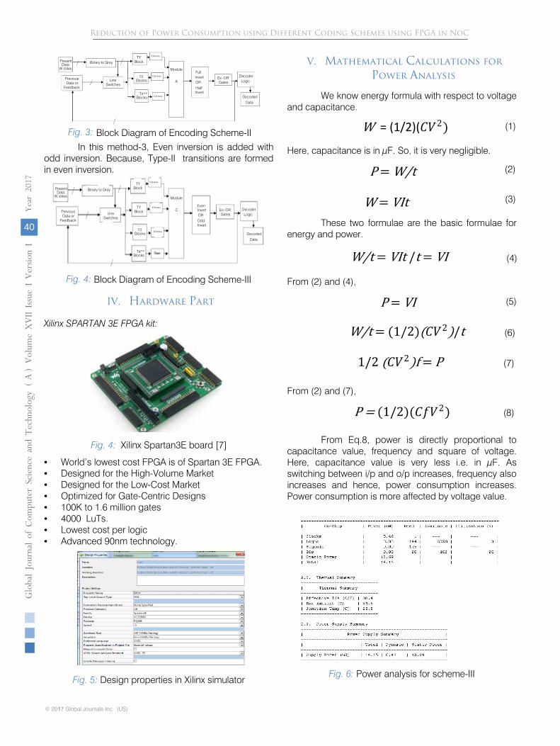
Block Diagram of Encoding Scheme-II
In this method-3, Even inversion is added with odd inversion. Because, Type-II transitions are formed in even inversion.
Block Diagram of Encoding Scheme-III
IV.
Hardware
Part
Xilinx SPARTAN 3E FPGA kit:
• World’s lowest cost FPGA is of Spartan 3E FPGA.
• Designed for the High-Volume Market
• Designed for the Low-Cost Market
• Optimized for Gate-Centric Designs
• 100K to 1.6 million gates
• 4000
LuTs.
• Lowest cost per logic
• Advanced 90nm technology.
Fig. 5:
Design properties in Xilinx simulator
From Eq.8, power is directly proportional to capacitance value, frequency and square of voltage. Here, capacitance value is very less i.e. in µF. As switching
between i/p and o/p increases, frequency also increases and hence, power consumption increases. Power consumption is more affected by voltage value.
Fig. 6: Power analysis for scheme-III
Globa
l Jo
urna
l of C
ompu
ter Sc
ienc
e an
d Te
chno
logy
V
olum
e XVII
Issu
e I Versio
n I
40
Year
2017
(
)
© 2017 Global Journals Inc. (US)1
AReduction of Power Consumption using Different Coding Schemes using FPGA in NoC
Fig. 3:
Fig. 4:
Fig. 4: Xilinx Spartan3E board [7]
Present
Data
W-bites
Binary to Grey
PreviousData or
Feedback
Line Switches
TY Block
T2
Blocks
T4**Blocks
Ones
Ones
Ones
Module
A
FullInvert OR
HalfInvert
Ex- ORGates
DecoderLogic
Decoded
Data
TY Block
T2Blocks
TY Block
T4**Blocks
Ones
Ones
Ones
Module
CEvenInvert OROddInvert
Ex- ORGates
DecoderLogic
Decoded
Data
Binary to Grey
Line Switches
PreviousData or
Feedback
Present
Data
W-bites
V. Mathematical Calculations for Power Analysis
(1)
Here, capacitance is in µF. So, it is very negligible.
(2)
(3)
(4)
From (2) and (4),
(5)
(6)
(7)
From (2) and (7),
(8)
We know energy formula with respect to voltage and capacitance.
These two formulae are the basic formulae for energy and power.
W = (1/2)(𝐶𝐶𝐶𝐶2)
P = W/t
W = VIt
W/t = VIt /t = VI
P = VI
W/t = (1/2)(𝐶𝐶𝐶𝐶2)/t
1/2 (𝐶𝐶𝐶𝐶2)f = P
P = (1/2)(𝐶𝐶𝐶𝐶𝐶𝐶2)

Table 2: Comparison different parameters of three Schemes
Parameter Scheme- 1
Scheme-2
Scheme-3
Family Spartan-3E
Spartan-3E
Spartan-3E
Device XC3S500E XC3S500E XC3S500E
Package PQ208 PQ208 PQ208
Speed 5 5 5 Clock 1 1 1
Logics 148 163 144
Signals 197 177 175
IOs 20 11 20
Dynamic Power 0.46mW
0.46mW
0.46mW
Static Power
13.69mW 13.69mW 13.69mW
• As shown in Table.2, number of logics increases
efficiency. As number of signals decreases power consumption also decreases from scheme-1to scheme-3.
• In previous system, for only one stage, i.e. Gray Encoding block, dynamic power consumption was 0.3mW.And now, in the present system after summing for all stages, dynamic power consumption is 0.46mW.From this comparison is done. We can conclude that power consumption is minimized in more amounts.
VI. Results and Discussion
a) Scheme-I In scheme-I, half invert and full invert is
performed. In full invert, 00 is converted into 11. When any one of the two is performed then inversion bit is set to 1, otherwise it is set to 0.
b) Scheme-II Simulation is done on Xilinx 14.5 ISE simulator.
It is backend design tool. In scheme-II odd inversion is
added. Type-II transitions are converted into type-IV transitions. Data coming at Network interface is from Encoder block. Then it is converted into desired encoded data which is passed through number of routers. This type of encoding is of scheme-II.
c) Scheme-III In scheme-III, there is additional inversion is
performed that is Even inversion. For that Te block is added in second stage. Here, power consumption will be less than Scheme-II because; link power consumption is minimized in more amounts.
Binary bit has some switching problem. So, they are converted into gray bits.
In scheme3, apart from Ty, T2, and T4** blocks, Te block is added which will further help in determining type of Inversion.
Detection of number of 1’s is taken placed from Ones module. Next is, majority block. It can detect major number of 1’s present in inputs to it. Data bits are passed through Module-C, checks type of inversion. Data is preceded with odd invert, even invert.
© 2017 Global Journals Inc. (US)
Globa
l Jo
urna
l of C
ompu
ter Sc
ienc
e an
d Te
chno
logy
V
olum
e XVII
Issu
e I Versio
n I
41
Year
2017
(
)A
Reduction of Power Consumption using Different Coding Schemes using FPGA in NoC
Power analysis for scheme III for gray Encoding [4]
Fig. 7:
Fig. 8: Result of Binary to gray conversion Block
Fig. 9: Result of Previous data Block
Fig. 10: Result of 2nd stage
Fig. 11: Result of Majority Block

Last output is gained by making Ex-or operations.
d) Results obtained by LCD Interfacing
To calculate report for power consumption, first, we have to interface encoder and decoder with LCD. On this LCD, we can see desired output for both stages, encoding and decoding.
Here, ‘en’ is for enable, ‘clk’ is for clock and ‘rs’ is for register select. When there is initialization of lcd rs=0. When rs=1, data is as it is written on lcd. When en=1, module is enabled or is started.
VII. Conclusion
• Encoding and decoding operation is used for security purpose. But here, main aim is to reduce power consumption in a effective way.
• Hardware part is used in such a way that cost of Spartan 3E (for Xilinx) is the lowest among different FPGA families.
• Dynamic power consumption without interfacing is calculated and compared with previous systems.
• In scheme-I, II, III, on the basis of parameters, power analysis is done.
References Références Referencias
1. Data Encoding Schemes in Networks on Chip by Maurizio Palesi, Giuseppe Ascia, Fabrizio Fazzino and Vincenzo Catania, IEEE transactions on Computer-aided design of integrated circuits and systems, vol. 30, no. 5, may 2016.
Globa
l Jo
urna
l of C
ompu
ter Sc
ienc
e an
d Te
chno
logy
V
olum
e XVII
Issu
e I Versio
n I
42
Year
2017
(
)
© 2017 Global Journals Inc. (US)1
AReduction of Power Consumption using Different Coding Schemes using FPGA in NoC
Fig. 12: Result of Last Stage
Fig. 13: Result of All connected Blocks
Fig. 14: Xilinx FPGA Spartan-3E kit withEncoded and Decoded data as o/p.
Fig. 15: Result for Scheme-1 LCD interfacing
Fig. 16: Result for Scheme-2 LCD interfacing
Fig. 17: Result for Scheme-3 LCD interfacing
2. Shivaraj MN, Ravi H Talawar, “Dynamic Power Reduction in NOC by Encoding Techniques”, IJIRST (International Journal for Innovative Research in Science & Technology) Volume 2, Issue 04, September 2015.
3. JEEVA ANUSHA, V.THRIMURTHULU, “VLSI DESIGN OF LOW ENERGY MODELING FOR NETWORK ON CHIP (NoC) APPLICATIONS”,International Journal of VLSI and Embedded Systems(IJVES), Vol 06, Article 06596; June 2015.
4. Maurizio Ascia, Fabrizio Fazzinoand Vincenzo Catania, “Data Encoding Schemes in Networks on Chip”, IEEE transaction on computer aided design of integrated circuits and systems, vol. 30, no. 5, may 2016.
5. Nima Jafarzadeh, Maurizio Palesi, Ahmed Khademzadeh and Ali Afzali-Kusha, “Data Encoding Schemes for Reducing Energy Consumption in NoC”, IEEE transaction on VLSI system, vol. 22, no. 3, march 2014.

© 2017 Global Journals Inc. (US)
Globa
l Jo
urna
l of C
ompu
ter Sc
ienc
e an
d Te
chno
logy
V
olum
e XVII
Issu
e I Versio
n I
43
Year
2017
(
)A
Reduction of Power Consumption using Different Coding Schemes using FPGA in NoC
6. Suresh Dannana, Govinda Rao Tamminaina and A.R.V. Sathish Kumar, “Data Driven Data Encoding for Low Power Application”, International Journal of Signal Processing (IJSP), Image Processing and Pattern Recognition(IPPR), Vol.8, No.10 (2015), pp.375-388.
7. Akula Soujanya, Mrs. P. Vinitha, Mr. K. Gopi, “Data Encoding Techniques for Reducing Energy Consumption in Network-on-Chip”, International Journal of Eminent Engineering Technologies(IJOEET) ,Volume 4, Issue 2 NOV 2015.
8. A.V. Manoj, S. Bhavya Sree, K. Yuva Kumar, V. Purandhar Reddy,“ Power Consumption in Network-on-Chip by Encoding Scheme”, International Journal of Innovative Research & Development (IJIRD), January, 2014 Vol 3 Issue 1.
9. D. Anisha, R. Sarathbabu, “Data Encoding Techniques for Lower Power Dissipation in NoC”, International Journal of Engineering Research & Technology( IJERT), Vol. 3 Issue 2, February – 2014.
10. Chetan. S. Behere and Somulu. Gugulothu,“ENCODING SCHEMES FOR POWER REDUCTION IN NETWORK ON CHIP LINKS”, International Journal of Research in Engineering and Applied Sciences (IJREAS), Vol. 02, Issue 02, July 2014.

This page is intentionally left blank
Globa
l Jo
urna
l of C
ompu
ter Sc
ienc
e an
d Te
chno
logy
V
olum
e XVII
Issu
e I Versio
n I
44
Year
2017
(
)
© 2017 Global Journals Inc. (US)1
AReduction of Power Consumption using Different Coding Schemes using FPGA in NoC