Embed Size (px)
Citation preview

AN ABSTRACT OF THE THESIS OF
Alex Faveluke for the degree of Master of Science in Electrical and Computer
Engineering presented on August 25, 1997. Title: Hardware Design and Protection
Issues in an AC/AC Converter;
Abstract approved:
Rene Spee
An AC/AC converter has been designed and implemented for the purpose of
providing a modular drive system with a Brush less Doubly-Fed Machine (BDFM.) This
converter is to be used in laboratory testing and also as part of a demonstration system in
the field.
All hardware needed to start and run the BDFM is now consolidated into a single
NEMA standard frame electrical equipment box. This allows easy transportation and
setup of the drive system, and will enable the BDFM drive system to be directly
compared with existing induction machine based drive systems.
Converter subsystem overviews in the body of the text and comprehensive
schematics in the appendices of this thesis describe all circuitry included in the drive
system. Sufficient construction detail is given to allow for duplication of this converter
by qualified technical personnel. While not tailored for mass production, this converter
may provide a starting point for a commercially viable design.
Redacted for Privacy

Hardware Design and Protection Issues in an AC/AC Converter
by
Alex Faveluke
A THESIS
submitted to
Oregon State University
in partial fulfillment of the requirements for the
degree of
Master of Science
Presented August 25, 1997 Commencement June 1998

Master of Science thesis of Alex Faveluke presented on August 25, 1997
APPROVED:
Major Professor, representing Electrical and Computer Engineering
Chair of Departm lectrical and Computer Engineering
Dean of Graduate Sc 146o
I understand that my thesis will become part of the permanent collection of Oregon StateUniversity libraries. My signature below authorizes release of my thesis to any readerupon request
Alex Faveluke, Author
Redacted for Privacy
Redacted for Privacy
Redacted for Privacy
Redacted for Privacy

Acknowledgements
The project and accomplishments presented in this thesis would not have been possible
without the efforts and support of several people and organizations. First, the author
would like to recognize the financial support provided by the Electric Power Research
Institute, Puget Sound Power and Light, and the Bonneville Power Administration.
Inspiration, guidance, and direction of this project was provided by Dr. Rene Spee, and
was critical to the success of this undertaking. The converter described in this thesis
would not be possible without the direct contributions and coordinated efforts of a team
of individuals, including Shibashis Bhowmik, Annabelle Van Zyl, and Brian Koch, as
well as myself Finally, I must recognize the fact that this work is an extension of a
legacy of students and faculty at Oregon State University who have put forth
extraordinary effort and commitment in researching and developing the Brushless Doubly
Fed Machine system.

TABLE OF CONTENTS
Page
1. INTRODUCTION 1
1.1 Motivation and Design Philosophy 1
1.2 Primary Intended Application 2
2. LINE AND LOAD INTERFACE 7
2.1 Input Reactor 7
2.2 Output Filter 7
2.3 Input and Output Contactors 8
2.4 Supervisory Relay 8
2.5 Bus Bleed Circuit 10
2.6 Bus Pre-Charge Circuit 10
2.7 Physical Interconnection With AC Grid Input and BDFM Load 10
3. MAIN Bus BOARD 12
3.1 Powerex/Mitsubishi Intelligent Modules 12
3.2 Two Layer Laminar Bus Structure 13
3.3 Capacitors 14
3.4 Isolated Power Supplies 14
3.5 Optocoupler Interface 15
3.6 Connections and Mounting 16
3.7 Heat Sink 16
4. INTEL 80196 MICROCONTROLLER BOARDS 17
4.1 Core Processor and Memory System 18
4.2 Microcontroller Analog Interface 18
4.3 Current Analog Interface 19
4.4 Zero Crossing Detection Circuit 19

TABLE OF CONTENTS (Continued)
Page
4.5 Output Interface to Main Bus Optocouplers 20
4.6 Fault Detection and Disable Logic 20
4.7 Serial Communication Section 21
4.8 Debugging LEDs 21
5. VOLTAGE MEASUREMENT AND PROTECTION BOARD 22
5.1 DC Bus Voltage Measurement 23
5.2 Energy Dumping Resistor Control 23
5.3 Ultimate Over-Voltage Trip Control 24
5.4 Contactor Control Interface 25
6. SYSTEM CONTROL POWER 27
6.1 Off the Shelf Line Interface Supply 27
6.2 Supply Conversion and Distribution Board 28
6.3 5V and 15V Output Buck Regulators 28
6.4 -15V Buck-Boost (Inverting) Regulator 31
7. TESTING AND RESULTS 33
7.1 BDFM Operation 33
7.2 Continuous Ratings 34
7.3 Voltage Sag Resistance Research 35
8. CONCLUSIONS AND RECOMMENDATIONS 36
8.1 Conclusions 36
8.2 Recommendations 37
8.2.1 Protection Systems 37
8.2.2 Control Algorithms 37
8.2.3 Consolidation of Hardware 38
8.2.4 Elimination of Electromechanical Contactors and Relays 38
8.2.5 Consideration of Other Topologies for BDFM Operation 39

BIBLIOGRAPHY
APPENDICES
Appendix A
Appendix B
Appendix C
Appendix D
Appendix E
Appendix F
Appendix G
TABLE OF CONTENTS (Continued)
Page
41
43
Physical Line and Load Interface 44
Optocoupler Interface 50
Isolating Power Supplies 54
61Microcontroller Boards
Voltage Measurement and Protection Board 70
Internal Power Supply Board 81
Photographs 86

LIST OF FIGURES
Figure Page
1.1 System Overview 4
2.1 Line/Load Interface 9
3.1 Main Bus Board Overview 12
4.1 80196 Microcontroller Board Overview 17
5.1 Voltage Measurement and Protection Board Overview. 22
5.2 Relay Coil Interface. 25
6.1 Converter Internal Control Supply Requirements. 27
6.2 Control Power Supply 28
6.3 Buck Regulator 29
6.4 Buck-Boost Converter 31
7.1 Input Waveforms of Drive System 33
7.2 A(I) Input and Output Currents at Full Rated Load 34
7.3a DC Bus Voltage, Diode Bridge Operating Under Voltage Sag Conditions 35
7.3b DC Bus Voltage, Active Rectifier Operating Under Voltage Sag Conditions 35

LIST OF APPENDIX FIGURES
Figure Page
A.1 Line/Load Interface 45
A.2 Supervisory Relay Scheme 49
B.1 Optocoupler Drive Interface Schematic 51
B.2a Optocoupler Drive Interface Top Side Component Placement 53
B.2b Optocoupler Drive Interface Bottom Side Component Placement 53
C.1 Isolating Power Supplies Schematic 55
C.2a Isolating Power Supplies Top Side Component Placement 57
C.2b Isolating Power Supplies Bottom Side Component Placement 57
D.la Microcontroller Core System Schematic 62
D. 1 b Microcontroller Power and Interface Schematic 64
D.1 c Microcontroller Current and Zero Crossing Schematic 66
D.2a Microcontroller Board Top Side Component Placement 68
D.2b Microcontroller Board Bottom Side Component Placement 69
E. 1 a Voltage Measurement Schematic 71
E.lb Relay Control Interface Schematic 73
E.1 c Ultimate Overvoltage Protection Schematic 74
E.2a Voltage Measurement and Protection Board Top Side Component Placement 79
E.2b Voltage Measurement and Protection Board Bottom Side
Component Placement 80
F.1 Internal Power Supply Schematic 82
F.2 Internal Power Supply Top Side Component Placement 85
G.1 a Optocoupler Interface, Top Side of PC Board 87
G.1 b Optocoupler Interface, Bottom Side of PC Board 87
G.2 Main Bus Board Assembly 88
G.3 Completed Converter, Rack Mounted and Ready for Use 89

LIST OF APPENDIX TABLES
PageTable
A.1 Line/Load Interface Power Component Description 46
A.2 Line/Load Interface Power Component Wiring 47
B.1 Optocoupler Interface Component List 52
C.1 Isolating Power Supplies Component List 56
D.1 Microcontroller Core System Component List 63
D.2 Microcontroller Power and Analog Interface Component List 65
D.3 Current Sensing and Zero Cross Detection Component List 67
E.1 Voltage Measurement and Protection Component List 72
E.2 Relay Control Interface Component List 75
E.3 Ultimate Overvoltage Protection Component List 76
F.1 Internal Power Supply Component List 83

Dedication
This thesis is dedicated to Erin Giltner, for her unwavering support, encouragement, and
help in every aspect of my life.

Hardware Design and Protection Issues in an AC/AC Converter.
1. Introduction
1.1 Motivation and Design Philosophy
The Brush less Doubly-Fed Machine (BDFM) has been developed at Oregon State
University. Research and development efforts for this machine focused on design and
implementation issues to be resolved as a step in commercialization of this technology.
This thesis describes a specialized bi-directional power converter designed and built at
the University to test and demonstrate a BDFM prototype drive system.
The converter was built as part of a BDFM drive system intended for real world
testing and application. Much thought and design effort was put into making this system
both applicable and survivable in an industrial setting. There are plans for application as a
long term demonstration system in an appropriate location.
While the converter, as built, is not suitable for mass production, it is intended to
show the possibility of commercial manufacture given some additional design effort from
a company experienced in bringing prototype converters to the production stage. Full
hardware design detail of the implemented converter is given in this thesis, with
schematics, layouts, and bills of material provided in the appendices.
The converter is built on a 17 inch square aluminum panel for fitting into a
NEMA (National Electrical Manufacturer's Association) standard frame electrical
equipment box. This gives a proof-of-concept prototype that is suitable not only for
research work in a university development laboratory, but also for realistic testing in a
real world industrial environment. The converter is rated 3kVA on the input, and 6kVA
on the output, suitable for application with a BDFM designed to deliver 15 horsepower to
a mechanical load.

2
1.2 Primary Intended Application
The converter was built as a component of on-going research studying design and
application issues of the Brushless Doubly Fed Machine (BDFM.) The BDFM provides
an adjustable speed drive with lower power rated semiconductors by using separate
power and control windings. The power winding may be connected to a 60Hz, 341
voltage source supply, while the control winding is excited with a regulated set of 34)
currents from an adjustable frequency converter. If the BDFM is operating in the
synchronous mode of operation, the speed can be controlled with a low power
requirement from this converter. In this synchronized operating region of the BDFM,
rotor speed is locked to a speed determined by the two input current frequencies, and the
magnetic pole numbers of the respective windings. This speed is given by [1]:
Nr fc x 60(rpm)Pp + Pc 1.1
where Nr is the shaft speed in r/min, fi), and fc are the frequencies applied to the
power and control windings, respectively, and Pp, and Pc are the pole numbers of the
power and control windings.
To study and develop physical prototypes of these machines, a test bed has been
constructed [1]. This test bed includes electrical instrumentation for both the power and
control winding inputs, mechanical torque and speed transducers, and a computer to log
test data. A DC drive is provided as an adjustable torque and speed load. As the BDFM
can also function as a generator, this DC drive may also be run as a motor, which
provides a prime mover for a generation system under test.
The BDFM requires a converter with bi-directional power flow capability to take
full advantage of its variable speed range. Also, an ideal drive system would seamlessly
provide synchronization of the machine on start up. The typical method of synchronizing
the BDFM is to allow it to run up as an induction machine, with only one winding

3
excited, and then to apply control excitation as the machine accelerates through the
desired speed.
While good success in testing and development of the machine has been attained
using a large thyristor based resonant converter, it was desired to show the commercial
applicability and viability of the BDFM drive system. A modular drive system has been
implemented. This system integrates an adjustable frequency bi-directional converter
with all electrical control gear needed to time and energize the control winding as needed
for synchronization and control.
The converter has been built into a standard NEMA frame electrical box. All
control logic and switch gear needed to synchronize and control the BDFM has been
included. This yields a modular system, which can be applied as simply as other forms of
adjustable speed drives. It also allows for direct comparison to be made with existing
technologies in real world environments. This converter was built to help bring the
BDFM from the lab to the shop floor, at least on a demonstration basis. Fig. 1.1 gives an
overview diagram, showing connection of the main component parts of the converter, and
illustrating how the BDFM windings are connected to control hardware. The systems
shown will be discussed in detail in later chapters.
Bi-directional power flow requires control over the rectifier devices. This adds
some cost to the system, because the ordinary input rectifier diodes are now replaced with
an active transistor (IGBT) bridge and associated control hardware. However, the initial
investment in a slightly higher cost converter topology delivers significant benefits that
can make the bi-directional converter a better and more economic solution in the long
run.
First, in a current controlled active rectifier such as the one described in this
thesis, input currents are regulated to be sinusoidal. This effectively eliminates power
quality problems caused by harmonic current draw, and allows the drive to meet
emerging international standards such as IEEE 519 and IEC 555 [2].

INPUT D LINE D230U,30
SYSTEM CONTROL POWER
LINE/LOAD INTERFACE
<LINE AND POWER WDG SECTION>
JI i 80196
OUTER LOOP
CONTROL
OUTPUT TO BDFM POWER WINDING
BDFM
MAIN BUS BOARD
RECT. INV.
IGBT FAULT FEEDBACK
RECT. IGBT INU GBT CONTROL CONTROL
i80196 i80196
RECTIFIER I NUERTER
CONTROL CONTROL
OUTPUT TO
BDFM CONTROL WINDING
LINE/LOAD INTERFACE
<CONTROL WINDING SECTION>
1
VOLTAGE MEASUREMENT
AND PROTECTION
BOARD
4=.

5
The rectifier's control algorithm allows control over input displacement power
factor. In this way, the energy storage of the DC bus can be used to allow the converter
to act as a capacitive load on the grid, providing compensation for electric machinery
operating at lagging power factor. The BDFM main winding typically draws lagging
power factor, and the option of using the converter to provide capacitive compensation to
improve power factor and reduce total kVA requirements on the grid has been
demonstrated in [11]. In many factory settings it may be advantageous to use the active
controlled rectifier to correct for other poor power factor loads [2].
The active rectifier input stage acts as a voltage boosting converter, enabling the
drive to "ride-through" voltage sags. Voltage sags are a fairly common occurrence and
traditional diode based rectifier adjustable speed drives can be very sensitive to these. If
accurate, stable speed control is needed, even short duration sags can cause drive
shutdowns. In addition to providing a BDFM specific modular adjustable speed drive,
the converter has been used as a test bed for development of sag resistant rectifier control
algorithms [3]. The rectifier is used to compensate for input voltage reduction by
increasing the boost ratio, which maintains the DC bus reasonably constant. Because the
DC bus voltage is maintained constant, the inverter retains full control over output
current, and suffers no loss of output current accuracy or range.
The converter has been designed with experimentation in mind, both in terms of
control algorithms and BDFM design. It contains several protection features to enhance
survivability. These are also suitable for the industrial environment, where accidental
shorts, overloads, and misconnections can affect the life of installed electrical equipment.
The considerable expense of factory down time and repair can easily justify the initial
expense of providing comprehensive protection.
This thesis has been written as documentation on an implemented bi-directional
converter. It concentrates on the physical electronics, leaving the software and control
algorithms to other writers, [2] and [11]. The author hopes that this document may be
useful in applying this converter in the field, and in the design of similar hardware for
commercial application. Thus, all construction details are thoroughly described with

6
explanatory overviews given in the body of the text and comprehensive appendices
giving full schematics and bill of materials lists for construction.

7
2. Line and Load Interface
The converter requires an interface to both the line and the connected machine.
This interface contains hardware used to connect the converter to the input grid and the
driven machine, as well as an additional contactor for switching in the BDFM power
winding, which is excited directly from the 60Hz grid voltage. A schematic is provided
of the Line and Load Interface in Figure 2.1.
2.1 Input Reactor
A three phase, 7.5mH line reactor [4] is provided in the enclosure. This reactor is
needed for active rectifier control. While many commercial drive systems require an
external line reactor, this part was included to provide a more modular system, in which a
user does not have to select or provide connection to any external parts. The reactor is
thermally limited to 8 amps continuous, but for short periods can be loaded up to 12 amps
with no noticeable loss in inductance. Inductor requirements and selection issues are
discussed in detail in the appendices of [5].
2.2 Output Filter
Some output filtering was needed due to electromagnetic interference (EMI)
caused by fast switching rise times driving transient current into cable capacitance. Three
small inductors wound on standard iron powder type toroids and placed in series with the
converter output provided enough filtering to eliminate noise problems with the RS232
communication links. A full description of these inductors is given in the power
component wiring list given in Appendix A.
8
2.3 Input and Output Contactors
For ease of test and development, the converter is connected to the input grid and
the load by power contactors, designated X2 and X3 in Fig. 2.1. These allow complete
isolation in the case of overload conditions. In addition, a contactor is provided to switch
in the BDFM main winding, which simply requires 60Hz three phase power. All
contactors and relays are driven from the "Contactor Control Interface" on the Voltage
Measurement and Protection Board, as discussed in Chapter 5.
2.4 Supervisory Relay
Enabling and disabling control over all power interfacing relays is provided by a
classic industrial control latching circuit. A small three pole relay (designated as X4) is
used in conjunction with two push buttons, one being normally open, for "enable" and the
other being normally closed, for "disable." This relay is set up to latch in when the
"enable" button is pushed, by providing coil energization from one of its own normally
open contacts. The "disable" switch is in series with the coil, and when it is pushed, the
coil circuit is de-energized, which drops out the relay. If the power supply fails, such as
would happen in the case of a momentary grid outage or blackout, the supervisory relay
drops out and can only be latched back in when the user pushes the enable button.
The supervisory relay provides the only source of positive voltage to all other
relay and contactor coils in the system. In this way, no logic error or glitch can remove
the ability to disconnect the system from the grid, and the system cannot be inadvertently
started until the "enable" button has been pressed. A schematic of the supervisory relay
control circuit is given in Appendix A.
TBI -INIMUM TBI -I N2MEN. TM-1N3
1111111111
GROUND >TBIC4
LINE 230VA0
X1 IN1
IN2
IN3
0 0 0 0 0 o
OUT1
OUT2
OUT3
CN1 A
CN1 B
CN1 C
B_PIAR
POWER WNDG OUTPUTS
30LINE REACTOR
G
DUMP RESISTORS
LINE FUSES R7 1R8 R61 R5 FRAME GND
X2 RECTIFIER INVERTER X3 IN1 OUT1 ti DC +
I N 1 0 OUT1 CNI -0
IN2
I N3 0 0 0
0 OUT2 OUT3
e, ti
BK
DC
BK ti
ti
IN2
IN3 0 0
OUT2 cm E
OUT31-01../ I CM -F B_CNTRL
CNTRL WNDG OUTPUTS
X5 BLEED RESISTOR
P1 X5-1
X5-1NO X4-3"g P4
X4-3NC P2 X5-2
0X5-2NO R3 X5 -3
X5 -3N0 PRE-CHARGE RESISTORS
NO

10
2.5 Bus Bleed Circuit
In addition to the enabling function, the supervisory relay acts to drain the charge
from the DC bus on system shutdown. When the system is disabled for any reason, a
normally closed contact of the relay connects a 50 ohm resistor across the DC bus,
draining practically all charge off the large storage capacitance in less than one second. If
power is externally disconnected, the supervisory relay will drop out, giving the same
result. This feature has made working on and debugging the converter much easier and
safer because it was not necessary to manually discharge the bus capacitance, or to wait a
long period of time for a high value bus bleed resistor to drain the charge to a safe level.
2.6 Bus Pre-Charge Circuit
On system start-up, a small relay designated X5 is used to automatically pre-
charge the bus through three 50 ohm power resistors. When the input contactor is
commanded to close, this pre-charge relay initially connects the grid through these three
resistors. This prevents destructive inrush surge on start up. After a delay of
approximately one second, the main input contactor is closed. This delay is generated by
a simple one shot type circuit implemented in the Contactor Control Interface section of
the Voltage Measurement and Protection Board, which is described in Chapter 5.
2.7 Physical Interconnection With AC Grid Input and BDFM Load
This converter is part of an integrated package intended to demonstrate and test
the Brushless Doubly-Fed Machine in an industrial environment. A well qualified field
technician will be able to successfully install and operate the system. With these goals in

11
mind, interconnection hardware was chosen to facilitate field installation by individuals
experienced in installing other types of drive equipment.
An input terminal block is provided for the 230V grid and ground connection. A
heavy-duty 7 pin connector is supplied for a cable from the machine. This provides
convenient and error-free interface to both the power winding and the control winding of
the BDFM as well as a secure ground connection from the converter box to the machine
frame.

12
3. Main Bus Board
Capacitors, interconnections, isolated power supplies, interface optocouplers and
all power electronics for both the active rectifier and the inverter are included on the main
bus board. This yields a modular system which is easy to build, test, and mount into the
final system. An overview of the Main Bus Board is shown in Fig. 3.1.
RECTIFIER DC BUS POSITIVE
11!I INVERTER fr:& U DC ÷ DC +
Eav 3 BULK ENERGY V :1
IANk 3 BRAKE STORAGE
(4X62OurT BRAKE 41M1
DC 0 0 DC
POWER MODULE DC BUS NEGATIVE
POWER MODULE
1 1 1 1 1 1 1 I I I I I I I I I I I I ISOLATED ISOLATED 1 1 1 1 1 1 1 1 1 1 1 1 1 1 1 1 1 1 1 SUPPLY SUPPLY
INTERFACE GENERATOR GENERATOR INTERFACE SECTION OUT: OUT: SECTION
4 X 15U 4 X 15U OUT: 15V MODULE ISOLATED ISOLATED OUT: 15U MODULE CONTROL LEVEL SUPPLIES SUPPLIES CONTROL LEVEL
IN:24V IN. 24V IN. pC 5U LOGIC IN: pC 5V LOGIC
24V5V LOGIC DRIVERS 24U 5U LOGIC DRIVERS DUMP
pC i 80196 CONTROL pC i80196FAULT FAULT(ON UM&PDETECT RECTIFIER INVERTER DETECTBOARD)CONTROL BOARD CONTROL BOARD
Figure 3.1 Main Bus Board Overview
3.1 Powerex/Mitsubishi Intelligent Modules
All power electronics on the main bus board are included in two
Powerex/Mitsubishi PM3ORSF060 IGBT based Intelligent Power Modules [6]. These
consist of 6 bridge IGBTs and associated freewheeling diodes, and a 7th IGBT to

13
implement a braking or energy dumping scheme. The bridge IGBTs are rated for 30 A
maximum continuous collector current and the auxiliary brake IGBT is rated for 10 A
continuous collector current. These modules take logic level signals and switch internal
IGBTs to provide power switching waveforms. Also, over-current protection and
diagnostic "fault" signals are provided to enhance survivability of these modules in the
event of overloads or inadvertent short circuits.
3.2 Two Layer Laminar Bus Structure
In switching converters, inductance between bulk energy storage capacitors and
the switching bridge leads to di/dt induced voltage spikes, which can destroy the
switching transistors. One of the primary goals of the main bus board design was to
minimize these undesired parasitic inductances. To this end, a double sided printed
circuit board was designed to implement a laminar bus structure. This structure
minimizes enclosed current loop areas. Wide planes of copper on the top side of the
board are dedicated for the positive rail of the bus, and likewise, the bottom side is
primarily used as the negative. Because these planes are positioned directly across the
board from each other, the current loop area is minimized. A photograph of the main bus
assembly is provided in Appendix G.
Thermal effects of trace heating were carefully considered. Trace heating is
related to the current density in a trace, and design charts are provided by board material
manufacturers. To answer concerns regarding plated thru-hole current carrying
capability, DC test currents of up to 20 A were driven in selected power connection thru-
holes. Even though the tests showed no excessive heating, care was taken in the
assembly to ensure correctly made solder joints, in which a connecting "fillet" is formed
on both sides of the printed circuit board.
The printed circuit board construction method used for the DC bus assembly is
economical and easy to manufacture. In converter designs for current levels much in
excess of 20 A, the use of a fabricated laminar bus structure should be considered. In a
fabricated laminar bus structure, sheets of copper are cut to size and separated with

14
insulating material. High currents can be dealt with efficiently by simply increasing the
thickness of the copper sheet.
3.3 Capacitors
The capacitors used on the main bus board serve two purposes. One is to provide
bulk energy storage, enhancing stability and enabling constant power delivery from a
varying source. The other is to provide a source of charge from which high frequency
currents may be drawn, ideally without creating large transient voltage spikes.
To accomplish these two functions, we use four electrolytic caps, of 6201,1F each,
and two film type caps, of 0.474F each. The electrolytics store bulk energy, while the
film capacitors have the low self inductance needed to limit voltage transient generation
with the fast current rise times seen when switching the IGBTs. These film capacitors are
mounted as close as reasonably possible to the module positive and negative input pins.
In a commercial converter, the amount of capacitance would probably be reduced to a
minimum dependant on capacitor ripple current rating. With the implemented converter,
a very large bus capacitance (2480g) was designed in to enhance stability with
developmental software and hardware.
3.4 Isolated Power Supplies
Each of the two Powerex/Mitsubishi Intelligent Modules used requires four
isolated power supplies. These provide gate drive power to the IGBTs and power for the
control and protection logic of the module. One supply referenced to the negative power
rail handles all three of the "lower" bridge IGBTs and the "brake" IGBT. Three separate
supplies must be used for the "upper" devices, because their emitters are not connected
and, in fact, when switching are separated by a fast rise time square wave at the system
bus amplitude. This presents a challenge because current pulses will be capacitively
coupled in any common mode capacitance between these supplies, leading to supply

15
noise and dielectric problems. Obviously, any common mode capacitance should be
minimized.
In the converter, the isolated power supplies are generated from two independent
flyback converters, one each for the rectifier and inverter. Fairly thick build-ups of inter-
winding tape are used in the flyback coupled-inductors to provide good dielectric
isolation and to minimize inter-winding capacitance. The direct outputs are set to
between 18 and 20V, from which linear regulators are used to derive 15V, giving a high
degree of output voltage accuracy and noise immunity. In each supply, a current-mode
control chip, the UC3845 handles all the control functions [7] and drives an N channel
MOSFET to charge and switch the primary winding. A full schematic and detailed
design description of these flyback converters can be found in Appendix C.
3.5 Optocoupler Interface
Optocouplers are used to interface and level shift ground referenced logic to the
module input pins that are referenced to the emitters of the IGBTs. The optocouplers
interfacing to the "high side" IGBTs must be able to withstand severe common mode
transients with dv/dt on the order of 8000V/tis. The optocouplers selected have common
mode rejection ability up to 15kV/gs, under voltage magnitude swings of 1500V. [7] For
even higher common mode rejection capability, fiber optic links have been used,
however, due to advances in optocoupler technology, fiber optic links are no longer
needed for drives functioning off the 230 or 460 volt line. A full schematic of the
optocoupler interface circuit can be found in Appendix B.
The layout of the optocoupler interface section must be carefully designed.
Maintaining traces associated with each "upper" IGBT far apart minimizes capacitive
coupling, and reduces the risk of a flash-over on the board. The final layout design
conforms to standards given in [8] for trace separation in power converters. Photographs
showing the circuit layout are provided in Appendix G.

16
3.6 Connections and Mounting
Standard 0.250 inch male tab connections are provided for all power wiring to be
connected to the main bus board. Small 0.100 inch center "Molex" type headers are
provided for all control and logic level feedback signals. Tubular spacers and screws
mount the board to the heat sink, and extra support is provided by stand-offs to the main
panel.
3.7 Heat Sink
A heat sink is needed to dissipate the IGBT switching and conduction losses. An
off the shelf aluminum extrusion was selected and modified to mount in the enclosure.
Two small fans force air through the heat sink fins and out the ventilation screen in the
case. This forced air stream is also directed through and around the input reactor, which
would otherwise to run hot at its full rated current in the enclosure used. Detailed
information on heat sink requirements and selection is given in [9].

17
4. Intel 80196 Microcontroller Boards
All current control, switching pattern generation, and outer loop control functions
are implemented on three identical printed circuit boards using the Intel 80C196KC
microcontroller. An overview of these boards is shown in Fig. 4.1. These boards were
designed and built especially for the converter and incorporate a number of features
helpful for power electronics control work.
300Nimiosok Qoc_IN I (FROM UM &P DEBUG LEDS
I 4CIEM BOARD)
co
cn
I a 'II
111.=
ANALOG FILTERS
ND VOALTAGE CLAMPS
PORT 1
i80C196KC A TO D INPUTS
ADD/ DATA PINS
/PO
16 BIT FLASH ROM MEMORY BUS
(32K WORDS) ALE
CURRENT SENSOR 5V
REF UART INTERFACE x x HSO HSI. 0
ZERO CROSS DETECTION
SERI AL (ON RECTIFIERINTERFACE CONTROL ONLY)FAULT OUTPUT OM UE
51) MONITOR BUFFERLOGIC i8051 C ENABLE OUTPUTS
+-10V e' ,t+
RS232 +5U UCC FAULTS
L.) (..)T NI GBT GATE COMMANDS
I TX_OUT) 141
I-- (FROM 60HZ( TO MAIN BUS BOARD)1 ZERO CROSSGND
(FAULT MONITOR TRANSFORMER) TO SLAVED BOARD)
RECT NV
Figure 4.1 80196 Microcontroller Board Overview
Control software for the current controlled rectifier and inverter was written in
80196 C and assembly code, and is described in detail in [10]. Control software driving

18
outer loop supervisory control and user interface functions is described in detail in [11].
It is important to note that the rectifier, the inverter, and the outer loop control boards are
completely separate entities. The inverter control generates commands to regulate
current into the connected load, the rectifier regulates the input currents and the DC bus
voltage, and the outer loop control provides timing and supervisory functions for user
interface and automatic control over the machine. The outer loop control board sends
commands to the inverter and rectifier control boards with an RS232 serial data link.
This is described in [11].
4.1 Core Processor and Memory System
The converter's microcontroller boards incorporate the Intel 80196KC, running at
16MHz. Two Flash programmable ROMs provide program memory, organized as 16 bit
words for maximum bus transfer speed [12]. Simple interface logic to demultiplex the
combined address/data bus is implemented with two 74ACT373 eight input latch ICs. A
dual row pin header provides access to most of the bus control and data pins, facilitating
system debugging and bus interface construction. Schematic diagrams in Appendix D
shows the Core Processor and Memory Interface in detail.
4.2 Microcontroller Analog Interface
The Intel 80196 family incorporates an analog to digital converter and an 8 way
multiplexer, for measurement of 8 independent voltage inputs. On the 80196 board, a 9
pin Molex style connector is provided for connection to these. Each port pin is protected
by a series resistor and Schottky diode clamps to power and ground. Noise filtering is
provided by a small capacitor in parallel with each input, which also serves to provide the
small amount of charge needed for the internal sampling circuit. The 80196 provides a
separate analog voltage reference which is supplied by a 5V reference IC powered from
the board's 12V analog rail [13]. The rectifier control board monitors the system bus

19
voltage on analog-to-digital A-D#4, after conditioning by circuitry described in 5.1. The
schematic diagrams of Appendix D show the Microcontroller Analog Interface in detail.
4.3 Current Analog Interface
Two Hall effect current sensors are mounted directly on the rectifier and the
inverter 80196 boards [14]. On the rectifier control board, the sensors monitor the AO
and BO input currents. On the inverter control board, the sensors monitor the A4 and BO
output currents. The outputs of these are level shifted, amplified, and buffered with an
operational amplifier circuit. These buffered voltages are then fed into two of the analog
to digital input ports on the board, A-D#1 and A-D#2. They can be easily disconnected if
it is desired to use A-D#1 and A-D#2 for general purpose analog voltage inputs. A
schematic of the Current Analog Interface is shown in Appendix D.
4.4 Zero Crossing Detection Circuit
The rectifier controller must have "zero crossing" information derived from the
input line voltage. This enables synchronization to the 60Hz grid with variable phase lag
for power factor control. The microcontroller receives this signal on one of its HSI (high
speed input) port pins, which requires a reasonably clean square wave at the line
frequency for proper operation. A zero cross detection circuit is implemented on the
rectifier 80196 control board. While the bare printed circuit boards are identical, the
inverter does not need zero crossing information, and this circuit is not built up on the
inverter control board.
A comparator circuit is implemented to interface with a sine wave input. The
input is ground referenced on the board, attenuated, and filtered by an R-C network.
Divider resistors provide DC attenuation by a factor of 2, and the addition of a single
capacitor provides a single pole filter with corner frequency of about 3.2kHz. The output
of this simple filter is then compared to ground. Added hysteresis helps prevent
oscillation close to the zero crossing point by introducing separation between the negative

20
switching threshold and the positive switching threshold. These are set at 0.000V for the
positive, and 0.005V for the negative threshold. A schematic of the zero cross detection
circuit is shown in Appendix D.
A small 230V to 7.6VAC transformer is used for isolation purposes, virtually
eliminating any common mode noise problems. This transformer is external to the 80196
board and connects to a small two pin header provided for this purpose.
During testing, the Zero Crossing Detection circuit occasionally generated short
glitches (multiple transitions) on the HSI.0 line. The rectifier control software was
modified to reject these multiple transitions. These occasional glitches could be
eliminated by either a lower cutoff frequency zero crossing detect filter, a higher level of
hysteresis, or a combination of both.
4.5 Output Interface to Main Bus Optocouplers
Both the rectifier and the inverter control boards connect directly to the main bus
optocoupler inputs. Positive asserted, relatively high current (approximately 15mA)
signals turn on the optocoupler LEDs commanding the respective IGBTs to switch on.
These outputs are buffered with a special tri-state bus driver chip capable of providing
sufficient drive current to the optocoupler inputs. Positive assert drive was selected to
ensure that if for any reason power is disconnected from one of the controller boards, the
optocouplers will not be turned on when outputs are pulled to ground by the on-board
driver's internal protection diodes.
4.6 Fault Detection and Disable Logic
An auxiliary flash-programmable 8051 family microcontroller located on the
rectifier control 80196 board monitors all eight fault detection optocoupler outputs from
both the inverter and the rectifier. If a "fault" situation persists for more than 1 ms, the
chip disables the inverter and rectifier output buffers, effectively commanding all IGBTs
to turn off. The Powerex/Mitsubishi Intelligent Modules provide protection against short

21
duration overloads, but are not intended to be cycled indefinitely in a faulted condition.
The monitoring software was written in 8051 assembly language; this code is listed in
Appendix D.
A "slaving" connector is provided on both the rectifier and inverter control
boards. When these connectors are jumpered together, the auxiliary 8051 fault monitor
circuit on one of the 80196 boards controls the output drive buffer on both the rectifier
and the inverter boards. All eight fault signals from the rectifier and inverter are fed to
this fault monitor circuit, which disables both the rectifier and the inverter in the event of
a long duration overload.
4.7 Serial Communication Section
The 80196 microcontroller provides an internal UART with serial transmit and
receive capability. A single chip, the MAX232 [15], generates needed voltages and level
shifting to provide an RS232 level interface. This RS232 interface is used for board-to
board communication within the converter, and may also be used to connect to an
external terminal for debugging and development purposes.
4.8 Debugging LEDs
To assist in debugging the system, an 8 LED bar graph is provided on port 1 of
the 80196. This has been found extremely useful, especially on the rectifier board, where
the bar graph is used to display system status and results of software fault protection. A
connector is provided as well, on which an oscilloscope probe may be attached to
monitor converter state on a real time basis.

22
5. Voltage Measurement and Protection Board
Bus voltage measurement, overvoltage protection, and contactor coil interface is
provided by the Voltage Measurement and Protection Board. An overview of this board
is presented in Fig 5.1.
TRIP LEUEL OURI DC BUS +> VOLTAGE ENERGY DUMPINGLTPVDC <NU_BRKSENSINGMEASUREMENT RESISTOR CONTROLANALOG
TRIP LEVEL OUR UTPIOC BUS -> SETTING AND 8851 DIGITAL CONTROL OEC_BRK I
ATTENUATION AND COMPARISON AND TIMING
DIFFERENTIAL TO GROUND REF'D ANALOG LEVEL 000 0011/17(
!PIP POINT T1711101NT
--<VOC OUT
CONTACTOR --<X1 COIL OVERUOLTAGEjULTIMATE CONTROL INTERFACE
TRIP <X2_COIL
SENSING, LATCH DRIVE INPUTS: 5V AND ISOLATED kl_CNTRO) POSITIVE ASSERT LOGIC OUTPUT
OUTPUT: OPEN COLLECTOR 1X2_CNTRI> PULL DOWN TRANSISTORS
FOR 24VDC COIL DRIVE <7.777.1 1X3_CNTRI)
DISABLE INPUTS: 5V LOW ASSERT LOGIC (SWITCH <X5_COIL
1X4_CNTRL TO GNO TO DISABLE)
Figure 5.1 Voltage Measurement and Protection Board Overview

23
5.1 DC Bus Voltage Measurement
At the heart of the Voltage Measurement and Protection board is a differential
voltage measurement scheme that rejects the common mode swings of the DC bus.
Because the bus is derived from a rectified line source, the absolute DC value cannot be
measured with respect to ground.
The differential scheme uses two precision high voltage divider networks,
bringing the voltage down to a level compatible with low voltage analog circuitry [16]. A
differential amplifier circuit then measures the difference between these two signals, and
buffers the output. The final attenuation ratio is designed to give 1V out for every 100V
on the DC bus, which will allow up to 500V to be measured with a 5V analog to digital
converter. This output is then used for the control of energy dumping resistors and is also
provided as an output for connection to the rectifier's microcontroller board. The rectifier
controller uses this signal to monitor the DC bus voltage and attempts to hold the bus
voltage to a set level. This circuit has been carefully tested and gives accurate and
reliable output.
5.2 Energy Dumping Resistor Control
Because the rectifier control software routines cannot be fast enough to
compensate for all conceivable transients or regeneration conditions, an analog control
scheme is needed to remove energy from the DC bus in the event of a system over-
voltage. This is accomplished with the use of "dump resistors," or power resistors
specifically intended to quickly remove energy by direct connection to the system DC
bus. Four 100W, 100 ohm wire-wound power resistors have been used for the energy
dissipation element. Power switching control is provided by the "brake" IGBTs
provided in the power modules. Two resistors are paralleled and attached between the

24
positive DC rail and the collector of each brake IGBT. At a bus voltage of 400V this
means each brake IGBT will conduct 8 amps and each of the four resistors will dissipate
about 1.6kW. Because the resistors have limited heat dissipation ability, this condition
must not persist indefinitely.
Control of the "dump" resistors is provided by two comparators and an 8051
family microcontroller. On board potentiometers allow the user to set two analog
voltages as "trip points." This effectively gives a hysteresis band which starts the
energy dumping action at an "upper trip point" and continues this until a "lower trip
point" has been reached. This prevents oscillation of the dump circuit under normal
conditions. The microcontroller provides a timing function to roughly monitor resistor
dissipation. A counter of "dissipation time" allows up to two seconds of dump operation
in any 40 second period. This counter continuously subtracts an amount representative of
the resistor's steady state dissipation ability and adds an amount representative of the
actual dissipation if and only if the dump circuit is firing. If this two seconds of
dissipation allowance is exceeded, the system contactors are tripped out, isolating the
converter from the grid and the load. A full schematic of the dump control circuit and the
program code monitoring the resistor dissipation are both shown in Appendix E.
5.3 Ultimate Over-Voltage Trip Control
If the primary DC bus voltage control Tails for any reason, a back up circuit has
been provided to shut down the system in the event of a severe over-voltage. This circuit
was designed with simplicity in mind, and consists of only a few resistors, a series
combination of Zener diodes, and an SCR. If the voltage is high enough to cause
sufficient current in the Zener network, the SCR fires, turning on an optocoupler input
diode. The output of the optocoupler is connected to the "disable" input of the contactor
control circuitry, which opens all contactors to isolate the converter from the grid and
load. The disable signal is asserted until the system is power cycled. A schematic of the
Ultimate Over-Voltage Trip Control circuit is shown in Appendix E.

25
5.4 Contactor Control Interface
A method of interfacing low power logic to the input and output contactors must
be used. This is achieved in the Contactor Control Interface section of the VM&P board,
using comparators for input detection and discrete transistors for output to the contactor
coils. All the coils are operated at 24VDC, which is convenient for electronic control.
The interface section uses LM339 quad comparators for logic level input sensing
[16]. The input voltage is compared to a reference generated from the on-board power
supply. As shown in Fig. 5.2, the inputs are deliberately loaded with 271cf2 to ground, in
order to ensure an off condition if a connector is unplugged. A 10kS2 series resistor helps
protect the comparator input from transients, and provides hysteresis in combination with
a 1001d2 positive feedback resistor. A full schematic of the relay interface circuitry is
shown in Appendix E.
RELAY + CONTROL
+12V VOLTAGE -I-
Jx. 2 1. Bk
1N4002
100k
Jx.1 10k
I Xx_I N
Jx. 2 27k DIVIDER
1.2k 2N2222A
REF I GND >-- (3.24W
Fig 5.2 Relay Coil Interface
To close a relay or contactor, the board connects a source of positive power from
the supervisory relay to each actuating coil and switches the other coil pin of the target
relay or contractor to ground. All contactors and relays are switched with small NPN
transistors, with the exception of Xl, which due to a higher coil current (300mA) is
switched by an N channel MOSFET. Freewheeling diodes across the outputs allow
inductive current in the relay coils to ramp down without generating voltage transients.

26
Full schematics of the logic interface is given in Appendix E, and the supervisory relay
scheme is pictured in Appendix A.

27
6. System Control Power
The converter uses several different power supply voltages for logic, analog
circuitry and auxiliary functions. The supplies required are summarized in Figure 6.1.
Voltage
+24 V
+15 V -15 V +5 V
Function Current Rating 4.5 AContactors and Relays, Heat Sink Cooling Fans, Isolated
Supply Generator Inputs Analog Positive Supply 0.5 A Analog Negative Supply 0.35 A Digital Logic Supply 5.0 A
Figure 6.1 Converter Internal Control Supply Requirements.
6.1 Off the Shelf Line Interface Supply
The converter's power supply system is a combination of a commercial off the
shelf supply and custom hardware. The off the shelf supply is an open frame, universal
input (90 to 260 VAC line) switcher capable of delivering a regulated voltage of 24VDC
at up to 4.5 A. This provides a safe and cost effective interface to the grid, and the
capability to ride through input voltage sags down to less than 50% of nominal. Sag ride-
through is one of the features of the converter, and providing stable power for logic and
control is one critical factor in attaining this. [3].

28
AO ED-
BO ED-
INPUT LINE
230W\1,30
4- /
GRID INTERFACE SUPPLY
PHI HONG UNI UERSAL INDUSTRIAL 11014
90-260VAC IN 24VDC OUT
7] 24U
-1°
LOGIC SUPPLY BUCK REGULATOR
INPUT: 24V
OUTPUT:+5U, 5A
ANALOG POSI TI VE BUCK REGULATOR
INPUT: 24V
OUTPUT: +15U, 1A
ANALOG NEGATIVE INVERTING REGULATOR
+15V
INPUT: 24V OUTPUT:-15U, 400mA
<71D
Figure 6.2 Control Power Supply
6.2 Supply Conversion and Distribution Board
The off the shelf switching supply feeds a separate Supply Conversion and
Distribution Board, which uses three switching regulators to provide the needed +5, +15
and -15V. The switching regulators derive these supplies with reasonable efficiency, and
the thermal dissipation is taken care of with small, inexpensive PC board mounted heat
sinks. Standard 5 pin connectors are provided on the board, carrying all four supplies and
a ground for harnessing to other system components. The functionality and design of the
distribution board is described here, with a full schematic shown in Appendix F.
6.3 5V and 15V Output Buck Regulators
The 5V and 15V buck regulators were implemented with monolithic switching
regulator ICs. These regulator ICs, the LT1074 and LT1076 available from Linear
Technologies, contain all control and power switching hardware needed to implement

29
many different types of switching converters. The only external components needed in
most designs are energy storage inductors, freewheeling diodes, capacitors, and resistors.
Design with these regulators is thoroughly discussed in [17]
InductorSwitch
Figure 6.3 Buck Regulator
As shown in Fig. 6.3, the basic positive buck converter requires input capacitance,
an inductor, a "catch" diode, and an output capacitor. The power switch, provided by the
monolithic regulator IC, is placed in series between the input capacitor and the inductor.
The inductor and capacitor together form a filter to create a smooth output voltage
waveform. The catch diode provides a path for inductor current when the series power
switch is turned off.
The theoretical duty cycle of a buck converter in continuous mode is:
Vout + Vf V out' D 6.1
Vin Vsw Vin'
where
Vout is output voltage Vin is input voltage Vf is forward drop over conducting diode Vsw is voltage drop over conducting switch Vin' is defined as Vin-Vsw Vout' is defined as Vout+Vf

30
This duty cycle is controlled by an error amplifier included in the monolithic
regulator, using a resistor network to provide feedback from the output voltage. In this
way, the regulator can compensate for input voltage changes or circuit losses by
appropriately adjusting the duty cycle.
The inductor is selected to limit ripple current to a tolerable quantity. Because the
regulator ICs have a peak current limit, increasing inductance leads to more power
delivery capability. Also, lowering this peak current decreases the ripple current
amplitude in the output capacitor, relaxing the design requirements on this component. A
formula for minimum inductor value determination is given as
Vout(Vin'-Vout ) 6.2L min 2 f Vin(Im- lout)
Where
/m is peak switch current,
f is switching frequency (fixed at approximately 100kHz)
For the 5V buck supply, to attain the output current capability of 5 A, the
minimum inductance was calculated to be 41.25[1.1-1. An inductor was designed and
wound for 451.IH, with 13 turns of 14 #28 wires twisted in parallel, in a PC2213 ferrite
pot core from Amidon, gapped with a 0.006 inch thick non-magnetic spacer.
For the 15V buck supply, to attain output current capability of 1 amp, the
minimum inductance was found to be 17011H. An inductor was designed and wound for
1701.1H with 62 turns of #28 wire on a T80-26 iron powder toroid from Amidon.
A very critical component of the buck regulator is the input capacitor. Input to a
buck converter is a switched current with very fast rise times. This must be supplied with
capacitors located physically close to the switching circuit. It also causes power loss in
the ESR (equivalent series resistance) of the capacitors, and if not properly taken into
account, may destroy the capacitors. Capacitors are rated for this "ripple current," which
is given by:

31
liVout(VinVout)I = loutACAVE 6.3 Vine
In the 5V, 5 A logic supply, with calculated maximum ripple current of about 2
A, four Panasonic 35V, 390uF, type FA capacitors were used, with ripple current rating
of 1.2 A each. In the 15V, 1 A supply, with a calculated maximum ripple current of
0.484 A one of these capacitors was used.
6.4 -15V Buck-Boost (Inverting) Regulator
The LT1176 is used to implement a buck-boost converter to generate the needed
15V analog supply rail. As shown in Fig. 6.4, the inverting converter uses an inductor
for energy storage and voltage inversion.
Switch
Figure 6.4 Buck Boost Converter
When the LT1176 turns its power switch on, current builds in the inductor,
storing energy. When the LT1176 turns off, the voltage at the switch point swings
negative, and the current flows through the output diode into the output capacitor.
Minimum inductance to achieve a certain output current from the inverting converter
operating in discontinuous mode is given by:
2 Lout(Vouti )L m in 6.4I m 2 f
Maximum output current is then given by:

32
Vin' ImLout m ax = 6.5
V in' +V out' 2
Because Im is set to 1.2A, lout max is limited to approximately 0.37A. Setting
lout to be 0.37A results in a required Lmin of 771.1H. A calculation error resulted in the
use of a 170p.1-1 inductor which has performed well but has unnecessarily high copper
loss in the winding.
Both the input and the output capacitors in the inverting converter are subjected to
high ripple current. These currents are given by equations in [17]. One each of the
identical capacitors as used for input capacitors on the positive buck converters were used
for both the input and the output capacitor for the 15V inverter.

33
7. Testing and Results
7.1 BDFM Operation
This converter has easily achieved its design goal of reliably running the
Brush less Doubly-Fed Machine. A display and keypad panel, interfacing with an outer
loop supervisory 80196 board, provides a flexible and easy to operate user control
interface. The converter is ready for release into an industrial environment for
preliminary field testing of an integrated Brush less Doubly-Fed Machine drive system.
The user interface and outer loop control scheme is extensively described in [11].
Figure 7.1 shows input voltage and current to the converter, and total input under
lightly loaded conditions. Notice that while the rectifier input current is distorted at low
power, the total system input current is nearly sinusoidal due to the addition of the main
power winding current.
hp stopped
Figure 7.1 Input Waveforms of Drive System. Top Trace: AO Input Voltage at 500V/div, Middle Trace: Total AO Current at 5A/div, Bottom Trace: Rectifier Input
Current at 2A/div.[11]

34
7.2 Continuous Ratings
The converter is capable of continuous operation at up to 8 A RMS input and 15
A on the output. Operating on a 230VAC system this translates to approximately
3.2kVA on the input and 6.0kVA on the output. Because the active rectifier provides a
unity power factor interface to the grid, under normal operation with an inductive load
connected to the inverter, the inverter Volt-Amp delivery will be higher than the rectifier
Volt-Amp draw. Reactive current to magnetize the load is supplied by the main bus DC
link capacitors.
The component imposing the 8 A limitation on the rectifier rating is the input
reactor, thermally rated at 8 A continuous. It will show no appreciable saturation at up to
12A, and thus can be used under short term surge conditions up to this limit.
Figure 7.2 shows converter operation at full load. The rectifier input current is
less distorted at higher load powers becuase the current regulator algorithm's resolution
and range is being effectively used.
hp running
Figure 7.2 AO Input and Output Currents at Full Rated Load. Top Trace: AO input Voltage at 500V/div, Middle Trace: AO Input Current at 5A/div, Bottom Trace: AO
Output Current at 10A/div.

35
7.3 Voltage Sag Resistance Research
The hardware has also been used for experimental testing and verification of
control algorithms developed to enhance drive system resistance to input grid voltage
sags. Motivation for this capability, and a successful implementation of one such
algorithm is described in [3]. Service interruptions due to grid voltage sags have a very
large economic impact on modern industry, and intelligent control of active rectifier
stages such as the one implemented in this converter will have substantial benefit.
Figures 7.3a and 7.3b clearly show the performance advantage of an active IGBT
rectifier topology over the standard diode bridge in common use. Under input grid sag
conditions, the active rectifier holds the DC bus very close to its nominal voltage, where
the diode bridge cannot compensate for voltage loss.
6,F running EDGE TRIGGER
MENIE auto
ED HANI 275.000 V
pett stele delay Iv glitch
[ 11111C1161M
noise re] MIMI l't0 00 ms 180.00 iris 430.00 ms coupling do
50.0 ms/dly reel time Ooldoff
25.0 V/ [limo /1.11
200.000 V
Figure 7.3a DC Bus Voltage at 25V/div, Diode Bridge Operating Under Grid Sag.
/lp running EDGE TRIGGER
MM. auto
370.000 . VI
=pelt slats delay t4 glitch
F!"71111Mc;nflt6)
noise rei
to 00 m$ 180.00 ms 430.00 ms coupling do
50.0 ms/div rsoltun
25.0 V/
300 000 V
Figure 7.3b DC Bus Voltage at 25V/div, Active Rectifier Operating Under Grid
Sag.

36
8. Conclusions and Recommendations
8.1 Conclusions
An active rectifier, bi-directional current controlled converter has been designed
and implemented. All specialized hardware needed for control of the Brush less Doubly-
Fed Machine has been integrated into a single chassis. Together with the machine itself,.
this converter provides an integrated adjustable speed drive system. The end user does
not need knowledge of BDFM control or operation, and the drive may be appropriate for
many applications now served by induction machine adjustable speed drives. Extensive
testing has proven the reliability and performance of this system is now at levels suitable
for a successful demonstration system outside of the lab
A bi-directional AC drive such as that described in this thesis is more complex
and expensive than a standard diode bridge rectifier grid interfaced drive. However,
there are several advantages that make the bi-directional topology worthwhile.
Ability to return energy to grid. In dynamic applications, in
which the motor must provide braking torque to the mechanical
load, a bi-directional drive improves efficiency by generating
usable electricity for other loads on the grid.
Improved Power Factor. The active rectifier stage draws
sinusoidal input currents, where a diode bridge draws currents with
harmonic components. These often cause distortion of the grid
voltage that can adversely affect other grid connected equipment.
Sag Resistance. The active rectifier stage can compensate for
abnormally low input voltage by acting as a boost converter. This
provides a stable DC bus voltage to the inverter, which will then be
able to maintain tight control over output currents. If the DC bus
voltage is allowed to drop, the current regulators will not be able
to maintain full control over the connected load. This can lead to

37
productivity and economic losses in critical manufacturing
processes which demand accurate mechanical control [3].
8.2 Recommendations
While this converter is suitable for testing and demonstration in industrial
environments, there are many improvements that could be made to improve
manufacturability and performance. This chapter describes potential improvements to
the system and suggestions for implementation of a commercial version.
8.2.1 Protection Systems
The protection systems on the converter have been designed primarily for testing
purposes. In the event of a trip out due to over-current or bus overvoltage, the control
circuitry must be completely power cycled to re-start in normal operating mode. In a
commercial version, ideally these protections could be reset from the user interface panel.
8.2.2 Control Algorithms
Both the inverter and rectifier are controlled with Discrete Pulse Modulation
algorithms. These algorithms were developed to allow operation with reasonably simple
microcontroller based digital control hardware. The disadvantage to DPM is the fact that,
especially under conditions of low power draw, the effective modulation frequency
becomes very low, creating hard-to-filter noise and distortion of output waveforms. In
the implemented drive audible noise is generated due to distorted current flowing in both
the input reactor and in the driven control winding of the BDFM. Many commercial
drive systems currently avoid generating this kind of noise by application of Pulse Width
Modulation algorithms with modulation frequencies fixed above the audible range.

38
8.2.3 Consolidation of Hardware
Modern converters are typically constructed with all control functions included
on a single printed circuit board. The implemented converter uses three separate
microcontroller boards, a display interface board, a main bus board, the voltage
measurement and protection board, and a power supply generation board. These boards
are all linked by connectorized wiring harnesses. This is a good system for development
of the component parts because the individual subsystems can be isolated and tested
independent of the entire converter. It is not ideally set up for large scale manufacture.
The separated boards are expensive and time consuming to assemble, and the multiple
wiring harnesses and connectors are sources of error in assembly and potential latent field
failures due to corrosion, contamination, and mechanical stress. Also, using three
separate microcontroller boards adds cost. Ideally, the algorithms would be consolidated
on a single, perhaps more sophisticated microcontroller or DSP system. Specialized
digital hardware, perhaps implemented in an FPGA, may be very beneficial in off-
loading many of the tasks and enabling the use of a single controlling processor. Many
commercial converters take this approach.
8.2.4 Elimination of Electromechanical Contactors and Relays
Electromechanical contactors were used to provide grid and load interface and
isolation for the implemented converter. A contactor was provided for the BDFM power
winding and relays were used for bus pre-charge and drain applications. Ideally, no
contactors would be needed for interfacing the converter to the line or load. This may be
possible with more sophisticated control algorithms, but there was great concern over the
potential of high energy surges appearing on the control winding as the main BDFM
winding is energized. If commercialization of the BDFM is desired, these transient
surges should be carefully quantified and managed.
A thyristor based "semiconductor relay" could be applied to control the power
winding. These components are now appearing frequently in commercial products and

39
have proven to be superior to electromechanical contactors in many ways. The
disadvantage to a semiconductor relay is the need for a heat sink, and since a heat sink is
needed for the power electronics in any case, it would be relatively simple to integrate
into the converter. Certain models of these semiconductor relays are controlled to switch
on voltage zero crossings only, which may alleviate concerns about transient surge
generation on BDFM power winding energization.
8.2.5 Consideration of Other Topologies for BDFM Operation
The fully controlled IGBT based active rectifier has many advantages in a general
sense, but is fairly expensive to build. It requires two fully controlled IGBT bridges,
large bus capacitance for stabilization, input reactance, and sophisticated control and
protection algorithms.
Because the BDFM control winding is usually operated over limited, very low
frequency range, typically 0 to 20Hz, it may be possible to supply it with other topologies
theoretically cheaper to construct.
A thyristor based cycloconverter is one such topology. Cycloconverters have
been used for many years to provide adjustable frequency at very high power levels.
These converters are built using thyristors, and use no large energy storage elements. It
may be possible to build a small cycloconverter capable of supplying the Brushless
Doubly-Fed Machine at dramatically less cost than a similarly rated IGBT drive. Large
savings in materials, development, and physical space would be realized due to the
elimination of the input reactor and the large bus capacitors. Savings may also be
realized due to a simplified control algorithm. While the author has no experience in
cycloconverter systems, he is of the opinion that future research into commercialization
of the BDFM would be well advised to focus on the applicability and design of a simple
non-energy-storage based power electronic interface for the control winding. It would be
necessary to consider, however, the fact that a cycloconverter would have very few of
the inherent advantages of the active rectifier converter discussed in this thesis.

40
Especially in the areas of high input power factor and voltage sag resistance, the active
rectifier is a clear winner among topologies.

41
Bibliography
[1] Shibashis Bhowmik, System Optimization Studies Related to Stator Design and AC/AC Converter Selection for Brush less Doubly-Fed Machine, M.S. thesis, Oregon State University, 1992.
[2] S. Bhowmik, R. Spec, and G.C. Alexander, "New Simplified Control Algorithm for Synchronous Rectifiers", IEEE IECON 1995 Conference Proceedings, Vol. 1, pp. 494-499.
A. van Zyl, R. Spec, A. Faveluke, S. Bhowmik, "Voltage Sag Ride[3] Through for Adjustable Speed Drives with Active Rectifiers", accepted for publication in IEEE Industry Applications Society Annual Meeting proceedings, 1997.
[4] Your Power Quality Resource (data book and catalog), Line/Load Reactor Specification Sheet, MTE Corp., W147 N9525 Held Drive, P.O. Box 9013, Menomonee Falls, WI 53051.
A. van Zyl, A. Faveluke, "Pre-Commercial Prototype BDFM Drive [5] System (SPOT)", OSU Internal Report in the Power and Energy Group of the Electrical Engineering Department, Feb. 18, 1997.
[6] Powerex 1994 IGBT MOD and INTELLIMOD Intelligent Power Modules Applications and Technical Data Book, pp. A57 to A72, B1 to B8, Powerex Inc., Hillis Street, Youngwood, Pennsylvania 15697.
Unitrode 1995-96 Product & Applications Handbook pp. 6-234 to 6-240,[7] Unitrode Integrated Circuits Corporation, 7 Continental Blvd., Merrimack, NH 03054-9917.
[8] R. Rutter, B. Pinder, J. Kimball, M. Kalfus, "Cost Effective Power Package Handles up to 3HP Motor Drives", Power Conversion and Intelligent Motion, Jan. 1997, pp. 24 to 32.
A van Zyl, "Heat Sink Selection", a section in Design Files of `Sybill'[9] Power Converter, an OSU Internal Report in the Power and Energy Group of the Electrical Engineering Department, August, 1997.
[10] Shibashis Bhowmik, Performance Optimization for Doubly-Fed Generation Systems, Ph.D. Dissertation, Oregon State University, 1997.
[11] Brian Koch, Characterization Studies and Industrial Control Development for the Brush less Doubly-Fed Machine, M.S. thesis, Oregon State University, 1997.

42
[12] Intel 8XC196KC/8XC196KD User's Manual, Intel Corporation, 1992, Literature Sales, PO Box 7641, Mt. Prospect, IL 60056-7641.
[13] National Data Acquisition Linear Devices Databook 1989 edition, pp. 739 to 7-45, National Semiconductor Corporation, 2900 Semiconductor Drive, Santa Clara, CA 95052-8090.
[14] Installation Instructions for CS Series Linear Current Sensor Holder Assemblies, PK 8791-3,4, Microswitch Application Assistance, Telephone (800)537-6945.
[15] MAX220-MAX249 data sheet, Maxim Integrated Products Inc., 120 San Gabriel Drive, Sunnyvale, CA 94086, 1994.
[16] Caddock High Performance Film Resistors, ed. 24, p. 30, Caddock Electronics Inc., 1717 Chicago Ave., Riverside, CA 92507-2364, 1994.
[17] Carl Nelson, Application Note 44, LT1074/LT1076 Design Manual, Linear Technology Corporation, 1630 McCarthy Blvd., Milpitas, CA 95035-7487, September 1991.
[18] Iron Powder and Ferrite Coil Forms, data sheet and informational leaflet, Amidon Associates, P.O. Box 956, Torrance, CA 90508, March 1991.
[19] Atmel Microcontroller Databook, October 1995, pp. 3-17 to 3-31, Atmel Corporation, 2125 O'Nel Drive, San Jose, CA 95131.
[20] MAX709 data sheet, Maxim Integrated Products Inc., 120 San Gabriel Drive, Sunnyvale, CA 94086, 1994.
[21] National Power ICs Databook, 1995 edition, pp. 1-158 to 1-170, 1-178 to 1-185, National Semiconductor Corporation, 2900 Semiconductor Drive, Santa Clara, CA 95052-8090.
[22] Ultra High CMR, High Speed Optocoupler, HCPL 4504 Technical Data, Hewlett Packard Company, Literature Distribution Center, 5301 Stevens Creek Blvd., MS 51 LSG, Santa Clara, CA 95052-8059.
[23] National Operational Amplifiers, 1995 edition, pp. 1-213 to 1-225, 3-35 to 3-53, National Semiconductor Corporation, 2900 Semiconductor Drive, Santa Clara, CA 95052-8090.
[24] Marty Brown, Practical Switching Power Supply Design, Academic Press, 1990.

43
APPENDICES

44
Appendix A. Physical Line and Load Interface
The Physical Line and Load Interface includes all relays, contactors, and
interconnection hardware used to connect and disconnect the converter to the grid. This
appendix contains an electrical diagram, a components description chart, and a wiring
list which together completely specify the Line and Load Interface.

TBI-IN
TB IN2
TBI IN3
GROUND > Telc
LI NE
230V 30 LI NE
REACTOR
LINE FUSES
X2 I N1 OUT10 0 I N2 OUT20 0 I N3 OUT3
0 0
X5 R1 X5-1
X5 -1N0 R2 X5-2
0X5-2NOR3)s)(5-3 X5 -3N0
PRECHARGE RESISTORS
X1 I N1 OUT1 CN10 0 I N2 OUT2 CN1-B0 0 I N3 OUT3 CN1-C0 0
POWER WNDG OUTPUTS
CNI -G (FRAME
DUMP RESISTORS P7 1R8 R61 R5 FRAME GND
RECTIFIER NUERTER X3 I N1 OUT1 CN1
ti DC +
ti --()
0BK BK I N2 0 00uUTT32 B_CNTRL
I N3 ti DC
FET 0 0 CNTRL WNDG OUTPUTS
BLEED RESISTOR
X4-3-MS P4 X4-3NC
POWER INTERFACE TITLE: RELAY1
DOC N°: AF4-5-97 REV: C
L1-01-1997 08: 00: 46p fisH:i/i

46
Table A.1 Line/Load Interface Power Component Description
DESIGNATION X1
X2
X3
X4
X5
TB1
FB1
R1
R2
R3
R4
R5
R6
R7
R8
IND1
CN1
MB1
FUNCTION 3 pole contactor for power winding 3 pole contactor for rectifier input 3 pole contactor for inverter output 3 pole relay for supervisory function and bus bleed 3 pole relay for DC bus Pre-charge 6 position terminal block for line entry 3 position fuse holder for line entry 50Q, 50W resistor for bus pre-charge (AO) 5052, 50W resistor for bus pre-charge (B4)) 5052, 50W resistor for bus pre-charge (CO) 5052, 50W resistor for bus drain 100Q 100W energy dump resistor (set 1) 100Q 100W energy dump resistor (set 1) 100Q 100W energy dump resistor (set 2) 100Q 100W energy dump resistor (set 2) 34) 7.5 mH, 8A series inductor 7 pin "Amphenol" type connector Main Bus Assembly
PART TYPE Potter & Brumfe ld P40P42D12P1-24 Potter & Brumfeld P25P42D22P1-24 Potter & Brumfeld P25P42D22P1-2 Potter & Brumfeld KUP14D55-24VDC Potter & Brumfeld KUP14D55-24VDC Cinch 6-142
Littelfuse L60030M-3SQ Ohmite L50J-50 Ohmite L50J-50 Ohmite L50J-50 Ohmite L50J-50 Ohmite L100J-100 Ohmite L100J-100 Ohmite L100J-100 Ohmite L100J-100 MTE Corp. MTERL00804 Newark/Amphenol 97-3102A24-105 Complete Bus Assy. As Described

47
Table A.1 (Continued) Line/Load Interface Power Component Description
UC2-ISENSE1 Hall effect current sensor, Microswitch for rectifier Ali) CSLA1CD
UC2-ISENSE2 Hall effect current sensor Microswitch for rectifier 134 CSLA1CD
UC3-ISENSE1 Hall effect current sensor Microswitch for inverter AA) CSLA1CD
UC3-ISENSE2 Hall effect current sensor Microswitch for inverter B4 CSLA1CD
IND2 701.tH filter inductor *
IND3 701.1.H filter inductor *
IND4 70pH filter inductor *
*IND2, IND3, and IND4 are 20 turns of #12 gage wire on T130-26 iron powder toroids from Amidon Inc.
Table A.2 Line/Load Interface Power Component Wiring
Source Pin Destination Pin Wire Gage TB1-OUT1 IND1-IN1 #14
X1-1IN #10
TB1-OUT2 IND1-IN2 #14 X1 -21N #10
TBI-OUT3 IND1-IN3 #14 X1-3IN #10
TB1-OUT4 Chassis Ground #10 #14IND1-OUT1 FB1-IN1
IND1-OUT2 FB1-IN2 #14
IND1-OUT3 FB1-IN3 #14
Chassis Ground CNI-G #10
X2-1IN Rl-IN #18
X2 -21N R2-IN #18
X2 -31N R3-IN #18
R1-OUT X5-1 #18 #18R2-OUT X5-2 #18R3-OUT X5-3
X5-1NO X2-OUT1 #18
X5-2N0 X2-OUT2 #18
X5-3NO X2-OUT3 #18
TB1-OUT5 MB1-DC+ #14 R4-IN #18

48
Table A.2 (Continued) Line/Load Interface Power Component Wiring
TB I -OUT6 MB1-DC- #14 X4-3 #18
X4-NC3 R4-OUT #18 CN1-A X1 -OUT1 #10 CN1-B X2-OUT2 #10 CN1-C X3-OUT3 #10 CN1-D X3-IN1 #14 CN1-E X3-IN2 #14 CN1-F X3 -1N3 #14 X2-OUT1 UC2-ISENSE1-IN (two #14
turns) X2-OUT2 UC2-ISENSE2-IN (two #14
turns) X2-OUT3 MB1-RECT-W #14 UC2-ISENSE1-OUT MB1-RECT-U #14 UC2-ISENSE2-OUT MB1-RECT-V #14 MB1-INV-U UC3-ISENSE1-IN (two #14
turns) MB1-INV-V UC3-ISENSE1-IN (two #14
turns) MB1-INV-W IND4-IN #14 UC3-ISENSE1 IND2-IN #14 UC3-ISENSE2 IND3-IN #14 IND2-OUT X3-OUT1 #14 IND3-OUT X3-OUT2 #14 IND4-OUT X3-OUT3 #14 MB1-INV-B R5-IN 2 #18 150°C wires
R6-IN 2 #18 150°C wires MB1-RECT-B R7-IN 2 #18 150°C wires
R8-IN 2 #18 150°C wires
Note: All wire is stranded copper. The #10 and #14 gages are type MTW, the #18 is "RVIA" spec, and the 150°C wire is a special cross-linked polyethylene insulated wire for higher temperature applications.

24U +24VOC >
\X4 -2
X4 -2N0
RELAY COIL POWER
PB2-1 X2 -COIL X1 -COIL X5 -COIL
PB2-1NC
03 04 05
NOTE: 01-5 are located
on UM&P board.
SUPERVISORY PLY SCHEME GROUND >
TITLE: SUPER
DOC N°: AF4-30-97 REV: BII
11-01-1997 07:28:58p SH:1/1

50
Appendix B. Optocoupler Interface
The Optocoupler Interfaces isolate the microcontroller control boards from the
power switching components. There is one Optocoupler Interface for the rectifier
section, and one for the inverter section. These are both located on the main bus board,
directly above the power modules. This appendix contains an electrical schematic and a
components list, which together completely specify the Optocoupler Interfaces. A
reproduction of the printed circuit board layout is also shown.
--
J5.1
+5V
OPTOCOUPLER INTERFACE
irT>J5.3
1C22
TITLE: OPTIFACE
ITTETJ->J5.2
IISOJW>
P13
8
150.31-
C37
J54
U14
C21 ±1-
DOC N°: AF4-14-97
REV: D
11-01-1997 07:46:30p
SH:1/1
FI
U12
2
KM>
ev
I Iso
>--
M6-
C23
C36
INTELLIGENT PWP MODULE
Dam
. U15
C26
POWEREX PM30PSF060
rzu;
12
1-1-
1116
J4.4NM.
CREW
1111.1.11.11.
FO V
J4.2
11110..11.3+
* P28
+5U
P21
HEW
P17
M"M
n J3.2
FO W
3
18
2
827
IEED
illamil6MIU16
C24
U217
C31
ENE> C
20
C351-
7
2
C27 C28 C29
C30
C34
1E5 1
_18
rP:M
MM
2
J2. 4
MD.
P20
P19
J2.5
N5
P21
PM
2
T9
ry
M.12 J
2.3
R30
FO_N
MEW
BRAKE
GND J2.1 Asti
iflicaMMIMM.1...:1416Loye,
J2.7
I lir
P26
3
C19
C25 T

52
Table B.1 Optocoupler Interface Component List
REF TYPE
U7-17 HCPL4504 C19 electrolytic C20-21 electrolytic C22-25 Z5U cap C26 electrolytic C27-37 Z5U cap R10-12 chip resistor R13-15 chip resistor R16-22 chip resistor R23-26 chip resistor R27-30 chip resistor R31 chip resistor
VALUE
optoisolator 334F 101.1E
0.220' 10p,F
0.22g 101cQ
4.7kQ 180Q 1.01d2
10kQ 4.7k0
PACKAGE
8 pin DIP polr. can polr. can 1206 polr. can 1206 0805 0805 0805 0805 0805 0805

53
uie U7 U17 U12
J3 J4 J5 C U
U16
J2
XXX
txxx I csa
XX
Figure B.2a Optocoupler Drive Interface Top Side ComponentPlacement
0 0 0 0 0 0 0000 0000 0000 0000 0000
0000 0000 O 000 O 000 0000 LID LEO un
0000 0000 aitz_910 0000 0lti 00000 l=° O 0 0000 ONOgcni p 000
0000 0000 a COCO O 000 0000
gaa 0 1=1 O I= Eu0 imC000 0000 0 on O on 0 o0
@Oun0000001 HOOEI 0000 0000[CI0011:111 LIEI
Figure B.2b Optocoupler Drive Interface Bottom Side Component Placement

54
Appendix C. Isolating Power Supplies
The isolating power supplies provide gate drive power to the IGBT bridges of the
power modules. There are two isolating supplies, one for the rectifier, and one for the
inverter section. Each supply provides 4 completely isolated sources of 15V. Both are
located on the main bus board, adjacent to the optocoupler interfaces. This appendix
contains an electrical schematic and a components list, which together completely specify
the Isolating Power Supplies. Design calculations used for these supplies are given. A
reproduction of the printed circuit board layout is also shown.

P U DRIVE SUPPLY
P U DRIVE SUPPLY
R1 ui '
+
C6 P U DRIVE SUPPLY
PC i,id cc VCC 01
Cl
T C2
I R3
2
R2.--."..^./,--
C3
1
UFB
CMP
cc
OUT
2 I SNS
-,i,
6 R5
3 R4 R6
C41-V\""
I DI
ACEME INEPB NUV 1.1 DRIVE SUP6Li'
R9 D6 8
C14 C13+
TT ISOLATING POWER SUPPLY TITLE: I SOSUPP
DOC N°: AF 4-11-97 11 REV: C
L1-01-1997 07: 53: 20p SH:1/1

56
Table C.1 Isolating Power Supplies Component List
REF TYPE VALUE PACKAGE
Ul UC3845 current mode PWM 8 pin DIP U2 LM78L12 12V regulator TO-92 U3-6 LM78L15 15V regulator TO-92 Q1 IRF530 100V MOSFET TO-220 D1 SR104 lA Schottky DO-41 D2-6 BAV21DICT 400mW diode DO-35 D7-10 1N4936 lA diode DO-41 Cl X7R cap 0.01pF 0805 C2 NPO cap 1000pF 0805 C3 NPO cap 390pF 0805 C4 NPO cap 220pF 0805 C5 NPO cap 1000pF 0805 C6 electrolytic cap 50V, 100p,F polr. can C7 Z5U cap 1.0g radial C8 Z5U cap 0.22pF 1206 C9-13 tantalum cap 2.2pF radial C14-18 Z5U cap 0.22pF 1206 R1 chip resistor 10E/ 0805 R2 chip resistor 180IcQ 0805 R3 chip resistor 680Q 0805 R4 chip resistor 1.0k52 0805 R5 chip resistor 2252 0805 R6 chip resistor 181M 0805 R7 chip resistor 47Q 0805 R8 1/2W resistor 1.0Q 1/2W resistor
R9 1/4W resistor 4.7k0 1/4W resistor
T1 is a custom flyback inductor, wound on a ferrite E-core. Core P/N EA-77-250 (Amidon, INC.) Bobbin P/N EE24-25-B (Amidon, INC.)
A 0.004" non-conductive spacer is used to gap the core.
1 primary and 5 secondaries.
Primary winding is 30 turns of #28 gage wire. Primary and first secondary are separated by 2 layers of tape. Secondary windings are 36 turns of #35 gage wire. Secondaries are separated by at least 5 layers of tape each.

57
ICJ
Figure C.2a Isolating Power Supplies Top Side Component Placement
13001100 0 00000 0 00 00 0 a
OM ouo 0 1:3 a CE:1 o0 000 a 000 0 0 0 0 00o0 1= a
7,4 0 a W
o 0E0 0 0 ° 0 0Si
0 0 ° ] 0 -(3 0 0 0 0 0 00n 0
Figure C.2b Isolating Power Supplies Bottom Side Component Placement

58
2
Design Calculations for Isolated Power Supply Generators
The IGBT intelligent modules each need four isolated, independent power supplies. One supply is used for control and driving of the lower three bridge and single brake IGBTs, and three are used for the control and driving of the upper three bridge IGBTs.
Powerex calls for 3 supplies of 10mA at 15V, and 1 supply of 25mA at 15V for each module.
Becuase the power requirement is very low, we may use the flyback topology followed by linear post-regulators to guarentee accurate and smooth power supplies.
For the 15V linear regulator, we need 18V on the input for proper regulation. We set the flyback output voltage to 20V, to insure this 18V requirement is met, even with variance in supply performance.
10mA @ 20V = 0.2W 10mA @ 20V = 0.2W 10mA @ 20V = 0.2W 25mA @ 20V = 0.5W
for a total of 1.1W power throughput demand. This is rounded to 2W for an extremely conservative design, considering that we must use a core large enough to permit sufficient inter-winding insulation, and are not limited in power transfer ability by the core.
20,uf100kHz
At 100kHz, for 2W, we must deliver 20P/ cycle
With 100kHz, and a maximum duty cycle of 0.4 (UC3845,) we've got 411,s to get 20[IJ into the inductor.
E_
VtI =
Provided that beginning I is 0 (discontinuous mode)
solving for I, L, given that V=24V, t=41As, E=200
2

59
Lv2 t2 20 ,t1J
2L2
V2 t 220u/
2L
4.608 x 10⁻⁹ 20/.1J
So L = 2301.1.H
The peak current will be 24V x 4/./.s
Ipk 0.4A 230 pH
RMS current is
4'0.4 )2
11 \ 4 t) dt 1
= RMS of 0.146mA
With 146mA, #30 gauge wire is chosen for the primary
While the low power draw required would indicate a small core, we must bring out six windings,(primary, sense, and four outputs.) There must be sufficient insulation and very low inter-winding capacitance. We finalized the design with the EA77250 core from Amidon.
Needing to store 200 at peak, and knowing that the energy density in a magnetic field is given by:
BH 2,u
Assuming all energy storage occurs in air gap,

60
(B2 Volume
E 2 p0
The core has effective area 401.tm2,
Chosing a very conservative maximum flux swing of 1000 Gauss (0.1 Tesla,) the energy storage is given by
0.140,um22lg = 20,uf
2,u
So lg = 0.126mm.
The thinnest non-magnetic spacer availiable was approximately 0.1mm, yielding an effective total air gap of 0.2mm.
Neeing 230p, with an airgap of effective area of 40[1m2 and length 0.2mm, we solve:
N2Aito L
lg
for N, and find that the number of primary turns must be approximately 30.
For the secondaries,
Npri(Vout + Vd) (1 8 max)N
(Vin)8 max
(equation from [24]) gives 32 turns. We used 36 turns on the secondaries to guarentee output capability of 20V, given a maximum duty cycle of 42%.
#35 gauge wire was used for the secondaries. The bulk of the transformer winding area was used in building up thick layers of insulation to attempt to minimize interwinding capacitance. An optimized design would use a much smaller core, but would require extensive testing to verify performance and isolation in this application.

61
Appendix D. Microcontroller Boards
Computational hardware for both the rectifier and inverter, and the coordinating
outer loop control algorithm is implemented on three custom Microcontroller Boards.
These use the Intel i80196 Microcontroller with an external 16 bit wide memory bus for performance and flexibility. Analog voltage and current sensors are provided, and the board used for the rectifier control includes a circuit for zero crossing detection on the line voltage. This appendix contains schematics and components lists, which together completely specify the hardware of the Microcontroller Boards.

vcc A U14UGC U15
PST C20 U17 EVEN3 7 3GND 1D 10u
U 60X2 ADO 20 20 A0 00T R44T :t3 59 \_FT ISI AD1 3D 30 Al 01 D
F_E58 \NMI AD2 4D 40 A2 02
16 57 \ 13RESET AD3 5D 50 83 03
R37 64 56 \ItSW AD4 60 60 A4 04 2C 55 \ 17AD5 7D 70 AS 05A 54 \ /43I AD6 80 80 86 06 6 53 \P0-0/80 AD? 87 07
1-,1- P0-1/81 AD8 52 \Um... c OC A8 NOTE: SEE ALSO 7 P0-2/A2 51
C AS uC PUP, ANALOG, RS232 AND 4 P0-3/A3 AD% A10 ZC DETECT AND CURRENT SENSE II P0-4/A4 8011 All VPP
48 8 47 N
P0-0 P0-7 19- P0-5/A5 ADI2 \ 1 812 WE
P0-6/A6 A013 A13 OE -1- P0-7/A7 AD19 A14 CE46 \ 13 45 N
I/REF ADI5 12 \ANGND 14 USS3 CLKOUT-"" 65
8HE/WPH U16 18
P2-0 /TX WP/WPL D-12 3
ID 10
T)F-->--1 17 P2 I/PX PD D61 2D 20 15 62
P2-2 ALE 3D 30 44 P2-3 6? 4D 40IRX U18 ODD42 43P2-4 ErATY 50READY 5D 39
P2 -5 6D 60 AO 00 33 19 17
P2 -6 PI 0 7D 70 AlR42 01
1 /41R40 2 0 \_2-? P2-7 PI 8D 80 A2 02
2 'HSI. 0> P1 2 1 A3 03
24 22 NC11 1 HSI 0 P1 3 oc 84 04da" CI7 25 23 \ 11 HSI I PI 4 AS 05
X2 HSI 2/0 1 PI 5 86 06 27 31 NT T HSI 3/0 5 PI 6
30 \ a) CO -4 N N w Ifl"0 A7 0732 N N C7 (7 CI (t) C7 (,) (') A8U22 PI 7 CrCeaCraCCIXIX
HSO 0 AS 29 371,1 28
HSO 1 OPP A10D22 34 36HS0-2 VSS2 All UPPN
6)I U 35R41 HSO 3 Al2 WE aaaaaa xx CC Al3 OE
a co ,0 co co co co
10 A14 CE 11 9
UCC GND Al YI
13 7N-1 \c't 4-i 7 ", 82 Y2
"S. a- 'O. LE: a 15 5A3 Y3
17 A4 Y4
18 VC C Al Y1
A2 Y2 14 UC80C196KC CORE SYSTEMA3 Y3 12A4 Y4
01 TITLE: UCCOREJ6 DOC N°: AUZ4 -26 -97 REV: BN 4:1 U) mcoNson,roc,-,
00000 9-01-1997 12: 37: 54a SH:1/1

63
Table D.1 Microcontroller Core System Component List
REF TYPE VALUE PACKAGE
U3-13 DESIGNATIONS NOT USED U14 80C196KC 16 bit Ixontroller 68 pin PLCC U15-16 74ACT373 8 bit latch 20 pin DIP U17-18 AMD28F256 Flash ROM 32 pin DIP U19 74ACT244 Bus Driver 20 pin DIP U21 MAX709 Reset IC 8 pin DIP U22 89C2051 8051 p.0 family 20 pin DIP X1 iiP Crystal 16MHz Crystal X2 uP Crystal 12MHz Crystal D22 green LED Green LED 0.2" LED C16 tantalum cap 2.21.IF radial C17-20 NPO cap 33pF 0805 R29-36 chip resistor 101c0 0805 R37 chip resistor 2.2k52 0805 R38-39 chip resistor 4.71d2 0805 R40 chip resistor 27052 0805 R41 chip resistor 2.2k0 0805 R42 chip resistor 1MQ 0805 R43 DESIGNATION NOT USED R44 chip resistor 1MO 0805 J1-3 DESIGNATIONS NOT USED J5 DESIGNATION NOT USED J6 .1" single hdr 9 pin Connector J7 DESIGNATION NOT USED J8 .1" single hdr 7 pin Connector J9 DESIGNATION NOT USED J11-12 DESIGNATIONS NOT USED J13 .1" single hdr 6 pin Connector J14 DESIGNATIONS NOT USED J15 .1" single hdr 6 pin Connector J16-17 DESIGNATIONS NOT USED J18 .1" single hdr 2 pin Connector
U14 is availiable from Intel Corp. U17-18 are availiable from AMD Corp. U22 is availiable from Atmel Corp.
J6,8,13,15 and J18 are polarized vertical headers availiable from Molex Corp.
ANALOG INPUTS
J4
RS232 COMMUNICATION J10
9 R2OUT RI OUT
T2I N TIIN
C2C2+
CI
R2I N RUN
T2OUT T I OUT
Li
P2-1/RX > 12 13
to 7P2 -0/TX> 14
1 5I 4
c29-17 3 2
11C30-57 I
CI +
CU26
2 3
C32
O O
C31
U26P
21 GND
1,9
VI VO
P1 7
PI 6>
GND
DN1
A
+0 4 50 5
J23
0 20
,GND
+241)
UCC +5U
C261Et2:II125r6221-' C33-47
DECOUPLING AT CHIP PWP PINS
'pi 1
e
8 --C8
LED BAR DI SPLAY
uC PWR, ANALOG, RS232
TITLE: UCPWR CUC80196 BOARD)
DOC N°: AUZ4-26-97AF rIREU: B
8-31-1997 03: 31: 08a SH:1 /1

65
Table D.2 Microcontroller Power and Analog Interface Component List
REF TYPE
U23 LM336-5.0 U24 LM7812 U25 LM7912 U26 MAX232 DNI Led Bar Graph D1-5 DESIGNATIONS NOT USED D6-21 1N5817 D22 DESIGNATION NOT USED D23-24 1N4002 L I -3 Ferrite Bead C8-15 X7R cap C22-25 electrolytic cap C26-32 tantalum cap C33-47 Z5U cap R21-28 chip resistor R45 chip resistor R46-53 chip resistor J4 .1" single hdr J10 .1" single hdr J22 .156" single hdr J23 .1" single hdr J24 .1" dual hdr
VALUE
5V reference 12V Regulator -12V Regulator RS232 chip Green LEDs
lA Schottky
lA diode 0.25" bead 1000pF 100p,F
2.21AF
0.22uF 470Q 2.21d2
47052 9 pin 3 pin 5 pin 2 pin 32 pin
* (Diodes Inc. SR104 were used for D6-21)
PACKAGE
TO-92 TO-220 TO-220 16 pin DIP 20 pin DIP
DO-41
DO-41 Axial 0805 radial radial 1206 0805 0805 0805 Connector Connector Connector Connector Pin Header

J20 J21
0
(UNUSED)
(FROM ON BOARD REGULATOR)
P14 P19
C51
P13 P20
P11 R12
12V +121.1>-
7 P16
I 03 +
M 01
P15
(FROM ON BOARD -5 N.
REGULATORS) C6
<+5V RIB NC VCC)
TO NC TO NC ANALOG 1 ANALOG 2 m (AT J4.8) (AT J4.7)
ZC DETECT AND CURRENT SENSE
TITLE: ZCCURR (UC80196 BOARD)
DOC N°: AF8-20-97 REU: C
8-31-1997 04: 55: 34p IISH:1/1

67
Table D.3 Current Sensing and Zero Cross Detection Component List
REF TYPE
CS1-2 CSLA1CD Ul LM324 U2 LM319 C1-2 ceramic cap C3 tantalum cap C4-5 poly film cap C6-7 Z5U cap R1-4 1% chip resistor R5-6 1% chip resistor R7-10 1% chip resistor R11-12 chip resistor R13-14 chip resistor R15-16 chip resistor R17-18 chip resistor R19-20 chip resistor J20-21 .1" single hdr
VALUE
current sensor OP AMP COMPARATOR 0.22uF Z5U 2.2uF 35V 0.luF 100V 0.22uF 10k0 2.7k0 101(Q
100Q 1.01(Q
1001(Q
680Q 1.0kQ 2 pin
PACKAGE
Toroidal * 14 pin DIP 14 pin DIP 1206 radial radial 1206 0805 0805 0805 0805 0805 0805 0805 0805 Molex Style Connector
*The current sensors, available from the Microswitch division of Honeywell Corporation, are packaged in board-mountable toroids. They are held down to the board by #4-40 screws, and have three electrical pins on .1" center for soldering to the board. The sensed wire is brought through the center hole in the package, with two turns to halve the current range and double the precision.

68
01);50°131)B70q08,90430260 0 0 0 0 0 0 0 0 000 00 00-08.O 00O000OO00OO
0O0O
0
00o00 ODD oo a00O0O
EVEN01300D16002113000001100 0900 CVO 00o 00
o oO J4
00DX10 o 00a 0000
Oo 514
C 00CS2 0 0 0 0 0 0 0 0 N oo
000 0 0 0 0 0 0 0 0 0 0 000 0
0 o 0000
o0000
oOO
U170 00 U18 o 0000
a 00
o000 000
0 oO o0o U14
00 0000
O o 00000
0 o
o000
00 0 o 000000C3o oU1
000000000 o oo o 000000000 OO o 00
00OO00O
U19 0 O0
O a o0OO
0COO OO0
C2409 C220000000000 O 0O0000000000 C25CS1
000 C230 D24 u25
000000000 0000000 D22 J12
0000 000
ol Li loc. c-)IJ6 J8C16 0000000 0 0 0 0 0 0 0 0 0 0 0 tot r, 0000000000 U2 1132.0 D25...10`of 1%, U22U3 0000000O 0000000000 ca gcbgi=0,5 of L3 1113C;y1 o
-1=10000000000144IT LI LI
-1=1000 J18 00 0 0 0 0 0 0 000000 00 00 0 0 0 0 0 00 J23 U24
J10 J13 J15 J20 J21 J22
OO
Figure D.2a Microcontroller Board Top Side Component Placement

69
OO [=1 c=i Laiag L I 0 M 0 l ; 0 000000000
0 0 0 0 0 0 0-0 000.12.0O 00 gg E0 O 00O 0 0 00O00000OOOO0OOO
D 0 D 0 0=0 000000
Lai 0000 [fa 0 0 0 0 0 0 0 0 0 0 000 00
0000
0 0 0 0 0 0 0 0 0 0 0 n0 0 0
0 TO 0 00 o 00g 0 a Mo o 00 000000000
0O 5n0M 0e% Eno. 0 O O 00
00O0
0 0o o 0 00
O00O 0000®O 0 00
000 ci=c,
00 ®0 0 o 0o 00000000000 0o 000000000 El
O 00a90 IlEg a
0O00000000000
p..224 O
0000000000 O
00 00 0 0 0 0 0 0000 0 0 0 0 0 0 0 00 0 0
L21332: 130000000 ° DEigElEl 11ocEIm000000p 00° 0000 00000 0 00000
00 9 c4 Fni
O 000°0R=G 0000000 UB0000000000 Elc"b0000000ao 0m00 0
00 ao 0000 00 000000 000000 000[10 CIO 0 0 0
OO
Figure D.2b Microcontroller Board Bottom Side Component Placement

70
Appendix E. Voltage Measurement and Protection Board
The Voltage Measurement and Protection Board contains hardware to measure
the DC bus voltage, electronic driving and interface hardware for the relays and
contactors, and protection circuitry to limit the DC bus voltage to a safe value. This
appendix contains schematics and component lists, which together completely specify the
Voltage Measurement and Protection board. Software code residing in an on-board
microcontroller is listed. A reproduction of the printed circuit board layout is also shown.
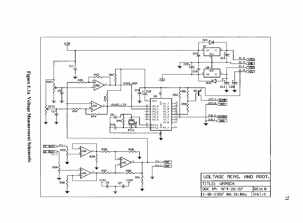
+12V
C14
C11
I R43 R47 1
1 C151.1_
C16
R45 -12U POT1 OVER UTP
C1i tisi8 R51 06
IT_ U6 R52
PST u
POT2
Cli R46
R44
/OVER LTP
I
R 1.9 1
2
3
6
7
8 9
P3_0 P3_I P3_2 P3_3 P3_4 P3_5
'-' PI _7
PI _6
PI _5
P1_4 PI _3
PI _2
PI _I
P1_0
19
18
17
16
15
19
13
12
R50
.5111 .""r 117
5
1 >XTL2 CD P3_7 C>XTLI z
11
XTL1
i
014
U7
i1UO ()I
GND N C1 cp
1
UB GNU
VO VI
015 K1
.7111E0:co
"V
VOLTAGE MEAS. AND PROT. TITLE: UMPSCH
DOC N°: AF4-26-97 REV: B
11-01-1997 06: 31: 06p riSH: 1 /1

72
Table E.1 Voltage Measurement and Protection Component List
REF TYPE VALUE PACKAGE
U4 LM324 quad op amp 14 pin DIP U5 LM339N quad comparator 14 pin DIP U6 89C2051 Atmel flash 8051 20 pin DIP U7 LM7812 +12V regulator TO-220 U8 LM7912 -12V regulator TO-220 XTL1 [LP crystal 12.000MHz std. crystal Q6 2N3906 PNP TO-92 D14-15 1N4002 diode DO-41 C6-8 Z5U cap 0.22p,F 1206 C9-10 NPO cap 33pF 0805 C11 Z5U cap 0.2211F 1206 C12-13 16V electrolytic 100uF polr. can
cap C14 Z5U cap 0.22pY 1206 C15 35V tantalum 2.21AF radial C16-17 Z5U cap 0.22pF 1206 C18 35V tantalum 2.21AF radial C19 Z5U cap 0.22pF 1206 C20 16V electrolytic 100uF radial POT1-2 potentiometer 201d2 7mm pot R33-34 H.V. divider 10MQ (note 2) R35-41 1% chip resistor 101S2 0805 R43-44 chip resistor 1M51 0805 R45-46 chip resistor 1kS1 0805 R47-48 chip resistor 3.3k.0 0805 R49 chip resistor 1MS) 0805 R50 chip resistor 3.3kQ 0805 R51 chip resistor 10kS2 0805 R52 chip resistor 3.3kQ 0805 J15 .156" single hdr 3 pin Connector J16-18 .1" single hdr 2 pin Connector
NOTES:
1. Designations D13 and R42 are not used. 2. R33 and R34 are special high voltage divider networks from Caddock, P/N
1776-C742. The signal is taken off the 100k0 tap, for a ratio of 1:100.

73
J13. 3
J1.5 +24U>
C2 J1.4
GND >
J4.1 X3 IN
J4.2 GND
X4 IN J5.2 P21
GND J11.2
<X 2_C+ I
J11.1 <X2 _C
D9 D10 Dll D12
/> ,cci
o
15
z to N
/\ m)0
N N
AA AA z (nc° °z
o 0 W N
ai 'qv
RELAY CONTROL INTERFACE
TITLE: RLYCTRL
DOC N°: AF4-27-97 REU: B
11-01-1997 06: 46: 40p ISH:1/1
Figure E.lb Relay Control Interface Schematic

r=5=-211-3
P54 P55 P56 R57
016 017 018 019 D20
P58
-14-14-14-14-K-R59
2 U9
C22
J19.1 =ED J19.2 <= J19.3 (ME=
C21
025
026
024
D27
023
D28
D22
029
021
P62
P61 i irOC_NEGATIUE (NOT AT GROUND)
ULT. OVERVOLTAGE PROT. TITLE: ULTOUER
DOC N°: AF4-28-97 [I RDA B 11-01-1997 06: 57:16p SH:1/1
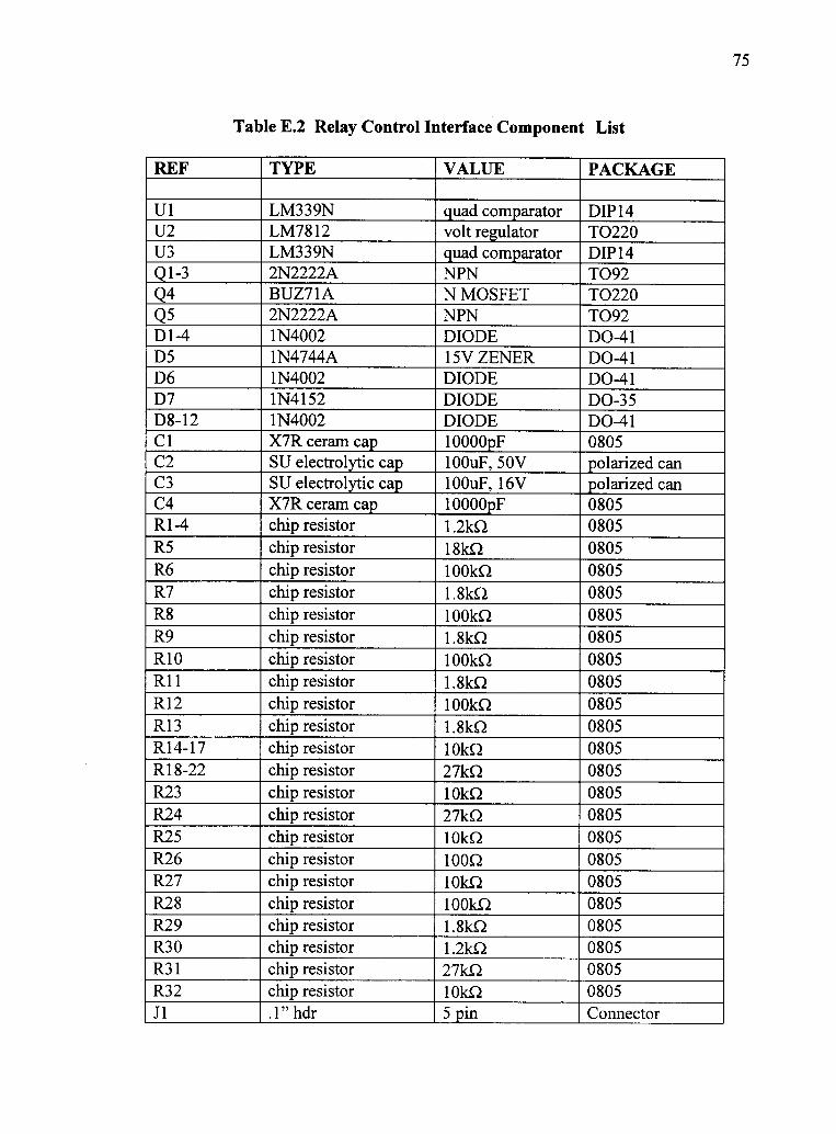
75
Table E.2 Relay Control Interface Component List
REF TYPE
Ul LM339N U2 LM7812 U3 LM339N Q1-3 2N2222A Q4 BUZ71A Q5 2N2222A D1-4 1N4002 D5 1N4744A D6 1N4002 D7 1N4152 D8-12 1N4002 Cl X7R ceram cap C2 SU electrolytic cap C3 SU electrolytic cap C4 X7R ceram cap R1-4 chip resistor R5 chip resistor R6 chip resistor R7 chip resistor R8 chip resistor R9 chip resistor R10 chip resistor R11 chip resistor R12 chip resistor R13 chip resistor R14-17 chip resistor R18-22 chip resistor R23 chip resistor R24 chip resistor R25 chip resistor R26 chip resistor R27 chip resistor R28 chip resistor R29 chip resistor R30 chip resistor R31 chip resistor R32 chip resistor J1 .1" hdr
VALUE
quad comparator volt regulator quad comparator NPN N MOSFET NPN DIODE 15V ZENER DIODE DIODE DIODE 10000pF 100uF, 50V 100uF, 16V 10000pF 1.2k0 18k0 1001M
1.81cS2
100k0 1.81d2
100k0 1.8k0 1001M 1.8k0 101M
27kS-2
101c0
271d2
101M
10052
10k0 1001M 1.81d2
1.21d2
271cS2
10IM 5 pin
PACKAGE
DIP14 TO220 DIP14 TO92 TO220 TO92 DO-41 DO-41 DO-41 DO-35 DO-41 0805 polarized can polarized can 0805 0805 0805 0805 0805 0805 0805 0805 0805 0805 0805 0805 0805 0805 0805 0805 0805 0805 0805 0805 0805 0805 0805 Connector

76
Table E.2 (Continued) Relay Control Interface Component List
REF TYPE VALUE PACKAGE
J2-7 .1" hdr 2 pin Connector J8 .1" hdr 3 pin Connector J9 .1" hdr 2 pin Connector J10-12 .156" hdr 2 pin Connector J13 .156" hdr 3 pin Connector J14 .156" hdr 2 pin Connector
Table E.3 Ultimate Overvoltage Protection Component List
REF TYPE VALUE PACKAGE
U9 HCPL4504 optoisolator 8 pin DIP S6006F1 SCR TO-220Q7
D16-29 1N4751A 30V Zener DO-41 C21 600V poly film 0.11.IF radial
cap C22 Z5U cap 0.22[IF 1206
R53 1/4W resistor 1000 1/4W resistor
R54-R59 1/4W resistor 3.31SI V4W resistor
R60 1/4W resistor 1.01S2 V4W resistor
R61 1/4W resistor 1000 1/4W resistor
R62 1/4W resistor 3000 LAW resistor
Q7 is available from Teccor Corp., of Irving, Texas

77
Overvoltage Protection Fault Monitor Program Code
;fault monitor program, ;Alex Faveluke, 08-21-96 ;disables output driver
.org 0000h
SJMP INIT ;get past IRQ service routine
.org 000Bh ;at timer 0 IRQ vector TIRQSERV: MOV TLO, #19h
MOV THO, #OFCh CPL P3.1 ; should generate square wave
at 500Hz JNB PSW.5, NOINC CLR PSW.5 ;clear the fault flag INC R3 ;inc the integrating register CJNE R3, #OAh, NOINC2 ;if R3=10ms, we've got
problems LJMP SHUTDOWN ;So dissy the buffers...
NOINC: NOP NOP NOP NOP
NOINC2: INC R2 ;always increment integrating timekeeper
CJNE R2, #100D, NOCLR MOV R2, #00h ;clear after 1000ms INC 30h MOV A,#10D CJNE A,30h,NOCLR MOV 30h,#00D MOV R3,#00h ;clear the integrating
register after a sec SJMP NOCLR2
NOCLR: NOP NOP NOP NOP
NOCLR2: RETI
INIT: MOV P1, #11111111b MOV SP, #70h ;can do 7 nested calls

78
Overvoltage Protection Fault Monitor Program Code (Continued)
MOV R2, #00h MOV R3, #00H MOV 30h, #00D
;set up timer MOV TMOD, #00000001b MOV TLO, #19h MOV THO, #OFCh MOV TCON, #00010000b MOV IE, #10000010b CLR P3.0 CLR PSW.5
MAIN: MOV A, P1 ORL A, P1
;timer 0 setup as 16 bit
;start timer ;enable tO IRQ ;enable to 244 buffer ;clear the overi flag
;effectively sample 2 times ;ORL A, #11110000b now should be
all 1 CJNE A, #Offh, OVERT
overcurrent ind. SJMP MAIN
OVERI: SETB PSW.5 SJMP MAIN
SHUTDOWN: SETB P3.0 SJMP SHUTDOWN
;if not, we've got an
;jump back to main
;overcurrent fault indicator.
;disable the 244

79
03 J12 J13 J11 X07
00J1400 a a 04 02 n 08 111 US
U2 a a a 04 U1 J70 17 J9
D90 J1 %12 J3 J4 J5 J6 0 J8
R33
R34
X X X
X C x >c c X X X
X X X
fR53I
U
cm
tm 8501
El
R60
O C
10 I R 6 21
Figure E.2a Voltage Measurement and Protection Board Top Side Component Placement

80
0 0 , 00 000 ,0, ,,,, 0 0 g 0 0 a o°°. °0 0 a OE 0 Mt) 0
000 Ogil 0000000 ,1 00 ZO 0° 0 T o o°°° looaqo '-E2 0 0 go ,3jR oo -;;;J: rmlv, a 00 o Cr''...0;Ltd, LI 't 00 0000
00 ENIa '0000000 -0 M ,;1 CM
0 ifactoo aciaoljao coo CIO 0 0 0
coop 0 0000 000 0 00
0 0 0 0O O 0 00 00 0
0 a o 0 a/217',01,5mO 0 0 0 oo o0 _0 0 0 0 0 0 0 00 00 ;-o0 r'70
00 Fig 000000000 a r--0 o 0 0 0 000-0aFJ do 0 0000000
00 09 0 00000000000o 0 00 0 0 o
o 0 00 0 0000 0000 o .flo o o o o
o or-la orle o a 00000 0 0 0 goGG
O O MIO 0000000 00000010
0 ..-10(3212 0 0ED
000ED 0000 0 0000000 0
CI 0 0 0 0 0 00 o 0 0 0 0 0 0
0 0 0 0 0 0
0 0 Ocacao
0 cocoa o 0 0 00 00 0
0 0 0 0 00 0 0 0 00 0
0 0 0 0 0 0 0 D 0 0
0 ,0000 0 a 0 0 a00 0 0 ° 0
0 0 00 o 000 0 o 0 0 0 0 0 0
0 0 0
0
0
Figure E.2b Voltage Measurement and Protection Board Top Side Component Placement

81
Appendix F. Internal Power Supply Board
The internal power supply board converts the 24 volt output of the line connected
switching supply to +5 and ±15V for the logic and analog supply rails of all logic and
analog hardware. All power supply connections have been made to this board, with
cables carrying ground, +5, +15 15, and +24V. This appendix contains schematics and
component lists, which together completely specify the Internal Power Supply board.

LI
..--... C1 C21 C31 C4
IC1
2
VIN USW
CMP 01 L2
GND F8
L4 1
rmr-__________ CIO
C1112_
5
IC2
UI N
SO
USW
I LM
8
2 D2
L5
P6 C14
+ 00'1
L6/WY\ C16I IL
C12 6 STS SNS 4
C15
3 GND CMP
P7 P13
3 p5 L7
J2.4 ---.< GND
12,3< + u I
L8 J2.2 07160-1
C2 Cl 9
IC3 P9 P11 J2.5 <+24V I
I
5
VIN
SD
USW
I LM
8
2 D3
C21 C22 + C23
..----.. C24 + C25
..--.
J2.1 ( 15V I
6
3
STS SNS
GND CMP
4
7
P10 08
Cl3 P12
L9 \.A...".......1 CONTROL POWER SUPPLY
TITLE: CTRLID1-112
DOC N°: AF6-5-97 [I RDA C 11-01-1997 07:19: 04p SH:1/1

83
Table F.1 Internal Power Supply Component List
REF TYPE
IC1 LT1074 IC2 LT1176 IC3 LT1176 IC4 IC5 IC6 IC7 Q1 TCR6008L D1 MBR1045 D2 IR31DQ06 D3 IR31DQ06 D4 1N4152 D5 1N4730 D6 IR31DQ06 D7 IR31DQ06 D8 IR31DQ06 Ll TORIND1 L2 POTINDI L3 TORINDI L4 TORIND1 L5 TORIND2 L6 TORIND1 L7 TORINDI L8 POTINT2 C1-5 "FA" electro. C6-7 Z5U ceramic C8 electrolytic C9 Z5U ceramic C10 NPO ceramic C11 Z5U ceramic C12 Z5U ceramic C13 X7R ceramic C14 Z5U ceramic C15 "FA" electro. C16 Z5U ceramic C17 electrolytic C18 X7R ceramic C19 Z5U ceramic C20 "FA" electro. C21 NPO ceramic
VALUE
Switcher IC Switcher IC Switcher IC EMPTY PADS EMPTY PADS EMPTY PADS EMPTY PADS SCR SCHOTTKY SCHOTTKY SCHOTTKY SIG DIODE 3.9V Zener SCHOTTKY SCHOTTKY SCHOTTKY 10uH 45uH 10uH 10uH 200uH 10uH 10uH 150uH 390uF, 35V 1.0uF, 50V 100uF 16V 1.0uF, 50V 0.01uF, 50V 1.0uF, 50V 1.0uF, 50V 0.01uF, 50V 1.0uF, 50V 390uF, 35V 1.0uF, 50V 100uF, 16V 0.1uF, 50V 1.0uF, 50V 390uF, 35V 0.01uF, 50V NPO
PACKAGE
5 lead TO220 8 pin DIP 8 pin DIP 8 pin DIP 8 pin DIP 8 pin DIP 8 pin DIP TO220 10220 C-16 C-16 DO-35 DO-41 C-16 C-16 C-16 T80-26 toroid T2213-77 pot core T80-26 toroid T80-26 toroid T80-26 toroid T80-26 toroid T80-26 toroid TI 107 -77 pot core radial radial radial radial disc radial radial axial epoxy dip radial
radial radial axial epoxy dip radial radial disc

84
Table F.1 (Continued) Internal Power Supply Component List
C22 Z5U ceramic C23 "FA" electro. C24 Z5U ceramic C25 electrolytic C26 X7R ceramic R1 resistor R2 resistor R3 resistor R4 resistor R5 resistor R6 resistor R7 resistor R8 resistor R9 resistor R10 resistor R11 resistor R12 resistor
1.0uF, 50V 390uF, 35V 1.0uF, 50V 100uF, 16V 0.01uF, 50V 2.7kQ 5.6kS2
2.2k0 5.6k0 2.21S2
6.8k0 1.2k0 271d2
23.51d1 46.11d2 12.63k0 1.821M
radial radial radial radial axial epoxy dip 1/4W resistor 1/4W resistor 1/4W resistor 1/4W resistor 1/4W resistor 1/4W resistor 1/4W resistor 1/4W resistor 1/4W resistor 1/4W resistor 1/4W resistor 1/4W resistor
Type FA electrolytic capacitors are from Panasonic Corp., availiable through Digi-Key, of Thief River Falls, Minnesota.
Magnetic core components availiable from Amidon, of Torrance, CA
J I is a small pluggable terminal block, with two contacts. J2 -J7 are Molex type 5 pin .156" center headers.

85
11 galMal
J1
01
MCC
L2 06
106
03 LEEN 07 "N 1C7IC1 ) IC5
08 I
111 3 J5 6J2 -111
Figure F.2 Internal Power Supply Top Side Component Placement

86
Appendix G. Photographs
This appendix contains photographs of some of the more critical PC board artwork and the main bus board. The completed converter mounted on a standard rack, surrounded by some of the contributors to this project.

87
Figure G.la Optocoupler Interface, Top Side ofPC Board
Figure G.lb Optocoupler Interface, Bottom Side of PC Board

8S
Figure G.2 Main Bus Board Assembly
The Main Bus Board Assembly includes the IGBT power modules, the
Optocoupler Interfaces, and the Isolating Power Supplies for both the rectifier and the
inverter. The DC link capacitors are mounted directly to the board, implementing a
laminar bus structure described in the text of Chapter 3. Also shown in this photograph
are the cooling fans and heat sink used to transfer thermal energy from the power
modules. The power modules cannot be seen in this view; they mount directly
underneath the Optocoupler Interfaces.

89
Figure G.3 Completed Converter, Rack Mounted and Ready for Use
Pictured here is the completed bi-directional converter. It has been subjected to
extensive testing and operation here at Oregon State University. Surrounding the
converter are some of the contributors to this project; from the left, Brian Koch (outer
loop control development,) Shibashis Bhowmik (inverter and rectifier control software,)
Annabelle Van Zyl (power calculations, thermal design, voltage sag resistance
application development, microcontroller core) Manfred Dittrich (Machinist,) and finally
myself, (low-level analog measurement and control, protection systems design, and
systems integration work.) I would like to take the opportunity to again thank everyone
pictured here for the hard work and cooperation that went into this project. I also would
like to again thank my major professor, Dr. Rene Spee, for the support and guidance that
made all this possible.