Embed Size (px)
Citation preview

Reappraising the Need for Bulk Heterojunctions in Polymer-Fullerene Photovoltaics: TheRole of Carrier Transport in All-Solution-Processed P3HT/PCBM Bilayer Solar Cells
Alexander L. Ayzner, Christopher J. Tassone, Sarah H. Tolbert,* and Benjamin J. Schwartz*Department of Chemistry and Biochemistry and California Nanosystems Institute, UniVersity of California,Los Angeles, Los Angeles, California 90095-1569 USA
ReceiVed: May 30, 2009; ReVised Manuscript ReceiVed: September 15, 2009
The most efficient organic solar cells produced to date are bulk heterojunction (BHJ) photovoltaic devicesbased on blends of semiconducting polymers such as poly(3-hexylthiophene-2,5-diyl) (P3HT) with fullerenederivatives such as [6,6]-penyl-C61-butyric-acid-methyl-ester (PCBM). The need for blending the twocomponents is based on the idea that the exciton diffusion length in polymers like P3HT is only ∼10 nm, sothat the polymer and fullerene components must be mixed on this length scale to efficiently split the excitonsinto charge carriers. In this paper, we show that the BHJ geometry is not necessary for high efficiency, andthat all-solution-processed P3HT/PCBM bilayer solar cells can be nearly as efficient as BHJ solar cells fabricatedfrom the same materials. We demonstrate that o-dichlorobenzene (ODCB) and dichloromethane serve nicelyas a pair of orthogonal solvents from which sequential layers of P3HT and PCBM, respectively, can bespin-cast. Atomic force microscopy, various optical spectroscopies, and electron microscopy all demonstratethat the act of spin-coating the PCBM overlayer does not affect the morphology of the P3HT underlayer, sothat our spin-cast P3HT/PCBM bilayers have a well-defined planar interface. Our fluorescence quenchingexperiments find that there is still significant exciton splitting in P3HT/PCBM bilayers even when the P3HTlayer is quite thick. When we fabricated photovoltaic devices from these bilayers, we obtained photovoltaicpower conversion efficiencies in excess of 3.5%. Part of the reason for this high efficiency is that we wereable to separately optimize the roles of each component of the bilayer; for example, we found that thermalannealing has relatively little effect on the nature of P3HT layers spin-cast from ODCB, but that it significantlyincreases the crystallinity and thus the mobility of electrons through PCBM. Because the carriers in bilayerdevices are generated at the planar P3HT/PCBM interface, we also were able to systematically vary thedistance the carriers have to travel to be extracted at the electrodes by changing the layer thicknesses withoutaltering the bulk mobility of either component or the nature of the interfaces. We found that devices have thebest fill-factors when the transit times of electrons and holes through the two layers are roughly balanced. Inparticular, we found that the most efficient devices are made with P3HT layers that are about four timesthicker than the PCBM layers, demonstrating that it is the conduction and the extraction of electrons throughthe fullerene that ultimately limit the performance of both bilayer and BHJ devices based on the P3HT/PCBM material combination. Overall, we believe that polymer-fullerene bilayers provide several advantagesover BHJ devices, including reduced carrier recombination and a much better degree of control over theproperties of the individual components and interfaces during device fabrication.
I. Introduction
Thin film photovoltaics (PVs) based on blends of conjugatedpolymers as electron donors and fullerenes as electron acceptorshave been the subject of intense research owing to the ease withwhich they can be fabricated into inexpensive plastic solarcells.1-3 When blended together, conjugated polymers andfullerenes phase segregate on nanometer length scales, producinga bicontinuous interpenetrating network of the polymer andfullerene components, which is often referred to as a bulkheterojunction (BHJ).4,5 Light incident on BHJ solar cells isprimarily absorbed by the π-conjugated polymer, leading to thecreation of strongly bound excitons. Literature reports haveestimated that excitons can diffuse only over distances of ∼10nm.6,7 If the polymer and fullerene components are phase-segregated on this same length scale, then essentially every
exciton can diffuse to within charge-transfer range of a fullerenemolecule during its lifetime, resulting in exciton splitting andformation of polaron pairs8-10 with near-unit quantum yield.11-13
These coulombically-bound charge pairs are then separatedbecause of a combination of electric potential and concentrationgradients14 and eventually collected at the electrodes to producea photocurrent in the external circuit. To date, BHJ solar cellsbased on the combination of the regioregular polymer poly(3-hexylthiophene-2,5-diyl) (P3HT) and the fullerene derivative[6,6]-penyl-C61-butyric-acid-methyl-ester (PCBM) have reachedpower conversion efficiencies exceeding ∼5%,15-17 with evenhigher efficiencies obtained for devices based on redder-absorbing conjugated polymers and/or fullerene derivatives.18
Even though polymer-based BHJ solar cells have achievedquite respectable power conversion efficiencies, questions stillremain regarding the fundamental processes that ultimately limitdevice performance. For example, there is still significantargument as to whether the mobility of holes in the polymercomponent or electrons in the fullerene component of the BHJ
* Corresponding authors. (B. J. S.) E-mail: [email protected]. Tel.:(310) 206-4113. Fax: (310) 206-4038. (S. H. T.) E-mail: [email protected].: (310) 206-4767. Fax: (310) 206-4038.
J. Phys. Chem. C 2009, 113, 20050–2006020050
10.1021/jp9050897 CCC: $40.75 2009 American Chemical SocietyPublished on Web 10/27/2009

cell is what limits device performance.19-23 It is well knownthat thermal annealing improves the power conversion efficiencyof polymer-based BHJ photovoltaics, but the effects of annealingon carrier mobility in the individual BHJ components and theway annealing affects the degree of phase segregation also havebeen the subject of debate.19,20 Finally, because BHJs have acomplex, difficult-to-characterize nanoscale morphology,15,24-28
there have been no systematic studies investigating how thetransit times for electrons and holes on the two componentsaffect the general shape of the device current-voltage responseunder solar illumination.
In this paper, we address these fundamental issues inpolymer-fullerene photovoltaic systems by removing thecomplexity associated with the nanoscale architecture of BHJsand focusing on fully solution-cast planar P3HT/PCBM bilayersolar cells. Although the bilayer geometry has not been popularfor polymer-based solar cells on the basis of the argument thatthe smaller interfacial area between the donor and the acceptorin bilayers results in reduced exciton splitting relative to thatin BHJ’s, we find that we still get significant exciton harvestingeven when the polymer component of the bilayer is opticallythick. The facts that exciton splitting in bilayers is still efficientand that segregating the donor and acceptor layers drasticallyreduces bimolecular recombination29 has allowed us to produceall-solution-processed bilayer PV cells with fill-factors reaching70% and power conversion efficiencies in excess of 3.5%.Perhaps more importantly, by separating the layers, we havebeen able to elucidate much of the physics that underlies theoperation of polymer-fullerene solar cells. We find that theincrease in crystallinity of the PCBM component is largelyresponsible for the improvement in power conversion efficiencythat occurs upon thermal annealing. In addition, we have beenable to directly investigate how the difference between theelectron and hole transit times affects the shape of the devicecurrent-voltage curve. We find not only that it is critical tobalance the electron and hole transit times to produce deviceswith optimal efficiency, but also that electron transport in thefullerene component is what limits the performance of bothP3HT/PCBM bilayer and BHJ solar cells.
Beyond understanding the role of the separate componentsand interfaces in polymer-fullerene photovoltaics, we also showin this paper that there are additional advantages to being ableto form bilayer solar-cells cast entirely from solution. First, wedemonstrate that there is a set of so-called orthogonal solventsthat allows sequential spin-coating of polymer and fullerenelayers to produce bilayers: when the right solvent is chosen forspin-casting the fullerene overlayer, there are no changes in thesurface morphology of the polymer underlayer, so that there isa sharp, well-defined interface between the two layers. Thisallows the production of bilayer solar cells with an ease offabrication that rivals that of BHJ devices and significantlysurpasses that of devices in which one of the components mustbe thermally evaporated under high vacuum. The ability to createsolution-processed bilayers also enables the use of organicelectron acceptors that may not survive thermal evaporation.Second, because the two components of bilayer films aredeposited separately, the absorption spectrum and nanometer-scale morphology of both the polymer and the fullerene layerscan be controlled and optimized independently by usingtechniques such as thermal or solvent annealing. Finally,depositing the fullerene top layer from solution offers thepossibility to achieve efficient exciton dissociation withoutadversely affecting the mobilities of the carriers being trans-ported in either the polymer or fullerene layers. Thus, we believe
that these advantages make the bilayer geometry a seriouscontender for the future production of large-scale, efficientpolymer-fullerene-based solar cells.
II. Experimental Section
For the production of bilayer photovoltaic devices, there isan inherent difficulty associated with spin-coating sequentiallayers because most conjugated organic molecules are solublein similar solvents, so that spin-coating a film on top of anorganic underlayer usually results in significant redissolutionof the bottom layer. Thus, bilayer devices are often producedwith one or both layers deposited by thermal evaporation, whichlimits the device area and restricts the choice of active organicmolecules to those that do not decompose during sublimation.One recent alternate approach demonstrated the production ofP3HT/PCBM bilayer solar cells by transferring a PCBM layeronto precoated P3HT substrates by using a poly(dimethylsilox-ane) (PDMS) stamp, resulting in power conversion efficienciesof ∼1.5%.30 Another recent alternate approach involved pho-tocross-linking a derivative of P3HT to render it insoluble, sothat a PCBM overlayer could be spun on top, producing deviceswith power conversion efficiencies of ∼2%.31 In contrast,fabrication of fully solution-processed bilayer cells via spin-coating of both components requires finding a set of so-calledorthogonal solvents32 such that the solvent used to spin-coatthe fullerene overlayers does not affect the morphology of thepolymer underlayers. For P3HT/PCBM devices, we find thatthe common organic solvent dichloromethane (DCM) meets thisrequirement: PCBM is sufficiently soluble in DCM that it ispossible to spin-coat PCBM layers on top of P3HT, and as weshow below, P3HT is so sparingly soluble in DCM that thereis negligible redissolution of the P3HT underlayer during spin-coating of the PCBM overlayer.
We prepared our P3HT/PCBM bilayer solar cells bystarting with prepatterned indium-doped tin oxide (ITO; TFDsales) substrates that were first cleaned by successivesonications in detergent solution, deionized water, acetone, andfinally isopropanol for approximately 10 min each. The sub-strates were then blown dry with Ar and briefly treated with anair plasma (200 mTorr, 10 min) prior to spin-coating a thin (e50nm) poly(ethylenedioxythiophene):poly(styrenesulfonic acid)(PEDOT:PSS, Baytron P VP A1 4083) layer at 5000 rpm for60 s. The PEDOT:PSS-coated slides were then baked on adigitally controlled hot plate in a nitrogen atmosphere for 20min at 140 °C. We prepared solutions of regioregular P3HT(Rieke Metals, 90-93% regioregular) in o-dichlorobenzene(ODCB) at concentrations of 10, 15, 20, 22.5, 25, and 27.5 mg/mL. These solutions were heated to 55 °C for several hours ina nitrogen atmosphere before being cooled to room temperatureand spin-cast onto the PEDOT:PSS-coated substrates at 1000rpm for 90 s, producing P3HT films with thicknesses of 50 (2, 80 ( 2, and 115 ( 2 nm, from the 10, 15, and 20 mg/mLsolutions, respectively, as measured by using a profilometer(Dektak). Thicknesses for films spun from higher-concentrationsolutions were estimated using a thickness vs. optical densitycalibration curve. Freshly-spun P3HT films were allowed to dryin a N2 atmosphere for at least 20 min prior to spin-coating thePCBM overlayer. We then prepared solutions of PCBM (Nano-C) in DCM at concentrations of 5 and 10 mg/mL; the 10 mg/mL solution was briefly heated at 40 °C to ensure maximaldissolution. We found the solubility limit of PCBM in DCM tobe at or just under 10 mg/mL; thus, only the 10 mg/mL solutionwas filtered prior to spin-coating. We then spin-cast the PCBMsolutions at 4000 rpm for 10 s onto the P3HT films from the
P3HT/PCBM Bilayer Solar Cells J. Phys. Chem. C, Vol. 113, No. 46, 2009 20051

previous step, producing PCBM film thicknesses of 22 ( 2 and34 ( 2 nm, respectively. At a rate of less than 5 Å/s, we thenevaporated a cathode consisting of 20 nm of Ca followed by a20 nm Al protective overlayer onto the completed bilayersthrough a shadow mask, resulting in active device areas of 6.5mm2.
We measured the photovoltaic performance of our devicesin an argon atmosphere by using a Keithley 2400 source meter.A xenon arc lamp equipped with a liquid light guide (Oriel)and an AM-1.5 filter was used as the excitation source; theintensity of the incident light on the devices was adjusted to100 mW/cm2, as determined by using a calibrated siliconphotodiode. We calculated a spectral mismatch factor33 for oursetup of nearly unity. To investigate the effects of thermalannealing on device performance, we placed bilayer devicesprior to cathode deposition on a digitally controlled hot plateat 150 °C for 20 min in an Ar atmosphere; the films werecovered with a shallow Petri dish during annealing to helpensure uniform heating. At the end of the 20 min annealingcycle, the films were rapidly cooled by placing them onto aroom-temperature metal surface.
We collected photoluminescence (PL) spectra from ourbilayer films in air at 22.5° with respect to the excitation beamwith the sample positioned at 70° with respect to the excitationaxis. We kept the slit widths and integration times constant forall of our experiments and also normalized all of the PL spectradisplayed by the optical density of the sample at the 530 nmexcitation wavelength and corrected for the detector andmonochromator responses so that the relative intensities of thedifferent PL spectra presented below are meaningful.
Atomic force microscopy (AFM) was carried out by using aNanoscope V Dimension 5000 (Veeco Digital Instruments) inambient conditions. Antimony n-doped silicon cantilevers(TESPW, Veeco Probes) with spring constants of 42 N/m, firstlongitudinal resonance frequencies between 230-410 kHz, andnominal tip radii of 8 nm were employed in tapping mode.Simultaneous height and phase images were acquired andreproduced across multiple samples. To image the P3HTpolymer layer after bilayer fabrication, the PCBM overlayer wasremoved by soaking the bilayer films in cyclohexane (CH) forseveral days in the dark under ambient conditions and thendrying the films under vacuum before performing the measure-ments; as shown below, we found no spectroscopic or AFMevidence for any remaining fullerene following such treatment.
To characterize the PCBM overlayers in our bilayers by X-raydiffraction (XRD), we carried out two-dimensional (2-D) grazingincidence XRD at the Stanford Synchrotron Radiation LightSource on beamline 11-3 with a wavelength of 0.9742 Å. Datawere collected on both pure PCBM films spun from DCM ontosingle-crystal Si substrates and on P3HT/PCBM bilayers. Bothsamples gave similar diffraction data: diffuse low-intensitydiffraction for unannealed films and a series of somewhatsharper peaks in films that had been thermally annealed. Becauseof the very strong P3HT diffraction in the bilayers, however,the PCBM diffraction in the bilayer films was harder to see;thus, we only show the data collected for pure PCBM filmsbelow. Because the 2-D PCBM diffraction images did not showany preferred orientation, we radially integrated the data toproduce the one-dimensional patterns shown below, making iteasier to clearly visualize the degree of crystallinity in each film.
III. Results and Discussion
Although layers of PCBM have been spin-cast from DCMonto P3HT films in the past,34,35 there has been essentially no
work investigating either the quality of the PCBM filmsproduced by spin-coating or the effects of spinning the PCBMtop layer onto the P3HT underlayer. Thus, we begin this sectionwith a detailed examination of the morphology of our spin-castP3HT/PCBM bilayers. We show that the act of spinning pureDCM solvent has a negligible effect on the P3HT underlayer,and that PCBM layers can be deposited and removed withoutsignificantly altering the surface topography of the underlyingP3HT film. We also show that the initially deposited PCBMfilm is largely amorphous, but that the PCBM layer becomespartially nanocrystalline upon thermal annealing. We then turnto study the steady-state photophysics of our P3HT-PCBMbilayers, where PL spectroscopy allows us to investigate thenature of how well PCBM overlayers quench excitons in theP3HT underlayers. We then conclude this section with a detailedinvestigation of the performance of solar cells based on P3HT/PCBM bilayers.
A. Physical Characterization of P3HT/PCBM Solution-Processed Bilayers. One of the real advantages to solution-processed bilayers is that, as long as the two layers are distinctand do not significantly intermix, the morphology and otherproperties of each layer can be studied independently as theprocessing conditions are varied. In this subsection, we show,by using a combination of AFM and optical measurements, thatthe P3HT/PCBM solution-processed bilayers we make have asharp (∼1-nm roughness) interface between the P3HT andPCBM components, a conclusion that is also supported byelectron microscopy images on cross sections of our bilayersthat are presented in the Supporting Information.36 We then usea combination of AFM and XRD to investigate the effects ofthermal annealing on the individual P3HT and PCBM compo-nents of the bilayers and show that the primary effect ofannealing is to increase the crystallinity of the PCBM overlayer.
1. Sharp Interface of P3HT/PCBM Solution-ProcessedBilayers. Because we are preparing our bilayers by spin-castingthe PCBM overlayer from DCM, it is important to ensure thatthe P3HT underlayer is not dissolved or altered by the DCMsolvent used to spin the overlayer. To do this, we started bysimply placing a significant amount of P3HT powder into DCMsolvent. After stirring for several days, the vast majority of thepolymer remained undissolved. The fact that the UV-visibleabsorption of the solution was significantly blue-shifted fromthat of P3HT solutions in good solvents such as ODCB indicatesthat only a small amount of low-molecular-weight and/orregiorandom material had dissolved in the DCM. After severalwashes, we found that DCM solvent left in contact with P3HTpowder was only very faintly colored. Thus, we can concludethat, with the possible exception of regiorandom impurities orsome very-low-molecular-weight material, regioregular P3HTis essentially insoluble in DCM. In the spectroscopic data shownbelow, we prepared the film samples by using the DCM-washedP3HT powder; however, we found that the performance of ourbilayer solar cells did not depend on whether the P3HT powderwas washed in DCM.
To verify that the use of DCM solvent for deposition of thePCBM overlayer does not affect the morphology of the P3HTunderlayer, we present tapping-mode AFM phase images of theinitially deposited P3HT layer as it undergoes the several stepsof processing needed to fabricate a bilayer in Figure 1. An imageof the surface of a film of pure P3HT cast from ODCB is shownin Figure 1A. The film’s surface is composed of rice-likenanoscale crystallites with an average diameter of 13.8 ( 2.4nm. To test the effects of spinning an overlayer from a differentsolvent onto the P3HT film, we spin-cast a drop of pure DCM
20052 J. Phys. Chem. C, Vol. 113, No. 46, 2009 Ayzner et al.
onto the P3HT film and remeasured the AFM tapping-modephase image, shown in Figure 1B. The data make it clear thatthe morphology of the P3HT underlayer is maintained in thepresence of DCM; the average P3HT crystallite diameterremains essentially unchanged at 13.2 ( 2.4 nm. Spinning DCMsolvent onto the P3HT layer also has a negligible effect on thesurface roughness of the P3HT film: the root mean square (rms)surface roughness changes from 1.55 to 1.47 nm upon additionof the spin-cast DCM drop, a difference that is within the batch-to-batch variations we observed over multiple measurements.Thus, we can conclude that the addition of DCM does not causeany detectable differences in the surface morphology of P3HTfilms.
To further verify that creating a bilayer by spin-casting asolution of PCBM in DCM on top of P3HT does not alter themorphology of the underlying P3HT film, we fabricated a P3HT/PCBM bilayer and then removed the PCBM overlayer bysoaking the bilayer in CH for several days; a tapping-mode AFMphase image of the P3HT layer that remained following removalof the PCBM overlayer is shown in Figure 1C. Like with spin-casting a pure DCM drop, spin-casting a PCBM overlayer andthen removing it has little effect on the underlying P3HT surfacemorphology: the diameter of the crystalline grains are 14.00 (1.8 nm, which is unchanged within the error of the measurement.
The surface roughness of the P3HT film, on the other hand,does increase slightly to 2.47 nm upon addition and removal ofthe PCBM overlayer. A comparison to the surface topographyof an as-cast P3HT film that had been soaked in CH (withoutfirst spin-casting a PCBM overlayer), however, shows a nearlyidentical topography. These results suggest that the smallincrease in surface roughening seen via AFM comes fromsoaking the bilayer in CH and that the act of spin-coating thePCBM overlayer from DCM negligibly changes the underlyingP3HT film morphology. This conclusion is also supported bythe electron-microscopy results presented in the SupportingInformation,36 which show that the thickness and surfaceroughness of the P3HT layer do not change after overcoatingwith PCBM to produce a bilayer.
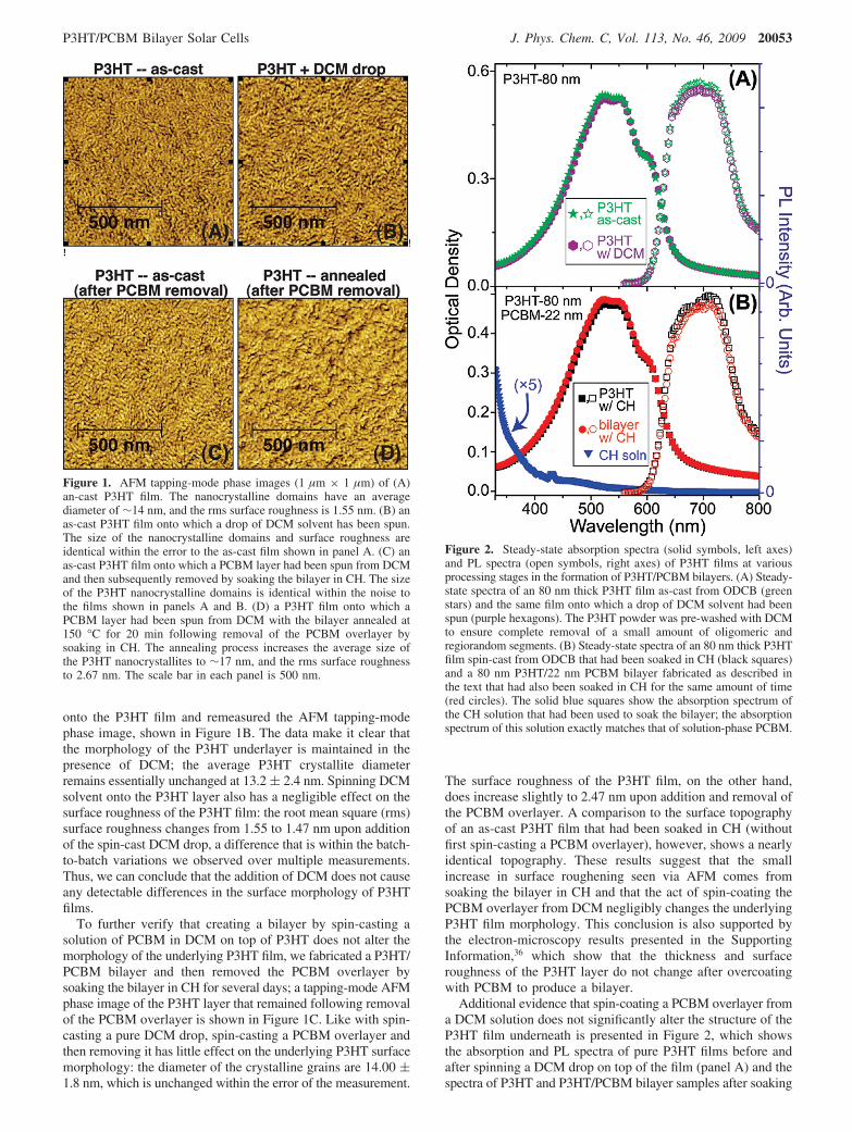
Additional evidence that spin-coating a PCBM overlayer froma DCM solution does not significantly alter the structure of theP3HT film underneath is presented in Figure 2, which showsthe absorption and PL spectra of pure P3HT films before andafter spinning a DCM drop on top of the film (panel A) and thespectra of P3HT and P3HT/PCBM bilayer samples after soaking
Figure 1. AFM tapping-mode phase images (1 µm × 1 µm) of (A)an-cast P3HT film. The nanocrystalline domains have an averagediameter of ∼14 nm, and the rms surface roughness is 1.55 nm. (B) anas-cast P3HT film onto which a drop of DCM solvent has been spun.The size of the nanocrystalline domains and surface roughness areidentical within the error to the as-cast film shown in panel A. (C) anas-cast P3HT film onto which a PCBM layer had been spun from DCMand then subsequently removed by soaking the bilayer in CH. The sizeof the P3HT nanocrystalline domains is identical within the noise tothe films shown in panels A and B. (D) a P3HT film onto which aPCBM layer had been spun from DCM with the bilayer annealed at150 °C for 20 min following removal of the PCBM overlayer bysoaking in CH. The annealing process increases the average size ofthe P3HT nanocrystallites to ∼17 nm, and the rms surface roughnessto 2.67 nm. The scale bar in each panel is 500 nm.
Figure 2. Steady-state absorption spectra (solid symbols, left axes)and PL spectra (open symbols, right axes) of P3HT films at variousprocessing stages in the formation of P3HT/PCBM bilayers. (A) Steady-state spectra of an 80 nm thick P3HT film as-cast from ODCB (greenstars) and the same film onto which a drop of DCM solvent had beenspun (purple hexagons). The P3HT powder was pre-washed with DCMto ensure complete removal of a small amount of oligomeric andregiorandom segments. (B) Steady-state spectra of an 80 nm thick P3HTfilm spin-cast from ODCB that had been soaked in CH (black squares)and a 80 nm P3HT/22 nm PCBM bilayer fabricated as described inthe text that had also been soaked in CH for the same amount of time(red circles). The solid blue squares show the absorption spectrum ofthe CH solution that had been used to soak the bilayer; the absorptionspectrum of this solution exactly matches that of solution-phase PCBM.
P3HT/PCBM Bilayer Solar Cells J. Phys. Chem. C, Vol. 113, No. 46, 2009 20053

in CH (panel B). Figure 2A shows that neither the absorptionnor the PL of a P3HT film is affected by spin-coating a drop ofDCM solvent on top of the P3HT film, a result consistent withthe AFM and electron microscopy36 data discussed above. Figure2B shows that after soaking both a pure P3HT film and a P3HT/PCBM bilayer in CH for several days, the PL intensity of theformer bilayer film is identical within error to that of the pureP3HT film, indicating that our soaking procedure has effectivelyremoved all of the PCBM from the bilayer. We also see thatthe solvent used to soak the bilayer exhibits the solution-phasespectrum of PCBM. The fact that both the optical andtopographic properties of P3HT films are virtually unaffectedby spin-coating the PCBM overlayer provides consistentevidence that the P3HT/PCBM interface in our bilayer samplesis relatively sharp.
Finally, Figure 3 presents the results of experiments that verifythat if interdiffusion of PCBM into the P3HT underlayer hadoccurred during formation of the bilayer, we would have seenclear signatures of this via AFM. Figure 3A shows a tapping-mode AFM phase image of an 80 nm thick 1:1 w/w P3HT:PCBM BHJ film spin-cast from ODCB. The rice-grain-likestructure that is seen at the surface of films of pure P3HT (cf.Figure 1) is suppressed because the presence of PCBM in thefilm breaks up the nanoscale crystallinity of the P3HT. The darkfeatures in this phase image, which correspond to bumps intopography, indicate that PCBM-rich domains are present atthe top surface of the BHJ film.37 The fact that the rice-grain-like structure at the surface of the P3HT underlayers in ourbilayers is still clearly visible following deposition and removalof the PCBM overlayer (Figure 1C) is thus additional evidencethat PCBM did not diffuse into the P3HT underlayer. Moreover,Figure 3B shows an AFM phase image of an P3HT:PCBM BHJfilm that had had a drop of pure DCM solvent spun on top ofit; other than the DCM drop, this BHJ film was preparedidentically to the one shown in Figure 3A. Because PCBM ishighly soluble in DCM, the act of spin-coating DCM onto theBHJ blend film removes a significant fraction of the PCBM, asverified by absorption and PL spectroscopy similar to that shownabove in Figure 2. The removal of PCBM leaves large craters
and valleys in the surrounding P3HT matrix that are clearlyvisible in the AFM image and result in a ∼5 fold increase inthe surface roughness of the film. Thus, the data in Figure 3verify that there would have been obvious topographic signaturesif PCBM had significantly interdiffused into the P3HT under-layer during the bilayer fabrication process; therefore, we canbe confident that the P3HT/PCBM bilayers we produce have arelatively sharp interface between the two components.
2. Effects of Thermal Annealing on the Morphology ofP3HT/PCBM Bilayers. Now that we have established that theP3HT/PCBM interfaces in our solution-processed bilayer samplesare fairly sharp, we can use AFM to examine the changes inP3HT surface morphology induced by thermal annealing. If wespin-cast a P3HT film from ODCB and then thermally annealit, we see that the diameter of the crystalline grains increasesslightly to ∼17 nm (not shown), a result in agreement withprevious reports in the literature.38 If we then spin-coat a PCBMoverlayer onto the P3HT film, anneal the full bilayer, and thenremove the PCBM overlayer by soaking in CH, we recover analmost identical annealed P3HT surface morphology, as shownby the AFM tapping-mode phase image in Figure 1D. Thisindicates that other than thermal annealing, none of theprocessing procedures we employ in the fabrication of oursolution-processed bilayers affects either the surface morphologyor the intrinsic chain packing in the P3HT underlayer and thatannealing does not promote intermixing of the two componentsor alter the intrinsic flatness of the P3HT/PCBM interface.
Now that we know that thermal annealing does not affectthe layer structure of our solution-processed bilayers, we canturn to investigate the effects of different processing steps onthe morphology of the PCBM overlayer. Figure 4A shows anAFM phase image of the top surface of a ∼22 nm thick PCBMoverlayer that was spin-cast from DCM onto a P3HT underlayer.The image is almost perfectly homogeneous, indicating that thefilm is very flat; the rms surface roughness is only 0.46 nm.The lack of discernible features also shows that the PCBM filmis largely amorphous: we would expect a partially crystallineor polycrystalline material to show phase contrast acrosscrystalline domain boundaries because of the difference in forcemodulus at the edges of the domains, as observed for the P3HTunderlayer. In contrast, Figure 4B shows that the surfacetopography of the PCBM overlayer changes upon thermalannealing, with discernible nanoscale crystallites appearing inthe annealed bilayer. The PCBM nanocrystallites are needle-like, with an average length of 43.11 ( 18.12 nm and an averagewidth of 8.72 ( 1.63 nm, and sit in a background of largelyamorphous material. Thus, we can conclude that spin-castPCBM layers are highly amorphous and that thermal annealinginduces partial crystallinity in pure PCBM films.
In order to confirm that the topographic features shown inFigure 4B are truly PCBM nanocrystallites, in Figure 4C, weshow the results of XRD measurements of both as-cast andthermally annealed spin-coated PCBM films. The blue dottedcurve shows that only a weak diffraction peak is observable,centered at 13.8 nm-1, for the as-cast PCBM film, confirmingthat the as-cast film is primarily amorphous in nature. Uponthermal annealing, the red solid curve shows three distinct peaksat 12.5, 13.9, and 14.7 nm-1. On the basis of the widths ofthese peaks, the Scherrer equation39 gives an estimate for theaverage diameter of the crystallites of ∼20 nm, which is inexcellent agreement with the average size of the nanoscalefeatures seen via AFM. The exact assignment of the thermallyannealed PCBM diffraction peaks is somewhat difficult to makebecause there are a number of peaks near these positions in the
Figure 3. AFM tapping-mode phase images (1 µm × 1 µm) of (A)an 80 nm thick 1:1 w/w P3HT:PCBM BHJ blend film spin-cast fromODCB. The nanocrystalline P3HT domains seen in Figure 1 aresuppressed by the presence of PCBM at the top surface of the film,which breaks up the order of the P3HT chains. The large black features,which correspond to bumps in topography, result from PCBM-richdomains. (B) The same BHJ film shown in panel A onto which a dropof pure DCM solvent had been spun. The new features and ∼5 foldincrease in surface roughness result from the removal of PCBM fromthe blend film by the DCM solvent, leaving behind an open P3HTmatrix. These results show clearly that if the PCBM in bilayer structureshad interdiffused into the P3HT underlayer, it would have resulted inobvious signatures via AFM.
20054 J. Phys. Chem. C, Vol. 113, No. 46, 2009 Ayzner et al.

various PCBM crystal structures obtained from the family ofpolymorphs reported for PCBM crystals grown from differentsolvents.40 Whatever the precise assignment, the data in Figure4 confirm that spin-cast films of PCBM are quite amorphousand that thermal annealing increases the degree of PCBMcrystallinity.
B. Photophysics of Solution-Processed P3HT/PCBM Bi-layers. With an understanding of the role thermal annealingplays in the structure of our well-defined bilayers, we turn inFigure 5 to examine the photophysics of our bilayer films. Theblack squares in Figure 5 show the steady-state PL spectrumof an as-cast 80 nm thick P3HT film spun from ODCB. Therelatively pronounced PL shoulder near 720 nm, along with thehighly structured absorption spectrum and red absorption peaknear 600 nm seen in Figure 2, have been attributed by othersas resulting from a high degree of order of the P3HT chains inthe film.41 This is consistent with our choice of ODCB as thesolvent used for spin-coating:42,43 the slow evaporation kineticsof ODCB gives the polymer chains more time to aggregate, inaccord with the AFM images shown in Figure 1 that verify thatthe P3HT is highly nanocrystalline. The production of suchP3HT aggregrated lamellar phases by slow solvent evaporationor thermal annealing is advantageous for solar-cell operationbecause more ordered P3HT chains are associated with higherhole mobilities.24,44 We note that the absorption spectrum ofP3HT films spun from ODCB changes little upon thermalannealing at 150 °C for 20 min (not shown), consistent withliterature reports:45 the slow solvent evaporation of OCDB leavesP3HT films spun from this solvent in an essentially annealed
state. We also note that the residual PL from P3HT:PCBM BHJblend films spun from ODCB does not display the structureindicative of this high degree of organization because the largeamounts of PCBM in such films inhibit ordering of the P3HTchains,46 consistent with the AFM image shown in Figure 3A.And as discussed above, we saw significant changes in neitherthe shape nor the intensity of the absorption spectrum of theP3HT layer following deposition of the PCBM overlayer (Figure5, inset), either before or after thermal annealing.
The red circles in Figure 5 display the spectroscopy of anas-cast bilayer with an 80 nm thick P3HT underlayer and a ∼22nm thick PCBM overlayer collected under the same conditionsas for the pure P3HT film; the layer thicknesses were verifiedby profilometry. The absorption spectrum of this bilayer, shownin the inset, fits perfectly to the sum of the individual P3HTand PCBM absorption spectra. The PL data in the main panelshow clearly that deposition of the thin PCBM overlayer resultsin highly quenched polymer fluorescence: comparison of thespectrally integrated PL from the bilayer and from the P3HTfilm with no PCBM overlayer yields a quenching ratio of ∼90%.We note that steady-state PL quenching measurements arefrequently plagued by thin-film interference effects and/or wave-guiding of the fluorescent light.47 Although we cannot fullyeliminate these effects, we believe they have been minimizedby choosing a ∼20 nm thickness for the PCBM overlayer inthese experiments, which is so small compared to the wave-length of the emitted light that the presence of the overlayershould not alter any interference or waveguiding effects in theP3HT underlayer. The ∼90% quenching ratio implies a verylong effective P3HT exciton quenching length: because the 80nm thick P3HT underlayer is photoexcited from the bottom,this result implies an effective quenching length of ∼80 nm.This is surprising given that the exciton diffusion length hasbeen estimated by several groups to be in the range of 8-20
Figure 4. (A) AFM tapping-mode phase image (1 µm × 1 µm) of anas-cast PCBM overlayer spin-cast from DCM on top of a P3HT film.The lack of phase contrast and the 0.46 nm rms surface roughnessindicate that the film is largely amorphous. (B) AFM tapping-modephase image (1 µm × 1 µm) of a PCBM overlayer spin-cast from DCMon top of a P3HT film after the bilayer had been thermally annealed at150 °C for 20 min. Annealing produces PCBM nanocrystallites withan average diameter of ∼26 nm and increases the rms surface roughnessof the film to 2.34 nm. (C) XRD of PCBM films spin-cast from DCMboth before (blue dashed curve) and after (red solid curve) thermalannealing. The appearance of the diffraction peaks after annealing isconsistent with the observation of PCBM nanocrystallites in panel B;the width of these peaks corresponds to an average crystalline domainsize of ∼20 nm, also in excellent agreement with the AFM results inpanel B.
Figure 5. Steady-state PL spectra following 530 nm excitation for an80 nm thick P3HT film spin-cast from ODCB that had had a drop ofpure DCM solvent spun on top of it (black squares), a solution-processed bilayer with an identical P3HT underlayer and a 22 nmPCBM overlayer spin-cast from DCM (red circles), and the same bilayerfollowing thermal annealing (green triangles). The spectrally integratedPL quenching of the as-cast P3HT/DCM film upon addition of thePCBM overlayer is ∼90%. The inset shows the absorption spectrumof the bilayer prior to thermal annealing.
P3HT/PCBM Bilayer Solar Cells J. Phys. Chem. C, Vol. 113, No. 46, 2009 20055

nm.6,7,48 We will show in an upcoming paper49 that this unusuallyhigh PL quenching of thick P3HT films by thin PCBMoverlayers results from a novel long-range exciton quenchingmechanism.50,51
The green triangles in Figure 5 show that upon thermalannealing, the PL intensity from P3HT/PCBM bilayers under-goes a slight increase, indicating a decrease in exciton quenchingefficiency. This result is in direct contrast to the work of Dreeset al., who observed that thermal annealing led to increasedquenching of the PL from interdiffused blends of a poly(phe-nylene vinylene) derivative and C60.52 These authors attributedthis increased quenching as resulting from increased mixing ofthe polymer and fullerene components induced by thermalannealing. The fact that thermally annealing our bilayer samplesresults in decreased exciton quenching suggests that annealingdoes not promote intermixing of the two components in oursolution-processed bilayers.19 Thus, the behavior of the PL seenin Figure 5, in combination with the data in the previous section,provides consistent evidence that our solution-processed bilayershave a relatively sharp polymer-fullerene interface whether ornot they are thermally annealed.
C. Performance Characteristics of Solution-ProcessedP3HT/PCBM Bilayer Photovoltaics. With an understandingof the morphological and photophysical properties of oursolution-processed bilyers in hand, we turn next to the behaviorof photovoltaic devices in which these bilayers serve as theactive medium. We fabricated bilayer devices with differingP3HT and PCBM layer thicknesses and different annealingconditions, the performance characteristics of which are sum-marized in Table 1. The solar-cell performance characteristicspresented in this table represent average values obtained bytesting multiple films with three devices per film. We find anapproximately 5% error in Jsc and Voc and roughly a 10% errorin FF. Only devices that showed good diodic behavior in thedark were included in the averaging. The injected-currentcharacteristics of some of our bilayer devices are shown in theSupporting Information; if we assume that the current injectedis space-charge limited, we extract an average carrier mobilityfor our devices of 2.3 × 10⁻⁵ cm2V-1s-1.36
1. Effects of Thermal Annealing on Bilayer Solar Cells.Figure 6 shows the performance characteristics of ITO/PEDOT:PSS/80 nm P3HT/22 nm PCBM/Ca sandwich-structure bilayersolar cells where the active bilayer was either as-cast (blackupward triangles) or thermally annealed before deposition ofthe Ca cathode (filled blue downward triangles). The data inthis figure and Table 1 make it clear that thermally annealing
completed P3HT/PCBM bilayer solar cells prior to Ca deposi-tion dramatically improves the device performance relative toas-cast devices: annealing causes an increase in Jsc of ∼23%and in FF of ∼74% relative to the as-cast device. In addition,annealing produces an increase in the Voc of these bilayer cellsby nearly 15%, which is surprising given that annealing hasbeen shown to have relatively little effect on the Voc of BHJcells fabricated from these same materials.20,53 We are confidentthat these annealing-induced changes in the performance of thebilayer cells do not result from changes in the morphology ofthe P3HT layer for two reasons. First, we saw very little changein the P3HT absorption spectrum or surface topography uponannealing, suggesting that thermal annealing does little to changethe degree of chain ordering in the highly organized P3HT layerthat was cast from ODCB.45 Second, we also prepared bilayersolar cells in which we annealed the P3HT underlayer before
TABLE 1: Performance Parameters of ITO/PEDOT:PSS/P3HT/PCBM/Ca/Al Bilayer Solar Cells Under AM-1.5 Illumination
Processing of SolarCell Active Bilayer P3HTa (nm) PCBMa (nm) Jsc (mA cm-2) Voc (V) FF (%) PCEb (%)
annealed 50 22 6.9 0.66 68 3.1as-cast 80 22 6.1 0.58 39 1.4annealed P3HT onlyc 80 22 5.4 0.38 38 0.8annealed 80 22 7.5 0.66 68 3.4annealed 115 22 6.2 0.66 53 2.2annealed 125 22 6.9 0.67 54 2.5annealed 140 22 6.0 0.66 45 1.8annealed 155 22 4.6 0.66 40 1.2annealed 50 34 3.3 0.63 52 1.1annealed 80 34 5.9 0.63 68 2.5annealed 115 34 8.2 0.63 66 3.5annealed 125 34 8.3 0.64 64 3.4annealed 140 34 8.6 0.64 63 3.5annealed 155 34 8.7 0.65 61 3.4
a Thickness of the spin-cast layer. b Power conversion efficiency. c P3HT layer was annealed before deposition of the PCBM overlayer.
Figure 6. Current density versus applied bias for ITO/PEDOT:PSS/P3HT/PCBM/Ca/Al solution-processed bilayer solar cells under AM-1.5 illumination, where the active bilayer is either an as-cast ∼80 nmthick P3HT film spin-cast from ODCB with a 22 nm thick PCBMoverlayer spun from DCM (solid black upward triangles) or an ∼80nm thick P3HT film with a DCM-spun ∼22 nm PCBM overlayer thathad been thermally annealed at 150 °C for 20 min prior to depositionof the cathode (solid blue downward triangles). For comparison, theopen blue downward triangles show the J-V characteristics of anidentical bilayer device where the P3HT layer was annealed prior todeposition of both the PCBM overlayer and the cathode. Details of thedevice performance parameters are summarized in Table 1.
20056 J. Phys. Chem. C, Vol. 113, No. 46, 2009 Ayzner et al.

spin-coating the PCBM overlayer, and we found that theperformance of these devices decreased relative to those inwhich neither layer was annealed, as shown by the open bluedownward triangles in Figure 6. Thus, the thermal annealing-induced improvement in performance of our bilayer devices ismost likely due to changes that occur within the fullerene layer.
We believe that the performance improvements that occurin bilayer devices that were thermally annealed result primarilyfrom the annealing-induced increase in crystallinity of thefullerene overlayer (cf. Figure 4). This is because the morphol-ogy of the as-cast fullerene layer is largely amorphous, aconsequence of kinetic trapping of the interfullerene packingstructure due to the rapid evaporation of DCM during spin-coating. The amorphous nature of this layer results in a largedegree of positional and energetic disorder, which is correlatedwith slow electron-hopping rates and thus poor electron mobility.The partial crystallization of PCBM that occurs upon annealingremoves some of this disorder, producing an increased electronmobility and hence an increased photocurrent. The increasedelectron mobility also decreases the average transit time (ttr)for the electrons to traverse the fullerene layer.54 As discussedfurther below, we believe that the annealing-induced improve-ment in fill-factor is a direct consequence of an improvedbalance of the carrier transit times for the electrons and holesin the bilayer device.
2. Effects of Layer Thickness on the Performance of BilayerSolar Cells. The data in the previous section argue stronglythat electron mobility in the PCBM layer plays a significantrole in determining the shape of the current-voltage curve ofsolution-processed P3HT/PCBM bilayer solar cells. To betterunderstand the roles of electron mobility and perhaps mostimportantly the balance of carrier transit times on deviceperformance, we have measured the operating characteristicsof bilayer solar cells as a function of the thickness of theindividual P3HT and PCBM layers, as summarized in Figure 7and Table 1. Because all of the carriers in bilayer photovoltaicsare generated within a few nanometers of the donor-acceptorinterface, our ability to vary the thickness of the individual layersallows us to study how changing the transit time of each carrieraffects solar cell performance without significantly changingthe bulk mobility of either component or the nature of theinterfaces. This is something that is not possible with BHJdevices, where changes in the nanometer-scale morphology ofthe interpenetrating network of the two components withprocessing conditions1,4 make it impossible to determine thedistance carriers must traverse to exit the device or to keep themobility of one carrier virtually fixed while varying the mobilityof the other carrier via thermal annealing.
Figure 7A shows the AM-1.5-illuminated current-voltagecharacteristics of P3HT/PCBM bilayer solar cells annealedbefore deposition of the Ca cathode with three different P3HTlayer thicknesses: 50 nm (green diamonds), 80 nm (bluetriangles), and 115 nm (red squares). The PCBM layer thicknesswas held fixed at 22 nm for all of these devices. The data showthat the photovoltaic power conversion efficiency does notchange monotonically with P3HT layer thickness: the efficiencyof the devices with 80 nm thick P3HT layers is higher thanthose of the devices with thicker and thinner P3HT layers. Webelieve that this P3HT thickness dependence of the deviceperformance results from a trade-off between improved opticalabsorption and misbalanced carrier transit times54 as thethickness of the P3HT layer is increased. The devices with 50nm thick P3HT layers have the highest fill-factor, suggestingthat the carrier transit times in these cells are the closest to being
optimally balanced. The overall efficiency of these devices isthus likely limited only by photon harvesting, because the thin50 nm polymer layer has an optical density at the P3HT
Figure 7. (A) Current density versus applied bias for thermallyannealed ITO/PEDOT:PSS/P3HT/PCBM/Ca/Al solution-processed bi-layer solar cells under AM-1.5 illumination with a 22 nm thick PCBMoverlayer for different thicknesses of the P3HT underlayer spun fromODCB: 50 nm (green diamonds), 80 nm (blue triangles), and 115 nm(red squares). (B) The same as panel A but for devices with a 34 nmthick PCBM overlayer spun from DCM. (C) Bilayer-solar-cell perfor-mance factors as a function of P3HT layer thickness. The squares showthe performance of devices with a 22 nm thick PCBM layer, whereasthe circles show the performance of devices with a 34 nm thick PCBMlayer. Solid symbols denote the device fill-factor (left axis), whereasopen symbols denote the device short-circuit current (right axis). Linesconnecting the data points are meant to guide the eye. Details of thedevice performance parameters are summarized in Table 1.
P3HT/PCBM Bilayer Solar Cells J. Phys. Chem. C, Vol. 113, No. 46, 2009 20057

absorption maximum of only ∼0.35. When the thickness of theP3HT layer is increased to 80 nm, the Jsc increases becausethe larger absorption by the thicker polymer layer leads to thecreation of additional carriers. The fill-factor of the 80 nm thickP3HT devices is slightly lower than those of the 50 nm devices,however, suggesting that the increased hole transit time associ-ated with the thicker P3HT layer is becoming out of balancewith the smaller electron transit time in the thin PCBM layer.When the device thickness is further increased to 115 nm, eventhough the absorption is further increased, the hole transit timebecomes so out of balance with the electron transit time thatthe FF decreases considerably, and the Jsc is significantlyreduced. Another possible explanation for the poor performanceof this device is that the 115 nm thick polymer layer has becomemuch larger than the effective quenching length, limiting excitonharvesting and thus device efficiency. The PL quenching datain Figure 5, however, suggest that exciton harvesting is not aproblem in our bilayer samples.51 We will show next that it isindeed misbalanced carrier transit times that limit the perfor-mance of bilayer devices with thick P3HT layers.
If misbalanced carrier transit times are really the main culpritlimiting the fill-factor in P3HT/PCBM bilayer solar cells withthick P3HT layers, then it should be possible to improve deviceswith thick P3HT layers by increasing the thickness of the PCBMlayer to improve the balance. Figure 7B shows the photovoltaicperformance of a set of P3HT/PCBM bilayer solar cellsfabricated under conditions identical to those in Figure 7Aexcept that the PCBM overlayer thickness was increased from22 to 34 nm. The simple act of increasing the PCBM layerthickness leads to a completely different trend of the powerconversion efficiency with P3HT layer thickness: with the 34nm thick PCBM overlayer, it is the devices made with 115 nmthick P3HT layers (solid red squares) that have by far the bestpower conversion efficiency, despite the fact that one mightexpect there to be poor diffusion of the P3HT excitons to thePCBM interface through such a thick layer of P3HT.6 In fact,these devices have a higher Jsc than any of the devices with the22 nm thick PCBM layer shown in Figure 7A, including thedevices with 80 nm thick P3HT layers (solid blue triangles),and have power conversion efficiencies that exceed 3.5%. Thefact that the 115 nm P3HT/34 nm PCBM bilayer devices havea higher current, a similar FF, and a higher efficiency thancomparable devices in which both layers are thinner indicatesthat it is balancing the carrier transient timessnot simplyminimizing themsthat is important for the optimization ofpolymer-fullerene solar cells. The devices in Figure 7B withthinner P3HT layers thus suffer from both a reduced absorptionand a more misbalanced set of carrier transit times, explainingtheir lower net power conversion efficiency.55 We show in theSupporting Information that the effective mobility of the carriersinjected into bilayers in the dark is also improved when thecarrier transit times are balanced, even when the total devicethickness has to be increased to achieve this balance.36
Figure 7C and Table 1 summarize how both the fill-factor(filled symbols) and the short-circuit current (open symbols) ofour bilayer devices vary with P3HT thickness for bilayers withboth 22 nm (blue squares) and 34 nm (red circles) PCBMoverlayers. Because the open-circuit voltage is nearly the samefor all of these devices, the device efficiencies are proportionalto the product of the short-circuit current and the fill-factor(Table 1). This figure shows clearly how the fill-factor reachesa maximum when the P3HT thickness is chosen to match thecarrier transit times in the two layers, as discussed above. Butperhaps the most striking feature of the data in Figure 7C is
that for the devices with the 34 nm thick PCBM overlayer, theshort-circuit current continues to increase with P3HT layerthickness, even for P3HT layers as thick as 150 nm. This againindicates that exciton harvesting is not what limits the perfor-mance of our bilayer devices and suggests that we could makeeven more efficient bilayer devices if we were able to spin-coat PCBM layers that were thicker than 34 nm.
The other important feature of the data in Figure 7 is that fora given PCBM overlayer thickness, the optimally efficientbilayer solar cell is the one with a P3HT layer that is aboutfour times thicker than the PCBM layer. Because the distancethe holes must travel to be extracted is four times that of theelectrons, this strongly indicates that the mobility of the electronsin the PCBM layer is smaller than that of the holes in the P3HTlayer: in other words, it is the conduction and/or extraction ofelectrons that ultimately limits the performance of these devices.We believe that the mobility of electrons in the PCBM layer isthe limiting factor because bilayer devices with annealed PCBMlayers work better than bilayer devices with as-cast PCBMlayers, independently of the state of the P3HT layer (Figure 6,Table 1). We also have argued in previous work that it iselectron conduction among the fullerene component of P3HT:PCBM BHJ devices that is performance-limiting;19 thosearguments are reinforced by the data given here. In other words,the BHJ geometry forces electrons to travel a longer, moretortuous path on a PCBM network that is much less crystallinethan is the case in our annealed bilayer devices. Because theBHJ geometry involves an interpenetrating network, the fullerenethickness cannot be adjusted independently of the polymerthickness as it can in the bilayer geometry. Thus, these resultsimply that the most fruitful avenues for investigating how tofurther improve polymer-fullerene solar cells lie in improvingcarrier mobility in the fullerene component, not the polymercomponent, of the devices.56
IV. Conclusions
In summary, we have prepared fully solution-cast P3HT/PCBM bilayer solar cells with well-defined planar interfacesand found that their photovoltaic performance rivals that of BHJdevices fabricated from the same materials. We found thatODCB and DCM serve as an excellent pair of orthogonalsolvents for the sequential spin-coating of regioregular P3HTand PCBM layers, respectively, and that spinning the PCBMoverlayer has essentially no effect on the morphology of theP3HT underlayer. The ease of solution processing not onlyprovides a general method for fabricating bilayer devices frommaterials that do not survive thermal deposition but also allowsthe performance of each layer to be optimized (e.g., via thermalannealing or use of solvent additives) individually, somethingthat is not possible for devices based on the BHJ architecture.
Our choice to fabricate bilayer P3HT/PCBM devices is basedon the fact that their geometry is much simpler than the complexnanometer-scale architecture inherent in BHJ devices. Inparticular, the nature of the interpenetrating network in BHJdevices is quite sensitive to the degree of mixing of the twocomponents in the blend film, which in turn depends criticallyon the processing conditions. This has made it challenging tofully understand the changes in photovoltaic performanceobserved upon the thermal annealing of BHJ devices becauseannealing simultaneously changes the mobilities of both carriers,likely in opposite directions.19 Annealing also changes theeffective carrier pathlengths and transit times, as well as thenature of any extraction barriers at the organic/electrodeinterfaces. By studying bilayers with a controllably fixed
20058 J. Phys. Chem. C, Vol. 113, No. 46, 2009 Ayzner et al.

geometry, we have been able to isolate the effect of misbal-ancing the carrier transit times on device performance.
One of the advantages of the bilayer geometry is that thestepwise deposition of the bottom and top layers allows thedistance that each of the carriers traverses to be controlledindependently, without simultaneously changing either thecarrier mobility or the nature of any of the interfaces. We foundthat the highest fill-factors in bilayer devices are achieved notby minimizing the electron and hole transit times but bybalancing them. The idea of increasing the thickness of the activelayer to improve charge transport is counterintuitive for BHJs:the thicker the BHJ, the longer it takes carriers to escape theactive layer, and thus, the more likely it is to lose significantnumbers of carriers to bimolecular recombination.29 For bilayers,however, bimolecular recombination is not a significant issue,and thus, the thickness of the active layers can be greatlyincreased as long as the balance in carrier transit times ismaintained. When the carrier transit times are balanced, we canproduce devices with fill-factors of 70% and AM-1.5 powerconversion efficiencies in excess of 3.5%.
We close by highlighting that the bilayer devices with thehighest efficiencies contain a P3HT underlayer that is roughlyfour times thicker than that of the PCBM overlayer, whichimplies that it is the conduction and extraction of electronsthrough the fullerene layer that limit the performance of bothbilayer and BHJ devices based on these materials: because thepath that electrons must traverse in BHJ films is much moretortuous and less crystalline than that in the thin fullereneoverlayer in a bilayer, it makes sense that electron transport onthe PCBM component is what limits the performance of BHJsolar cells.19 This argument is also supported by the fact thatimproved crystallinity of the PCBM overlayer is responsiblefor the improvements in bilayer device performance uponthermal annealing. Thus, we believe that the greatest potentialfor improving the performance of polymer-based photovoltaicslies in using electron acceptors with higher charge-carriermobilities and finding a suitable way to optimize electronextraction at the cathode. We also note that the most efficientbilayer devices described here had P3HT layers that were ∼115nm thick, an order of magnitude larger than the canonical valueassumed for the exciton diffusion length in P3HT.6 Given thatexciton harvesting in bilayers appears to be more efficient thanpreviously thought,49 we also believe that the bilayer geometryoffers a better means to accomplish these goals than thekinetically trapped nanoscale complexity inherent in BHJs.
Acknowledgment. We would like to thank Ian M. Craig forhelp with profilometry measurements. This work was supportedby the Office of Naval Research under Contract no. N00014-04-1-0410 and the National Science Foundation under Grantno. CHE-0527015.
Supporting Information Available: This information in-cludes electron-microscopy images on cross sections of ourbilayers, injected-current characteristics of some of our bilayerdevices, and effective mobilities of carriers injected into bilayersin the dark. This material is available free of charge via theInternet at http://pubs.acs.org.
References and Notes
(1) Dennler, G.; Scharber, M.; Brabec, C. J. AdV. Mater. 2009, 21,1323.
(2) Yao, Y.; Hou, J.; Xu, Z.; Li, G.; Yang, Y. AdV. Funct. Mater. 2008,18, 1783.
(3) Hwang, I.; Cho, S.; Kim, J.; Lee, K.; Coates, N.; Moses, D.; Heeger,A. J. J. Appl. Phys. 2008, 104, 033706.
(4) Gunes, S.; Neugebauer, H.; Sariciftci, N. S. Chem. ReV. 2007, 107,1324.
(5) Yang, C. Y.; Heeger, A. J. Synth. Met. 1996, 83, 85.(6) Shaw, P.; Ruseckas, A.; Samuel, I. AdV. Mater. 2008, 20, 3516.(7) Huijser, A.; Savenije, T. J.; Shalav, A.; Siebelles, L. D. J. Appl.
Phys. 2008, 104, 034505.(8) Kraabel, B.; Hummelen, J. C.; Vacar, D.; Moses, D.; Sariciftci,
N. S.; Heeger, A. J.; Wudl, F. J. Chem. Phys. 1996, 104, 4267.(9) Muller, J. G.; Scharber, M.; Lemmer, U.; Feldmann, J.; Scherf,
U.; Sariciftci, N. S. Synth. Met. 2003, 137, 1475.(10) Nogueira, A. F.; Montanari, I.; Nelson, J.; Durrant, J. R.; Winder,
C.; Sariciftci, N. S. J. Phys. Chem. B 2003, 107, 1567.(11) Cook, S.; Katoh, R.; Furube, A. J. Phys. Chem. C 2009, 113, 2547.(12) Yoshino, K.; Tada, K.; Fujii, A.; Hosoda, K.; Kawabe, S.; Kajii,
H.; Hirohata, M.; Hidayat, R.; Araki, H.; Zakhidov, A. A.; Sugimoto, R.;Iyoda, M.; Ishikawa, M.; Masuda, T. Fullerene Sci. Technol. 1997, 5, 1359.
(13) Bakulin, A. A.; Martyanov, D. S.; Paraschuk, D. Y.; Pshenichnikov,M. S.; van Loosdrecht, P. H. M. J. Phys. Chem. B 2008, 112, 13730.
(14) Gregg, B. A. J. Phys. Chem. B 2003, 107, 4688.(15) Ma, W.; Yang, C.; Gong, X.; Lee, K.; Heeger, A. J. AdV. Func.
Mater. 2005, 15, 1617.(16) Chen, H. Y.; Yang, H. C.; Yang, G. W.; Sista, S.; Zadoyan, R. B.;
Li, G.; Yang, Y. J. Phys. Chem. C 2009, 113, 7946.(17) Reyes-Reyes, M.; Kim, K.; Carroll, D. Appl. Phys. Lett. 2005, 87,
083506.(18) Park, S. H.; Roy, A.; Beauptre, S.; Cho, S.; Coates, N.; Moon,
J. S.; Moses, D.; Leclerc, M.; Lee, K.; Heeger, A. J. Nat. Photonics 2009,3, 297.
(19) Ayzner, A. L.; Wanger, D. D.; Tassone, C. J.; Tolbert, S. H.;Schwartz, B. J. J. Phys. Chem. C 2008, 112, 18711.
(20) Mihailetchi, V. D.; Xie, H.; de Boer, B.; Koster, L. J. A.; Blom,P. W. M. AdV. Funct. Mater. 2006, 16, 699.
(21) Von Hauff, E.; Parisi, J.; Dyakonov, V. Thin Solid Films 2006,511, 506.
(22) Dante, M.; Peet, J.; Nguyen, T. Q. J. Phys. Chem. C 2008, 112,7241.
(23) Ballantyne, A. M.; Chen, L.; Dane, J.; Hammant, T.; Braun, F. M.;Heeney, M.; Duffy, W.; McCulloch, I.; Bradley, D. D. C.; Nelson, J. AdV.Funct. Mater. 2008, 18, 2373.
(24) Yang, X.; van Duren, J. K. J.; Rispens, M. T.; Hummelen, J. C.;Janssen, R. A. J.; Michels, M. A. J.; Loos, J. AdV. Mater. 2004, 16, 802.
(25) Savenije, T. J.; Kroeze, J. E.; Yang, X.; Loos, J. AdV. Funct. Mater.2005, 15, 1260.
(26) Van Bavel, S. S.; Sourty, E.; de With, G.; Loos, J. Nano Lett. 2009,9, 507.
(27) Coffey, D. C.; Reid, O. G.; Rodovsky, D. B.; Bartholomew, G. P.;Ginger, D. S. Nano Lett. 2007, 7, 738.
(28) Chu, C.; Yang, H.; Hou, W.; Huang, J.; Li, G.; Yang, Y. Appl.Phys. Lett. 2008, 92, 103306.
(29) Groves, C.; Marsh, R. A.; Greenham, N. C. J. Chem. Phys. 2008,129, 114903.
(30) Ferenczi, T. A. M.; Nelson, J.; Belton, C.; Ballantyne, A. M.;Campoy-Quiles, M.; Braun, F. M.; Bradley, D. D. C. J. Phys.: Condens.Matter 2008, 20, 475203.
(31) Kim, B. J.; Miyamoto, Y.; Ma, B.; Frechet, J. M. AdV. Mater. 2009,19, 1.
(32) O’Brien, D.; Weaver, M. S.; Lidzey, D. G.; Bradley, D. D. C. Appl.Phys. Lett. 1996, 69, 881.
(33) Shrotriya, V.; Li, G.; Yao, Y.; Moriarty, T.; Emery, K.; Yang, Y.AdV. Funct. Mater. 2006, 16, 2016.
(34) Dennler, G.; Prall, H.-J.; Koeppe, R.; Egginger, M.; Autengruber,R.; Sariciftci, N. S. Appl. Phys. Lett. 2006, 89, 073502.
(35) Aryal, M.; Buyukserin, F.; Mielczarek, K.; Zhao, X.-M.; Gao, J.;Zakhidov, A.; Hu, W. J. Vac. Sci. Technol. B 2008, 26, 2562.
(36) Supplementary Information available on the web at http://acs.pubs.org, 10.1021/jp9050897.
(37) Li, G.; Shrotriya, V.; Yao, Y.; Huang, J.; Yang, Y. J. Mater. Chem2007, 17, 3126.
(38) Yang, X.; Loos, J.; Veensra, S. C.; Verhees, W. J. H.; Wienk,M. M.; Kroon, J. M.; Michels, M. A. J.; Janssen, R. A. J. Nano Lett. 2005,5, 579.
(39) Cullity, B. D. Elements of X-ray Diffraction 101-102; Addison-Wesley: Reading, MA, 1978.
(40) Rispens, M. T.; Meetsma, A.; Rittberger, R.; Brabec, C. J.; Sariciftci,N. S.; Hummelen, J. C. J. Chem. Commun. 2003, 17, 2116.
(41) Jiang, X. M.; Osterbacka, R.; An, C. P.; Vardeny, Z. V. Synth.Met. 2003, 137, 1465.
(42) Zheng, X.; Chen, L.-M.; Yang, G.; Huang, C.-H.; Hou, J.; Wu,Y.; Li, G.; Hsu, C.-S.; Yang, Y. AdV. Funct. Mater. 2009, 19, 1227.
(43) Li, G.; Yao, Y.; Yang, H.; Shrotriya, V.; Yang, G.; Yang, Y. AdV.Funct. Mater. 2007, 17, 1636.
(44) Cho, S.; Lee, K.; Yuen, J.; Wang, G.; Moses, D.; Heeger, A. J.;Surin, M.; Lazzaroni, R. J. Appl. Phys. 2006, 100, 114503.
P3HT/PCBM Bilayer Solar Cells J. Phys. Chem. C, Vol. 113, No. 46, 2009 20059

(45) Janssen, G.; Aguire, A.; Goovaets, E.; Vanleake, P.; Poortmans,J.; Manca, J. J. Eur. Phys. J. Appl. Phys 2007, 37, 287.
(46) Shrotriya, V.; Ouyang, J.; Tseng, R. J.; Li, G.; Yang, Y. Chem.Phys. Lett. 2005, 411, 138.
(47) Scully, S. R.; McGehee, M. D. J. Appl. Phys. 2006, 100, 033907.(48) Kroeze, J. E.; Savanije, T. J.; Vermeulen, M. J. W.; Warman, J. M.
J. Phys. Chem. B 2003, 107.(49) Ayzner, A. L.; Kilbride, D.; Tremolet de Villers, B.; Tassone, C. J.;
Tolbert, S. H., Rubin, Y.; Schwartz, B. J., manuscript in preparation.(50) Lloyd, M. T.; Lim, Y.-F.; Malliaras, G. G. Apply. Phys. Lett. 2008,
92, 143308.(51) Collini, E.; Scholes, G. D. J. Phys. Chem. A 2009, 113, 4223.(52) Drees, M.; Premaratne, K.; Graupner, W.; Heflin, J. R.; Davis,
R. M.; Marciu, D.; Miller, M. Apply. Phys. Lett 2002, 81, 4607.(53) Vanlaeke, P.; Vanhoyland, G.; Aernouts, T.; Cheyns, D.; Deibel,
C.; Manca, J.; Heremans, P.; Poortmans, J. Thin Solid Films 2006, 511,358.
(54) We define the ttr as the time for carriers to be extracted from thedevice once they are created. For a bilayer device, this is the time it takescarriers to drift from the P3HT/PCBM interface where they are created tothe electrodes, which should depend directly on the thickness of the organiclayer that they traverse.
(55) We note that minimizing the carrier transit times is likely to bemuch more important in BHJ devices, where the strong degree of mixingof the two components allows recombination to have a significant role thelonger carriers take to escape. Recombination is much less of an issue inbilayers, because oppositely charged carriers never re-encounter each otheronce they leave the P3HT/PCBM interface.
(56) Kennedy, R.; Ayzner, A. L.; Wanger, D. D.; Day, C. T.; Halim,M.; Khan, S. I.; Tolbert, S. H.; Schwartz, B. J.; Rubin, Y. J. Am. Chem.Soc. 2008, 130, 17290.
JP9050897
20060 J. Phys. Chem. C, Vol. 113, No. 46, 2009 Ayzner et al.


![I with an interdigitated bulk heterojunctions structure.gul6/papers/IEEE_Nanotech-Mag_Vol5_3_2011.pdf · devices[19],[20].Moreover,becauseof the rough surface of ITO glass, it is](https://img.dokumen.tips/doc/110x75/5f38027aa263350203663b51/i-with-an-interdigitated-bulk-heterojunctions-gul6papersieeenanotech-magvol532011pdf.jpg)