Embed Size (px)
Citation preview
k!lMl B Nuclear Instruments and Methods in Physics Research B72 (1992) 421-426 North-Holland Beam Interactions
with Materials & Atoms
Reactivity and stability of various metal-silicon by high energy ion scattering
Jong Moon, Toshimichi Ito, and Akio Hiraki
interfaces studied
Department of Electrical Engineering, Osaka University, Yamada-Oka 2-1, Suita, Osaka 565, Japan
Received 17 March 1992 and in revised form 16 July 1992
measurements on the reactivity and stability of interfaces have been performed for various metal-% (100) junctions using the displacement-sensitive high-ener~-ion-channeling technique. The intensity variations of the Si substrate interface peak (IP) were evaluated as functions of beam dose and energy of ions irradiated in the substrate channeling direction. For Cu- and Al-Si systems, the IP variations with beam dose are rapid and large at the onset of beam irradiation, and tend to be saturated as in the case of Au-Si system previously reported, while they are relatively small and proportional to dosage for Ta-, Ti-, and W-Si systems. The IP variations with incident beam energy are compared with those calculated by a Monte Carlo simulation for ideal Si [loo] strings, giving information on the magnitude of the atomic displacements. All data obtained can be explained in terms of the reactivity difference of the deposited metals and the stability of the interfacial layers formed. The mechanism of the ion-beamin- duced interfacial reaction is discussed.
1. Introduction
Up to now, the structural characterization of metal-semiconductor contacts has been a subject of major interest (11. Such studies, if performed with a sufficient depth resolution, will eventually lead to a better understanding of interface-related problems such as Schottky barrier formation, contact resistance, film adhesion and thermal stability of the interface. The properties of buried metal-silicon interfaces are very significant since the performance of electronic mi- crodevices is determined considerabiy by the metal- semiconductor interfaces included. Therefore, one de- sires a structural analysis technique which can distin- guish the difference in chemical properties between reactive and nonreactive systems, as well as the differ- ence in atomic structures between abrupt and diffuse metal-semiconductor interfaces.
Among the various depth-sensitive spectroscopies, the high energy ion channeling technique has been proved to be very useful in investigating the above issues [2]. As a matter of fact, for a number of metal- semiconductor junctions, the amount of semiconductor atoms reacting upon the metal deposited on the semi- conductor surfaces has been determined using this method 12-41. In the present work, the channeling
Corres~ndence to: 3. Moon, Hiraki Laboratory, Department of Electrical Engineering, Osaka University, Yamada-oka 2-1, Suita Osaka 565, Japan.
interface peak (IP) has been evaluated as function of dosage and energy of irradiated MeV ions. we show that there are two types of IP variations when MeV He ions are impinged on various metal-Si (100) systems, and that the beam-related interfacial stability corre- lates well with the inherent reactivity and stability between the metal and Si atoms as in the case of metal-Sit1111 systems previously reported [5].
2. Experimental
Sample preparations were performed in a UHV chamber with a base pressure of 5 x 1OF”’ Torr. Mir- ror-like surfaces of p-type Si (1001 substrates were cleaned by flush heating to 1200°C for a few minutes at pressures of $2 X low9 Torr. The surface cleanness was in situ examined by means of a RHEED (reflec- tion high energy electron diffraction) apparatus and the presence of clear patterns of the 2 x 1 structure was confirmed. Metal depositions were performed onto the cleaned Si surfaces at room temperature using an electron beam evaporator. Metals examined in the present experiments included Al, Cu, Ti, Ta, and W. During the depositions, the pressure maintained was less than 6 X lo-’ Torr. Typical deposition rates ranged from 1.3 to 2.1 ML/min (1 ML = 6.78 X 10¹⁴ atoms/cm’).
The metal-Si (100) systems were investigated using a 1.1 MeV Pelletron accelerator (net model: 3S-RlO)
0168-583X/92/$05.00 0 1992 - Elsevier Science Publishers B.V. All rights resewed
422 J. Moon et al. / ReactiGty and stability of petal-silicon interfaces
Table 1 Interface peak (IPI intensities derived from channeling spectra of various metal-Si (100) systems with mass numbers and thicknesses of the deposited metals. Dominant diffuser and lowest melting points of the metal-% systems are also listed [6]
Metal Mass number Thickness IP intensity ” Dominant Lowest melting
(A, (atoms/row) diffuser point CC)
Al 13 _b 13.1 b si (577) c Ti 22 ItI0 7.1 Si 1540 cu 29 95 32.2 CU (802) c Ta 73 140 10.5 Si 2200 W 74 140 4.Y Si 2165
” The IP values were obtained at the initial ion dose of 3 X 10’” He ions/cm’. using 1 MeV He ions incident on the Si [lOOI axial channeling direction. The inaccuracy of IP is within 10%.
h A value roughly estimated due to insufficient mass resolution between Al and Si. ’ ( ) means the eutectic point of the binary alloy.
equipped with a computer-controlled precise goniome- ter having two-angular and two-translational motions, which was designed for high energy ion channeling experiments. Ail the measurements of the ion channel- ing experiments were carried out using He ions of 0.7-3.2 MeV. Channeling spectra were taken for the normal incidence of the [loo] direction of the Si (100) substrate. In order to increase the depth sensitivity of this technique, a grazing detection method was used with a solid state detector (the system energy resolu- tion = 25 keV). At the same time, signals to a backscat- tering direction of 160” were always monitored with another solid state detector. For suitable evaluation of the channeling interface peaks from the measured
spectra, we employed a modified triangular method including the removal of a beam divergence contribu- tion due to the multiple scattering effect in the over- layer as well as the reduction of the bulk contribution to the interface peak due to finite depth resolution of the technique. Details of the method have been pub- lished elsewhere [5,7].
3. Results and discussion
In order to investigate the beam-induced damages near the metal-Si interface, the interface Si peak (IP) was evaluated as a function of dosage and energy of
a
I b
4 8 12 16
Beam dose (10 ’ 6 He atoms/cm’ )
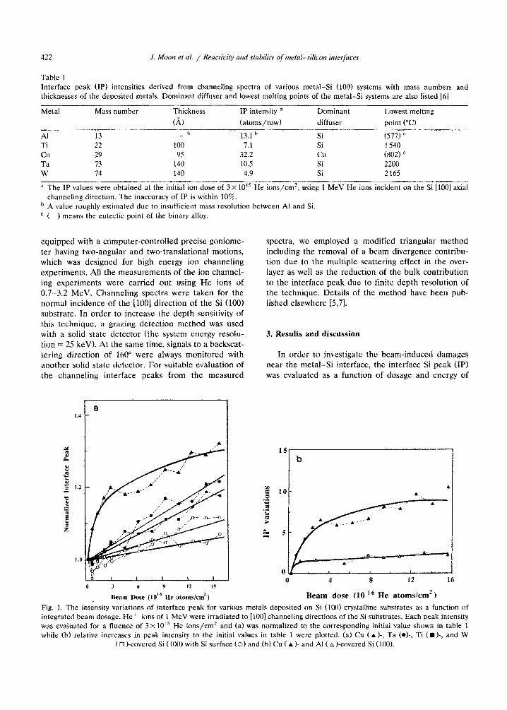
Fig. 1. The intensity variations of interface peak for various metals deposited on Si (100) crystalline substrates as a function of integrated beam dosage. He + ions of 1 MeV were irradiated to [it101 channeling directions of the Si substrates. Each peak intensity was evaluated for a fluence of 3 x IO’” He ions/cm’ and (a) was normalized to the corresponding initial value shown in table 1 while (b) relative increases in peak intensity to the initial values in table 1 were plotted. (a) Cu (A )-, Ta CO)-, Ti (a )-. and W
( q )-covered Si (100) with Si surface (0) and (b) Cu (A )- and Al (a )-covered Si (100).
J. Moon et al. / Reactivity and stability of metal-silicon interfaces 423
channeling He ions irradiated to metal-Si (100) speci- mens as well as the cleaned Si. The surface peak (SP) intensity for the cleaned Si 2 X 1 (1001 surface was found to be 4.0 atoms/row for l-MeV He ions, which was coincident with results of previous works per- formed under UHV conditions [4,8,9]. This means that the amounts of displaced surface Si atoms were almost the same for the clean reconstructed surface and the contaminated surface since a conventional vacuum chamber was used in the present ion scattering meas- urements. All the specimens examined below were covered with small amounts of contaminants such as 0 and C atoms, which were adsorbed during handling in air as well as partially during the measurements. How- ever, the amounts of contaminants are usually so small that the contamination negligibly affects the present analysis which deals only with atomic layers buried well below the specimen surface.
3.1. interface peak uariatio~s with beam dosuge
Metals deposited were catalogued into two groups: one consists of those forming stable sihcide layers, i.e., Ta, Ti, and W, and the other includes those forming unstable reaction layers, i.e., Cu and Al. Thicknesses of the deposited metals were listed in table 1 with the initial IP values measured at a fluence of 3 x 10” He ions/cm2. The difference in the initial IP values is a direct evidence that the interfa~ial reaction between metal and Si strongly depends on their combination. Roughly speaking, there may be a positive correlation between the interfacial reactivity and the lowest melt- ing points of possible silicides or the lowest eutectic points of possible alloys [6] as the present results shown in table 1. However, the number of exception is not small. On the other hand, the relation between the interfacial reactivity and the heats of formation was also discussed [6]. At present, the deduced conclusion is UnfortunateIy that there exist inherent reactivities at the interface between metal and Si which cannot sim- ply be related, with a reasonably small number of exceptions, to any conventional properties such as the melting points, the heats of formation, and so on.
Since beam-irradiation effects are expected to be approximately proportional to the amount of “visible” Si atoms exposed to the incident channehng He beam, IP values at various fluences were normalized to the initial values in table 1. Fig. 1 shows the no~alized IP variations with the integrated beam dose for the vari- ous metal-Si systems. In the cases of Ta-, Ti-, and W-Si, the IP variations are not very sensitive to the integrated beam dosage, compared with the case of Si with no deposited metal. The slopes of the normalized IP variations, or the normalized IP variations per unit dosage, AIP, are in approximate proportion to the integrated beam dose, and become steeper in the order
of Ta > Ti > W, as shown in fig. la. For the Ta- and W-Si systems, though the masses and thicknesses of the deposited metals are nearly the same, the Ta-Si system yields larger AIP than the W-Si system does. This demonstrates that the observed difference in AIP should be related not only to the collision process depending on the atomic masses, the nucleus charges and the numbers of deposited metal atoms, but also to the inherent reactivity difference between both metal- Si systems. The latter also determines the various ini- tial IP values as described above.
In the Cu and Al cases, the IP variations with beam dosage are rapid and large at the onset of the beam irradiation, and tend to saturate rapidly at high beam fluences, as shown in fig. lb. The beam-induced dam- age effect near the metal-Si interface is larger for the Cu-Si system than the Al-Si system. These IP varia- tions are similar to that of the Au case previously reported [lo]. The saturation phenomenon at high flu- ences suggests the short supply of the metal atoms to an unreacted region of the Si substrate through the reacted Si region. The mechanism of these initial be- haviors can be considered to be due to a kind of the beam-induced mixing effect [ll-131 between the de- posited metal CL&U) and substrate Si atoms, which will be discussed later.
The metal dependence of the IP variations with the integrated beam dose correlates well with that of the initial IP values (table 1). After the metal deposition on the Si crystal, the mixed layers are immediately formed in according to the inherent reaction character- istics between the metal and silicon atoms. These re- acted Si layers cannot retain the original c~stallinity any more, leading to an increase of the silicon IP intensity, which is the key to the present evaluation of the reactivity between the metal overlayer and silicon substrate.
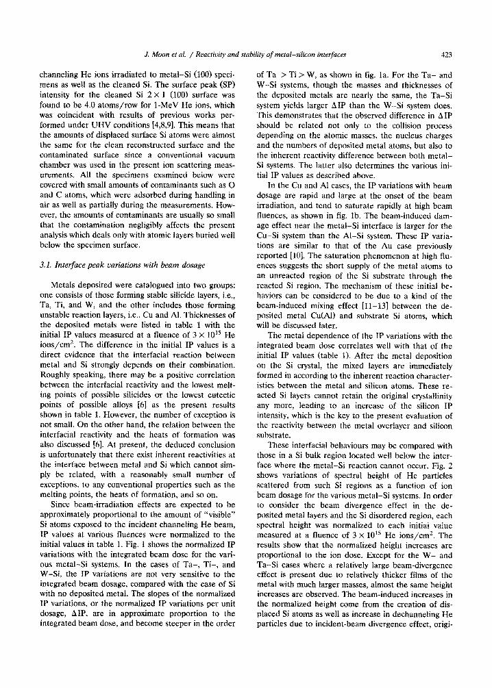
These interfacial behaviours may be compared with those in a Si bulk region located well below the inter- face where the metal-% reaction cannot occur. Fig. 2 shows variations of spectral height of He particles scattered from such Si regions as a function of ion beam dosage for the various metaLSi systems. In order to consider the beam divergence effect in the de- posited metal layers and the Si disordered region, each spectral height was normalized to each initial value measured at a fluence of 3 x 10¹⁵ He ions/cm2. The results show that the normalized height increases are proportional to the ion dose. Except for the W- and Ta-Si cases where a relatively large beam-divergence effect is present due to relatively thicker films of the metal with much larger masses, almost the same height increases are observed. The beam-induced increases in the normalized height come from the creation of dis- placed Si atoms as well as increase in dechanneling He particles due to incident-beam divergence effect, origi-
424 J. Moon et al. / React&y and stabiiity of metal-silicon interfaces
o.st 0 4 8 12 16
Beam Dose (10 I6 He atoms/cm2~ Fig. 2. Spectral height variations with integrated beam dosage for various metaLSi systems. During irradiation of 1 MeV He ions to Si (100) substrates, backscattered He particles from a Si region well below the metaLSi interface were counted. Each value was normalized to initial one measured at a dosage of 3 X 10j5 He ions/cm* for Cu ( A )-, Al ( A )-, Ta(*) -,
TX m I-, W( q l-covered Si and Si (01.
nating from the beam-induced displacements of crys- talline Si atoms. These behaviours are clearly different from the IP variations described above, especially in the Cu and Al cases. Thus, the beam-induced IP varia- tions should be related directly to the interfacial prop- erties.
3.2. Interface peak variations with incident beam energy
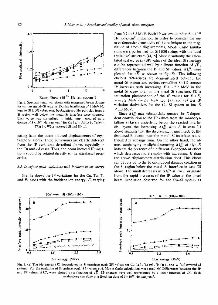
Fig. 3a shows the IP variations for the Cu, Ta, Ti, and W cases with the incident ion energy, E, varying
He’ -W Si (I#ll-<1@@>
P r 1 ii la .- I
Ion energy (MeV)
from 0.7 to 3.2 MeV. Each IP was evaluated at 6 x 10r5 He ions/cm2 influence. In order to consider the en- ergy-dependent sensitivity of the technique to the mag- nitude of atomic displacements, Monte Carlo simula- tions were performed for Si [loo] strings with the ideal (bulk-like) structure [14,151. Since resultantly the calcu- lated surface peak (SP) values of the ideal Si structure can be represented well by a linear function of @, differences between the IP and SP values, Al,?, were plotted for &? as shown in fig. 3b. The following obvious differences are demonstrated between the metaLSi system and perfect crystalline Si: (1) steeper IP increases with increasing E < _ 2.2 MeV in the metaLSi cases than in the ideal Si structure, (2) a saturation phenomenon of the IP values for E > I& = N 2.2 MeV (- 2.5 MeV for Ta), and (3) less IP
variation derivatives for the Cu-Si system at low E < 1.3 MeV.
Since AIF may substantially remove the E-depen- dent contribution to the IP values from the monocrys- talline Si layers underlying beiow the reacted interfa- cial layers, the increasing Al: with E in case (1) above suggests that the displacement magnitude of the displaced Si atoms near the metaLSi interface is dis- tributed in subangstroms. On the other hand, the al- most unchanging or slight decreasing AI&’ at high E indicate the presence of a different E-dependent effect which decreases more rapidly with increasing E than the above displacement-distribution does. This effect can be related to the beam-induced damage creation in the Si region below the metal-Si interface in case (2) above. The small decreases in AI$” at low E originate from the rapid increases of the IP value at the onset beam i~adiation observed for the Cu-Si system as
He’ Y Si (lOO)-<lOO> z I
& 20 I rJ.
z d b z 0
0.8 1.2 X.6
lion energy (MeV)
Fig. 3. (a) The He energy (El dependence of Si interface peak (IP) values for Cu (A I-, Ta (*)-, Ti (m)-, and W (fl)-covered Si systems. For the evalution of Si surface peak (SP) values CO). Monte Carlo calculations were used. (b) Differences between the IP and SP values, AI&‘, were plotted as a function of a. SP changes were well represented by a linear function of fi. Each
evaluations was done at a fixed ion dose of 6 x 10¹⁵ He ions/cm’.
J. Moon et al. / Reactivity and stability of metal-silicon interfaces 425
shown in fig. 1 (case (1) above). In other words, since the beam-induced effect per unit depth is larger for lower E, larger IP increases are observed for lower E at a given dosage (small enough for a substantial satu- ration in IP increase not to be observed). For the other metal-Si systems, the initial increases of IP values are sufficiently small that a significant dose effect does not appear explicitly in fig. 3 and that at the low energies below Es the E-dependent displacement-sensitivity of channeling He particles more effectively determines the energy-dependent IP variations for the displace- ment-distributed Si atoms.
3.3. Possible mechanism of beam-induced displacements
In order to describe the reaction between the metal and silicon, several models have been proposed. Among them, the atomic diffusion model by Tu [16] and the electronic screening model by Hiraki [17] can lead to clear predictions, which may be discussed using the present results described above. Both models obviously need considering the metal-dependent reactivity with Si, since the metal-dependent reactivity at the initial stage (table 1) cannot be explained without a consider- able difference in the inherent reactivity of Si with the various metals. The inherent reactivity also plays an important factor for the beam-induced reaction (figs. 1 and 3). We will now consider our beam-induced mixing data in relation to the above two models.
In the case of the beam-induced reaction, the fol- lowing two factors should additionally be taken into account. The first one is a beam-irradiation effect on the atomic diffusion of the deposited metals. A direct effect of the incident He ions is collision-induced diffu- sion of the metal atoms, or the knock-on effect of the high energy particles. This effect may not be a key factor since the different IP increases are observed between the Ta-Si and W-Si cases where the knock-on effect of the metal atoms are expected to be almost the same. On the other hand, an indirect effect is defect- induced diffusion of the metal atoms, which can take place through defects created in the Si substrate by the collision cascades. However, the collision-induced dif- fusion may not be very important in the present metal- Si systems since Si is the dominant diffuser in the Ti-, Ta-, and W-Si systems with except ion of the Cu-Si system which is not very well known as for the low temperature diffusion [18]. Thus, it is concluded that the beam-induced diffusion may play only a minor role only in the beam-induced reactions observed (except for the Cu-Si system), although a diffusion-induced reaction may occur as the diffusion model tells.
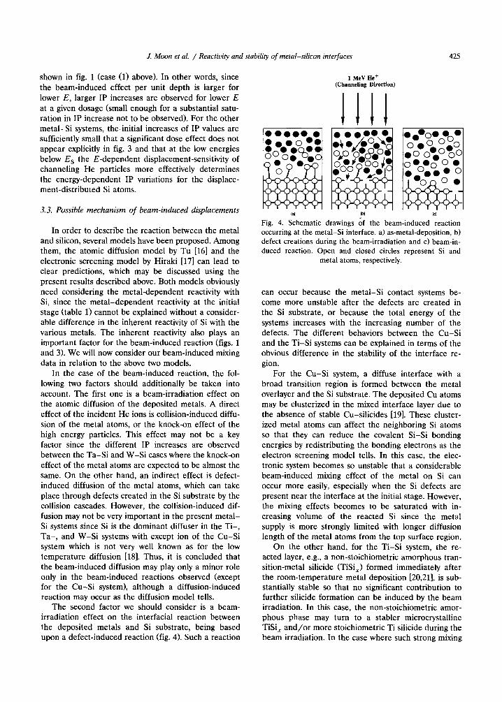
The second factor we should consider is a beam- irradiation effect on the interfacial reaction between the deposited metals and Si substrate, being based upon a defect-induced reaction (fig. 4). Such a reaction
1 MeV He+ (Channeling Direction)
,a) lb) cc,
Fig. 4. Schematic drawings of the beam-induced reaction occurring at the metal-Si interface. a) as-metal-deposition, b) defect creations during the beam-irradiation and c) beam-in- duced reaction. Open and closed circles represent Si and
metal atoms, respectively.
can occur because the metal-Si contact systems be- come more unstable after the defects are created in the Si substrate, or because the total energy of the systems increases with the increasing number of the defects. The different behaviors between the Cu-Si and the Ti-Si systems can be explained in terms of the obvious difference in the stability of the interface re- gion.
For the Cu-Si system, a diffuse interface with a broad transition region is formed between the metal overlayer and the Si substrate. The deposited Cu atoms may be clusterized in the mixed interface layer due to the absence of stable Cu-silicides [19]. These cluster- ized metal atoms can affect the neighboring Si atoms so that they can reduce the covalent Si-Si bonding energies by redistributing the bonding electrons as the electron screening model tells. In this case, the elec- tronic system becomes so unstable that a considerable beam-induced mixing effect of the metal on Si can occur more easily, especially when the Si defects are present near the interface at the initial stage. However, the mixing effects becomes to be saturated with in- creasing volume of the reacted Si since the metal supply is more strongly limited with longer diffusion length of the metal atoms from the top surface region.
On the other hand, for the Ti-Si system, the re- acted layer, e.g., a non-stoichiometric amorphous tran- sition-metal silicide (TiSi,) formed immediately after the room-temperature metal deposition [20,21], is sub- stantially stable so that no significant contribution to further silicide formation can be induced by the beam irradiation. In this case, the non-stoichiometric amor- phous phase may turn to a stabler microcrystalline TiSi, and/or more stoichiometric Ti silicide during the beam irradiation. In the case where such strong mixing

426 .I. Moon et al. / ~eactii~i~ and st~bi~~~ of petal-silicon interlaces
reactions as in the Cu-Si case are not induced by the high energy He beam, no saturation phenomena can be observed under the experimental conditions employed.
Computer simulations might help one to undcr- stand the beam-induced damages. As a matter of fact, an empirical simulation was carried out for beam-in- duced metal-Si interfacial reaction with very thin over- layers ( < 10ML) [lo], where self-diffusion of metal atoms is not very important. In the present case, the self-diffusion effect is more important. In any case, since the inherent reactivity at the interface depends on the metal-Si combination, it may be difficult to simulate the beam-induced interfacial phenomena when the chemical nature at the interface is not well known. Thus, a more quantitative model on the inter- facial reaction than the present model is required for meaningful simulations.
4. Conclusions
We have drawn the foliowing conclusions from the present beam irradiation experiments measuring the channeling interfacial Si peak (IP) for Cu-, Al-, Ta-, Ti-, and W-Si (100) systems by using high energy (_ MeV) He ions.
(1) For the Ta-, Ti- and W-Si systems, the IP increase (AIP) is not very sensitive to the beam dose, corresponding to the existence of the stable interfaces and silicides between the deposited metal and Si. In the order of Ta, Ti, and W, AIP observed become large.
(2) For the Cu- and Al-Si systems, AIP is large at the very initial beam-irradiation with subsequent satu- ration phenomena, corresponding to the absence of the stable interfaces and silicide. For the Cu case, AIP observed is the largest of the examined metal-Si sys- tems.
(3) The IP values increase with incident energy E of He ions more than the (E-dependent) surface peak intensity values of the ideal crystal for E < 2.2 MeV (2.5 MeV in the case of Ta-Si system); above this energy saturation of the IP increases with E is ob- served. This indicates that the displacement magnitude of the displaced Si atoms is distributed in sublngstriims. The beam-induced damage-creation effect is also in- cluded in the E-dependence of the IP values.
(4) The observed beam-induced phenomena can be explained in terms of (a) the inherent reactivity be- tween the metal and Si, (b) the colIision-induced diffu- sion of the metal atoms into the crystalline Si, and (c)
the defect-induced reaction in the near-interface crys- talline Si region. The contributions from (a) and (c) to the beam-induced interfacial reaction may be impor- tant in the present metal-Si systems.
Acknowledgements
This work was partly supported by a grant-in-aid for Scientific Research on Priority Areas of “Metal-Semi- conductor Interfaces” from the Minist~ of Education, Science and Culture of Japan.
References
[II
121
[31
141
1st
t61
[71 181
191 [lOI
[ill
[I21
1131
1141
[151 [I61 [171 [181
[191
DOI
IN
A. Hiraki. Surf. Sci. 168 (1986) 74; Appl. Surf. Sci. 56-58 (1992) 370. L.C. Feldman, P.J. Silverman and I. Stensgaard, Nucl. Instr. and Meth. 168 (1980) 589. E.J. Van Loenen, M. Iwami, R.M. Tromp and J.F. Van der Veen, Surf. Sci. 137 (1984) 1. T. Narusawa, K. Kinoshita, W.M. Gibson and A. Hiraki, Phys. Rev. B24 (198114835. 3. Moon, T. Ito and A. Hiraki, Appf. Surf. Sci. 56-58 (1992) 469. S.P. Muraka, in: Silicides for VLSI Applications, (Academic Press, New York, 1983). T. Ito, Jpn. J. Appl. Phys. 25 (1986) 902. G.A. Smith, Li Luo and W.M. Gibson, J. Vat. Sci. Technol. 8 (1990) 1427. T. Ito and W.M. Gibson, Jpn. J. Appl. Phys. 6 (1987) 841. T. Ito and W.M. Gibson; Nucl. Instr. and Meth. I312 (1985) 382. B.M. Paine and R.S. Averback, Nucl. Instr. and Meth. B7/8 (1985) 666. S.S. Lau, B.Y. Tsaur, M. van Allmen, J.W. Mayer, B. Stritzker, C.W. White and B. Appleton, Nucl. Instr. and Meth. 182/183 (1981) 97. J.W. Mayer, B.Y. Tsaur, S.S. Lau and L.S. Hung, Nuct. Instr. and Meth. 182/183 (1981) 1. K. Kinoshita, T. Narusawa and W.M. Gibson, Surf. Sci. 110 (1981) 369. T. Ito and W.M. Gibson, Surf. Sci. 161 (1985) 115. K.N. Tu, Appl. Phys. Lett. 27 (1975) 221. A. Hiraki, J. Electrochem. Sot. 127 (1980) 2662. Marc A. Taubenhlatt and C.R. Helms, J. Appl. Phys. 53 (1982) 6308. S.A. Chambers and J.H. Weaver, J. Vat. Sci. Technol. A3 (1985) 1929. S. Ogawa, T. Kouzaki, T. Yoshida and R. Sinclair, J. Appl. Phys. 70 (1991) 827. K. Holloway and R. Sinclair, J. Appl. Phys. 61 (1987) 1339.


![Spectral and scattering theory for space-cuto P models ...The spectral and scattering theory of Hwas studied in [DG] by adapting methods originally developped for N particle Schr odinger](https://img.dokumen.tips/doc/110x75/5f700e57068eb9037f6d18f4/spectral-and-scattering-theory-for-space-cuto-p-models-the-spectral-and-scattering.jpg)


![Spectral and Scattering Theory for Space-Cutoff ϕ Models ...c... · The spectral and scattering theory of H was studied in [2] by adapting meth-ods originally developed for N-particle](https://img.dokumen.tips/doc/110x75/5f700db082dc1c0e0a57dc62/spectral-and-scattering-theory-for-space-cutoi-models-c-the-spectral.jpg)