Embed Size (px)
Citation preview

ION
www.MaterialsViews.comwww.advenergymat.de
ve and and fea-
er ,
Rationally Designed, Three-Dimensional Carbon Nanotube
CO
MM
UN
ICAT
Devices designed to convert sunlight into usable sources of energy have become the focus of increased attention in the past
solution-phase condensation process, [ 9–11 ] conductichemically robust CNF scaffolds with tunable pitch
Cary L. Pint , Kuniharu Takei , Rehan Kapadia , Maxwell Zheng , Alexandra C. Ford , Junjun Zhang , Arash Jamshidi , Rizia Bardhan , Jeffrey J. Urban , Ming Wu , Joel W. Ag Michael M. Oye , and Ali Javey*
Back-Contacts for Effi cient Solar Devices
rces. [ 1 ] ture shape/size are obtained. To explore the utility of the pro-coated water
2 /CNF 2 , [ 18–23 ] orbing collec- of up e 3-D
red to ortant atings sem-
bit the lution. roach CNF
emical i cata-uctive CNF its an tween ocess,
decade due to the diminishing nature of fossil fuel resouAs a result, recent research efforts have focused on imprsolar device performance and cost using novel processes,rials and device technologies. [ 2 , 3 ] One example includes thof three-dimensional (3-D) architectures to enhance the ccollection effi ciency and photon management of the devicIn such a device concept, the effi ciency of thin fi lm solar dcan be enhanced by orthogonalizing the light absorptiocarrier collection processes, especially for the material sythat exhibit low minority carrier lifetimes. [ 7 ] In addition, srefl ectance is reduced and the absorption is enhancedimproving the overall conversion effi ciency. One route forcating 3-D solar devices involves the use of textured subsand/or back-contacts followed by the conformal depositthin fi lms of the absorber material. [ 8 ] In this regard, expscalable and tunable nanotexturing processes with high-ratio features is required.
Here, we demonstrate the fabrication of textured cnanofi ber (CNF) arrays for the back-contact of solar dwith improved photon capture properties. Using a sca
Dr. C. L. Pint , Dr. K. Takei , R. Kapadia , M. Zheng , A. C. Ford , J. Zha Prof. A. Javey Department of Electrical Engineering and Computer Science
© 2011 WILEY-VC1040 wileyonlinelibrary.com 40–1045
alable Here,
.6 cm 2 itions. verti-rently s with struc-ensity 5 μ m
rform-sulted r else struc-ghout
o coat 0 nm) light-wn in
University of California, BerkeleyCA 94720 USA, Material Sciences DivisionLawrence Berkeley National LaboratoryBerkeley, CA 94720 USAE-mail: [email protected] Dr. A. Jamshidi , Prof. M. Wu Department of Electrical Engineering and Computer ScienceUniversity of CaliforniaBerkeley, CA 94720 USA Dr. R. Bardhan , Dr. J. J. Urban The Molecular FoundryMaterial Sciences DivisionLawrence Berkeley National LaboratoryBerkeley, CA 94720 USA Dr. J. W. Ager Material Sciences DivisionLawrence Berkeley National LaboratoryBerkeley, CA 94720 USA Dr. M. M. Oye NASA Ames Research CenterMoffett Field, CA 94035, USA
DOI: 10.1002/aenm.201100436
H Verlag GmbH & Co. KGaA, Weinheim Adv. Energy Mater. 2011, 1, 10
oving mate-e use arrier es. [ 4–6 ] evices n and stems urface , thus fabri-trates
ion of loring aspect
arbon evices lable,
posed approach, the nanotextured CNF electrodes are with conformal thin fi lms of TiO 2 absorber layer for oxidation. [ 12–17 ] Unlike the use of other reported TiOarchitectures, or nanotubes and nanowires made of TiOthis morphology allows us to design antirefl ective abslayers to decouple and optimize absorption and carrier tion. Based upon this, we demonstrate an enhancementto 3 times in the short circuit current density ( J SC ) for thCNF/TiO 2 photoelectrochemical (PEC) device as compaits planar counterpart. Antirefl ection is particularly impas it is not feasible to use conventional antirefl ective coin PEC cells since the effective junction is formed at theiconductor-liquid interface. [ 24 ] Such a coating would inhiinjection of photo-generated minority carriers into the so
Figure 1 demonstrates the general fabrication appfor textured CNF back-contacts. First, vertically alignedarrays (Figure 1 a,c) are grown in a plasma-enhanced chvapor deposition system on Si/SiO 2 substrates using Nlyst thin fi lms (thickness, 30 nm), supported on condCu/Ti bilayers (thickness, 200/30 nm). [ 25 ] The fabricatedarray is electrically addressable by the substrate and exhibaverage vertical height of ∼ 10 μ m and CNF diameters be10-120 nm, as measured by SEM. Following the growth prthe vertically aligned CNF arrays are textured using a scsolution-phase condensation process (Figure 1 b,d). [ 9–11 ] CNFs are exposed to a 20 μ L drop of acetone ( ∼ 0.6 × 0sample size) which is then dried under ambient condUpon drying, capillary forces cause reorganization of thecally aligned carbon nanofi ber morphology, which is inhedependent on the surface tension of the liquid. [ 9 ] Solventdifferent surface tensions were found to yield variable tures upon drying, with acetone yielding the highest dof compact pillar structures with a base diameter of 4–(Figure 1 d) that resulted in the most optimal device peance. The use of other solvents and drying conditions rein either larger pillars with smaller out-of-plane angles oridge-like pillars that formed cellular, interconnected tures. Therefore, acetone condensation was utilized throuexperiments described here.
Atomic layer deposition (ALD) at 250 ° C was utilized tTiO 2 thin fi lms with varied thicknesses ( T TiO2 = 80–40on the surface of the texturized CNF templates as theabsorbing material. As demonstrated in SEM images sho
ng ,

1041C
CO
MM
UN
ICATIO
N
rary.com
www.MaterialsViews.comwww.advenergymat.de
since the generated carriers are mostly lost to recombination prior to reaching the surface.
the per-itecture, O 2 /CNF graphite lectrode ermody-ree-elec-y under Nernst ade by ite sur-
per and igure 3 c graphite f T TiO2 .
sistently as com-e same
t could contrib include (i) red optical
, and ctance
sessed. asured textur-. The
ultra-planar d light sured, urface e sub-f light ned as .2–1.3
tecture l anti-
use of articu-e 2–3x
[ 4 , 31–33 ] togen- inter-e car-to J SC
cesses. , [ 29 , 30 ]
can be harac-orbed) es that would F/TiO 2
Figure 2 a–d, this TiO 2 coating is highly conformal. The TiO 2 thicknesses were confi rmed for these structures by utilizing
a
t
l 1yehahefGnt
O
eno
w2r
n
Figure 1 . (a,b) Scheme of process depicting the capillary-force drying and texturizinas-grown carbon nanofi ber arrays, (c) SEM image of as-grown carbon nanofi ber a(d) SEM image of a texturized carbon nanofi ber array. Scale bar in (c) and (d) is 3 μ m
© 2011 WILEY-VAdv. Energy Mater. 2011, 1, 1040–1045
destructive SEM imaging (Figures 2 c,d) where the pillintentionally broken to expose the conformal TiO 2 lathe CNFs within. In order to determine the crystal sof the TiO 2 , x-ray diffraction (XRD) and Raman specmeasurements were performed as shown in Figures 2 erespectively. From the XRD spectrum, the peaks labe“A” correspond to those of an ordered anatase phase(body-centered cubic, I41/amd (141) JCPDS Card No. In addition, Raman spectroscopy depicts low frequencat ∼ 147, 401, 520, and 639 cm − 1 correlating well to thmodes of anatase TiO 2 , also independently verifying tence of anatase TiO 2 . [ 26 ] It should be noted that anathas a slightly higher band gap energy (3.2 eV) than ottalline phases of TiO 2 , but has also been suggested to beffective water oxidation photocatalyst. [ 27 ] Also, evident Raman spectrum are the broad and overlapping D and centered around 1380 and 1600 cm − 1 , respectively arisithe sp 3 hybridized graphitic structure of CNFs, similar walled nanotubes [ 28 ] (Figure 2 (d)).
Figure 3 b shows the current-potential curves for Tistructures with various T TiO2 utilizing an aqueous 1 Melectrolyte solution. The measurements were taken un1.5 G (1 sun) solar radiation using a three-electrodequipped with a Pt counter electrode and an Ag/AgCl relectrode. AM 1.5 G illumination was utilized as a stacompare the effect of electrode structure on the photgenerated by the TiO 2 absorber. As expected, the overaured photocurrent is found to increase with increasinness for T TiO2 < ∼ 300 nm due to enhanced absorption, greatest margin of increase in the thickness range of 80–This range corresponds to 1-3 times the previously minority carrier diffusion length in TiO 2 ( L D ∼ 70–100 nBeyond T TiO2 ∼ 300 nm (i.e., T TiO2 > ∼ 3 L D ), further incthe thickness does not result in photocurrent enha
In order to directly demonstrate formance benefi ts of 3-D device archwe compare the measured J SC of Tistructures to those of planar TiO 2 /devices. Here, J SC for the three-emeasurement is defi ned at the thnamic threshold voltage where the thtrode cell has a net gain of free energillumination (0.216 V) based on theequation. The planar devices were mthe ALD of TiO 2 on a pressed graphface polished with 900 grit sandpacleaned prior to coating. Shown in Fare the J SC values for both the planar and CNF templates as a function oThe 3-D TiO 2 /CNF architecture conexhibits 2-3x enhancement in J SC pared to the planar devices with thTiO 2 physical thickness.
We now consider factors thaute to the observed enhancement. These uced surface refl ectance, (ii) enhanced
ength for the same TiO 2 physical thickne
g of the rray, and .
H Verlag GmbH & Co. KGaA, Weinheim wileyonlinelib
path l ss(iii) improved carrier collection effi ciency. The refl eof planar and 3-D textured samples can be directly asShown in Figure 4 a is the percent refl ectivity, R , as mefor the planar TiO 2 /graphite substrate, and the coated ized CNF templates. For both samples, T TiO2 ∼ 60–80 nmrefl ectivity of the CNF templates is R 3-D = 0.5-0.7% in theviolet and visible regimes, whereas the refl ectivity of the graphite is R planar = 14–22%. Here, the effect of diffuseis ignored which can affect the absolute refl ectance meabut will not change the observed trend. The drastic low srefl ectance observed for 3D TiO 2 structures arises from thwavelength tip-diameter, minimizing the interaction owith the surface. An enhancement factor, γ , can be defi γ = (100- R 3-D )/(100- R planar ), which yields a suggested 1times increase in device performance for the 3-D archibased on minimized refl ections. Given that conventionarefl ective coating cannot be utilized in PEC devices, thea structural anti-refl ective approach explored here is plarly important. Yet, refl ectance alone does not explain thenhancement in J SC that is experimentally observed.
Next, we examine the effect of increased optical pathin textured CNF structures. The probability of a phoerated carrier to diffuse to the semiconductor-electrolyteface scales as P ∝ exp
(TTi O2
L D
) , suggesting that only th
riers generated within ∼ 3 L D of the surface contribute with the rest mostly being lost to recombination proFor TiO 2 , given the previously reported L D = 70–100 nmthe maximum active thickness within which the carrier collected is hence only ∼ 300nm. However, the optical cteristic length ( ∼ 90% of all above-gap photons are absis on the order of 1 μ m. [ 34 ] This suggests that structurdecouple the optical and carrier collection path lengthsresult in enhanced device effi ciencies. In this regard, CN
rs were yer and tructure roscopy and 2 f, ed with of TiO 2 08976). modes known e pres-
se TiO 2 er crys- a more rom the
bands g from
o multi-
2 /CNF NaOH der AM e setup ference dard to current
ll meas-g thick-
ith the 20 nm.
eported m). [ 29 , 30 ] rease in cement

CO
MM
UN
ICATI
ON
www.MaterialsViews.comwww.advenergymat.de
1045
architecture explored here presents an advantage. A scheme depicting this mechanism is shown in Figure 4 b. In this case, the high aspect-ratio structure inherent in the textured CNF
sso
hs
The average out-of-plane angle of the textured CNFs (1–2 μ m structure base radius, 10 μ m height) explored here is θ = 75 ° –85 ° on average based on SEM characterization (Figure S1). For
ons t in rial ath
ght. ably an
Figure 2 . (a,b) SEM images of texturized carbon nanofi ber arrays coated with (a) 80 nm TiO 2 , and (b) 400 nm TiO 2 . Inset in both images are higher magnifi cation views. (c,d) Top-view SEM image of a broken TiO 2 /CNF pillar with (c) 80 nm and (d) 400 nm TiO 2 coating. Characterization of TiO 2 /CNF architectures using (e) XRD and (f) Raman spectroscopy to confi rm the presence of anatase TiO 2 and the wall quality of the CNFs, respectively.
1042 © 2011 WILEY-VCwileyonlinelibrary.com
electrodes results in the formation of a semiconductor abwith a normal vector (along the direction of the thickneented with some angle > 60 ° relative to the average angle dent radiation. This means that the effective thickness semiconductor is signifi cantly greater than the actual pthickness meaning that many more photons will be abcloser to a point where they can be collected.
H Verlag GmbH & Co. KGaA, Weinheim Adv. Energy Mater. 2011, 1, 1040–
orber s) ori-f inci-of the ysical orbed
ideal normal incident radiation, geometrical consideratisuggest a structure with θ ∼ 80 ° to yield ∼ 6x enhancementhe optical path length as compared to the physical matethickness. This means for T TiO2 = 300 nm ∼ 3 L D , an optical plength of ∼ 1.8 μ m can be achieved for the normal incident liIn actuality, this simple geometric consideration consideroverestimates the enhancement factor since it assumes only

1043© 2011 WILEY-V
CO
MM
UN
ICATIO
N
rary.com
www.MaterialsViews.comwww.advenergymat.de
Adv. Energy Mater. 2011, 1, 1040–1045
ideal normal irradiation. Therefore, it should be used simply as a guideline rather than a strict calculation.
c anal-re S3), fi cantly only a to fl at physics these ture is e from hat the micon-taining r maxi-ld ide- yields
nergies nclude ddition . band
Figure 3 . (a) Scheme depicting the three-electrode setup utilideposited on conductive CNF back contacts as the absorb1.5 G solar irradiation, and the reference (AgCl/Ag) and counte(Pt) confi guration. (b) Current-potential curves of TiO 2 coatenanofi ber arrays with different TiO 2 thicknesses using a simu1.5 G solar spectrum in 1 M NaOH (dark current: 150 nm Tand (c) Short circuit current density ( J SC ), defi ned at E = 0.216 Vthe three-electrode confi guration, as a function of TiO 2 thicknesTiO 2 coated, texturized CNFs and TiO 2 coated planar graphite.
Figure 4 . (a) Percent refl ectance as a function of wavelength for both planar graphite and coated, texturized CNF arrays demonstrating the anti-refl ective nature of the CNF arrays (60 and 80 nm TiO 2 coating, respectively). (b) Scheme depicting antirefl ective nature of highly 3-D structure, and visually demonstrating other possible means by which a 3-D structure can enhance behavior of a solar device.
CH Verlag GmbH & Co. KGaA, Weinheim wileyonlinelib
Experimental results in support of this geometriysis are discussed in the supporting information (Figuwhere similarly antirefl ective TiO 2 /CNFs with a signilower pillar density (and lower out-of-plane angle) yield2x enhancement to device performance in comparisonTiO 2 /graphite. Although this does not decouple the of the absorption and collection processes that lead toenhancements, it does demonstrate that electrode struca principle component of enhanced device performanc3-D semiconductor scaffolds. Therefore, this suggests ttextured CNF electrodes as a back-contact for a thin seducting absorbing layer offers a rational approach for obdevices with a balance between the effective thickness fomized absorption, and the actual thickness, which coually be tuned to L D . In this particular case of TiO 2 , thishigh effi ciency since most absorbed photons have enear the semiconductor band-gap energy. We further cothat rational design of semiconductor architecture, in ato chemical features of the semiconductor material (i.e
zing TiO 2 er of AM relectrode d carbon lated AM iO 2 /CNF) based on s for both

ION
www.MaterialsViews.comwww.advenergymat.de
Acknowledgements This work was partially funded by Berkeley Sensor and Actuator Center,
rk was oratory in the ported iences, ent of
dges a ogram
, 2011 , 2011, 2011
gap) are important in designing effi cient solar devices. This is particularly true for metal-oxides, where poor minority car-rier lifetimes can be compensated by tuning the structu
ei
ir
e
n
T
,
pt
e
t
a
729 . Chueh , K. Yu ,
. Takei ,
. Javey ,
A. Liu , S. Lee ,
16 . Wang ,
W. Lu ,
W. Lu ,
, 2036 . biology
tal Sci-
emistry
rnal of
rimes ,
. Mor , mes , J.
08 , 92 ,
mes , J.
. 2002 ,
Chueh ,
CO
MM
UN
ICAT
the electrode–perhaps yielding a route toward high effi devices from cheap and readily available materials.
In summary, we develop here a technique to fabricatable, 3D back-contact architectures for solar devices uta solution-textured CNF array template. Utilizing TiO 2 example absorber layer for PEC, a ∼ 3x enhancement of ured J SC was observed compared to planar substrateexplain the enhancement as being due to a combinatreduced refl ectance, enhanced absorption due to inceffective optical path length, and enhanced carrier colleffi ciency. The CNF back-contacts reported here presgeneric route for enhancing the performance of conventhin-fi lm solar devices, including PVs, especially for mawith small L D , less than the characteristic absorption lGraphitic CNFs are particularly attractive for such back-capplications due to their high conductance, lack of snative oxide layers, and high chemical robustness.
Experimental Section Aligned Carbon Nanofi ber Growth : Vertically aligned carbon na
(CNF) arrays were grown in a plasma-enhanced chemicaldeposition system utilizing C 2 H 2 , H 2 , and NH 3 precursors ugeneral approach described in more detail elsewhere. [ 25 ] The assamples had CNF vertical heights of ∼ 10 μ m based on SEM imCatalyst growth substrates were deposited utilizing electroevaporation using a 200 nm thick Cu layer, a 30 nm thick Ti laya 30 nm thick Ni layer on a p -Si substrate with 50 nm SiO 2 . The acts as an interdiffusion barrier for the Ni catalyst while still allowsubstrate to remain conductive following growth. Following growCNFs were exposed to liquid treatment using a drop of solventand then coated using ALD.
Atomic Layer Deposition : ALD coating was performed uPicosun Sunale system with intermittent 0.1 sec pulses of titetrakis isopropoxide and water vapor between 5 second N 2 The deposition temperature was 250 ° C. This condition resuldeposition rate of ∼ 0.2–0.3 Å/cycle.
AM 1.5 G Photocurrent Measurements : Photocurrent measurwere performed utilizing a Newport solar simulator (50–500 W,67005), which was tuned to 100 mW/cm 2 using a broadbandmeter. The photocell in which measurements were performecustom-made (Adams & Chittenden) with a 40 mm quartz wfor sample illumination. Prior to fi lling the photocell with 1 M electrolyte, the incident light intensity was calibrated to 1 sunexact position where the TiO 2 absorbing material is illuminacompare the effect of electrode structure or TiO 2 thickness on mephotocurrents, current-potential curves are taken for different sin the same confi guration. To prepare electrodes for measureAg paint is utilized to contact the Cu layer on which the 3-D nanofi bers are grown, and Dow Corning 3140 RTV waterproof adis utilized to isolate all surfaces of the sample except the activcoated CNFs.
Supporting Information Supporting Information is available from the Wiley Online Libfrom the author.
1044 © 2011 WILEY-VCwileyonlinelibrary.com
and Mohr Davidow Ventures. The synthesis part of this wosupported by a LDRD from Lawrence Berkeley National Lab(LBNL). Refl ectance measurements were performed using facilitiesElectronic Materials Program, LBNL, which is supported by supby the Director, Offi ce of Science, Offi ce of Basic Energy ScMaterials Sciences and Engineering Division, of the U.S. DepartmEnergy under Contract No. DE-AC02-05CH11231. A.J. acknowleSloan Fellowship and support from the World Class University prat Sunchon National University.
Received: July 31 Revised: September 28
Published online: October 26
re of ciency
scal-lizing as an meas-s. We on of eased ection ent a tional terials ngth.
ontact urface
nofi ber vapor
sing a -grown aging. -beam
er, and i layer
ing the th, the dried,
sing a tanium urges. s in a
ments model power d was indow NaOH at the ed. To asured mples
ments, carbon hesive e TiO 2
rary or
[ 1 ] N. S. Lewis , D. G. Nocera , Proc. Natl. Acad. Sci. 2006 , 103 , 15 [ 2 ] Z. Y. Fan , H. Razavi , J. W. Do , A. Moriwaki , O. Ergen , Y. L.
P. W. Leu , J. C. Ho , T. Takahashi , L. A. Reichertz , S. Neale , M. Wu , J. W. Ager , A. Javey , Nat. Mater. 2009 , 8 , 648 .
[ 3 ] P. V. Kamat , J. Phys. Chem. C 2007 , 111 , 2834 . [ 4 ] H. A. Atwater , A. Polman , Nat. Mater. 2010 , 9 , 205 . [ 5 ] Z. Y. Fan , R. Kapadia , P. W. Leu , X. B. Zhang , Y. L. Chueh , K
K. Yu , A. Jamshidi , A. A. Rathore , D. J. Ruebusch , M. Wu , A Nano Lett. 2010 , 10 , 3823 .
[ 6 ] Y. F. Huang , S. Chattopadhyay , Y. J. Jen , C. Y. Peng , T. Y. K. Hsu , C. L. Pan , H. C. Lo , C. H. Hsu , Y. H. Chang , C. K. H. Chen , L. C. Chen , Nat. Nanotechnol. 2007 , 2 , 770 .
[ 7 ] R. Kapadia , Z. Y. Fan , A. Javey , Appl. Phys. Lett. 2010 , 96 , 1031 [ 8 ] Y. J. Lin , G. B. Yuan , R. Liu , S. Zhou , S. W. Sheehan , D. W.
Chem, Phys. Lett. 2011 , 507 , 209 . [ 9 ] M. De Volder , S. H. Tawfi ck , S. J. Park , D. Copic , Z. Z. Zhao ,
A. J. Hart , Adv. Mater. 2010 , 22 , 4384 . [ 10 ] S. Tawfi ck , M. De Volder , A. J. Hart , Langmuir 2011 , 27 , 6389 . [ 11 ] Z. Z. Zhao , S. H. Tawfi ck , S. J. Park , M. De Volder , A. J. Hart ,
Physical Review E 2010 , 82 , 041605 . [ 12 ] D. Eder , A. H. Windle , Advanced Materials 2008 , 20 , 1787 . [ 13 ] D. Eder , A. H. Windle , Journal of Materials Chemistry 2008 , 18 [ 14 ] G. J. Wang , M. W. Lee , Y. H. Chen , Photochemistry and Photo
2008 , 84 , 1493 . [ 15 ] Y. Yao , G. Li , S. Ciston , R. M. Lueptow , K. A. Gray , Environmen
ence & Technology 2008 , 42 , 4952 . [ 16 ] H. T. Yu , X. Quan , S. Chen , H. M. Zhao , Journal of Physical Ch
C 2007 , 111 , 1 2987 . [ 17 ] H. T. Yu , X. Quan , S. Chen , H. M. Zhao , Y. B. Zhang , Jou
Photo chemistry and Photobiology a-Chemistry 2008 , 200 , 301 . [ 18 ] J. H. Bang , P. V. Kamat , Adv. Funct. Mater. 2010 , 20 , 1970 . [ 19 ] M. Z. Liu , N. D. Snapp , H. Park , Chem. Sci. 2011 , 2 , 80 . [ 20 ] G. K. Mor , K. Shankar , M. Paulose , O. K. Varghese , C. A. G
Nano Lett. 2005 , 5 , 191 . [ 21 ] K. Shankar , J. I. Basham , N. K. Allam , O. K. Varghese , G. K
X. J. Feng , M. Paulose , J. A. Seabold , K. S. Choi , C. A. GriPhys. Chem. C 2009 , 113 , 6327 .
[ 22 ] O. K. Varghese , C. A. Grimes , Sol. Energ. Mater. Sol. Cells 20 374 .
[ 23 ] O. K. Varghese , M. Paulose , K. Shankar , G. K. Mor , C. A. GriNanosci. Nanotechnol. 2005 , 5 , 1158 .
[ 24 ] T. Bak , J. Nowotny , M. Rekas , C. C. Sorrell , Int. J. Hyd. Energ 27 , 991 .
[ 25 ] H. Ko , Z. X. Zhang , J. C. Ho , K. Takei , R. Kapadia , Y. L. W. Z. Cao , B. A. Cruden , A. Javey , Small 2010 , 6 , 22 .
H Verlag GmbH & Co. KGaA, Weinheim Adv. Energy Mater. 2011, 1, 1040–1045

CO
MM
UN
ICATIO
N
www.MaterialsViews.comwww.advenergymat.de
[ 26 ] L. Miao , S. Tanemura , S. Toh , K. Kaneko , M. Tanemura , J. Cryst. Growth 2004 , 264 , 246 .
[ 31 ] K. R. Catchpole , A. Polman , Appl. Phys. Lett. 2008 , 93 , 191113 .
u , Appl.
pl. Phys.
[ 27 ] A. L. Linsebigler , G. Q. Lu , J. T. Yates , Chem. Rev. 1995 , 95 [ 28 ] M. S. Dresselhaus , P. C. Eklund , Advances in Physics 2000 , [ 29 ] P. Salvador , J. Appl. Phys. 1984 , 55 , 2977 . [ 30 ] M. Takahashi , K. Tsukigi , T. Uchino , T. Yoko , Thin Solid Fi
388 , 231 .
© 2011 WILEY-VAdv. Energy Mater. 2011, 1, 1040–1045
, 735 . 49 , 705 .
lms 2001 ,
[ 32 ] J. Y. Lee , P. Peumans , Optics Express 2010 , 18 , 10078 . [ 33 ] P. Matheu , S. H. Lim , D. Derkacs , C. McPheeters , E. T. Y
Phys. Lett. 2008 , 93 , 113108 . [ 34 ] H. Tang , K. Prasad , R. Sanjines , P. E. Schmid , F. Levy , J. Ap
1994 , 75 , 2042 .
1045CH Verlag GmbH & Co. KGaA, Weinheim wileyonlinelibrary.com

Copyright WILEY‐VCH Verlag GmbH & Co. KGaA, 69469 Weinheim, Germany, 2011.
Supporting Information for Adv. Energy Mater., DOI: 10.1002/aenm.201100436 Rationally Designed, Three-Dimensional Carbon Nanotube Back-Contacts for Effi cient Solar Devices Cary L. Pint, Kuniharu Takei, Rehan Kapadia, Maxwell Zheng, Alexandra C. Ford, Junjun Zhang, Arash Jamshidi, Rizia Bardhan, Jeffrey J. Urban, Ming Wu, Joel W. Ager, Michael M. Oye, and Ali Javey*

Submitted to
1
Copyright WILEY-VCH Verlag GmbH & Co. KGaA, 69469 Weinheim, Germany, 2010.
Supporting Information for Adv. Energy Mater., DOI: 10.1002/aenm.((please add manuscript number)) Rationally designed three-dimensional carbon nanotube back contacts for efficient solar devices Cary L. Pint, Kuniharu Takei, Rehan Kapadia, Maxwell Zheng, Alexandra C. Ford, Junjun Zhang, Arash Jamshidi, Rizia Bardhan, Jeffrey J. Urban, Ming Wu, Michael M. Oye, and Ali Javey*
Figure S1. Zoomed-in SEM image showing textured CNF pillars following acetone
condensation. In this case, the base of the pillar has a radius of ~ 1.4 µm with ϴ ~ 81°. It
should be noted that this undershoots the pillar height due to out-of-plane parallax during
imaging. On average, most pillars are found to have widths at the base of structure near or
below 2 µm, which validates the estimation of 75° < ϴ < 85° in the main text.

Submitted to
2
Figure S2. Simple geometrical argument relating the effective thickness of a semiconductor
coated on a three-dimensional nanostructure (teff) to the actual coated thickness (t) as a
function of the tilt angle of the nanostructure. In correspondence with Figure 4, the effect of a
three-dimensional structure can be envisioned to be most apparent when the tilt angle is
between 60°-85°, yielding a ratio of teff/t > 2. For light incident or nearly incident on the
semiconductor, this yields a significantly enhanced effective optical path length that can yield
enhanced absorption near the charge collection point. Such an effect is analogous, but yet
more tailorable, than the enhancement that occurs due to surface-bound scattering
nanoparticles.
Submitted to
3
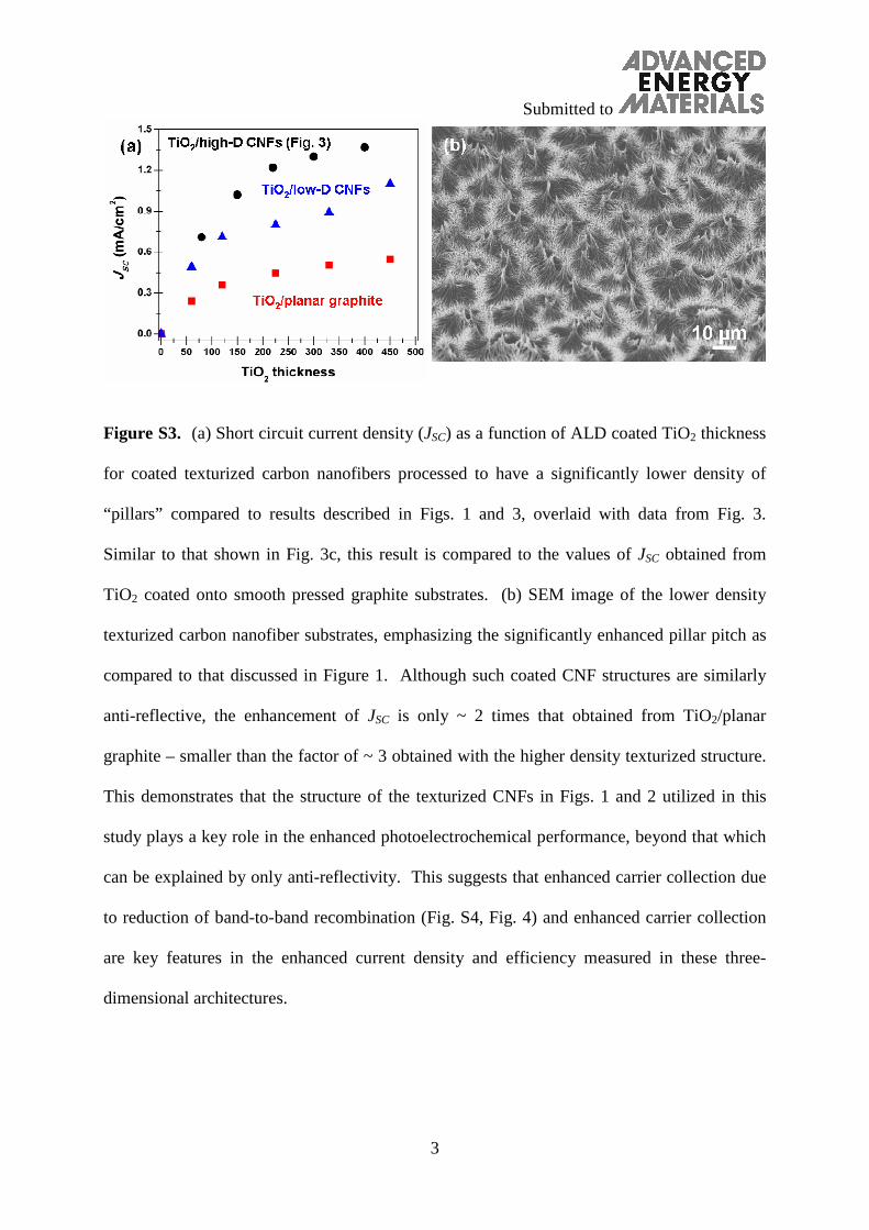
Figure S3. (a) Short circuit current density (JSC) as a function of ALD coated TiO2 thickness
for coated texturized carbon nanofibers processed to have a significantly lower density of
“pillars” compared to results described in Figs. 1 and 3, overlaid with data from Fig. 3.
Similar to that shown in Fig. 3c, this result is compared to the values of JSC obtained from
TiO2 coated onto smooth pressed graphite substrates. (b) SEM image of the lower density
texturized carbon nanofiber substrates, emphasizing the significantly enhanced pillar pitch as
compared to that discussed in Figure 1. Although such coated CNF structures are similarly
anti-reflective, the enhancement of JSC is only ~ 2 times that obtained from TiO2/planar
graphite – smaller than the factor of ~ 3 obtained with the higher density texturized structure.
This demonstrates that the structure of the texturized CNFs in Figs. 1 and 2 utilized in this
study plays a key role in the enhanced photoelectrochemical performance, beyond that which
can be explained by only anti-reflectivity. This suggests that enhanced carrier collection due
to reduction of band-to-band recombination (Fig. S4, Fig. 4) and enhanced carrier collection
are key features in the enhanced current density and efficiency measured in these three-
dimensional architectures.