Embed Size (px)
Citation preview

RAT5 Information Manual 1.2.1 October 2011
This manual is the complete reference document for RAT5, containing all aspects of
construction and operation.
This manual refers to RAT5 hardware version 1.2
Please check you are reading the latest version of this document by checking www.s9plus.com for any updates.
Please read this document fully before commencing construction
There are bound to be errors – please report any you find !
© GW4GTE 2011 www.s9plus.com

RAT5 Manual version 1.2.1
RAT5 Information Manual version 1.2.1 © GW4GTE 2011 Page 2 of 29
RAT 5
A Single-Conversion AM Receiver Kit for 160m or 80m
RAT5 kit of parts
Easy to Build This kit is suitable for constructors with little or no previous experience of kit-building. A basic level of soldering ability is however required. All components
are through-hole mounted i.e. no surface mount parts.

RAT5 Manual version 1.2.1
RAT5 Information Manual version 1.2.1 © GW4GTE 2011 Page 3 of 29
Contents
1 Introduction))))))))))))..))).).)).. 4 1.1 Modification Record - updates and corrections
2 Circuit Description))))))))).))))...)). 7 2.1 Key Features 2.2 RF / IF Circuits
2.2.1 RF Filter 2.2.2 Local Oscillator 2.2.3 IF Filter
2.3 AF and Squelch circuits 2.3.1 Squelch 2.3.2 Audio Filtering 2.3.3. Audio Amplifier
3 Construction).))))))))))))))..))) 10
4 Testing and Alignment )))))))))))))) 13 4.1 Power-off Tests 4.2 Power-on Tests
4.3 Local Oscillator alignment 4.4 IF and RF Alignment
4.4.1 IF Alignment
5 Interfacing ))))))))))))))))).)).. 18 5.1 Connection Method 5.2 Connections
5.3 Connecting an S-Meter 5.3.1 Calibration
5.4 Operation with a transmitter 5.5 Squelch Out 5.6 Power Sources 5.7 Choice of enclosure and Dimensions
6 Troubleshooting)))))))))..))))).)).. 22
6.1 Continuity checks 6.2 Voltage checks
7 Appendices))))))))))))))))).)).. 23 7.1 Parts List 7.2 Circuit diagrams - larger version 7.3 PCB Layout 7.4 “Anti-SSB” AGC modification for nuisance-free monitoring 7.5 Builder’s Gallery

RAT5 Manual version 1.2.1
RAT5 Information Manual version 1.2.1 © GW4GTE 2011 Page 4 of 29
1. Introduction What is it? The RAT5 is a single conversion AM receiver for 80m and 160m (operation on other frequencies is also possible). The receiver is based on the TDA1072A AM receiver IC which although obsolete is still available in quantity from at least one source and a reasonable number has already been obtained for kit builders. The low cost and ease of construction make this an ideal club project, and to this end component values are also provided to cover the Medium Wave where signals to tune into are plentiful. No previous experience of kit-building is required, just basic soldering skills. What does RAT5/FAT5 mean? For some years now the author has been playing about with home brew solid state AM transmitters, largely based on solid-state Class-E designs using low cost FETs. This is the so-called FAT5 series. The FAT5 name came from the original idea of making a solid state version of the AT5, using FETs. So, FET-AT5 became truncated to FAT5. RAT5 is an AM receiver to go with the FAT5 transmitter project. Maybe the complete RX/TX could be the FAT-RAT project? Is there a kit? Yes. Based around a 3”x2” drilled and tinned single-sided fibre-glass PCB the kit contains all the components for the project. All that is required in addition is an antenna, power source, loudspeaker, control knobs and case. For ordering details check www.s9plus.com or email the culprits below. It’s a big manual for a little kit? This is the complete reference document containing everything about RAT5. To just build the kit most of the sections can be ignored. Please read the entire document before starting construction. Project Support This is a supported project, with free advice offered before, during and after construction. Who to Blame Circuit design and PCB layout by Dave GW4GTE. PCB production and kit distribution by Eric GW8LJJ. Contact Points Dave GW4GTE: gw4gte @s9plus.com; address is QTHR or see QRZ.com Eric GW8LJJ: [email protected] ; address is QTHR or see QRZ.com Acknowledgements The author extends grateful thanks to ‘Ferric’ Eric GW8LJJ for the production of such excellent PCBs at ham-friendly prices. It is no exaggeration to say this and several other designs would never have seen the light of day as completed projects without Eric’s enthusiasm and support.

RAT5 Manual version 1.2.1
RAT5 Information Manual version 1.2.1 © GW4GTE 2011 Page 5 of 29
1.1 Modification Record Changes from the previous information manual
This manual is version 1.2.1. The previous manual was version 1.2.0
• Revised external squelch LED driver circuit figure 5.3
Changes to the PCB
The PCB to which this manual refers is version 1.2. The previous PCB was version 1.1.
New IF filter PCB Version 1.2 incorporates a different 455kHz filter. We have now managed to source a slightly narrower filter while keeping the kit price the same. The new filter is +/- 4.5 Khz wide at -6dB, previously it was +/- 6kHz wide at -6dB. The filter pinout is slightly different, requiring a modification to the PCB layout. If existing kit owners wish to try the new filter and are happy to adapt the previous PCB the new filter can be supplied as an upgrade. No other circuit changes are required. Track modification The PCB track around the pins of RV1, RV2 and RV3 have been thickened to provide more strength when using the potentiometer fixing threads to support the PCB.

RAT5 Manual version 1.2.1
RAT5 Information Manual version 1.2.1 © GW4GTE 2011 Page 6 of 29
2. Circuit Description Abbreviations: LO – Local Oscillator, CW – clockwise, CCW – Counter-clockwise PD – Potential difference, MW – Medium Wave, RF – Radio Frequency IF – Intermediate Frequency, IC – Integrated circuit, AM – Amplitude Modulation
AF – Audio Frequency, AGC – Automatic Gain control, RX – Receive(r) RAT5 is a varicap tuned single conversion superhet of conventional design based around the TDA1072A AM receiver IC. Figures 2.2 (RF/IF) and 2.5 (AF/Squelch) show the circuit in its entirety.
2.1 Key features High sensitivity Signals around 1uV PD are detectable. Good AM selectivity A 6-pole 455kHz AM filter has been selected for good adjacent channel selectivity. Bandwidth is +/-4.5 kHz at -6dB and +/-10kHz at -50dB. (previous version used a 6kHz filter). Input bandpass filter A two stage bandpass filter provides adequate protection against image breakthrough. Carrier Squelch The TDA1072A does not provide a squelch facility as it is intended for broadcast AM reception in consumer equipment. In amateur use a squelch feature is useful and this has been designed into the circuit. Low power consumption RAT5 consumes typically less than 50mA from a 9V to 15V supply making it suitable for battery operation.
2.2 RF/IF circuits Refer to Figure 2.1 The only active component in the RF/IF section apart from regulator VR1 is U1, a TDA1072A AM receiver IC around which everything else based. U1 performs all the main functions of a single conversion AM superhet including RF amplifier, LO, mixer, detector, AF pre-amp and AGC system, considerably simplifying the supporting circuitry. 2.2.1 RF Filter
With a 455kHz IF the image frequency is 910kHz away from the wanted signal. T1 and T2 together with C1 C2 and C3 form a two section bandpass filter with sufficient selectivity to prevent image breakthrough. Toko KANK3333 RF transformers are used for T1 and T2 as well as for L1 and L2. These are no longer manufactured by Toko, but equivalent transformers have recently become available in quantity. For simplicity the bandpass filter is fixed tuned. The added complication and expense of tracking varicap tuning is unnecessary for the narrow range of frequencies the intended application covers i.e. AM frequencies on 80m/160m

RAT5 Manual version 1.2.1
RAT5 Information Manual version 1.2.1 © GW4GTE 2011 Page 7 of 29
Figure 2.1 RF and IF circuit
A low-side LO on 80m and a high-side LO on 160m places the image in relatively quiet parts of the spectrum. The image frequency for 3615kHz is 2705kHz and the image frequency for 1963kHz is 2873kHz. Compare with say a low-side LO on 160m which would produce an image frequency in the MW broadcast band! Figure 2.2 below is an actual plot of the bandpass filter on 80m showing the image attenuation for a receive frequency of 3615kHz
Figure 2.2 Actual plot of RF bandpass filter on 80m

RAT5 Manual version 1.2.1
RAT5 Information Manual version 1.2.1 © GW4GTE 2011 Page 8 of 29
2.2.2 Local Oscillator (LO)
The LO frequency is determined by L1 C14 and the series combination of VC1 and varicap diode D1. VR1 provides a stabilised 5 V for tuning control RV1. VC1 can be varied to control the tuning range provided by RV1. R17 limits the minimum tuning voltage to around 0.9 V reducing the non-linearity at that end of the varicap’s tuning characteristic.
The circuit values given are for a low-side LO on 80m and a high-side LO on 160m. e.g. 3615kHZ RX, LO = 3160kHz ; 1963kHz RX, LO = 2418kHz For Medium Wave operation it is suggested the LO runs on the high side. The IC provides a buffered local oscillator output, and this is brought out to PL2 for use with a frequency display (future add-on project) and to assist with setting up.
2.2.3 IF Filter
The IF tuned circuit L2/C4 is tuned to 455kHz giving a good match into the IF filter FL1, a 6-pole ladder filter from Toko. This is a simpler solution than the circuit suggestions in the IC manufacturer’s data sheet. Figure 2.3 below shows an actual plot of the IF passband. (Note the graph shows passband response only, not ultimate out-of-band rejection for which a larger test signal would be required).
Figure 2.3 Actual plot of IF passband response of 6kHz filter (4.5kHz filter now supplied – response similar but narrower).
C9 and C10 give time constants for the internal AGC circuitry in line with data sheet recommendations. The AGC has a fast response which copes well with rapid signal fading. The S-meter output is brought out to PL4 for use with a meter or other display (see Section 5.3). The same line feeds the squelch circuitry shown in Figure 2.4.

RAT5 Manual version 1.2.1
RAT5 Information Manual version 1.2.1 © GW4GTE 2011 Page 9 of 29
2.3 AF and Squelch circuits Refer to Figure 2.4 2.3.1 Squelch
U2/a is one half of an LM358 op-amp IC, wired as a comparator. The LM358 was chosen for its ability to function at near-ground input levels while working off a single rail supply. RV2 sets the voltage on the non-inverting pin. AGC volts are fed into the inverting pin. With no input signal RV2 is adjusted such that pin 3 is more positive than pin 2. The output on pin 1 is high, saturating Q1 via D2 and R10. Q1, working as a potential divider with the U1 demodulated audio output impedance of 3k5 (as stated in datasheet) attenuates the ongoing signal to inaudible levels. When a carrier is received such that the AGC line at U2 pin 2 goes more positive than the level on pin 3 the comparator output will drop to zero, cutting off Q1 and enabling the audio path. The time constant provided by C30 / R10 reduces squelch clicks, as does the use of C20 to isolate Q1 from the bias chain R11/R12. External override muting is provided via limiting resistor R8. U2 is isolated by D2. Apply a positive voltage of 5V to 12V to PL3/6 to mute the receiver. This is intended for transceiver use as a means of muting the receiver while keeping the local oscillator running. C20 prevents squelch operation affecting the bias on U2/b, giving a clean squelch function with no clicks or thumps.
Figure 2.4 Audio and Squelch circuit
PL3/6 can also be used as an output to drive a squelch LED (see Section 5.5). PL3/6 is high on mute and low when the squelch is open.

RAT5 Manual version 1.2.1
RAT5 Information Manual version 1.2.1 © GW4GTE 2011 Page 10 of 29
2.3.2 Audio Filtering
The basic filtering suggested in the manufacturer’s data sheet has been discarded in favour of the circuitry shown. U2/b is an active low-pass filter with values chosen for the required response. R16 / C26 also add another pole of filtering. The aim was to produce a broadly level response from 300Hz to 3000Hz with a gentle roll-off at LF, steeper roll-off at HF, and a slightly rising response through the passband to improve clarity. Figure 2.5 below shows an actual frequency response plot of a prototype unit. The steepening LF roll-off is caused by the increasing reactance of C27 which becomes significant at lower frequencies.
2.3.3 Audio Amplifier
The loudspeaker amplifier U3 is an LM386. This inexpensive 8 pin DIP package provides adequate volume with any loudspeaker of average efficiency. It was found that the IC’s minimum gain of 20 was more than required so one of the gain control pins (pin 8) was used to apply negative feedback via the negative input (pin 2) to reduce gain further. C25 / R15 create a pole to eliminate high frequency instability (values as per datasheet), and no such problems have been encountered during testing.
Figure 2.5 Actual plot of audio response at LS output
.
RAT5 Manual version 1.2.1
RAT5 Information Manual version 1.2.1 © GW4GTE 2011 Page 11 of 29
3. Construction
Before you start (Tick when done) (__) Make life easy for yourself by clearing a good sized work-space on the
bench. You’re going to need a pair of thin-nosed pliers, some side-cutters and a good soldering iron with a small tip fitted e.g. Weller. A tip temperature of 700C (Weller tip number 7) is recommended, as is the use of ‘proper’ 60/40 flux cored colder. Use 22swg solder if possible. Anything thicker is almost certain to bridge tracks.
A bench vice or ‘helping hands’ may be useful for holding the PCB during
assembly and a stamp loupe is handy for checking your work and inspecting tracks. Maplin sell a range of these.
(__) Print out the parts list, circuit diagrams and PCB layout from the appendix at the end of this document and keep them to hand.
(__) Check the components supplied against the parts list. You may wish to
arrange them in some sort of order as you proceed to ease identification later.
(__) Inspect the PCB. In the interest of cost the boards have been produced without a solder resist layer or a silk screen layer. Careful soldering and a logical assembly order make these features non-essential. Hold the PCB up to a suitable light source or simply hold up to the sky, looking from the copper side, then check all holes are drilled. The boards will have been carefully checked but as they are hand-drilled there is always the chance a hole could be missed. It’s easier to correct any problems now rather than when the PCB is half populated.
(__) Before soldering anything, offer the following parts to the PCB to check for fit:
T1 and T2, L1 and L2, RV1, 2 and 3 and FL1. Also the board connectors marked as PL1, PL2 and PL3. Note you may need to snip the header strip supplied to the correct length. T1, T2, L1 and L2 have two screen tabs. Only one is used. Identify which is unused and snip off. The same tab is unused on all four components.
Start Soldering The project is PCB based and no surface mounted components are used, making construction quite straightforward. First though a few words about soldering. Don’t use the soldering iron as a solder transport system (You don’t want to start off with a big blob of solder, or burn off all the flux before you get to the joint and the connections to be soldered should be up to temperature before they see the solder). The two parts of the joint should be mechanically touching (as far as is possible with PCB track and components) then heat applied from a clean, tinned-tip iron for a couple of seconds. Then apply solder to the site, letting the iron heat the job properly to give a smooth solder flow. Then remove the iron, taking care to lift the iron vertically away to reduce the risk of bridging to an adjacent track. Don’t rush it – the components are designed to take the heat.

RAT5 Manual version 1.2.1
RAT5 Information Manual version 1.2.1 © GW4GTE 2011 Page 12 of 29
The following is merely a recommendation for assembly order: (__) Solder the IC sockets for U1, U2 and U3. These will serve as landmarks to
assist component placement. Make sure the sockets are fitted the correct way round. Support the sockets to keep them flush with the board when soldering. At first only solder two diagonal pins then check for correct alignment before continuing.
(__) Solder all the resistors, ticking them off from the parts list as you proceed. If
any values are difficult to identify use a multi-meter to check. All resistors have the same lead spacing on the PCB and all are mounted horizontally. Bend the leads close to the resistor body by simply bending using a finger. Gentle pressure should produce the correct lead spacing. Take care to align the colour codes so that all resistors can be read in the same direction. Push the leads through the PCB holes then bend the leads outwards slightly to hold the part in place. Several resistors can be placed at a time in this way then soldering done in batches. Snip the leads after soldering not before (this reduces the thermal shock slightly and removes the risk of cutting the lead too short before soldering)
(__) Solder all the ceramic capacitors, ticking them off from the parts list as you
proceed. Little if any lead bending will be needed. Solder in batches if preferred. Orient the capacitors such that the values are visible from the same side.
(__) Solder Q1 VR1 and D1 taking care not to mix them up – they look similar.
Follow the case orientation shown on the PCB layout. The middle pin of Q1 may require bending depending on the type supplied.
(__) Solder D2, 1N4148 making sure the band orientation matches the PCB
layout image. (__) Solder FL1. Take extra care not to overheat this component. (__) Solder VC1, ceramic trimmer applying extra solder onto the larger pads for
greater mechanical rigidity. (__) Solder the electrolytic capacitors, carefully observing the correct polarity.
The negative pin is adjacent to the side marked with a stripe down the side of the plastic case insulation. Polarity is marked on the PCB layout.
(__) Solder the transformers T1, T2 and inductors L1 and L2. Note they are all
the same component type. If the unused screen tabs haven’t been snipped off already, snip off now, double checking you are snipping the correct one! All four parts use the tab on the same side. Tin the earth tab before inserting the coil into the PCB – this avoids overheating the PCB track should tinning take a while to complete.
(__) Solder PL1, PL2, PL3 and PL4. Snip the pin strip supplied if required. Note
PL3 can be left as a 10-pin strip. Snip pins flush to the PCB in unused positions. SK3 can be left as a 10-pin connector. See Section 4.1 for suggestions re connecting external leads.
(__) Solder RV1, RV2 and RV3 Note RV1 and RV2 are linear (marked B10k),
RV3 (volume) is logarithmic (marked A10k).
This completes the PCB soldering procedure. Next carry out the continuity checks in section 3.1 below.

RAT5 Manual version 1.2.1
RAT5 Information Manual version 1.2.1 © GW4GTE 2011 Page 13 of 29
3.1 Continuity checks.
IMPORTANT Please do not omit these checks. The only returns to date have been due
to solder bridges which the checks below would have found.
(__) Carry out a careful visual inspection of the track using a magnifying aid. (__) With no ICs inserted, carry out a resistance test from each IC pin to the
adjacent ones. There should be no short circuits detected except U2 pins 6 and 7. The only low resistance should be between U1 pins 11 to 12, reading through L1 and R3 (typical reading: 23 ohms)
(__) Carry out a resistance test from each IC pin to earth. The only pins that
should be directly connected to 0 V are: U1/2, U1/16, U2/4, and U3/4.
U2/3 and U3/3 will read to earth via RV2 and RV3 sliders respectively when the controls are fully CCW – vary the controls to confirm.
Before inserting the ICs carefully check all soldered joints using a magnifier, looking for solder bridges. Hold the PCB up to a light source and check for any remaining holes that indicate missed off components.
(__) Fit the ICs. They are not over-sensitive to static but take basic precautions
anyway for safety. Before handling the ICs hold the PCB earth plane and at the same time touch something at earth potential. Double check the ICs are inserted the correct way round. Some ICs may supplied with pins splayed out slightly and may need bending parallel to ease insertion. Take care not to confuse U2 (LM358) and U3 (LM386).
This completes the PCB assembly Your completed PCB should look like this:
Figure 3.1 Completed PCB
Now proceed to Section 4. Testing and Alignment.

RAT5 Manual version 1.2.1
RAT5 Information Manual version 1.2.1 © GW4GTE 2011 Page 14 of 29
4. Testing and Alignment
Having completed Section 3, the receiver can now be tested and aligned. No special test equipment is needed although a frequency counter and signal generator would prove useful. Instead of a counter an HF receiver can be used to measure the LO frequency. Instead of a signal generator a transceiver set to CW or FM with the power turned to minimum can be used together with a suitable attenuator. Do not connect a transmitter directly into the RAT5 antenna input – use a tapped attenuator or sniffer wire. Please contact the authors if unsure how to proceed. This looks difficult? The procedure may at first glance seem involved. In actual fact it amounts to little more than tuning the LO coil to the correct frequency and peaking three other coils for a maximum meter reading.
If any tests fail, carefully repeat the procedure to confirm the problem then refer to Section 6 : Troubleshooting.
4.1 Power-off Tests. (__) Firstly and most importantly carry out a careful visual inspection of the track
using a magnifying aid. (__) With no leads connected, using a multi-meter, measure the resistance across
the power input pins, PL3/1, 2. Connect the positive (red) meter lead to PL3/2. A typical reading is 24k ohms after allowing the reading to settle. A lower reading or a short circuit indicates a fault.
4.2 Power-on Tests. Refer to Section 5, Interfacing for connection details. The Squelch / Mute connector PL3/5, 6 is unused in these tests.
Preparation.
(__) Do not switch on just yet. Connect an unpowered DC power supply of between 9V and 15V to PL3/1, 2. (Pin 1 is 0V). Connect a milli-ammeter or multi-meter set to DC mA in series with the supply.
(__) Connect LO-Out PL2/1, 2 to a frequency counter. A resolution of 1 kHz is sufficient. In the absence of a suitable counter, attach a length of wire such that a suitable receiver can pick up the signal. Do not directly connect the receiver – the LO output is too high a level.
(__) Loudspeaker (LS) PL3/9, 10
Connect an 8 ohm or higher impedance loudspeaker to PL3/9, 10. (__) Set the potentiometers as follows:
RV1 (tuning) to centre travel. RV2 (squelch) fully CCW. RV3 (volume) fully CCW.
(__) Pre-set T1, T2, L1 and L2 by adjusting the ferrite cores.
Carefully unscrew each core CCW until the top of the core is flush with the nylon thread. Now screw the core 3 turns (6 half-turns may be easier to count) CW back down into the inductor.
RAT5 Manual version 1.2.1
RAT5 Information Manual version 1.2.1 © GW4GTE 2011 Page 15 of 29
(__) Pre-set VC1 by adjusting to a centre position. Set the VC1 screwdriver slot perpendicular to the line of pins of U1.
Test Procedure (__) Apply power.
Check the current drawn is in the region of 45mA. The milli-ammeter may now be removed if preferred.
(__) Slowly advance the volume control until a slight hiss is heard, then
advance the squelch control until the hiss stops. This tests the basic squelch and audio circuitry functionality.
(__) Return the squelch control to the fully CCW position and set the volume
control to about 30%
4.3 LO Alignment
LO Alignment Overview Using L1 and VC1 adjust the LO frequency so that tuning control RV1 gives the desired
coverage.
Alignment of the RAT5 is a straightforward procedure. Units tested so far have needed very little coil adjustment from the preset settings detailed earlier. The procedure below basically consists of setting the LO frequency, applying a strong signal, then tuning the RF and IF coils for a maximum S-meter reading.
Detailed description: (__) Set the LO frequency. Firstly establish the LO is running by connecting a frequency counter to the
LO output. If no counter is available use an oscilloscope. Failing that, assume the LO is running and search for the signal on a receiver.
Decide on a receive centre frequency to use. 3615 kHz for 80m or 1950 kHz
for 160m is suggested. From this, the LO frequency required can be calculated. Subtract 455 kHz to the RX frequency to determine the LO frequency on 80m. Add 455 kHz from the RX frequency to determine the LO frequency on 160m.
80m RX: 3615kHz LO: 3160kHz 160m RX:1950kHz LO: 2405kHz
For Medium Wave reception use an LO on the high side and use the same calculation for LO frequency after deciding on a band centre. Capacitor values are given in the RF/IF circuit diagrams and parts list.
Using a counter
If a frequency counter is used the LO frequency will be immediately apparent. Adjust L1 to achieve the correct frequency.
Now rotate the tuning control to a fully CCW and fully CW position,
noting the band of frequencies covered. If the range is considered too great or too small, adjust VC1. At any starting frequency, if a rotation of VC1 causes the frequency to increase then VC1 is being reduced in value, and the control range is being reduced. Adjust L1 to return the centre frequency to the correct point. The adjustments may need to be repeated until the correct range is achieved. Note there will be a slight bandspread effect towards the lower end of the tuning range due to characteristics of the varicap diode.

RAT5 Manual version 1.2.1
RAT5 Information Manual version 1.2.1 © GW4GTE 2011 Page 16 of 29
Or:
Using a receiver
Tuning by means of a separate HF receiver is a little more involved but the principle is the same. Set the HF receiver to 3160kHz or 2405kHz and attempt to tune through the channel by rotating the RAT5 tuning control. If a signal is not heard, return the tuning control to a central position then adjust L1 by several turns CW and antiCW from the preset position. It should be possible to eventually find the signal. Then determine the tuning range by following the signal on the separate receiver as the tuning pot is rotated. Adjust VC1 and L1 as required in a similar way to alignment using a counter.
While the receiver is stable enough for normal use, stability can nonetheless be improved by minimising the tuning range, as the greatest source of drift is the temperature coefficient of the varicap diode D1 and the trimmer capacitor VC1. The less contribution they make (by minimising the tuning range) the better the stability. Based on a centre frequency of 3615kHz, with VC1 set to minimum, the tuning range is typically +/-20kHz. With VC1 set to maximum and L1 re-adjusted for 3615kHz the tuning range is typically +/- 150kHz.
4.4 IF and RF Alignment
IF/RF Alignment Overview Apply a signal on the correct receive frequency then tune T1, T2 and L2 for maximum reading
on PL4/2 (S-meter o/p)
If the ferrite cores of T1, T2 and L2 have been pre-set as described earlier, the chances are that a medium/strong on-channel RF signal can now be received. Constructors lucky enough to have a signal generator will need no instruction how to produce a suitable signal.
Detailed description: 4.4.1 IF Alignment. (__) Power off the RAT5 (__) Make sure the squelch control is fully CCW. Advance the volume control
about 25% from its minimum position. (__) Attach a multi-meter to the S-meter output PL4. Set it to display voltages of
up to 5V. (__) Connect a signal source directly to the antenna input at a starting level of
around 100uV. If using a transmitter do not use a direct connection. A fly lead from the RAT5 antenna input wrapped round the coax from the test transmitter to a dummy load should suffice. Set the signal source to the receive frequency based on the LO frequency established in the previous procedure.
(__) Re-apply power.

RAT5 Manual version 1.2.1
RAT5 Information Manual version 1.2.1 © GW4GTE 2011 Page 17 of 29
(__) With an input signal present, If a signal cannot be heard in the loudspeaker,
double-check the LO frequency. Rotate the tuning control and also try increasing the signal level applied to the antenna input.
(__) Assuming an RF signal is being received, check the S-meter reading (multi-
meter). Keep the voltage in the centre portion of the range as you proceed i.e. about 1V to 2V. Adjust the RF input level as required. Tune L2 by rotating the ferrite core from its preset position, tuning for a maximum S-meter reading. The tuning will be quite broad, but it should be possible to establish a centre position for the core. It’s a good idea to monitor the LO at the same time, making sure the test carrier is tuned correctly so as to place the IF signal in the centre of the filter.
4.4.2 RF Alignment. (__) Check the S-meter reading (multi-meter). Keep the voltage in the one volt
area of the range for best sensitivity. Adjust the RF input level as required. Tune the ferrite cores of T1 then T2 for a maximum S-meter reading. Repeat the procedure until no further improvement can be made. The input signal level may need to be reduced as the filter is adjusted.
RAT5 alignment is now complete

RAT5 Manual version 1.2.1
RAT5 Information Manual version 1.2.1 © GW4GTE 2011 Page 18 of 29
4.5 Further Tests. These tests are optional.
(__) Sensitivity check
Carrier: 5uV PD Modulation: AM, 1kHz, 50% Apply an on-channel carrier from the signal generator. This should be clearly heard out of the loudspeaker. The S-meter output (un-terminated) should read typically 350 mV Alternatively, connect RAT5 to a known good antenna. Band noise should be readily heard.
(__) Squelch check With a test signal or band noise present, rotate the squelch control CW until the audio disappears. Return the control to a squelch open position. There should be no clicks or thumps associated with opening or closing the squelch.
Further signal generator based squelch tests:
• Set the squelch so that it just mutes the receiver. Apply a carrier of 3uV PD. Check the squelch opens at this level.
• Apply a 1V PD carrier. Confirm the squelch control can still mute the receiver when turned fully CW.
(__) Audio output check
Expedite this test, returning the volume to a safe level to avoid damaging the LM386 which will heat up quickly when outputting a constant tone at
full power.
• Connect an oscilloscope across the loudspeaker.
• Apply a strong 50% modulated carrier with a 1kHz tone.
• Advance the RAT5 volume control until distortion appears on the trough of the ‘scope trace.
• Note the voltage level on the ‘scope. With a 12V supply voltage and 8 ohm speaker or load the reading should be around 2.5V P/P representing an RMS output of 100mW.
• Note the RAT5 current consumption at full output –typically 150mA.

RAT5 Manual version 1.2.1
RAT5 Information Manual version 1.2.1 © GW4GTE 2011 Page 19 of 29
5. Interfacing
5.1 Connection Method There are several options. Soldering wires directly to the PCB is perfectly acceptable if the supplied connectors are not preferred. PL3 is a 10-way strip with pins 3, 4, 7 and 8 unused. Wires can also be soldered directly to the pins of PL3, but the recommended method is to use the companion socket strips. Again, wires can be soldered directly to the strips but the method preferred by the author is to saw off a small piece of stripboard via which wires can be soldered. Socket strips can be cut into shorter lengths by sacrificing one pin at the cutting point. Figure 5.1 opposite shows a connector with wires attached.
Figure 5.1 Connection method
5.2 Connections
Figure 5.2 Connection Diagram

RAT5 Manual version 1.2.1
RAT5 Information Manual version 1.2.1 © GW4GTE 2011 Page 20 of 29
• Antenna PL1/1,2 A case mounted antenna connector may be planned but for testing a couple of short pieces of unscreened wire twisted together will suffice to attach an antenna connector of your choice to the antenna input PL1.
• LO output PL2/1,2 A buffered LO out has been provided for LO alignment and for future use. The level is 200mV P/P.
• Power Source PL3/1,2 Any Voltage from 9V to 15V is suitable. Absolute maximum is 18V.
• SQL / Mute PL3/5, 6 This is a dual function connection. As an output, a voltage of (supply volts -1) is present on squelch mute. An input of around 5V to 12V can be used to override the normal squelch function and force a mute.
• Loudspeaker (LS) PL3/9, 10 Use an 8 ohm or higher impedance loudspeaker or headphones.
5.3 Connecting an S-Meter. PL4 (located near the tuning trimmer VC1) provides an output suitable for driving an external S-meter. A meter with a movement of 500uA FSD would be ideal. As the same line is used to drive the squelch circuit, the extra loading may have a slight effect on the squelch trigger position of RV2 but the effect is small and of no consequence. A 10k series variable resistor can be used to set the meter level as required. 5.3.1 Calibration
Calibration of the S-meter can be attempted. If a calibrated signal generator is not available, one suggestion is to set the meter FSD by comparing with the S-meter of say a transceiver. Based on a level of S9 +30dB for FSD the following levels were noted on a test receiver using a 500uA FSD meter:
Signal level Reading Signal level Reading
S9 + 30dB (-43dBm, 1580uV) 500 S7 (-85dBm, 12.5uV) 240
S9 + 20dB (-53dBm, 500uV) 460 S6 (-91dBm, 6.3uV) 90
S9 + 10dB (-63dBm, 158uV) 430 S5 (-97dBm, 3.2uV) 10
S9 (-73dBm, 50uV) 400 S4 (-103dBm, 1.6uV) Zero
S8 (-79dBm, 25uV) 360 S3 (-109dBm, 0.8uV) zero
The rapid fall-off in level below S7 is understandable as the TDA1072 is intended as a car radio receiver handling millivolt level signals. A circuit could be devised to compensate for the non-linearity at lower signal levels.
5.4 Operation with a Transmitter The receiver settle-time after switch on is virtually zero, so integrating RAT5 into a transceive setup is no more difficult than arranging a relay to switch the supply along with an antenna changeover relay. Alternatively, the Squelch/Mute line at PL3/6 can be used. This line has a dual function. Used as an input, a voltage between 5V and 12V will mute the audio regardless of the setting of the squelch control. This allows the receiver LO to stay running.

RAT5 Manual version 1.2.1
RAT5 Information Manual version 1.2.1 © GW4GTE 2011 Page 21 of 29
A carrier-triggered mute circuit could be devised such that a strong RF field from any transmitter would externally generate a suitable mute signal to apply to PL3/6.
5.5 Squelch out When used as an output the Squelch / Mute line at PL3/6 provides a switched level indicating squelch operation; zero volts for squelch open, supply volts minus one volt for squelch closed. This could be used for instance to drive a squelch LED via a suitable driver. See Figure 5.3 opposite. An external mute signal can still be used, - this would extinguish the squelch LED when applied
Fig 5.3 LED driver circuit
5.6 Power Sources The power requirement is non-critical as long as the maximum supply voltage of the ICs is not exceeded (18V max). The usual shack supply of 13.8V DC is ideal. The low current consumption of RAT5 also lends itself to battery operation. A supply of 9V to 15V is suitable. Maplin carry a stock of 10-slot AA battery holders which would be ideal for NiCad or NiMH battery use. 10 x 1.25V = 12.5V. If the unit is to be battery powered and only occasional use is planned (e.g. portable trips) then Maplin’s Hybrid battery range is worth a look. They self-discharge much more slowly than other rechargeable types.
5.7 Choice of enclosure and boxing the unit In the UK, Maplin carry a stock of various reasonably priced aluminium boxes as well as more expensive but very nice looking ones. Control knobs are not supplied in the kit – narrow controls are required due to the PCB size limiting their dimensions. If the control placement is considered too close one suggestion is to remove the squelch pot from the PCB and mount it on the front panel on the other side of the volume knob. Mounting the PCB upside down in a box would then make a line-up of Squelch / Volume / Tuning (left to right). The author uses a smaller central knob for the squelch control. Installing RAT5 into an enclosure The PCB is small and light enough to be supported by the potentiometers when they are screwed onto a front panel. It is recommended however that the rear of the PCB is also supported using the holes provided especially if not all three controls remain on the PCB. Control knob spacing is 24mm. There are four 3mm mounting holes drilled in the corners of the PCB, spaced 45mm x 71mm. These can be drilled out further as required. The holes are all connected to the ground plane.
RAT5 Manual version 1.2.1
RAT5 Information Manual version 1.2.1 © GW4GTE 2011 Page 22 of 29
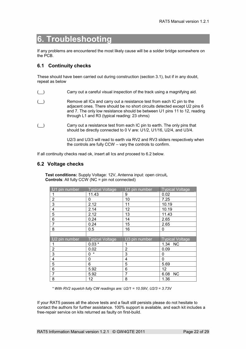
6. Troubleshooting If any problems are encountered the most likely cause will be a solder bridge somewhere on the PCB.
6.1 Continuity checks These should have been carried out during construction (section 3.1), but if in any doubt, repeat as below
(__) Carry out a careful visual inspection of the track using a magnifying aid. (__) Remove all ICs and carry out a resistance test from each IC pin to the
adjacent ones. There should be no short circuits detected except U2 pins 6 and 7. The only low resistance should be between U1 pins 11 to 12, reading through L1 and R3 (typical reading: 23 ohms)
(__) Carry out a resistance test from each IC pin to earth. The only pins that
should be directly connected to 0 V are: U1/2, U1/16, U2/4, and U3/4.
U2/3 and U3/3 will read to earth via RV2 and RV3 sliders respectively when the controls are fully CCW – vary the controls to confirm.
If all continuity checks read ok, insert all Ics and proceed to 6.2 below.
6.2 Voltage checks
Test conditions: Supply Voltage: 12V, Antenna input: open circuit, Controls: All fully CCW (NC = pin not connected)
U1 pin number Typical Voltage U1 pin number Typical Voltage
1 11.43 9 0.02
2 0 10 7.25
3 2.12 11 10.19
4 2.14 12 10.19
5 2.12 13 11.43
6 0.24 14 2.65
7 0.24 15 2.65
8 0.5 16 0
U2 pin number Typical Voltage U3 pin number Typical Voltage
1 0.03 * 1 1.34 NC
2 0.02 2 0.09
3 0 * 3 0
4 0 4 0
5 6 5 5.69
6 5.92 6 12
7 5.92 7 6.08 NC
8 12 8 1.36
* With RV2 squelch fully CW readings are: U2/1 = 10.59V, U2/3 = 3.73V
If your RAT5 passes all the above tests and a fault still persists please do not hesitate to contact the authors for further assistance. 100% support is available, and each kit includes a free-repair service on kits returned as faulty on first-build.
RAT5 Manual version 1.2.1
RAT5 Information Manual version 1.2.1 © GW4GTE 2011 Page 23 of 29
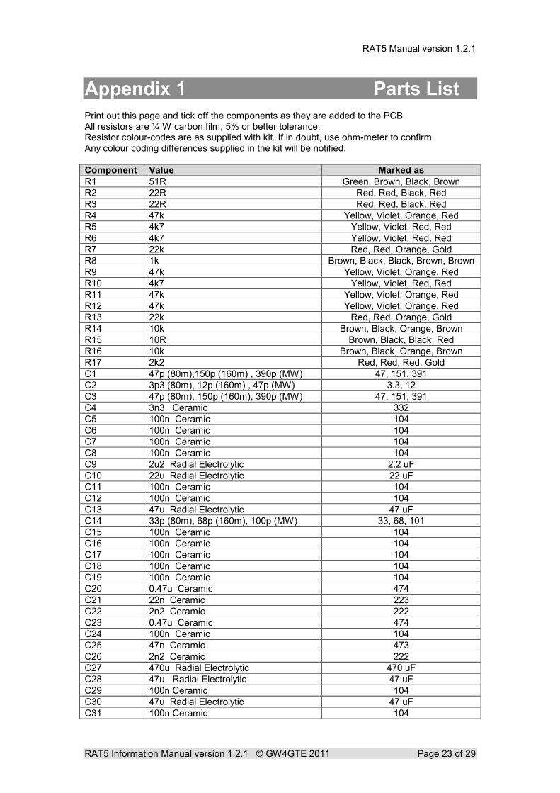
Appendix 1 Parts List Print out this page and tick off the components as they are added to the PCB All resistors are ¼ W carbon film, 5% or better tolerance. Resistor colour-codes are as supplied with kit. If in doubt, use ohm-meter to confirm. Any colour coding differences supplied in the kit will be notified.
Component Value Marked as
R1 51R Green, Brown, Black, Brown
R2 22R Red, Red, Black, Red
R3 22R Red, Red, Black, Red
R4 47k Yellow, Violet, Orange, Red
R5 4k7 Yellow, Violet, Red, Red
R6 4k7 Yellow, Violet, Red, Red
R7 22k Red, Red, Orange, Gold
R8 1k Brown, Black, Black, Brown, Brown
R9 47k Yellow, Violet, Orange, Red
R10 4k7 Yellow, Violet, Red, Red
R11 47k Yellow, Violet, Orange, Red
R12 47k Yellow, Violet, Orange, Red
R13 22k Red, Red, Orange, Gold
R14 10k Brown, Black, Orange, Brown
R15 10R Brown, Black, Black, Red
R16 10k Brown, Black, Orange, Brown
R17 2k2 Red, Red, Red, Gold
C1 47p (80m),150p (160m) , 390p (MW) 47, 151, 391
C2 3p3 (80m), 12p (160m) , 47p (MW) 3.3, 12
C3 47p (80m), 150p (160m), 390p (MW) 47, 151, 391
C4 3n3 Ceramic 332
C5 100n Ceramic 104
C6 100n Ceramic 104
C7 100n Ceramic 104
C8 100n Ceramic 104
C9 2u2 Radial Electrolytic 2.2 uF
C10 22u Radial Electrolytic 22 uF
C11 100n Ceramic 104
C12 100n Ceramic 104
C13 47u Radial Electrolytic 47 uF
C14 33p (80m), 68p (160m), 100p (MW) 33, 68, 101
C15 100n Ceramic 104
C16 100n Ceramic 104
C17 100n Ceramic 104
C18 100n Ceramic 104
C19 100n Ceramic 104
C20 0.47u Ceramic 474
C21 22n Ceramic 223
C22 2n2 Ceramic 222
C23 0.47u Ceramic 474
C24 100n Ceramic 104
C25 47n Ceramic 473
C26 2n2 Ceramic 222
C27 470u Radial Electrolytic 470 uF
C28 47u Radial Electrolytic 47 uF
C29 100n Ceramic 104
C30 47u Radial Electrolytic 47 uF
C31 100n Ceramic 104
RAT5 Manual version 1.2.1
RAT5 Information Manual version 1.2.1 © GW4GTE 2011 Page 24 of 29
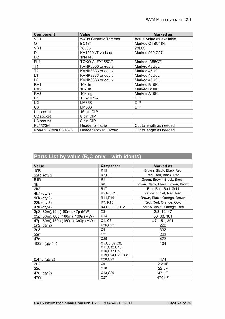
Component Value Marked as
VC1 5-70p Ceramic Trimmer Actual value as available
Q1 BC184 Marked CTBC184
VR1 78L05 78L05
D1 KV1560NT varicap Marked 560.C57
D2 1N4148
FL1 TOKO ALFY455GT Marked A55GT
T1 KANK3333 or equiv Marked 45U0L
T2 KANK3333 or equiv Marked 45U0L
L1 KANK3333 or equiv Marked 45U0L
L2 KANK3333 or equiv Marked 45U0L
RV1 10k lin. Marked B10K
RV2 10k lin. Marked B10K
RV3 10k log. Marked A10K
U1 TDA1072A DIP
U2 LM358 DIP
U3 LM386 DIP
U1 socket 16 pin DIP
U2 socket 8 pin DIP
U3 socket 8 pin DIP
PL1/2/3/4 Header pin strip Cut to length as needed
Non-PCB item SK1/2/3 Header socket 10-way Cut to length as needed
Parts List by value (R,C only – with idents)
Value Component Marked as
10R R15 Brown, Black, Black Red
22R (qty 2) R2,R3 Red, Red, Black, Red
51R R1 Green, Brown, Black, Brown
1k R8 Brown, Black, Black, Brown, Brown
2k2 R17 Red, Red, Red, Gold
4k7 (qty 3) R5,R6,R10 Yellow, Violet, Red, Red
10k (qty 2) R14,R16 Brown, Black, Orange, Brown
22k (qty 2) R7, R13 Red, Red, Orange, Gold
47k (qty 4) R4,R9,R11,R12 Yellow, Violet, Orange, Red
3p3 (80m),12p (160m), 47p (MW) C2 3.3, 12, 47
33p (80m), 68p (160m), 100p (MW) C14 33, 68, 101
47p (80m),150p (160m), 390p (MW) C1, C3 47, 151, 391
2n2 (qty 2) C26,C22 222
3n3 C4 332
22n C21 223
47n C25 473
100n (qty 14) C5,C6,C7,C8, C11,C12,C15, C16,C17,C18, C19,C24,C29,C31
104
0.47u (qty 2) C20,C23 474
2u2 C9 2.2 uF
22u C10 22 uF
47u (qty 2) C13,C30 47 uF
470u C27 470 uF

RAT5 Manual version 1.2.1
RAT5 Information Manual version 1.2.1 © GW4GTE 2011 Page 25 of 29
Appendix 2 Circuit Diagrams

RAT5 Manual version 1.2.1
RAT5 Information Manual version 1.2.1 © GW4GTE 2011 Page 26 of 29
RAT5 Manual version 1.2.1
RAT5 Information Manual version 1.2.1 © GW4GTE 2011 Page 27 of 29
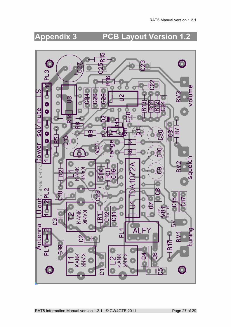
Appendix 3 PCB Layout Version 1.2

RAT5 Manual version 1.2.1
RAT5 Information Manual version 1.2.1 © GW4GTE 2011 Page 28 of 29
Appendix 4 AGC Modification This modification to the squelch circuit was designed by Keith G3XGW and implemented in his Mini-RAT5 receiver pictured below in the builder’s gallery. Impulse noise and most SSB signals will not open the squelch, but a sustained level from a carrier will trigger the squelch after a few seconds. The downside is that the start of an AM transmission is missed, but of course during a QSO the squelch can be left open. R6 is reduced to 1k5, and three components added as shown in the modified circuit below. Squelch triggering is delayed until the 100uF capacitor charges sufficiently via the 150K. The 1N4148 and 1k5 provide a faster discharge path so that the squelch still closes reasonably quickly.
Close-up of the RAT5 modification
RAT5 Manual version 1.2.1
RAT5 Information Manual version 1.2.1 © GW4GTE 2011 Page 29 of 29
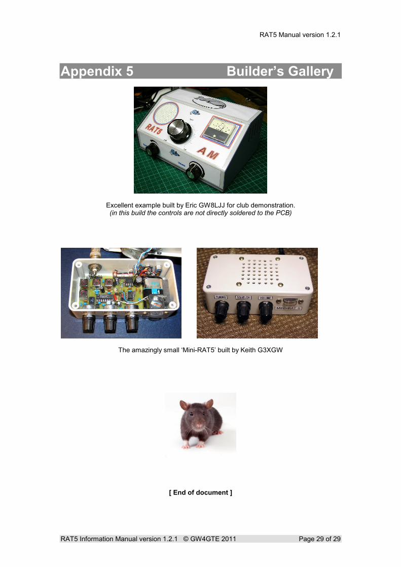
Appendix 5 Builder’s Gallery
Excellent example built by Eric GW8LJJ for club demonstration. (in this build the controls are not directly soldered to the PCB)
The amazingly small ‘Mini-RAT5’ built by Keith G3XGW
[ End of document ]