Embed Size (px)
Citation preview

Available online at www.sciencedirect.com
ls 17 (2008) 105–117www.elsevier.com/locate/diamond
Diamond & Related Materia
Raman and conductivity studies of boron-doped microcrystalline diamond,facetted nanocrystalline diamond and cauliflower diamond films
P.W. May a,⁎, W.J. Ludlow a, M. Hannaway a, P.J. Heard b, J.A. Smith a, K.N. Rosser a
a School of Chemistry, University of Bristol, Bristol BS8 1TS, UKb Interface Analysis Centre, University of Bristol, Oldbury House, 121 St Michael’s Hill, Bristol BS2 8BS, UK
Received 9 July 2007; received in revised form 16 October 2007; accepted 1 November 2007
Available online 13 November 2007
Abstract
We present a large amount of data showing how the electrical conductivity and Raman spectra of boron-doped CVD diamond films vary as afunction of both B content and film type — in particular, diamond crystallite size. Three types of film have been investigated: microcrystallinediamond (MCD), faceted nanocrystalline diamond (f-NCD) and ‘cauliflower’ diamond (c-NCD). For the same B content (measured by SIMS), theconductance of MCD films was much higher than those for the two types of smaller grained films. Multi-wavelength laser Raman spectroscopyshowed that Fano interference effects were much reduced for the smaller grain-sized material. The position of the Lorentzian contribution to the500 cm−1 Raman feature was used to estimate the B content in each type of film, and compared to the value measured using SIMS. We found thatthe Raman method overestimated the concentration of B by a factor of ~5 for the f-NCD and c-NCD films, although it remains reasonablyaccurate for MCD films. The shortfall may be explained if only a small fraction of the B found in the small-grained films is being incorporated intosubstitutional sites. We conclude that in diamond films with a high concentration of grain boundaries, the majority of the B (80% in some cases)must be present at sites that do not contribute to the continuum of electronic states that give rise to metallic conductivity and the Fano effects. Suchsites may include (a) interstitials, (b) the surface of the crystallites, or (c) bonded within the non-diamond carbon impurities present at the grainboundaries. This suggests that heavy doping of nanograined diamond films will give rise to a material with many different conducting regions, andpossibly different conducting pathways and mechanisms.© 2007 Elsevier B.V. All rights reserved.
Keywords: Laser Raman spectroscopy; CVD diamond; nanodiamond; Cauliflower diamond; Boron doping
1. Introduction
Diamond films produced by chemical vapour deposition(CVD) can be doped with boron to produce a p-type semi-conducting material with electrical conductivity that ranges frominsulating to metallic, depending upon the doping level [1]. Theboron dopant atoms act as electron acceptors, and form a bandlocated ~0.35 eV above the valence band edge. At lowtemperatures or at boron concentrations b1017 cm−3 conductionoccurs through holes in the valence band contributed by ionisedsubstitutional B. At higher doping levels, conduction occurs bynearest-neighbour and variable range hopping of holes betweenionised B sites [2], accompanied by a drop inmobility [3]. At very
⁎ Corresponding author.E-mail address: [email protected] (P.W. May).
0925-9635/$ - see front matter © 2007 Elsevier B.V. All rights reserved.doi:10.1016/j.diamond.2007.11.005
high doping levels, an impurity band is formed, giving rise tometal-like conductivity.
A complication is that polycrystalline boron-doped CVDdiamond films possess grain boundaries containing a small-volume fraction of non-diamond carbon impurities. Conse-quently, the electrical conductivity of the film is a complicatedfunction of the combined effects of the boron-doping level, thegrain boundaries, and the impurities. As the grain size in thefilms becomes smaller, i.e. from microcrystalline diamond(MCD) to nanocrystalline diamond (NCD), the relativeimportance of these grain boundaries increases. As a result,most reports concerning B-doped diamond, both fundamentalscience-based and applications-led, have concentrated uponepitaxially-grown diamond or MCD films. There have beenrelatively few studies concerning B-doped NCD films, withthe majority concerning their applications for electrochemical

106 P.W. May et al. / Diamond & Related Materials 17 (2008) 105–117
electrodes [4] or other devices [5,6]. However, a recenttheoretical study by Barnard and Sternberg [7] predicted thatboron is likely to be positioned at the surface of isolatednanoparticles and at the grain boundaries in NCD films.
Unfortunately there is no rigorous definition for NCD in theliterature, and the only agreed property is that the films havegrain sizes in the nm range, typically between 10–500 nm,although even the exact range is arguable. In fact, a number offilms with quite distinct characteristics all come under the broadumbrella of NCD [8]. One type of NCD film is deposited if thedeposition occurs with a very high initial nucleation density(e.g. by using nanodiamond grit for abrasion), followed bystandard growth conditions [9]. These films exhibit columnargrowth, just as for MCD, except with nano-sized crystallites.There is little or no re-nucleation, and the grain size, and henceroughness, increase with film thickness, so above a thickness ofaround 1µm, the film becomes microcrystalline. Thus, theseNCD films can be considered as just smaller grained, facettedversions of MCD, and we shall refer to them as ‘facetted NCD’(f-NCD).
However, this description is not appropriate for many otherNCD films, which often contain a significant fraction of non-diamond material, and exhibit no faceting or evidence ofcolumnar growth, even at thicknesses of several μm. Some NCDfilms have a rounded appearance and as a result, theirmorphology is often referred to as ‘ballas’ (meaning ball-like)or cauliflower-like [10,11]. We shall call these types of films‘cauliflower NCD’ (c-NCD). Thicker c-NCD films can be grownwith essentially flat surfaces with nm smoothness, and thisallows them to be patterned with much higher resolution thanMCD. Decreasing the diamond crystallite size below 10 nmproduces what has come to be known as ‘ultrananocrystalline’diamond (UNCD) films [12]. However, there are as yet noreports of successful B doping of UNCD [13]. In this paper weshall concentrate upon comparing the doping behaviour,electrical properties, and Raman characteristics of boron-doped MCD, f-NCD and c-NCD films.
Studies of the Raman spectra from B-doped diamond filmshave also been restricted almost exclusively to epitaxial orMCD films [14]. The diamond phonon observed at 1332 cm−1
is a symmetric Lorentzian at low boron concentration, but as theboron concentration increases above a threshold of ~1020 cm− 3
— corresponding to the onset of metallic conductivity — thereis an abrupt and pronounced change toward an asymmetricFano-like lineshape [15]. This asymmetry is caused by aquantum mechanical interference between the zone-centreRaman-active optical phonon and the continuum of electronicstates induced by the presence of the dopant. The threshold forthe appearance of the Fano-like lineshape was found to dependon the excitation laser wavelength [16]. The Raman peak alsoshifts to lower wavenumber with increased boron concentration,and is accompanied by a wide signal (300–1330 cm−1) withstructures around 500 and 1225 cm−1 (although these structuresdo not appear when using ultraviolet (244 cm−1) excitation[17]). Such results were first reported for epitaxially-growndiamond [18,19] and then confirmed [15,20] for polycrystallineboron-doped films. Wang et al. [17] found that this shift in the
peak position was also a function of excitation wavelength inthe range 244–514 nm. The origin of the 500 and 1225 cm−1
peaks is uncertain, but their positions approximately agree withtwo maxima in the phonon density of states (PDOS). They maytherefore be connected with a relaxation of the wavevectorselection rules, and if so, they may well be associated with theactual boron incorporation in the lattice, rather than the holeconcentration [21]. There is also evidence [22] that the500 cm−1 peak originates from local vibrational modes ofboron pairs [23], which cause some distortion in the diamondlattice around these isolated defects. Alternatively, peaks similarto these have been seen in the Raman spectra of nanocrystallinediamond films, and assigned to amorphous sp3-bonded carbon[24].
For very heavy B doping, the Fano parameters saturate and itbecomes difficult to discern the position of the zone-centrephonon, with the peaks at 500 and 1225 cm−1 dominating thespectrum. For these conditions, the 500 cm−1 peak can be fittedwith a combination of Gaussian and Lorentzian line shapes. Thewavenumber position, ω, of the Lorentzian componentapproximately obeys [21]:
B½ �=cm�3 ¼ 8:44� 1030 exp �0:048xð Þ ð1Þwhere ω is in cm−1 and the boron content, [B], is in the rangefrom 2×10²⁰ to 1×1022 cm−3.
Here, we present results for the Raman spectra of boron-doped MCD, f-NCD and c-NCD films, as a function of Bcontent, using a range of excitation wavelengths from theultraviolet to the infrared, and extend the findings reported inour preliminary letters paper [25].
2. Experimental
The three types of diamond film were all grown in a standardhot filament CVD reactor using CH4/H2 process gases at apressure of 20 Torr. The substrate was undoped single crystal(100) Si, abraded ultrasonically before deposition using a slurryof 100 nm diamond grit in water. Rhenium was used for thefilament material rather than tantalum since Re does not act as asink for carbon or boron species, unlike Ta which can absorbsignificant amounts of B and C for many hours into thedeposition run [26]. The filament temperature was kept constantat 2400 °C and monitored using a 2-colour optical pyrometer,and the substrate temperature was maintained at ~900 °C.Diborane (B2H6) gas diluted in H2 was used as the source of Bat concentrations between 10–12000 ppm with respect to CH4.All three gases were metered into the chamber using mass flowcontrollers.
For MCD and f-NCD, a ratio of 1%CH4/H2 was used,whereas for c-NCD the methane concentration was increased to5%. The only difference between MCD and f-NCD was that forf-NCD the ultrasonic abrasion was performed for much longerto ensure high nucleation density, and the film growth wasstopped after 90 min to give a continuous film b1 μm thick withsmall facetted grains. MCD and c-NCD films were grown for8 h giving films ~4 μm thick. The various film morphologies

Fig. 1. Scanning electron micrographs of the surface of the three types of diamond film: (a) MCD, showing randomly-oriented grain sizes around 0.5–1 μm, (b) f-NCD, with grain sizes ~100–500 nm, and (c) and (d) c-NCD, with grains sizes 20–100 nm.
Fig. 2. An example of a PL background subtraction from the Raman spectrum ofa very lightly doped f-NCD film viewed using 514 nm (green) excitation. Thedashed line is the fitted PL background.
107P.W. May et al. / Diamond & Related Materials 17 (2008) 105–117
can be seen in Fig. 1. Undoped films were grown in a differentbut otherwise identical HF CVD reactor that had never usedboron-containing gases. This is because B is known to diffuseinto the sidewalls and components within a reactor, and thendiffuse out again during later growth runs, inadvertentlyintroducing B into the gas mixture and causing unwanteddoping of any growing film. Use of a ‘clean’ B-free reactorremoves this risk and allows films with zero B content to bedeposited. Ironically, the fact that B diffuses out of the chamberwalls of the reactor used for B doping during deposition, evenwhen no B2H6 was added to the gas mixture, was useful toproduce films with very low B doping, although controlling thedoping levels in this case was hit-and-miss.
Electrical conductivity measurements were made by both two-point and four-point probe methods. In these, spring-loadedprobes were pressed into contact with the surface of the film andthe resistance measured over a distance of ~ 5 mm. Note that eventhough the four-point probe measurements supposedly removemost of the effects of contact resistance, thesemeasurements wereof the effective surface conductivity, and might not correspond tothe bulk conductivity. The 4-point resistance measurementscould, in principle, be converted to resistivity values in Ω persquare, if the thickness of each of the filmswere known.However,since (a) the thickness varies from sample to sample, (b) there isquite a bit of uncertainty regarding what the true thickness is forvery thin films, and (c) the conductivity is not uniform throughoutthe entire thickness of the film (the surface is likely to be moreconducting than the bulk), this conversion would not yieldaccurate or useful values. Linear plots of current against applied
voltage, passing through the origin, were obtained, showing thatthe contacts were Ohmic.
Boron content within the film was measured using secondaryion mass spectrometry (SIMS), with the B:C count ratio beingcalibrated with respect to those from two reference samples. Thefirst reference was a single crystal diamond implanted with aknown dosage of B, and therefore containing a known B con-tent. The second reference was an undoped CVD diamond film

Table 1B content as measured by SIMS, and as estimated from fitting the 500 cm−1
Raman peak using Eq. ( 1), plus 2-point and 4-point resistance measurements forthe 3 types of films
B content/cm−3
(SIMS)B content/cm−3
(Raman fit)2-pointresistance/Ω
4-pointresistance/Ω
MCDM1 0 – 4.8×10⁷ 7600M2 2.4×10¹⁹ – 1.6×10⁵ 1550M3 7.5×10¹⁹ – 8.1×10⁴ 500M4 3.7×10²⁰ 3.0×10²⁰ 520 81M5 6.0×10²⁰ 4.0×10²⁰ 200 52M6 1.5×10²¹ 7.2×10²⁰ 20 20M7 2.3×10²¹ 1.4×10²¹ 6 9
f-NCDF1 0 – 1×10⁷ 9.0×10⁴
F2 1.5×10²⁰ – 23,000 3800F3 1.4×10²⁰ – 18,000 3700F4 5.0×10²⁰ – 10,000 1000F5 1.3×10²¹ 2.6×10²⁰ 1300 121F6 2.4×10²¹ 3.0×10²⁰ 400 95F7 2.8×10²¹ 8.7×10²⁰ 230 67
c-NCDC1 0 – 2×10⁸ 1×10⁷
C2 6.0×10¹⁸ – 1×10⁷ 5×10⁶
C3 6.1×10²⁰ – 22,000 6480C4 1.1×10²¹ 3.4×10²⁰ 2500 294C5 2.9×10²¹ 4.5×10²⁰ 360 66C6 6.1×10²¹ 9.6×10²⁰ 60 43
The italicised values for SIMS B content for M5, M7 and F4 indicates that thesewere not measured directly, but were interpolated from a plot (Fig. 4) of four-point resistance against B content for the other films in that series.
Fig. 4. B content plotted against measured 4-point conductance (1 / resistance)for the 3 types of films. Filled points are measured SIMS values of B content, thehollow points are estimated values of B content based on inter/extrapolation ofthe trends from the other points. B content values are estimated to be accurate to±10%, as shown by error bars.
108 P.W. May et al. / Diamond & Related Materials 17 (2008) 105–117
with zero B content, providing the background count levelfor B.
Laser Raman spectra were obtained at room temperatureusing a Renishaw 2000 spectrometer and a range of excitation
Fig. 3. Plot of 2-point resistance against 4-point resistance for the 3 typ
wavelengths and lasers: UV 325 nm (HeCd), blue 488 nm(Ar+), green 514 nm (Ar+), red 625 nm HeNe, IR 785 nm (IRdiode), and far IR 830 nm (IR diode). Undoped or lightly dopedfilms often exhibited a large rising or falling photoluminescent(PL) background upon which the much smaller Raman featureswould sit. This PL background would decrease markedly witheven trace amounts of B doping, and for B contentsN5×1018 cm−3 it disappeared altogether giving a flat baseline.The reason for this may be that the B is compensating thenitrogen-related defects within the diamond that give rise to themajority of the PL. Therefore, in order to see the small Ramanfeatures more clearly, and to reproduce the spectra from theundoped films on the same scale as the doped ones, it was usefulto subtract this PL background where necessary. This was done
es of film. Linear lines of best fit have been added to aid the eye.
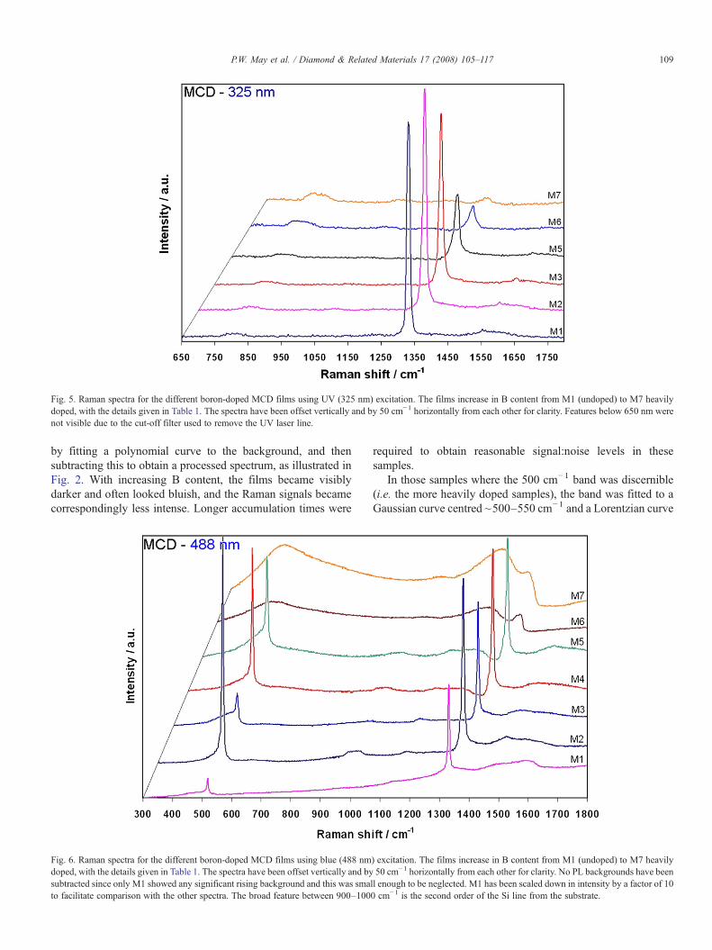
Fig. 5. Raman spectra for the different boron-doped MCD films using UV (325 nm) excitation. The films increase in B content from M1 (undoped) to M7 heavilydoped, with the details given in Table 1. The spectra have been offset vertically and by 50 cm−1 horizontally from each other for clarity. Features below 650 nm werenot visible due to the cut-off filter used to remove the UV laser line.
109P.W. May et al. / Diamond & Related Materials 17 (2008) 105–117
by fitting a polynomial curve to the background, and thensubtracting this to obtain a processed spectrum, as illustrated inFig. 2. With increasing B content, the films became visiblydarker and often looked bluish, and the Raman signals becamecorrespondingly less intense. Longer accumulation times were
Fig. 6. Raman spectra for the different boron-doped MCD films using blue (488 nmdoped, with the details given in Table 1. The spectra have been offset vertically and bysubtracted since only M1 showed any significant rising background and this was smato facilitate comparison with the other spectra. The broad feature between 900–100
required to obtain reasonable signal:noise levels in thesesamples.
In those samples where the 500 cm−1 band was discernible(i.e. the more heavily doped samples), the band was fitted to aGaussian curve centred ~500–550 cm−1 and a Lorentzian curve
) excitation. The films increase in B content from M1 (undoped) to M7 heavily50 cm−1 horizontally from each other for clarity. No PL backgrounds have been
ll enough to be neglected. M1 has been scaled down in intensity by a factor of 100 cm−1 is the second order of the Si line from the substrate.
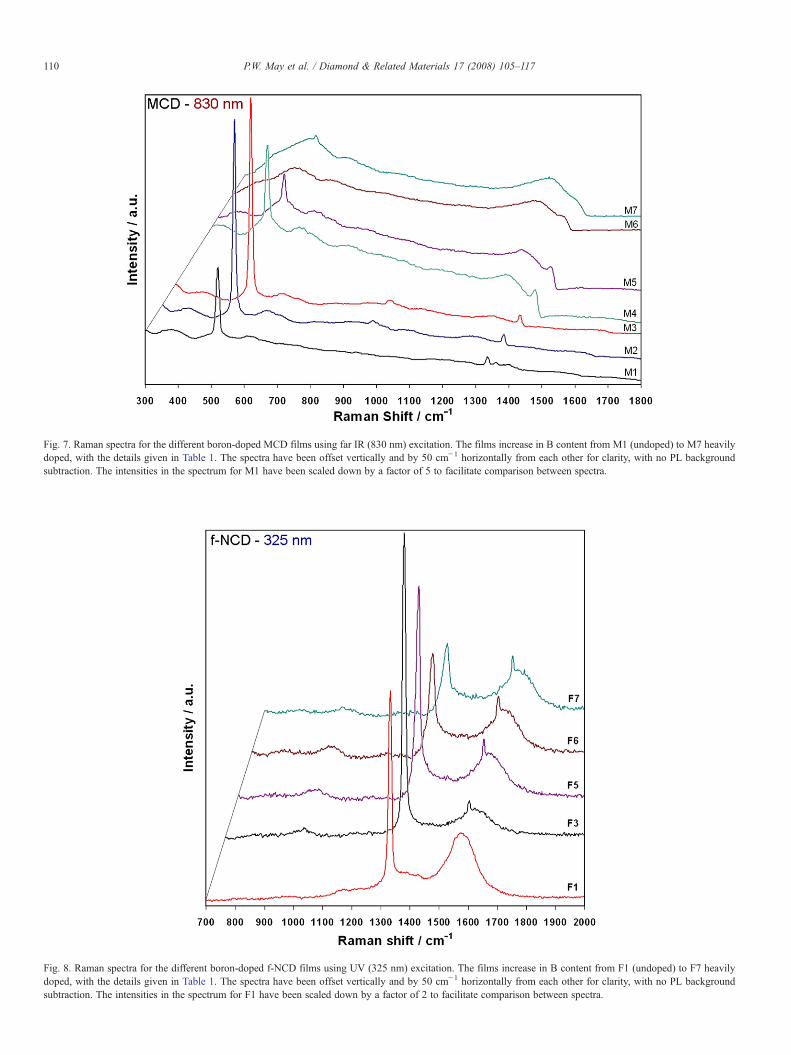
Fig. 7. Raman spectra for the different boron-doped MCD films using far IR (830 nm) excitation. The films increase in B content from M1 (undoped) to M7 heavilydoped, with the details given in Table 1. The spectra have been offset vertically and by 50 cm−1 horizontally from each other for clarity, with no PL backgroundsubtraction. The intensities in the spectrum for M1 have been scaled down by a factor of 5 to facilitate comparison between spectra.
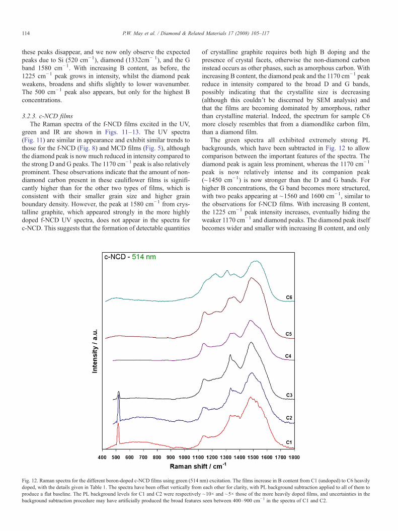
Fig. 8. Raman spectra for the different boron-doped f-NCD films using UV (325 nm) excitation. The films increase in B content from F1 (undoped) to F7 heavilydoped, with the details given in Table 1. The spectra have been offset vertically and by 50 cm−1 horizontally from each other for clarity, with no PL backgroundsubtraction. The intensities in the spectrum for F1 have been scaled down by a factor of 2 to facilitate comparison between spectra.
110 P.W. May et al. / Diamond & Related Materials 17 (2008) 105–117

111P.W. May et al. / Diamond & Related Materials 17 (2008) 105–117
centred ~460–505 cm−1 following the procedure outlined inRef. [21]. Using the relationship between the B content and thewavenumber of the Lorentzian component of the 500 cm−1
band (Eq. (1)), it was possible to estimate the doping levels inthese films, with which to compare the values from SIMS.
3. Results
3.1. Electrical results
The doping levels and resistance values for the 3 sets of filmsare given in Table 1. The undoped MCD and f-NCD films had2-point resistance values in the tens of MΩ, whereas theundoped c-NCD films were much more resistive, havingresistance values N100 MΩ. These values reduced to only afew Ω (i.e. metallic conductivity) for all types of films whenthey were highly doped — a range of 7–8 orders of magnitudein conductivity. The 4-point resistance measurements aresubstantially lower than the 2-point measurements (see Fig.3), showing that the contact resistance for mechanical spring-loaded contacts is significant. As Fig. 3 shows, on a log–logplot the measured 2-point and 4-point values show a roughlylinear dependency, with the gradients of the linear best fit linesincreasing as the crystallite size decreases.
Fig. 9. Raman spectra for the different boron-doped f-NCD films using green (514 ndoped, with the details given in Table 1. The spectra have been offset vertically fromproduce a flat baseline. The intensities in the spectrum for F1 have been scaled downdominates these spectra, and when the spectra are magnified to show the important d900–1000 cm−1 is the second order from this intense Si line.
The values of the boron content in the films are plottedagainst 4-point conductance (=1/resistance) in Fig. 4. Thetrends are roughly linear for all three film types, but theconductance of the MCD films is higher than those for the othertwo films, for the same B doping. This suggests that the dopingefficiency for MCD films is greater than for the other two types,and this might be explained if a greater proportion of theincorporated B atoms were contributing to doping in MCD. In f-NCD and c-NCD films, the reduced doping efficiency suggeststhat a significant amount of the B is being incorporated inpositions (such as at the grain boundaries), which do notimprove the conductivity to the same extent as doping thecrystallites themselves. The incorporation of B at the grainboundary may still affect the overall film conductivity, since‘grain boundary doping’ may provide alternative conductionpathways that compete with the through-grain conduction. Thiswill be explored following more detailed conductivity measure-ments to appear in a subsequent paper.
3.2. Laser Raman spectra
Although laser Raman spectra were obtained for 6 differentlaser wavelengths, only those spectra which show substantialdifferences from each other will be presented here.
m) excitation. The films increase in B content from F1 (undoped) to F7 heavilyeach other for clarity, with PL background subtraction applied to all of them toby a factor of 2 to facilitate comparison between spectra. The Si line at 520 cm−1
etails of the diamond peaks, this Si line goes off scale. The large feature around

112 P.W. May et al. / Diamond & Related Materials 17 (2008) 105–117
3.2.1. MCD filmsThe Raman spectra of the MCD films excited in the UV,
green and far IR are shown in Figs. 5–7. In the UV spectrum(Fig. 5), the diamond peak decreases in intensity and broadenswith increasing B content. The line also exhibits an asymmetricFano lineshape for the samples doped higher than M2 ([B]~2.4×1019 cm3), which is at a smaller doping level than usuallyobserved in epitaxial diamond films [15]. There is a small Gband present with a peak at ~1580 cm−1 due to crystallinegraphite impurities. A new broad feature at ~800 cm−1 isapparent in all these films. Notably, the 1225 cm−1 peak isabsent from the spectrum of even the most highly doped sample,as reported by Wang et al. [17].
The blue Raman spectra (Fig. 6) show trends similar to thoseobserved previously by other groups [15,17,18]. Spectraobtained with green, red and IR excitation are not substantiallydifferent in character to Fig. 6 and so have not been shown herefor brevity. In Fig. 6, the diamond peak shifts to lower wave-number with increasing B content, and the lineshape becomesasymmetric due to Fano interference above a B concentrationof ~3.7×1020 cm3 (sample M4). The broad 1225 cm−1 featureincreases with B concentration and dominates the spectrum athigh B content. The G band is evident at low B concentrations,but is not very intense, and at higher B concentrations, as the filmachieves metallic conductivity (M6 and M7), it disappears. This
Fig. 10. Raman spectra for the different boron-doped f-NCD films using IR (785 nmdoped, with the details given in Table 1. The spectra have been offset vertically fromlarge feature around 900–1000 cm−1 is the second order from the Si line.
does not imply that there is less graphite in these films, onlythat the G band signal is hidden beneath those from the othernearby features. The peak at ~1150 cm−1, which is normallycharacteristic of nanophase diamond but is probably due tosp2 C species at grain boundaries [27], is weakly present for theundoped film, but increases with B concentration, suggestingthat B promotes the incorporation of sp2 carbon species,probably at grain boundaries. At even higher B concentrations,this peak is hidden beneath the 1225 cm−1 peak. The Si line at520 cm−1 generally decreases in intensity with B concentrationas the films become darker and less transmitting to the bluelaser light, however there is a fluctuation in the trend due tovariations in the laser focusing position. The broad featurecentred at ~500 cm−1 becomes more intense with increasing B,and shifts to higher wavenumber (as mentioned by ref.[16]),eventually swamping the Si peak.
The far IR spectra (Fig. 7) show similar features to the blueones, with the diamond peak shifting to lower wavenumber andattaining a Fano lineshape with increasing B content. The1225 cm−1 feature has become much more intense at lower Bconcentrations, and even by sample M4 ([B] ~3.7×1020 cm3)dominates the high wavenumber region of the spectrum. The500 cm−1 feature increases with B content, and a new feature at~600 cm−1, which is weakly present in the spectrum from theundoped sample, also increases with B content.
) excitation. The films increase in B content from F1 (undoped) to F7 heavilyeach other for clarity, with PL background subtraction applied to F1 only. The

Fig. 11. Raman spectra for the different boron-doped c-NCD films using UV (325 nm) excitation. The films increase in B content from C1 (undoped) to C6 heavilydoped, with the details given in Table 1. The spectra have been offset vertically from each other for clarity, with no PL background subtraction.
113P.W. May et al. / Diamond & Related Materials 17 (2008) 105–117
3.2.2. f-NCD filmsThe Raman spectra of the f-NCD films excited in the UV,
green and IR are shown in Figs. 8, 9 and 10. The UV spectra(Fig. 8) are similar in appearance and trends to those for theMCD films (Fig. 5), except that the G band is more prominentdue to the increased sp2 carbon content at the grain boundaries.There is a peak at 1580 cm−1 due to crystalline graphite, whichbecomes more prominent at higher B content. This suggests thataddition of large amounts of B is accompanied by an increasinggraphitisation at the grain boundaries, although SEM analysisshowed that the size of the grains and morphology did notappear to change appreciably — remaining the same as that inFig. 1(b) for all B concentrations.
The green spectra (Fig. 9) show the diamond line, whichagain became broader, less intense, and shifted to lowerwavenumber with increasing B content. The 1150 cm−1
feature is much more prominent than it was in the spectra forMCD films (Fig. 6), which is consistent with it being due topolymeric sp2 C species at the grain boundaries [27]. Thefeature does not shift position with B concentration. Acompanion peak to this, a broad band centred ~1450 cm−1,and the D peak (~1380 cm−1) are also observed in all spectra,and also do not appear to change with B doping level. The Gband appears to have more structure than before, with at leasttwo broad features centred ~1560 and 1600 cm−1 contributingto the overall shape of the feature. The 1225 cm−1 feature that
dominated the spectra of the highly doped MCD films is stillpresent, but is much less dominant for these f-NCD films, andeven at the highest doping level (F7) the diamond peak and the1225 cm− 1 peak remain separate and distinguishable.The broad feature at ~500 cm−1 is also less intense than forthe MCD films, and is now almost entirely hidden beneath theintense Si line.
The IR spectra (Fig. 10) show a gradual evolution with Bconcentration, except for F1 which at first glance appearsanomalous, since it has a large number of unusual peaks that donot appear in the same place as the other samples. In particular,in the F1 spectrum there are peaks at 500 cm−1 (even thoughthere is no B present), several distinct peaks between 550 and900 cm−1, an intense peak at ~1280 cm−1, no diamond peak,and a feature (presumably the G band) at ~1580 cm−1. Thisspectrum also had a very intense PL background, which hasbeen subtracted for the purposes of comparison with the otherspectra. Unusual features such as these have been noted beforein the IR Raman of thin diamond films [28] grown on Si. Recentwork by ourselves [29] has shown them to be dependent uponfilm thickness, and they disappear above a thickness of ~30 μm,suggesting that the IR laser is probing sp2 C structures at thediamond/Si interface. With even trace amounts of B doping(sample F3), the film becomes sufficiently opaque that the PLbackground reduces in intensity significantly making a PLbackground subtraction unnecessary. At the same time, most of
114 P.W. May et al. / Diamond & Related Materials 17 (2008) 105–117
these peaks disappear, and we now only observe the expectedpeaks due to Si (520 cm−1), diamond (1332cm− 1), and the Gband 1580 cm−1. With increasing B content, as before, the1225 cm−1 peak grows in intensity, whilst the diamond peakweakens, broadens and shifts slightly to lower wavenumber.The 500 cm−1 peak also appears, but only for the highest Bconcentrations.
3.2.3. c-NCD filmsThe Raman spectra of the f-NCD films excited in the UV,
green and IR are shown in Figs. 11–13. The UV spectra(Fig. 11) are similar in appearance and exhibit similar trends tothose for the f-NCD (Fig. 8) and MCD films (Fig. 5), althoughthe diamond peak is now much reduced in intensity compared tothe strong D and G peaks. The 1170 cm−1 peak is also relativelyprominent. These observations indicate that the amount of non-diamond carbon present in these cauliflower films is signifi-cantly higher than for the other two types of films, which isconsistent with their smaller grain size and higher grainboundary density. However, the peak at 1580 cm−1 from crys-talline graphite, which appeared strongly in the more highlydoped f-NCD UV spectra, does not appear in the spectra forc-NCD. This suggests that the formation of detectable quantities
Fig. 12. Raman spectra for the different boron-doped c-NCD films using green (514 ndoped, with the details given in Table 1. The spectra have been offset vertically fromproduce a flat baseline. The PL background levels for C1 and C2 were respectivelybackground subtraction procedure may have artificially produced the broad features
of crystalline graphite requires both high B doping and thepresence of crystal facets, otherwise the non-diamond carboninstead occurs as other phases, such as amorphous carbon. Withincreasing B content, the diamond peak and the 1170 cm−1 peakreduce in intensity compared to the broad D and G bands,possibly indicating that the crystallite size is decreasing(although this couldn’t be discerned by SEM analysis) andthat the films are becoming dominated by amorphous, ratherthan crystalline material. Indeed, the spectrum for sample C6more closely resembles that from a diamondlike carbon film,than a diamond film.
The green spectra all exhibited extremely strong PLbackgrounds, which have been subtracted in Fig. 12 to allowcomparison between the important features of the spectra. Thediamond peak is again less prominent, whereas the 1170 cm−1
peak is now relatively intense and its companion peak(~1450 cm−1) is now stronger than the D and G bands. Forhigher B concentrations, the G band becomes more structured,with two peaks appearing at ~1560 and 1600 cm−1, similar tothe observations for f-NCD films. With increasing B content,the 1225 cm−1 peak intensity increases, eventually hiding theweaker 1170 cm−1 and diamond peaks. The diamond peak itselfbecomes wider and smaller with increasing B content, and only
m) excitation. The films increase in B content from C1 (undoped) to C6 heavilyeach other for clarity, with PL background subtraction applied to all of them to~10× and ~5× those of the more heavily doped films, and uncertainties in theseen between 400–900 cm−1 in the spectra of C1 and C2.

Fig. 13. Raman spectra for the different boron-doped c-NCD films using IR (785 nm) excitation. The films increase in B content from C1 (undoped) to C6 heavilydoped, with the details given in Table 1. The spectra have been offset vertically from each other for clarity, with no PL background subtraction. The intensities in thespectra for C1 and C2 have been scaled down by a factor of 10 to facilitate comparison between spectra. The large feature around 900–1000 cm−1 is the second orderfrom the Si line.
115P.W. May et al. / Diamond & Related Materials 17 (2008) 105–117
shifts a small amount to lower wavelength. The Si peak alsodecreases with B content, until it, too, is hidden by the moreintense 500 cm−1 band.
The IR spectra (Fig. 13) show very few features for low Bcontent films, with just a Si peak and a broad PL backgroundcentred around 1330 cm−1. However, with increasing B, the PLbackground diminishes allowing more features, such as thediamond line, the 1170 cm−1 peak, and the G band to becomeapparent. With further increases in B, the 1225 cm−1 peakgrows in intensity and shifts to higher wavenumber, while thediamond line attains the Fano lineshape. At the same time, theSi line disappears as the 500 cm−1 feature becomes much moreintense.
3.2.4. Multi-wavelength Raman spectra of the heaviest dopedfilms
It is worthwhile comparing directly the Raman spectra of theheaviest B-doped films as a function of excitation wavelength,and this is shown in Fig. 14. For the heavily B-doped MCD film(sample M7), the UV spectrum is clearly different to the others,with features at 800 and 1050 cm−1, as well as the graphite peakat 1550 cm−1 appearing here and not in the other spectra. For allthe other spectra there is a clear trend with the 1225 cm−1 peakgradually shifting to higher wavenumber, whilst the diamondpeak shifts to lower wavenumber and broadens. The relativeintensity of the 500 cm−1 peak increases with increasing laser
wavelength. This is also true for the f-NCD spectra (sample F7),with the diamond peak well resolved in the UV spectrum, buthaving merged into the large 1225 cm−1 peak in the IRspectrum. For the c-NCD spectra (sample C6), the diamondpeak is not well resolved in either the UVor the green spectra,and is only really apparent as a shoulder on the 1225 cm−1 peakin the IR spectrum.
Fig. 15 shows the position of the diamond peak for theheaviest doped samples as a function of excitation wavelength.For the heavily B-doped MCD sample, the peak position shiftsto lower wavenumber with increasing laser wavelength, asnoted by Wang et al. [17]. For the f-NCD films, this shift is lesssevere, and for the c-NCD films there is no apparent shift,within the resolution of the Raman spectrometer. This suggeststhat the Fano-type interference of the diamond line is a functionof crystallite size, and for nm-sized crystals the effect isdrastically reduced.
3.2.5. Estimation of B content from the 500 cm−1 Raman lineTable 1 shows the values for B concentration for the heavier
doped films estimated from the Raman fit of the 500 cm−1 peakand using Eq. (1). The values for the MCD films are all within afactor of 2 of those measured by SIMS, showing that for MCDfilms, Eq. (1) is quite accurate. However, for the f-NCD filmsthe estimated values are much less accurate, underestimating theSIMS values by factors of between 3 and 10. The same is true
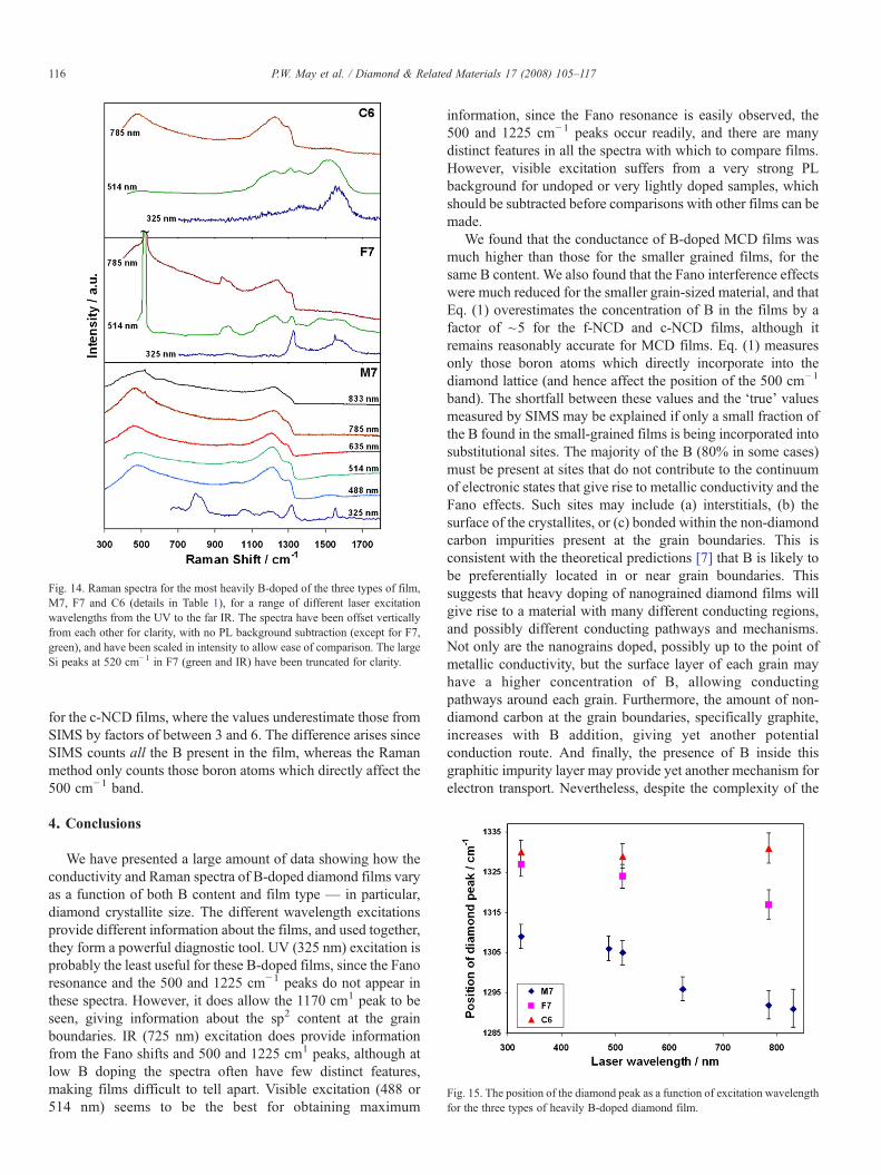
Fig. 15. The position of the diamond peak as a function of excitation wavelengthfor the three types of heavily B-doped diamond film.
Fig. 14. Raman spectra for the most heavily B-doped of the three types of film,M7, F7 and C6 (details in Table 1), for a range of different laser excitationwavelengths from the UV to the far IR. The spectra have been offset verticallyfrom each other for clarity, with no PL background subtraction (except for F7,green), and have been scaled in intensity to allow ease of comparison. The largeSi peaks at 520 cm−1 in F7 (green and IR) have been truncated for clarity.
116 P.W. May et al. / Diamond & Related Materials 17 (2008) 105–117
for the c-NCD films, where the values underestimate those fromSIMS by factors of between 3 and 6. The difference arises sinceSIMS counts all the B present in the film, whereas the Ramanmethod only counts those boron atoms which directly affect the500 cm−1 band.
4. Conclusions
We have presented a large amount of data showing how theconductivity and Raman spectra of B-doped diamond films varyas a function of both B content and film type — in particular,diamond crystallite size. The different wavelength excitationsprovide different information about the films, and used together,they form a powerful diagnostic tool. UV (325 nm) excitation isprobably the least useful for these B-doped films, since the Fanoresonance and the 500 and 1225 cm−1 peaks do not appear inthese spectra. However, it does allow the 1170 cm1 peak to beseen, giving information about the sp2 content at the grainboundaries. IR (725 nm) excitation does provide informationfrom the Fano shifts and 500 and 1225 cm1 peaks, although atlow B doping the spectra often have few distinct features,making films difficult to tell apart. Visible excitation (488 or514 nm) seems to be the best for obtaining maximum
information, since the Fano resonance is easily observed, the500 and 1225 cm−1 peaks occur readily, and there are manydistinct features in all the spectra with which to compare films.However, visible excitation suffers from a very strong PLbackground for undoped or very lightly doped samples, whichshould be subtracted before comparisons with other films can bemade.
We found that the conductance of B-doped MCD films wasmuch higher than those for the smaller grained films, for thesame B content. We also found that the Fano interference effectswere much reduced for the smaller grain-sized material, and thatEq. (1) overestimates the concentration of B in the films by afactor of ~5 for the f-NCD and c-NCD films, although itremains reasonably accurate for MCD films. Eq. (1) measuresonly those boron atoms which directly incorporate into thediamond lattice (and hence affect the position of the 500 cm−1
band). The shortfall between these values and the ‘true’ valuesmeasured by SIMS may be explained if only a small fraction ofthe B found in the small-grained films is being incorporated intosubstitutional sites. The majority of the B (80% in some cases)must be present at sites that do not contribute to the continuumof electronic states that give rise to metallic conductivity and theFano effects. Such sites may include (a) interstitials, (b) thesurface of the crystallites, or (c) bonded within the non-diamondcarbon impurities present at the grain boundaries. This isconsistent with the theoretical predictions [7] that B is likely tobe preferentially located in or near grain boundaries. Thissuggests that heavy doping of nanograined diamond films willgive rise to a material with many different conducting regions,and possibly different conducting pathways and mechanisms.Not only are the nanograins doped, possibly up to the point ofmetallic conductivity, but the surface layer of each grain mayhave a higher concentration of B, allowing conductingpathways around each grain. Furthermore, the amount of non-diamond carbon at the grain boundaries, specifically graphite,increases with B addition, giving yet another potentialconduction route. And finally, the presence of B inside thisgraphitic impurity layer may provide yet another mechanism forelectron transport. Nevertheless, despite the complexity of the

117P.W. May et al. / Diamond & Related Materials 17 (2008) 105–117
underlying conduction mechanisms present in f-NCD and c-NCD films, they can be fabricated with controllable conductiv-ities and nm-smooth surfaces, which might make them idealcandidates for use as an electronic material.
Acknowledgements
The authors would like to thank Jacob Filik, Martin Kubal& Tim Batten, and Keith Hallam & Diana Edwards for useof their far IR, blue, and red Raman systems, respectively,Jonathan Jones for the high resolution SEM photos, and UlrikaDhaenens-Johansson of the University of Warwick for helpwith some of the Raman peak assignments.
References
[1] R. Kalish, Carbon 37 (1999) 781.[2] B. Massarani, J.C. Bourgoin, R.M. Chrenko, Phys. Rev. B 17 (1978) 1758.[3] K. Nishimura, K. Das, J.T. Glass, J. Appl. Phys. 69 (1991) 3142.[4] Yu. V. Pleskov, Russ. J. Electrochem. 38 (2002) 1275.[5] M. Willander, M. Friesel, Q.-ul. Wahab, B. Straumal, J. Mater. Sci: Maters
in Electron. 17 (2006) 1.[6] D.L. Dreifus, A. Collins, T. Humphreys, K. Das, P.E. Pehrsson (Eds.),
Diamond for Electronic Applications, MRS Symp. Proc., vol 416,Materials Research Society, Pittsburgh, 1996.
[7] A.S. Barnard, M. Strernberg, J. Phys. Chem. B 110 (2006) 19307.[8] P.W. May, Chemical vapour deposition — a route to microcrystalline,
nanocrystalline, ultrananocrystalline and single crystal diamond films,Chapter in: Carbon Based Nanomaterials, A. Öchsner, W. Ahmed(Eds.) (Trans Tech, Switzerland, in press).
[9] O.A. Williams, M. Daenen, J. D’Haen, K. Haenen, J. Maes, V.V.Moshchalkov, M. Nesládek, D.M. Gruen, Diamond Relat. Maters. 15(2006) 654.
[10] E. Kohn, P. Gluche, M. Adamschik, Diamond Relat. Maters. 8 (1999) 934.
[11] F.J.H. Guillen, K. Janischowsky, J. Kusterer, W. Ebert, E. Kohn, DiamondRelat. Maters. 14 (2005) 411.
[12] D.M. Gruen, O.A. Shenderova, A.Ya. Vul’ (Eds.), Synthesis, Propertiesand Applications of Ultrananocrystalline Diamond, NATO Science Seriespart II, vol. 192. (Springer, 2005).
[13] P.W. May, M. Hannaway, Mat. Res. Symp. Proc. PV-956 (2006)0956–J09-31.
[14] S. Prawer, R.J. Nemanich, Phil. Trans. R. Soc. Lond. A 362 (2004) 2537.[15] J.W. Ager III, W. Walukiewicz, M. McCluskey, M.A. Plano, M.I.
Landstrass, Appl. Phys. Lett. 66 (1995) 616.[16] F. Pruvost, E. Bustarret, A. Deneuville, Diamond Relat. Mater. 9 (2000)
295.[17] Y.G. Wang, S.P. Lau, B.K. Tay, X.H. Zhang, J. Appl. Phys. 92 (2002)
7253.[18] E. Gheeraert, P. Gonon, A. Deneuville, L. Abello, G. Lucazeau, Diamond
Relat. Mater. 2 (1993) 742.[19] P. Gonon, E. Gheeraert, A. Deneuville, L. Abello, G. Lucazeau, J. Appl.
Phys. 78 (1995) 7059.[20] R. Locher, J. Wagner, F. Fuchs, M. Maier, P. Gonon, P. Koidl, Diamond
Relat. Mater. 4 (1995) 678.[21] M. Bernard, A. Deneuville, P. Muret, Diamond Relat. Mater. 13 (2004)
282.[22] M. Bernard, C. Baron, A. Deneuville Diamond Relat. Mater. 13 (2004)
896.[23] J.P. Goss, P.R. Briddon, Phys. Rev. B 73 (2006) 085204.[24] S. Prawer, K.W. Nugent, D.N. Jamieson, J.O. Orwa, L.A. Bursill, J.L.
Peng, Chem. Phys. Lett. 332 (2000) 93.[25] P.W. May, W.J. Ludlow, M. Hannaway, P.J. Heard, J.A. Smith, K.N.
Rosser, Chem. Phys. Lett. 446 (2007) 103.[26] D.W. Comerford, A. Cheesman, T.P.F. Carpenter, D.M.E. Davies, N.A.
Fox, R.S. Sage, J.A. Smith, M.N.R. Ashfold, Yu. A. Mankelevich, J. Phys.Chem. A 110 (2006) 2868.
[27] A.C. Ferrari, J. Robertson, Phys. Rev. B 63 (2001) 121405.[28] S.M. Leeds, T.J. Davis, P.W. May, C.D.O. Pickard, M.N.R. Ashfold,
Diamond Relat. Mater. 7 (1998) 233.[29] P.W. May, J.A. Smith, K.N. Rosser, Diamond Relat. Mater. (submitted for
publication).