Embed Size (px)
Citation preview

1©2021 Renesas Electronics Corporation May 18, 2021
DescriptionThe 8V19N850 is a fully integrated Radio Unit Clock Synchronizer and Converter Clock Generator designed as a high-performance clock solution for phase/frequency synchronization and signal conditioning of wireless base station radio equipment. The device supports JESD204B/C subclass 0 and 1 device clocks and SYSREF synchronization for converters.
The 8V19N850 supports two independent frequency domains: one that can be used for the digital clock (Ethernet and FEC rates) domain with four outputs, and the device clock (RF-PLL) domain with 12 outputs. The Ethernet domain generates frequencies from two independent APLLs for flexibility; the outputs of the RF clock domain generate very low phase noise clocks for ADC/DAC circuits.
From the integrated RF-PLL, the device supports the clock generation of high-frequency device clocks for driving ADC/DAC devices low-frequency synchronization signals (SYSREF).
A dual DPLL front-end architecture supports any frequency translation. Each DPLL provides a programmable bandwidth and a DCO function for real-time frequency/phase adjustments. The DPLLs can lock on 1PPS input signals and establish lock within 100s or less. Frequency information can be applied from DPLL-0 to DPLL-1 and vice versa to enable the combining of the frequency characteristics of two references (combo-mode).
The 8V19N850 is configured through a pin-mapped I3CSM (including legacy I2C) and 3/4-wire SPI interface. I2C with master capabilities reads a default configuration from an external ROM device. GPIO ports can be configured for reporting and controlling purposes.
Applications Wireless infrastructure 5G radio
Simplified Block Diagram
Features High-performance radio clock synchronizer clock
— Device clock domain (RF-PLL) with support for JESD204B/C
— Digital clock domain (Ethernet, FEC) with support for eEEC and T-BC/T-TSC Class C
2 differential clock reference inputs
— 1PPS (1Hz) to 1GHz input frequency
Dual DPLL front-end with independent clock paths
— External control of the DCO for IEEE1588
— Digital holdover with a 1.1 × 10⁻⁷ ppb accuracy
— Programmable DPLL loop bandwidth 1mHz - 6kHz
— Configurable phase delay (range: 1UI)
— Hitless input switching with < 1ns output phase error
Reference monitors for input LOS, activity and frequency
1 external synchronization input for JESD204B/C (LVCMOS)
16 differential outputs
Dedicated phase management capabilities
Optimized for low phase noise:
— Device clocks: -149.9dBc/Hz (1MHz offset; 245.76MHz clock)
Supply voltage (core): 3.3V; (outputs): 3.3V, 2.5V, and 1.8V
Package: 10 × 10 mm 88-VFQFPN
Board temperature range: -40°C to +105°C
Applicable Standards ITU-T G.8262 EEC1/2, G.8262.1 eEEC
ITU-T G.8273.2 T-BC/T-TSC Class C
JESD204B and C
4 DifferentialClock Outputs≤1GHz
DPLL-0/APLL-0
DPLL-1/APLL-1
APLL-2
RF-PLL
4 Output ChannelsFrequency Dividers
Phase Delay
6 RF Output ChannelsClock + SYSREF
Frequency DividersPhase Delay
SYS_DPLL
SYSREF Generator
Register
TCXO/OCXO
Clock 0
Clock 1
SYSREF
DCO CmdsI3C/I2C/SPI
4
6 DifferentialClock Outputs≤2.94912 GHz
6 DifferentialSYSREF Outputs
6
6
8V19N850DDatasheet
Radio Unit Clock Synchronizer and Converter Clock Generator

2©2021 Renesas Electronics Corporation May 18, 2021
8V19N850 Datasheet
Block DiagramFigure 1. Block Diagram
÷NR2
Integer
QCLK_R4nQCLK_R4
QREF_R4nQREF_R4
RF-PLL Channel 2
QCLK_D0nQCLK_D0
REF0
REF1
Ref. Switching
State Machines
LOS, Freq. Monitor
DPLL-1(DCO-1)
GPIO[0:3]
Device Settings & DCO Control
QCLK_D1nQCLK_D1
÷ND0
QCLK_D2nQCLK_D2
÷ND2
Integer
QCLK_D3nQCLK_D3
÷ND3
Integer
SYSREFGenerator
Device clock
SYSREF
CLK_0nCLK_0
CLK_1nCLK_1
EXT_SYS
Integer
÷NR3
Integer
QCLK_R5nQCLK_R5
QREF_R5nQREF_R5
RF-PLL Channel 3
÷NR0
Integer
QCLK_R0nQCLK_R0
QREF_R0nQREF_R0
QCLK_R1nQCLK_R1
QREF_R1nQREF_R1
RF-PLL Channel 0
LOS, Freq. Monitor
XO_DPLLnXO_PLL
Boot ConfigurationSDA_MSCL_M I2C Master
Register File GPIOI3C/I2C/SPI
SDI/ADR1SDO/SDA
SCLK/SCLnCS/ADR0
SPI_SEL
GbE+FEC clock
GbE clock
SYS-APLLOSCOSCI
OSCO
DPLL-0(DCO-0)
Combo BusSYS-DPLL
XTAL
TCXO
÷ND1
Integer
÷NR1
Integer
QCLK_R2nQCLK_R2
QREF_R2nQREF_R2
QCLK_R3nQCLK_R3
QREF_R3nQREF_R3
RF-PLL Channel 1
APLL-02.45-
2.58GHz
APLL-13.93216GHz
APLL-2 3.6-3.868GHz
RF-PLL2.94912
GHz
System Clocks
Combo Bus
Combo Bus

3©2021 Renesas Electronics Corporation May 18, 2021
8V19N850 Datasheet
Features (Full List) High-performance radio clock synchronizer clock
Device clock domain (RF-PLL) with support for JESD204B/C
Digital clock domain (Ethernet, FEC) with support for eEEC and T-BC/T-TSC Class C
Dual DPLL front-end with independent clock paths
Compliant to ITU-T G.8262 (EEC1/2), G.8262.1 (eEEC), and G.8273.2 (T-BC/T-TSC)
External control of the DCO for IEEE1588 (with a resolution of 1.1 × 10⁻⁷ ppb)
Reference monitors for input LOS, activity and frequency
Fast lock to input signals, incl. 1PPS lock
Digital holdover with a 1.1 × 10⁻⁷ ppb accuracy
Programmable DPLL loop bandwidth 1mHz - 6kHz
Configurable phase delay (range: 1UI)
Hitless input switching with < 1ns output phase error
2 differential clock reference inputs
LVDS and LVPECL compatible, non-inverted input also supports LVCMOS
1PPS (1Hz) to 1GHz input frequency
1 external synchronization input for JESD204B/C (LVCMOS)
16 differential outputs
12 device clock domain outputs (from RF-PLL), 6 clock and 6 SYSREF outputs
4 digital clock domain outputs
Low-power LVPECL/LVDS outputs support configurable signal amplitude, DC and AC coupling and LVPECL, LVDS line terminations techniques
Device clock outputs programmable in output amplitude
Frequency range: 0.4608MHz–2.94912GHz (RF-PLL) and up to 1GHz (Digital clocks)
1PPS (Digital clocks) for T-BC/T-TSC
Dedicated phase management capabilities
Static phase delay for every device clock and SYSREF output
Static and dynamically adjustable phase delay in each DPLL
Supports less than ±0.5ns input to output phase offset
Optimized for low phase noise
Device clocks (RF-PLL): -149.9dBc/Hz (1MHz offset; 245.76MHz clock)
Serial interface ports
3/4-wire SPI or 2-wire I3C (including legacy I2C), pin-mapped, for phase/frequency control and other configurations
Single I2C master boot for obtaining a start-up configuration
Serial control I/O voltage: 1.8V (outputs: selectable 1.8/3.3V voltage)
Supply voltage (core): 3.3V; (outputs): 3.3V, 2.5V, and 1.8V
Package: 10 × 10 mm 88-VFQFPN
Board temperature range: -40°C to +105°C

4©2021 Renesas Electronics Corporation May 18, 2021
8V19N850 Datasheet
ContentsDescription . . . . . . . . . . . . . . . . . . . . . . . . . . . . . . . . . . . . . . . . . . . . . . . . . . . . . . . . . . . . . . . . . . . . . . . . . . . . . . . . . . . . . . . . . . . . . . . . . . . . . . 1Applications . . . . . . . . . . . . . . . . . . . . . . . . . . . . . . . . . . . . . . . . . . . . . . . . . . . . . . . . . . . . . . . . . . . . . . . . . . . . . . . . . . . . . . . . . . . . . . . . . . . . . 1Simplified Block Diagram . . . . . . . . . . . . . . . . . . . . . . . . . . . . . . . . . . . . . . . . . . . . . . . . . . . . . . . . . . . . . . . . . . . . . . . . . . . . . . . . . . . . . . . . . . . 1Features . . . . . . . . . . . . . . . . . . . . . . . . . . . . . . . . . . . . . . . . . . . . . . . . . . . . . . . . . . . . . . . . . . . . . . . . . . . . . . . . . . . . . . . . . . . . . . . . . . . . . . . . 1Applicable Standards . . . . . . . . . . . . . . . . . . . . . . . . . . . . . . . . . . . . . . . . . . . . . . . . . . . . . . . . . . . . . . . . . . . . . . . . . . . . . . . . . . . . . . . . . . . . . . 1Block Diagram . . . . . . . . . . . . . . . . . . . . . . . . . . . . . . . . . . . . . . . . . . . . . . . . . . . . . . . . . . . . . . . . . . . . . . . . . . . . . . . . . . . . . . . . . . . . . . . . . . . 2Features (Full List) . . . . . . . . . . . . . . . . . . . . . . . . . . . . . . . . . . . . . . . . . . . . . . . . . . . . . . . . . . . . . . . . . . . . . . . . . . . . . . . . . . . . . . . . . . . . . . . . 3Contents . . . . . . . . . . . . . . . . . . . . . . . . . . . . . . . . . . . . . . . . . . . . . . . . . . . . . . . . . . . . . . . . . . . . . . . . . . . . . . . . . . . . . . . . . . . . . . . . . . . . . . . . 4Pinout . . . . . . . . . . . . . . . . . . . . . . . . . . . . . . . . . . . . . . . . . . . . . . . . . . . . . . . . . . . . . . . . . . . . . . . . . . . . . . . . . . . . . . . . . . . . . . . . . . . . . . . . . . 7Pin Descriptions . . . . . . . . . . . . . . . . . . . . . . . . . . . . . . . . . . . . . . . . . . . . . . . . . . . . . . . . . . . . . . . . . . . . . . . . . . . . . . . . . . . . . . . . . . . . . . . . . . 8Principles of Operation . . . . . . . . . . . . . . . . . . . . . . . . . . . . . . . . . . . . . . . . . . . . . . . . . . . . . . . . . . . . . . . . . . . . . . . . . . . . . . . . . . . . . . . . . . . . 12
Signal Flow . . . . . . . . . . . . . . . . . . . . . . . . . . . . . . . . . . . . . . . . . . . . . . . . . . . . . . . . . . . . . . . . . . . . . . . . . . . . . . . . . . . . . . . . . . . . . . . . 12One and Two Frequency Domains . . . . . . . . . . . . . . . . . . . . . . . . . . . . . . . . . . . . . . . . . . . . . . . . . . . . . . . . . . . . . . . . . . . . . . . . . . 12Three Frequency Domains . . . . . . . . . . . . . . . . . . . . . . . . . . . . . . . . . . . . . . . . . . . . . . . . . . . . . . . . . . . . . . . . . . . . . . . . . . . . . . . . 14
System APLL (SYS-APLL) . . . . . . . . . . . . . . . . . . . . . . . . . . . . . . . . . . . . . . . . . . . . . . . . . . . . . . . . . . . . . . . . . . . . . . . . . . . . . . . . . . . . 15System DPLL (SYS-DPLL) . . . . . . . . . . . . . . . . . . . . . . . . . . . . . . . . . . . . . . . . . . . . . . . . . . . . . . . . . . . . . . . . . . . . . . . . . . . . . . . . . . . . 16Digital PLLs (DPLL-0, DPLL-1) . . . . . . . . . . . . . . . . . . . . . . . . . . . . . . . . . . . . . . . . . . . . . . . . . . . . . . . . . . . . . . . . . . . . . . . . . . . . . . . . . 17
DPLL-0 Frequency Plan . . . . . . . . . . . . . . . . . . . . . . . . . . . . . . . . . . . . . . . . . . . . . . . . . . . . . . . . . . . . . . . . . . . . . . . . . . . . . . . . . . 17DPLL-1 Frequency Plan . . . . . . . . . . . . . . . . . . . . . . . . . . . . . . . . . . . . . . . . . . . . . . . . . . . . . . . . . . . . . . . . . . . . . . . . . . . . . . . . . . 18DPLL-0/DPLL-1 Operation States . . . . . . . . . . . . . . . . . . . . . . . . . . . . . . . . . . . . . . . . . . . . . . . . . . . . . . . . . . . . . . . . . . . . . . . . . . . 19DPLL Loop Bandwidth . . . . . . . . . . . . . . . . . . . . . . . . . . . . . . . . . . . . . . . . . . . . . . . . . . . . . . . . . . . . . . . . . . . . . . . . . . . . . . . . . . . 21Holdover State . . . . . . . . . . . . . . . . . . . . . . . . . . . . . . . . . . . . . . . . . . . . . . . . . . . . . . . . . . . . . . . . . . . . . . . . . . . . . . . . . . . . . . . . . 21Pull-in/Hold-in . . . . . . . . . . . . . . . . . . . . . . . . . . . . . . . . . . . . . . . . . . . . . . . . . . . . . . . . . . . . . . . . . . . . . . . . . . . . . . . . . . . . . . . . . . 22Free-Run Frequency Accuracy . . . . . . . . . . . . . . . . . . . . . . . . . . . . . . . . . . . . . . . . . . . . . . . . . . . . . . . . . . . . . . . . . . . . . . . . . . . . . 22Phase Slope Limiting (PSL) . . . . . . . . . . . . . . . . . . . . . . . . . . . . . . . . . . . . . . . . . . . . . . . . . . . . . . . . . . . . . . . . . . . . . . . . . . . . . . . 22IEEE 1588 Modes of operation . . . . . . . . . . . . . . . . . . . . . . . . . . . . . . . . . . . . . . . . . . . . . . . . . . . . . . . . . . . . . . . . . . . . . . . . . . . . . 22Phase Adjustment through DPLL . . . . . . . . . . . . . . . . . . . . . . . . . . . . . . . . . . . . . . . . . . . . . . . . . . . . . . . . . . . . . . . . . . . . . . . . . . . 26Input Clock Qualification and Reference Selection . . . . . . . . . . . . . . . . . . . . . . . . . . . . . . . . . . . . . . . . . . . . . . . . . . . . . . . . . . . . . . 26Pin Selection Mode . . . . . . . . . . . . . . . . . . . . . . . . . . . . . . . . . . . . . . . . . . . . . . . . . . . . . . . . . . . . . . . . . . . . . . . . . . . . . . . . . . . . . . 27Manual Selection Mode . . . . . . . . . . . . . . . . . . . . . . . . . . . . . . . . . . . . . . . . . . . . . . . . . . . . . . . . . . . . . . . . . . . . . . . . . . . . . . . . . . 27Automatic Input Clock Selection Mode . . . . . . . . . . . . . . . . . . . . . . . . . . . . . . . . . . . . . . . . . . . . . . . . . . . . . . . . . . . . . . . . . . . . . . . 28Reference Switching . . . . . . . . . . . . . . . . . . . . . . . . . . . . . . . . . . . . . . . . . . . . . . . . . . . . . . . . . . . . . . . . . . . . . . . . . . . . . . . . . . . . . 281PPS Fast Lock . . . . . . . . . . . . . . . . . . . . . . . . . . . . . . . . . . . . . . . . . . . . . . . . . . . . . . . . . . . . . . . . . . . . . . . . . . . . . . . . . . . . . . . . 32Input to Output Phase Alignment . . . . . . . . . . . . . . . . . . . . . . . . . . . . . . . . . . . . . . . . . . . . . . . . . . . . . . . . . . . . . . . . . . . . . . . . . . . 32Input Disqualification by GPIO pins . . . . . . . . . . . . . . . . . . . . . . . . . . . . . . . . . . . . . . . . . . . . . . . . . . . . . . . . . . . . . . . . . . . . . . . . . 34
APLL-2 . . . . . . . . . . . . . . . . . . . . . . . . . . . . . . . . . . . . . . . . . . . . . . . . . . . . . . . . . . . . . . . . . . . . . . . . . . . . . . . . . . . . . . . . . . . . . . . . . . . 34Frequency Plan . . . . . . . . . . . . . . . . . . . . . . . . . . . . . . . . . . . . . . . . . . . . . . . . . . . . . . . . . . . . . . . . . . . . . . . . . . . . . . . . . . . . . . . . . 34
Crystal Oscillator Interface (XO_DPLL/nXO_DPLL) . . . . . . . . . . . . . . . . . . . . . . . . . . . . . . . . . . . . . . . . . . . . . . . . . . . . . . . . . . . . . . . . . 35Crystal Interface (OSCI/OSCO) . . . . . . . . . . . . . . . . . . . . . . . . . . . . . . . . . . . . . . . . . . . . . . . . . . . . . . . . . . . . . . . . . . . . . . . . . . . . . . . . 35Digital Frequency Domains . . . . . . . . . . . . . . . . . . . . . . . . . . . . . . . . . . . . . . . . . . . . . . . . . . . . . . . . . . . . . . . . . . . . . . . . . . . . . . . . . . . . 35Converter Clock Domain and RF-PLL . . . . . . . . . . . . . . . . . . . . . . . . . . . . . . . . . . . . . . . . . . . . . . . . . . . . . . . . . . . . . . . . . . . . . . . . . . . . 36
RF-PLL Channel . . . . . . . . . . . . . . . . . . . . . . . . . . . . . . . . . . . . . . . . . . . . . . . . . . . . . . . . . . . . . . . . . . . . . . . . . . . . . . . . . . . . . . . . 36RF-PLL Channel Frequency Divider . . . . . . . . . . . . . . . . . . . . . . . . . . . . . . . . . . . . . . . . . . . . . . . . . . . . . . . . . . . . . . . . . . . . . . . . . 37Configuration for JESD204B Operation . . . . . . . . . . . . . . . . . . . . . . . . . . . . . . . . . . . . . . . . . . . . . . . . . . . . . . . . . . . . . . . . . . . . . . 38Differential Outputs . . . . . . . . . . . . . . . . . . . . . . . . . . . . . . . . . . . . . . . . . . . . . . . . . . . . . . . . . . . . . . . . . . . . . . . . . . . . . . . . . . . . . . 40Output Phase-Delay . . . . . . . . . . . . . . . . . . . . . . . . . . . . . . . . . . . . . . . . . . . . . . . . . . . . . . . . . . . . . . . . . . . . . . . . . . . . . . . . . . . . . 42General Purpose Input/Outputs (GPIOs) . . . . . . . . . . . . . . . . . . . . . . . . . . . . . . . . . . . . . . . . . . . . . . . . . . . . . . . . . . . . . . . . . . . . . 42
Power-up and Internal Reset . . . . . . . . . . . . . . . . . . . . . . . . . . . . . . . . . . . . . . . . . . . . . . . . . . . . . . . . . . . . . . . . . . . . . . . . . . . . . . . . . . . 48
5©2021 Renesas Electronics Corporation May 18, 2021
8V19N850 Datasheet
Power Supply Sequence . . . . . . . . . . . . . . . . . . . . . . . . . . . . . . . . . . . . . . . . . . . . . . . . . . . . . . . . . . . . . . . . . . . . . . . . . . . . . . . . . . 48Automatic Startup and Self-Configuration . . . . . . . . . . . . . . . . . . . . . . . . . . . . . . . . . . . . . . . . . . . . . . . . . . . . . . . . . . . . . . . . . . . . . 48
Serial Port Description . . . . . . . . . . . . . . . . . . . . . . . . . . . . . . . . . . . . . . . . . . . . . . . . . . . . . . . . . . . . . . . . . . . . . . . . . . . . . . . . . . . . . . . . 54SPI Interface (SPI_SEL = 1) . . . . . . . . . . . . . . . . . . . . . . . . . . . . . . . . . . . . . . . . . . . . . . . . . . . . . . . . . . . . . . . . . . . . . . . . . . . . . . . 54I3C Interface (SPI_SEL = 0) . . . . . . . . . . . . . . . . . . . . . . . . . . . . . . . . . . . . . . . . . . . . . . . . . . . . . . . . . . . . . . . . . . . . . . . . . . . . . . . 57I2C Master Interface . . . . . . . . . . . . . . . . . . . . . . . . . . . . . . . . . . . . . . . . . . . . . . . . . . . . . . . . . . . . . . . . . . . . . . . . . . . . . . . . . . . . . 58
Configuration and Status Registers . . . . . . . . . . . . . . . . . . . . . . . . . . . . . . . . . . . . . . . . . . . . . . . . . . . . . . . . . . . . . . . . . . . . . . . . . . . . . . . . . . 60General Device Configuration . . . . . . . . . . . . . . . . . . . . . . . . . . . . . . . . . . . . . . . . . . . . . . . . . . . . . . . . . . . . . . . . . . . . . . . . . . . . . . . . . . 60General Power Down Registers . . . . . . . . . . . . . . . . . . . . . . . . . . . . . . . . . . . . . . . . . . . . . . . . . . . . . . . . . . . . . . . . . . . . . . . . . . . . . . . . 62Read EEPROM Status . . . . . . . . . . . . . . . . . . . . . . . . . . . . . . . . . . . . . . . . . . . . . . . . . . . . . . . . . . . . . . . . . . . . . . . . . . . . . . . . . . . . . . . 63I/O Voltage Select Configuration . . . . . . . . . . . . . . . . . . . . . . . . . . . . . . . . . . . . . . . . . . . . . . . . . . . . . . . . . . . . . . . . . . . . . . . . . . . . . . . . 63System APLL (SYS-APLL) Configuration . . . . . . . . . . . . . . . . . . . . . . . . . . . . . . . . . . . . . . . . . . . . . . . . . . . . . . . . . . . . . . . . . . . . . . . . . 64System DPLL (SYS-DPLL) Configuration . . . . . . . . . . . . . . . . . . . . . . . . . . . . . . . . . . . . . . . . . . . . . . . . . . . . . . . . . . . . . . . . . . . . . . . . . 65System DPLL (SYS-DPLL) Lock Threshold, Lock Timer, Bandwidth . . . . . . . . . . . . . . . . . . . . . . . . . . . . . . . . . . . . . . . . . . . . . . . . . . . . 66System DPLL (SYS-DPLL) Phase Error Compensation (PEC) and Frequency Divider . . . . . . . . . . . . . . . . . . . . . . . . . . . . . . . . . . . . . . 68Reference Monitor for Input CLK_0 . . . . . . . . . . . . . . . . . . . . . . . . . . . . . . . . . . . . . . . . . . . . . . . . . . . . . . . . . . . . . . . . . . . . . . . . . . . . . . 69Reference Monitor for Input CLK_1 . . . . . . . . . . . . . . . . . . . . . . . . . . . . . . . . . . . . . . . . . . . . . . . . . . . . . . . . . . . . . . . . . . . . . . . . . . . . . . 73Global Status . . . . . . . . . . . . . . . . . . . . . . . . . . . . . . . . . . . . . . . . . . . . . . . . . . . . . . . . . . . . . . . . . . . . . . . . . . . . . . . . . . . . . . . . . . . . . . . 77DPLL-0 (APLL-0) Frequency Configuration . . . . . . . . . . . . . . . . . . . . . . . . . . . . . . . . . . . . . . . . . . . . . . . . . . . . . . . . . . . . . . . . . . . . . . . 82DPLL-0 (APLL-0) DSM Control and APLL-0 Charge Pump Configuration . . . . . . . . . . . . . . . . . . . . . . . . . . . . . . . . . . . . . . . . . . . . . . . . 84DPLL-0 Feedback Divider M0 . . . . . . . . . . . . . . . . . . . . . . . . . . . . . . . . . . . . . . . . . . . . . . . . . . . . . . . . . . . . . . . . . . . . . . . . . . . . . . . . . . 86DPLL-0 Frequency Control . . . . . . . . . . . . . . . . . . . . . . . . . . . . . . . . . . . . . . . . . . . . . . . . . . . . . . . . . . . . . . . . . . . . . . . . . . . . . . . . . . . . 87DPLL-0 Lock Timer . . . . . . . . . . . . . . . . . . . . . . . . . . . . . . . . . . . . . . . . . . . . . . . . . . . . . . . . . . . . . . . . . . . . . . . . . . . . . . . . . . . . . . . . . . 88DPLL-0 Hitless Switch . . . . . . . . . . . . . . . . . . . . . . . . . . . . . . . . . . . . . . . . . . . . . . . . . . . . . . . . . . . . . . . . . . . . . . . . . . . . . . . . . . . . . . . . 88DPLL-0 Mode Control . . . . . . . . . . . . . . . . . . . . . . . . . . . . . . . . . . . . . . . . . . . . . . . . . . . . . . . . . . . . . . . . . . . . . . . . . . . . . . . . . . . . . . . . 89DPLL-0 Phase Offset, Write Phase and Frequency . . . . . . . . . . . . . . . . . . . . . . . . . . . . . . . . . . . . . . . . . . . . . . . . . . . . . . . . . . . . . . . . . 91DPLL-0 Reference State . . . . . . . . . . . . . . . . . . . . . . . . . . . . . . . . . . . . . . . . . . . . . . . . . . . . . . . . . . . . . . . . . . . . . . . . . . . . . . . . . . . . . . 92DPLL-0 Lock Threshold, Lock Timer, Bandwidth . . . . . . . . . . . . . . . . . . . . . . . . . . . . . . . . . . . . . . . . . . . . . . . . . . . . . . . . . . . . . . . . . . . 94DPLL-0 Phase Slope Limiting . . . . . . . . . . . . . . . . . . . . . . . . . . . . . . . . . . . . . . . . . . . . . . . . . . . . . . . . . . . . . . . . . . . . . . . . . . . . . . . . . . 96DPLL-0 Holdover, Phase Error Compensation (PEC) . . . . . . . . . . . . . . . . . . . . . . . . . . . . . . . . . . . . . . . . . . . . . . . . . . . . . . . . . . . . . . . . 97DPLL-0 Fractional Feedback Divider M1 . . . . . . . . . . . . . . . . . . . . . . . . . . . . . . . . . . . . . . . . . . . . . . . . . . . . . . . . . . . . . . . . . . . . . . . . . 99DPLL-1 (APLL-1) Frequency Configuration . . . . . . . . . . . . . . . . . . . . . . . . . . . . . . . . . . . . . . . . . . . . . . . . . . . . . . . . . . . . . . . . . . . . . . 100DPLL-1 (APLL-1) DSM Control and APLL-1 Charge Pump Configuration . . . . . . . . . . . . . . . . . . . . . . . . . . . . . . . . . . . . . . . . . . . . . . . 102DPLL-1 Lock Timer . . . . . . . . . . . . . . . . . . . . . . . . . . . . . . . . . . . . . . . . . . . . . . . . . . . . . . . . . . . . . . . . . . . . . . . . . . . . . . . . . . . . . . . . . 105DPLL-1 Hitless Switch . . . . . . . . . . . . . . . . . . . . . . . . . . . . . . . . . . . . . . . . . . . . . . . . . . . . . . . . . . . . . . . . . . . . . . . . . . . . . . . . . . . . . . . 105DPLL-1 Mode Control . . . . . . . . . . . . . . . . . . . . . . . . . . . . . . . . . . . . . . . . . . . . . . . . . . . . . . . . . . . . . . . . . . . . . . . . . . . . . . . . . . . . . . . 106DPLL-1 Phase Offset, Write Phase and Frequency . . . . . . . . . . . . . . . . . . . . . . . . . . . . . . . . . . . . . . . . . . . . . . . . . . . . . . . . . . . . . . . . 108DPLL-1 Reference State . . . . . . . . . . . . . . . . . . . . . . . . . . . . . . . . . . . . . . . . . . . . . . . . . . . . . . . . . . . . . . . . . . . . . . . . . . . . . . . . . . . . . 110DPLL-1 Lock Threshold, Lock Timer, Bandwidth . . . . . . . . . . . . . . . . . . . . . . . . . . . . . . . . . . . . . . . . . . . . . . . . . . . . . . . . . . . . . . . . . . 112DPLL-1 Phase Slope Limiting . . . . . . . . . . . . . . . . . . . . . . . . . . . . . . . . . . . . . . . . . . . . . . . . . . . . . . . . . . . . . . . . . . . . . . . . . . . . . . . . . 114DPLL-1 Holdover, Phase Error Compensation (PEC) . . . . . . . . . . . . . . . . . . . . . . . . . . . . . . . . . . . . . . . . . . . . . . . . . . . . . . . . . . . . . . . 115DPLL-1 Fractional Feedback Divider M1 . . . . . . . . . . . . . . . . . . . . . . . . . . . . . . . . . . . . . . . . . . . . . . . . . . . . . . . . . . . . . . . . . . . . . . . . 117APLL-2 Configuration Registers . . . . . . . . . . . . . . . . . . . . . . . . . . . . . . . . . . . . . . . . . . . . . . . . . . . . . . . . . . . . . . . . . . . . . . . . . . . . . . . 118RF-PLL Configuration Registers . . . . . . . . . . . . . . . . . . . . . . . . . . . . . . . . . . . . . . . . . . . . . . . . . . . . . . . . . . . . . . . . . . . . . . . . . . . . . . . 121SYSREF Registers . . . . . . . . . . . . . . . . . . . . . . . . . . . . . . . . . . . . . . . . . . . . . . . . . . . . . . . . . . . . . . . . . . . . . . . . . . . . . . . . . . . . . . . . . 124Channel D0-D3 and R0-R3 Registers . . . . . . . . . . . . . . . . . . . . . . . . . . . . . . . . . . . . . . . . . . . . . . . . . . . . . . . . . . . . . . . . . . . . . . . . . . . 127Output Registers . . . . . . . . . . . . . . . . . . . . . . . . . . . . . . . . . . . . . . . . . . . . . . . . . . . . . . . . . . . . . . . . . . . . . . . . . . . . . . . . . . . . . . . . . . . 134GPIO Registers . . . . . . . . . . . . . . . . . . . . . . . . . . . . . . . . . . . . . . . . . . . . . . . . . . . . . . . . . . . . . . . . . . . . . . . . . . . . . . . . . . . . . . . . . . . . 138Device Status . . . . . . . . . . . . . . . . . . . . . . . . . . . . . . . . . . . . . . . . . . . . . . . . . . . . . . . . . . . . . . . . . . . . . . . . . . . . . . . . . . . . . . . . . . . . . 141
6©2021 Renesas Electronics Corporation May 18, 2021
8V19N850 Datasheet
DPLL-0/DPLL-1/APLL-2/RF-PLL Status . . . . . . . . . . . . . . . . . . . . . . . . . . . . . . . . . . . . . . . . . . . . . . . . . . . . . . . . . . . . . . . . . . . . . . . . . 142Initialization and Internal SYSREF Trigger . . . . . . . . . . . . . . . . . . . . . . . . . . . . . . . . . . . . . . . . . . . . . . . . . . . . . . . . . . . . . . . . . . . . . . . 143Channel Enable and PLL Reference Registers Descriptions . . . . . . . . . . . . . . . . . . . . . . . . . . . . . . . . . . . . . . . . . . . . . . . . . . . . . . . . . 145
Electrical Characteristics . . . . . . . . . . . . . . . . . . . . . . . . . . . . . . . . . . . . . . . . . . . . . . . . . . . . . . . . . . . . . . . . . . . . . . . . . . . . . . . . . . . . . . . . . 147Absolute Maximum Ratings . . . . . . . . . . . . . . . . . . . . . . . . . . . . . . . . . . . . . . . . . . . . . . . . . . . . . . . . . . . . . . . . . . . . . . . . . . . . . . . . . . . 147Pin Characteristics . . . . . . . . . . . . . . . . . . . . . . . . . . . . . . . . . . . . . . . . . . . . . . . . . . . . . . . . . . . . . . . . . . . . . . . . . . . . . . . . . . . . . . . . . 148External Oscillator Characteristics . . . . . . . . . . . . . . . . . . . . . . . . . . . . . . . . . . . . . . . . . . . . . . . . . . . . . . . . . . . . . . . . . . . . . . . . . . . . . 148DC Characteristics . . . . . . . . . . . . . . . . . . . . . . . . . . . . . . . . . . . . . . . . . . . . . . . . . . . . . . . . . . . . . . . . . . . . . . . . . . . . . . . . . . . . . . . . . 149AC Characteristics . . . . . . . . . . . . . . . . . . . . . . . . . . . . . . . . . . . . . . . . . . . . . . . . . . . . . . . . . . . . . . . . . . . . . . . . . . . . . . . . . . . . . . . . . 153
Application Information . . . . . . . . . . . . . . . . . . . . . . . . . . . . . . . . . . . . . . . . . . . . . . . . . . . . . . . . . . . . . . . . . . . . . . . . . . . . . . . . . . . . . . . . . . . 166Termination for QCLK_y, QREF_r LVDS Outputs (STYLE = 0) . . . . . . . . . . . . . . . . . . . . . . . . . . . . . . . . . . . . . . . . . . . . . . . . . . . . . . . 166AC Termination for QCLK_y, QREF_r LVDS Outputs (STYLE = 0) . . . . . . . . . . . . . . . . . . . . . . . . . . . . . . . . . . . . . . . . . . . . . . . . . . . . 166Termination for QCLK_y, QREF_r LVPECL Outputs (STYLE = 1) . . . . . . . . . . . . . . . . . . . . . . . . . . . . . . . . . . . . . . . . . . . . . . . . . . . . . 167Thermal Characteristics . . . . . . . . . . . . . . . . . . . . . . . . . . . . . . . . . . . . . . . . . . . . . . . . . . . . . . . . . . . . . . . . . . . . . . . . . . . . . . . . . . . . . 168
Case Temperature Considerations . . . . . . . . . . . . . . . . . . . . . . . . . . . . . . . . . . . . . . . . . . . . . . . . . . . . . . . . . . . . . . . . . . . . . . . . . 168Package Exposed Pad Thermal Release Path . . . . . . . . . . . . . . . . . . . . . . . . . . . . . . . . . . . . . . . . . . . . . . . . . . . . . . . . . . . . . . . . 169
Package Outline Drawings . . . . . . . . . . . . . . . . . . . . . . . . . . . . . . . . . . . . . . . . . . . . . . . . . . . . . . . . . . . . . . . . . . . . . . . . . . . . . . . . . . . . . . . . 169Marking Diagram . . . . . . . . . . . . . . . . . . . . . . . . . . . . . . . . . . . . . . . . . . . . . . . . . . . . . . . . . . . . . . . . . . . . . . . . . . . . . . . . . . . . . . . . . . . . . . . 169Ordering Information . . . . . . . . . . . . . . . . . . . . . . . . . . . . . . . . . . . . . . . . . . . . . . . . . . . . . . . . . . . . . . . . . . . . . . . . . . . . . . . . . . . . . . . . . . . . 170Glossary . . . . . . . . . . . . . . . . . . . . . . . . . . . . . . . . . . . . . . . . . . . . . . . . . . . . . . . . . . . . . . . . . . . . . . . . . . . . . . . . . . . . . . . . . . . . . . . . . . . . . . 171Errata . . . . . . . . . . . . . . . . . . . . . . . . . . . . . . . . . . . . . . . . . . . . . . . . . . . . . . . . . . . . . . . . . . . . . . . . . . . . . . . . . . . . . . . . . . . . . . . . . . . . . . . . 172Revision History . . . . . . . . . . . . . . . . . . . . . . . . . . . . . . . . . . . . . . . . . . . . . . . . . . . . . . . . . . . . . . . . . . . . . . . . . . . . . . . . . . . . . . . . . . . . . . . . 172
7©2021 Renesas Electronics Corporation May 18, 2021
8V19N850 Datasheet
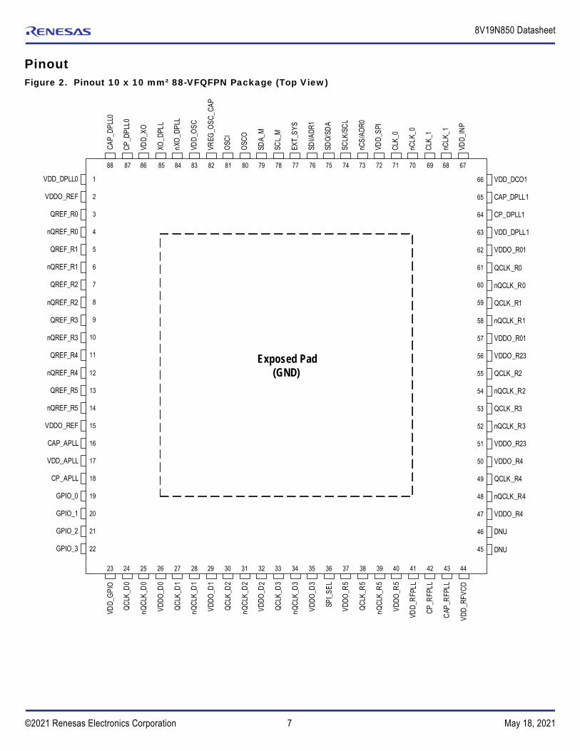
PinoutFigure 2. Pinout 10 x 10 mm² 88-VFQFPN Package (Top View)
Exposed Pad(GND)
1
2
3
4
5
6
7
8
9
10
11
12
13
14
15
16
17
18
19
20
21
22
88 87 86 85 84 83 82 81 80 79 78 77 76 75 74 73 72 71 70 69 68 67
23 24 25 26 27 28 29 30 31 32 33 34 35 36 37 38 39 40 41 42 43 44
66
65
64
63
62
61
60
59
58
57
56
55
54
53
52
51
50
49
48
47
46
45
nQCLK_R4
VDDO_R4
VDD_DCO1
VDDO_R01
nQCLK_R3
VDDO_R23
VDDO_R4
QCLK_R4
DNU
DNU
VDDO_R23
QCLK_R2
nQCLK_R2
QCLK_R3
QCLK_R0
nQCLK_R0
QCLK_R1
nQCLK_R1
CAP_DPLL1
CP_DPLL1
VDD_DPLL1
VDDO_R01
CAP_
DPL
L0
SDA_
M
nCLK
_0
CLK
_1
nCLK
_1
VDD_
INP
SCLK
/SC
L
nCS
/ADR
0
VDD_
SPI
CLK
_0
SCL_
M
EXT_
SYS
SDI/A
DR1
SDO/
SDA
VDD_
OSC
VREG
_OSC
_CAP
OSC
I
OSC
O
CP_D
PLL0
VDD_
XO
XO_D
PLL
nXO
_DPL
LVDD_DPLL0
VDDO_REF
QREF_R0
nQREF_R0
QREF_R1
nQREF_R1
QREF_R2
nQREF_R2
QREF_R5
QREF_R3
nQREF_R3
QREF_R4
nQREF_R4
nQREF_R5
VDDO_REF
CAP_APLL
VDD_APLL
CP_APLL
GPIO_0
GPIO_1
GPIO_2
GPIO_3
VDDO
_D0
nQCL
K_D
0
VDD_
GPI
O
QCL
K_D
0
QCL
K_D
1
nQCL
K_D
1
VDDO
_D1
QCL
K_D
2
VDDO
_D3
VDD
_RFV
CO
nQCL
K_D
2
VDDO
_D2
QCL
K_D
3
nQCL
K_D
3
VDDO
_R5
QCL
K_R
5
nQCL
K_R
5
VDDO
_R5
SPI_
SEL
VDD_
RF P
LL
CP_R
FPLL
CAP
_RFP
LL

8©2021 Renesas Electronics Corporation May 18, 2021
8V19N850 Datasheet
Pin DescriptionsTable 1. Pin Descriptionsa
Pin Name Typeb Description
Signal Inputs
71 CLK_0Input
PD Device clock 0 inverting and non-inverting differential clock input. Inverting input is biased to VDD_V /2 by default when left floating. Compatible with LVPECL, LVDS, and LVCMOS signals.70 nCLK_0 PD/PU
69 CLK_1Input
PD Device clock 1 inverting and non-inverting differential clock input. Inverting input is biased to VDD_V /2 by default when left floating. Compatible with LVPECL, LVDS, and LVCMOS signals.68 nCLK_1 PD/PU
85 XO_DPLL
Input
PD Single-ended or differential crystal oscillator input for the system DPLL (SYS-DPLL) and for the SYS-APLL (selectable). May also be a reference to APLL-0 and APLL-1. For a frequency specification, see Table 132. Inverting input is biased to VDD_V /2 by
default when left floating. Compatible with LVPECL, LVDS, and LVCMOS signals. 84 nXO_DPLL
PD/PU
81 OSCI Input XTAL interface of the system APLL (SYS-APLL) and reference to APLL-0 and APLL-1. It is also a reference for APLL-2 when APLL-2 is used as part of the system DPLL (SYS-DPLL). For a frequency and interface specification, see Table 132. OSCI should be AC-coupled, if an oscillator (XO) is used on OSCI, leave OSCO unconnected.
80 OSCO Output
77 EXT_SYS Input PD External SYSREF pulse trigger input. 1.8V LVCMOS interface levels (3.3V tolerant)
36 SPI_SEL Input PU SPI/I3C Select. 1.8V/2.5V/3.3V LVCMOS interface levels. For levels, see Table 134.
Signal Outputs
61,60
QCLK_R0,nQCLK_R0
Output Differential clock output R0 (Device clock from RF-PLL, Channel 0). Configurable LVPECL/LVDS style, offset voltage and amplitude. 3.3V, 2.5V, or 1.8V output voltage supply.
59,58
QCLK_R1,nQCLK_R1
Output Differential clock output R1 (Device clock from RF-PLL, Channel 0). Configurable LVPECL/LVDS style, offset voltage and amplitude. 3.3V, 2.5V, or 1.8V output voltage supply.
55,54
QCLK_R2,nQCLK_R2
Output Differential clock output R2 (Device clock from RF-PLL, Channel 1). Configurable LVPECL/LVDS style, offset voltage and amplitude. 3.3V, 2.5V, or 1.8V output voltage supply.
53,52
QCLK_R3,nQCLK_R3
Output Differential clock output R3 (Device clock from RF-PLL, Channel 1). Configurable LVPECL/LVDS style, offset voltage and amplitude. 3.3V, 2.5V, or 1.8V output voltage supply.
49,48
QCLK_R4,nQCLK_R4
Output Differential clock output R4 (Device clock from RF-PLL, Channel 2). Configurable LVPECL/LVDS style, offset voltage and amplitude. 3.3V, 2.5V, or 1.8V output voltage supply.
38,39
QCLK_R5,nQCLK_R5
Output Differential clock output R5 (Device clock from RF-PLL, Channel 3). Configurable LVPECL/LVDS style, offset voltage and amplitude. 3.3V, 2.5V, or 1.8V output voltage supply.
3,4
QREF_R0, nQREF_R0
Output Differential SYSREF output R0 (RF-PLL, Channel 0). Configurable LVPECL/LVDS style, offset voltage and amplitude. 3.3V, 2.5V, or 1.8V output voltage supply.

9©2021 Renesas Electronics Corporation May 18, 2021
8V19N850 Datasheet
5,6
QREF_R1, nQREF_R1
Output Differential SYSREF output R1 (RF-PLL, Channel 0). Configurable LVPECL/LVDS style, offset voltage and amplitude. 3.3V, 2.5V, or 1.8V output voltage supply.
7,8
QREF_R2, nQREF_R2
Output Differential SYSREF output R2 (RF-PLL, Channel 1). Configurable LVPECL/LVDS style, offset voltage and amplitude. 3.3V, 2.5V, or 1.8V output voltage supply.
9,10
QREF_R3, nQREF_R3
Output Differential SYSREF output R3 (RF-PLL, Channel 1). Configurable LVPECL/LVDS style, offset voltage and amplitude. 3.3V, 2.5V, or 1.8V output voltage supply.
11,12
QREF_R4, nQREF_R4
Output Differential SYSREF output R4 (RF-PLL, Channel 2). Configurable LVPECL/LVDS style, offset voltage and amplitude. 3.3V, 2.5V, or 1.8V output voltage supply.
13,14
QREF_R5, nQREF_R5
Output Differential SYSREF output R5 (RF-PLL, Channel 3). Configurable LVPECL/LVDS style, offset voltage and amplitude. 3.3V, 2.5V, or 1.8V output voltage supply.
24,25
QCLK_D0, nQCLK_D0
Output Differential clock output D0 (Digital clock). Configurable LVPECL/LVDS/LVCMOS style and amplitude. 3.3V, 2.5V, or 1.8V output voltage.
27,28
QCLK_D1, nQCLK_D1
Output Differential clock output D1 (Digital clock). Configurable LVPECL/LVDS/LVCMOS style and amplitude. 3.3V, 2.5V, or 1.8V output voltage.
30,31
QCLK_D2, nQCLK_D2
Output Differential clock output D2 (Digital clock). Configurable LVPECL/LVDS/LVCMOS style and amplitude. 3.3V, 2.5V, or 1.8V output voltage.
33,34
QCLK_D3, nQCLK_D3
Output Differential clock output D3 (Digital clock). Configurable LVPECL/LVDS/LVCMOS style and amplitude. 3.3V, 2.5V, or 1.8V output voltage.
Serial Interface 0
76
SDI/SDIO/ADR1
Input/Output —
SPI: Data Input in 4-wire mode (SDI) or Data Input/Output in 3-wire mode (SDIO). 1.8V interface levels with hysteresis and 3.3V tolerance. When output, selectable 1.8V/3.3V levels.I3C: Static address bit input and part of the 48-bit unique ID.
75SDO/SDA Input/Output
—SPI: Data Output in 4-wire mode (SDO). Selectable 1.8V/3.3V output levelsI3C: Data I/O (SDA). 1.8V interface levels with hysteresis and 3.3V tolerance
74SCLK/SCL
Input —SPI: Clock Input. 1.8V interface levels with hysteresis and 3.3V tolerance.I3C: Clock Input / SPI Clock Input.
73nCS/ADR0
Input —SPI: Chip Select Input. 1.8V interface levels with hysteresis and 3.3V tolerance. I3C: Static address bit input and part of 48-bit unique ID.
Serial Interface 1
79SDA_M Input/Output
—Serial Control Port I2C (Master) Data Input/Output. 1.8V interface levels with hysteresis and 3.3V tolerance. Open collector when output. External resistor (pull high) is required if pin is not used.
78SCL_M Output
—Serial Control Port I2C (Master) Clock Output. Open-collector / 1.8V interface levels with hysteresis and 3.3V tolerance. External resistor (pull high) is required if pin is not used.
Table 1. Pin Descriptionsa
Pin Name Typeb Description

10©2021 Renesas Electronics Corporation May 18, 2021
8V19N850 Datasheet
GPIO
19 GPIO_0 Input/Output PU General purpose I/O port. Selectable 1.8V/3.3V LVCMOS interface levels. 3.3V tolerant when configured as input and set to 1.8V logic levels.
20 GPIO_1 Input/Output PD
21 GPIO_2 Input/Output PD
22 GPIO_3 Input/Output PD
PLL Circuit Connections
18 CP_APLL APLL-2 loop filter.
42 CP_RFPLL RF-PLL loop filter.
87 CP_DPLL0 APLL-0 loop filter.
64 CP_DPLL1 APLL-1 loop filter.
16 CAP_APLL Bypass capacitor (1µF to GND) for the internal regulator for the APLL-2 block.
43 CAP_RFPLL Bypass capacitor (1µF to GND) for internal regulator for the RF-PLL block.
88 CAP_DPLL0 Bypass capacitor (1µF to GND) for internal regulator for the DPLL-0 block.
65 CAP_DPLL1 Bypass capacitor (1µF to GND) for internal regulator for the DPLL-1 block.
82 VREG_OSC_CAP Bypass capacitor (1µF to GND) for internal regulator for the OSC block.
Power and Ground
2, 15VDDO_REF Power Positive supply voltage (3.3V) for the QREF_R0-QREF_R5 outputs. Supplied with 3.3V,
2.5V, or 1.8V
35VDDO_D3 Power Positive supply voltage (3.3V) for the QCLK_D3 outputs. Supplied with 3.3V, 2.5V, or
1.8V.
32VDDO_D2 Power Positive supply voltage (3.3V) for the QCLK_D2 outputs. Supplied with 3.3V, 2.5V, or
1.8V.
29VDDO_D1 Power Positive supply voltage (3.3V) for the QCLK_D1 outputs. Supplied with 3.3V, 2.5V, or
1.8V.
26VDDO_D0 Power Positive supply voltage (3.3V) for the QCLK_D0 outputs. Supplied with 3.3V, 2.5V, or
1.8V.
57, 62VDDO_R01 Power Positive supply voltage (3.3V) for the QCLK_R0 and QCLK_R1 outputs. Supplied with
3.3V, 2.5V, or 1.8V.
51, 56VDDO_R23 Power Positive supply voltage (3.3V) for the QCLK_R2 and QCLK_R3 outputs. Supplied with
3.3V, 2.5V, or 1.8V.
47, 50VDDO_R4 Power Positive supply voltage (3.3V) for the QCLK_R4 output. Supplied with 3.3V, 2.5V, or
1.8V.
37, 40VDDO_R5 Power Positive supply voltage (3.3V) for the QCLK_R5 output. Supplied with 3.3V, 2.5V, or
1.8V.
1 VDD_DPLL0 Power Positive supply voltage (3.3V) for the DPLL-0 block
17 VDD_APLL Power Positive supply voltage (3.3V) for the APLL blocks
23 VDD_GPIO Power Positive supply voltage (3.3V) for the GPIO block
Table 1. Pin Descriptionsa
Pin Name Typeb Description

11©2021 Renesas Electronics Corporation May 18, 2021
8V19N850 Datasheet
41 VDD_RFPLL Power Positive supply voltage (3.3V) for the RF-PLL block
44 VDD_RFVCO Power Positive supply voltage (3.3V) for the VCO in the RF-PLL block
63 VDD_DPLL1 Power Positive supply voltage (3.3V) for the DPLL-1 block
66 VDD_DCO1 Power Positive supply voltage (3.3V) for the VCO in the DPLL-1 block
67 VDD_INP Power Positive supply voltage (3.3V) for the CLK_0, CLK_1 inputs
72 VDD_SPI Power Positive supply voltage (3.3V) for the SPI interface and for digital blocks
83 VDD_OSC Power Positive supply voltage (3.3V) for the internal crystal oscillator (OSCI, OSCO)
86 VDD_XO Power Positive supply voltage (3.3V) for the XO_DPLL interface
Exposed Pad
GND Power Ground supply voltage (GND) and ground return path. Connect to board GND (0V).
a. For essential information on power supply filtering, see Application Information.b. PU (pull-up) and PD (pull-down) indicate internal input resistors (for values, see Figure 131).
Table 1. Pin Descriptionsa
Pin Name Typeb Description

12©2021 Renesas Electronics Corporation May 18, 2021
8V19N850 Datasheet
Principles of OperationSignal FlowOne and Two Frequency DomainsApplications generating the signals for one or two frequency domains do not require the use of the APLL-2. APLL-2 is available to be used as the high-frequency VCO in the SYS-DPLL (see System DPLL (SYS-DPLL)).
Table 2. Frequency Control Word (FCW) and Two Independent Frequency Domains
Signal Flow Description Signal Flow Block Diagram
One clock reference and one FCW (Frequency control word); two frequency-independent frequency domains DPLL-0 (APLL-0 at 2450-2580MHz) locks to a synchronous
Ethernet clock and generates the clocks for the first frequency domain (digital clock outputs 0 to 3)
DPLL-1 (APLL-1 at 3932.16MHz) and the RF-PLL are the device frequency domain. The DCO in DPLL-1 is controlled by an external control word (FCW) through one of the serial interfaces
The RF-PLL (2949.12MHz) locks to DPLL-1 and generates both device clock and SYSREF signals.
DPLL-0 and DPLL-1 can run at different frequencies
Table 3. Synchronous Ethernet Frequency, IEEE1588 Phase Control Mode
Signal Flow Description
Synchronous Ethernet frequency and IEEE1588 Phase Control Mode DPLL-0 (APLL-0 at 2450-2580MHz) locks to a synchronous
Ethernet input clock and generates the clocks for the digital frequency domain (digital clock outputs 0 to 3)
DPLL-1 (APLL-1 at 3932.16MHz) is frequency locked to DPLL-0 through the internal combo bus
DPLL-1 is phase-controlled by an external control word (PCW) through a serial interface (S/I)
The RF-PLL (2949.12MHz) locks to the DPLL-1 output and generates both device clock and SYSREF signals
DPLL-0 (synchronous Ethernet) controls the DPLL-1 frequency while the external PCW applied to DPLL-1 allows for phase adjustments (IEEE1588 application)
FCW I3C/SPI
SYSREFGenerator
Device Clocks R0 to R5
SYSREFR0 to R5
÷NR
SYSREF(optional)
Digital Clocks D0 to D3
SyncE Clock
DPLL-0(DCO-0)
APLL-02.5GHz
DPLL-1(DCO-1)
APLL-13.93216GHz
RF-PLL2.94912
GHz
÷ND
FCW I3C/SPI
SYSREFGenerator
Device Clocks R0 to R5
SYSREFR0 to R5
÷NR
SYSREF(optional )
Digital Clocks D0 to D3
SyncE Clock
DPLL-0(DCO-0)
APLL-02.5GHz
DPLL-1(DCO-1)
APLL-13.93216 GHz
RF-PLL2.94912
GHz
÷ND
Com
bo B
us

13©2021 Renesas Electronics Corporation May 18, 2021
8V19N850 Datasheet
Table 4. One Frequency Domain
Signal Flow Description
One frequency domain Only DPLL-1 (APLL-1 at 3932.16MHz) is used and locks to
a single reference input The RF-PLL (2949.12GHz) locks to the DPLL-1 output,
forming a single frequency domain QCLK_R0-5 and QCLK_D2 to D3 output signals: the device
clocks are generated by integer division from the RF-PLL.
Table 5. Source Frequency Mode through Combo Bus
Signal Flow Description
Source Frequency Mode through Combo bus DPLL-0 (APLL-0 at 2450-2580MHz) is controlled by a FCW
(frequency control word) Frequency information is copied from DPLL-0 to DPLL-1 DPLL-1 (APLL-1 at 3932.16MHz) is locked to DPLL-0 Outputs with clock signals from DPLL-0 and from the
RF-PLL (through DPLL-1) are both synchronized to DPLL-0
÷ND
SYSREFGenerator
÷NR
SYSREF(optional )
ClockDPLL-1(DCO-1)
APLL-13.93216 GHz
RF-PLL2.94912
GHzDevice Clocks R0 to R5
SYSREFR0 to R5
Device Clocks D2 to D3
Digital ClocksD0 to D1
÷ND
FCW S/IDigital or Device ClockD2 to D3
÷ND
SYSREFGenerator
Device ClocksR0 to R5
÷NR
SYSREF(optional )
Com
bo B
usDPLL-0(DCO-0)
APLL-02.5GHz
DPLL-1(DCO-1)
APLL-13.93216 GHz
RF-PLL2.94912
GHz
SYSREFR0 to R5

14©2021 Renesas Electronics Corporation May 18, 2021
8V19N850 Datasheet
Three Frequency DomainsApplications generating signals for three frequency domains require the use of at least one DPLL, APLL-0, APLL-1, the RF-PLL, and APLL-2. APLL-2 is used to generate frequencies not available from DPLL-0/APLL-0 (Ethernet) or from DPLL-1/APLL-1/RF-PLL (RF clocks). APLL-2 can lock to APLL-0 or APLL-1 and generate frequencies unrelated to other frequency domains. In these use cases, APLL-2 is unavailable to be used as the high-frequency PLL in the SYS-DPLL (see System DPLL (SYS-DPLL)).
Table 6. Three Independent Frequency Domains
Signal Flow Description Signal Flow Block Diagram
Two references, three frequency-independent frequency domains Both DPLL-0 and DPLL-1 lock to different, independent
input clocks. DPLL-0 (APLL-0 at 2450-2580MHz) generates the clocks for
the first frequency domain (digital clock 1) APLL-2 generates the clocks for the second frequency
domain (digital clock 0). DPLL-1 (APLL-1 at 3932.16MHz) and the RF-PLL are the
device-clock domain locking to an input clock (e.g., a CPRI clock). The RF-PLL (2949.12MHz) locks to the DPLL-1/APLL-1 output and generates both device clock and SYSREF signals.
DPLL-0/APLL-0 and DPLL-1/APLL-1 can run at different frequencies
Table 7. Source Frequency Mode
Signal Flow Description
Source Frequency Mode DPLL-1 (APLL-1 at 3932.16MHz) is controlled by a
FCW (frequency control word) Both the RF-PLL and the APLL are locked to DPLL-1 APLL and the RF-PLL generate different frequencies
SYSREFGenerator
Digital Clock 0
Device Clock
SYSREF
SyncE Clock ÷ND
÷ND
÷NR
SYSREF(optional)
Clock
Digital Clock 1
DPLL-0(DCO-0)
APLL-02.5GHz
DPLL-1(DCO-1)
APLL-13.93216GHz
APLL-23.6-3.868
GHz
RF-PLL Integer
2.94912GHz
Digital Clock÷ND
FCW S/IDigital or Device Clock
÷ND
SYSREFGenerator
Device Clock
SYSREF
÷NR
SYSREF(optional)
DPLL-0(DCO-0)
APLL-02.5GHz APLL-2
3.6-3.868GHz
DPLL-1(DCO-1)
APLL-13.93216GHz
RF-PLL2.94912
GHz
15©2021 Renesas Electronics Corporation May 18, 2021
8V19N850 Datasheet
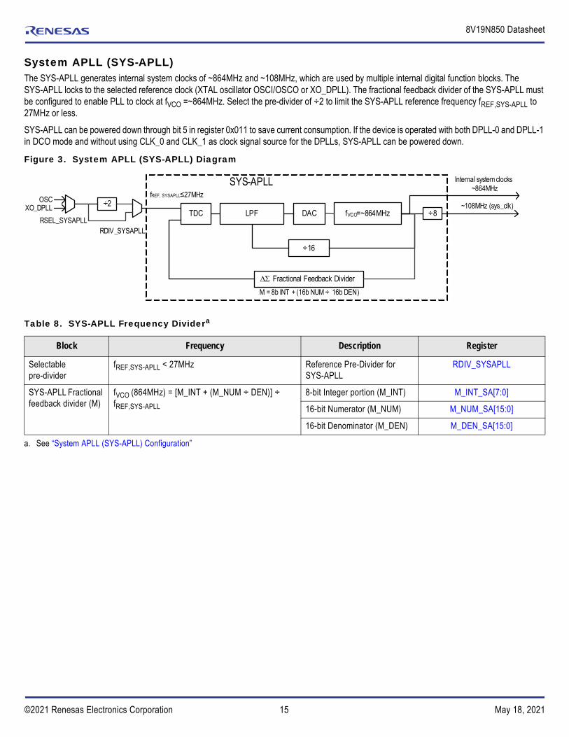
System APLL (SYS-APLL)The SYS-APLL generates internal system clocks of ~864MHz and ~108MHz, which are used by multiple internal digital function blocks. The SYS-APLL locks to the selected reference clock (XTAL oscillator OSCI/OSCO or XO_DPLL). The fractional feedback divider of the SYS-APLL must be configured to enable PLL to clock at fVCO =~864MHz. Select the pre-divider of ÷2 to limit the SYS-APLL reference frequency fREF,SYS-APLL to 27MHz or less.
SYS-APLL can be powered down through bit 5 in register 0x011 to save current consumption. If the device is operated with both DPLL-0 and DPLL-1 in DCO mode and without using CLK_0 and CLK_1 as clock signal source for the DPLLs, SYS-APLL can be powered down.
Figure 3. System APLL (SYS-APLL) Diagram
Table 8. SYS-APLL Frequency Dividera
a. See “System APLL (SYS-APLL) Configuration”
Block Frequency Description Register
Selectable pre-divider
fREF,SYS-APLL < 27MHz Reference Pre-Divider for SYS-APLL
RDIV_SYSAPLL
SYS-APLL Fractional feedback divider (M)
fVCO (864MHz) = [M_INT + (M_NUM ÷ DEN)] ÷ fREF,SYS-APLL
8-bit Integer portion (M_INT) M_INT_SA[7:0]
16-bit Numerator (M_NUM) M_NUM_SA[15:0]
16-bit Denominator (M_DEN) M_DEN_SA[15:0]
Internal system clocks~864MHz
fVCO=~864MHz
÷16
LPF
Fractional Feedback Divider
M = 8b INT + (16b NUM ÷ 16b DEN)
SYS-APLL
OSCXO_DPLL
÷8÷2
DACTDC
fREF, SYSAPLL ≤27MHz
~108MHz (sys_clk)
RSEL_SYSAPLLRDIV_SYSAPLL

16©2021 Renesas Electronics Corporation May 18, 2021
8V19N850 Datasheet
System DPLL (SYS-DPLL)The use of the SYS-DPLL is optional. When used, the purpose of the SYS-DPLL is to generate an internal frequency that is used for combo mode. The SYS-DPLL locks to an external oscillator on XO_DPLL (XO, TCXO, or OCXO) as a frequency reference for the device. By using the SYS-DPLL as a combo master with DPLL-0 or DPLL-1 as slave DPLLs, DPLL-0 and DPLL-1 will have the same frequency stability of the external oscillator locked to the SYS-DPLL. SYS-DPLL can only be used as a master for the combo bus.
When using SYS-DPLL, it is recommended to also have SYS-APLL locked the XO_DPLL so that the reference monitors have the same frequency stability of the external oscillator.
The SYS-DPLL implementation uses the APLL-2 as a high-speed oscillator. Therefore, APLL-2 is not available to be used as stand-alone synthesizer when the SYS-DPLL is used. When using the SYS-DPLL together with APLL-2, DPLL-0 must be also powered on.
Figure 4. System DPLL (SYS-DPLL) Diagram
Table 9. SYS-DPLL Frequency Dividera in SYS-DPLL Mode (SYNTH_MODE = 0)
a. See System DPLL (SYS-DPLL) Configuration and APLL-2.
Block Frequencyb
b. fxo is the OSCI/OSCO/XO_DPLL frequency.
Description Register
SYS-DPLL Fractional feedback divider (FFB)
fVCO-2 = ½ fTCXO [M_INT_SD + (M_NUM_SD ÷ M_DEN_SD)]
10-bit Integer portion (M_INT) M_INT_SD[9:0]
16-bit Numerator (N_NUM) M_NUM_SD[15:0]
16-bit Denominator (M_DEN) M_DEN_SD[15:0]
APLL-2 Fractional feedback divider
fVCO_2 = 2 fXO [M_INT + (M_NUM ÷ M_DEN)] 8-bit Integer portion M_INT_APLL2[7:0]
24-bit Numerator M_NUM_APLL2[23:0]
24-bit Denominator M_DEN_APLL2[23:0]
fVCO = 3600‐3868 MHz

17©2021 Renesas Electronics Corporation May 18, 2021
8V19N850 Datasheet
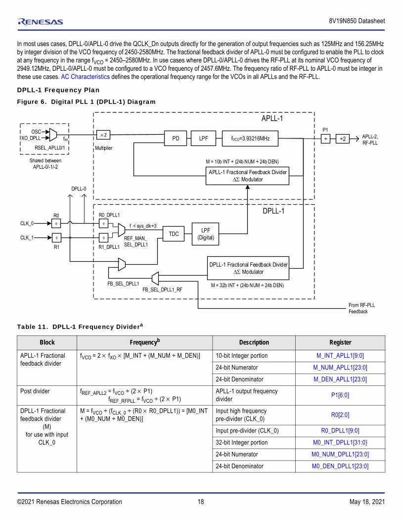
Digital PLLs (DPLL-0, DPLL-1)DPLL-0 Frequency Plan
Figure 5. Digital PLL 0 (DPLL-0) Diagram
Table 10. DPLL-0 Frequency Dividera
a. See DPLL-0 (APLL-0) Frequency Configuration and DPLL-0 Fractional Feedback Divider M1.
Block Frequencyb
b. fxo is the OSCI/OSCO/XO_DPLL frequency
Description Register
APLL-0 Fractional feedback divider
fVCO = 2 fXO [M_INT + (M_NUM ÷ M_DEN)] 10-bit Integer portion M_INT_APLL0[9:0]
24-bit Numerator M_NUM_APLL0[23:0]
24-bit Denominator M_DEN_APLL0[23:0]
Post divider P0 fREF_APLL2 = fVCO ÷ (2 P0)fREF_RFPLL = fVCO ÷ (2 P0)
APLL-0 output frequency divider P0[6:0]
DPLL-0 Fractional feedback divider
(M)for use with input
CLK_0
M = fVCO ÷ (fCLK_0 ÷ (R0 R0_DPLL0)) = [M0_INT + (M0_NUM ÷ M0_DEN)]
Input high frequency pre-divider (CLK_0)
R0[2:0]
Input pre-divider (CLK_0) R0_DPLL0[9:0]
32-bit Integer portion M0_INT_DPLL0[31:0]
24-bit Numerator M0_NUM_DPLL0[23:0]
24-bit Denominator M0_DEN_DPLL0[23:0]
DPLL-0 Fractional feedback divider
(M)for use with input
CLK_1
M = fVCO ÷ (fCLK_1 ÷ (R1R1_DPLL0)) = [M1_INT + (M1_NUM ÷ M1_DEN)]
Input high frequency pre-divider (CLK_1)
R1[2:0]
Input pre-divider (CLK_1) R1_DPLL0[9:0]
32-bit Integer portion M1_INT_DPLL0[31:0]
24-bit Numerator M1_NUM_DPLL0[23:0]
24-bit Denominator M1_DEN_DPLL0[23:0]
18©2021 Renesas Electronics Corporation May 18, 2021
8V19N850 Datasheet
In most uses cases, DPLL-0/APLL-0 drive the QCLK_Dn outputs directly for the generation of output frequencies such as 125MHz and 156.25MHz by integer division of the VCO frequency of 2450-2580MHz. The fractional feedback divider of APLL-0 must be configured to enable the PLL to clock at any frequency in the range fVCO = 2450–2580MHz. In use cases where DPLL-0/APLL-0 drives the RF-PLL at its nominal VCO frequency of 2949.12MHz, DPLL-0/APLL-0 must be configured to a VCO frequency of 2457.6MHz. The frequency ratio of RF-PLL to APLL-0 must be integer in these use cases. AC Characteristics defines the operational frequency range for the VCOs in all APLLs and the RF-PLL.
DPLL-1 Frequency Plan
Figure 6. Digital PLL 1 (DPLL-1) Diagram
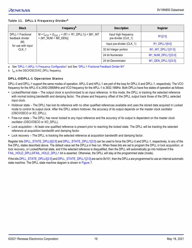
Table 11. DPLL-1 Frequency Dividera
Block Frequencyb Description Register
APLL-1 Fractional feedback divider
fVCO = 2 fXO [M_INT + (M_NUM ÷ M_DEN)] 10-bit Integer portion M_INT_APLL1[9:0]
24-bit Numerator M_NUM_APLL1[23:0]
24-bit Denominator M_DEN_APLL1[23:0]
Post divider fREF_APLL2 = fVCO ÷ (2 P1)fREF_RFPLL = fVCO ÷ (2 P1)
APLL-1 output frequency divider
P1[6:0]
DPLL-1 Fractional feedback divider
(M)for use with input
CLK_0
M = fVCO ÷ (fCLK_0 ÷ (R0 R0_DPLL1)) = [M0_INT + (M0_NUM ÷ M0_DEN)]
Input high frequency pre-divider (CLK_0)
R0[2:0]
Input pre-divider (CLK_0) R0_DPLL1[9:0]
32-bit Integer portion M0_INT_DPLL1[31:0
24-bit Numerator M0_NUM_DPLL1[23:0]
24-bit Denominator M0_DEN_DPLL1[23:0]
fVCO=3.93216MHz
APLL-1 Fractional Feedback DividerModulator
LPF(Digital)
TDC
PD LPF
DPLL-1 Fractional Feedback DividerModulator
M = 10b INT + (24b NUM ÷ 24b DEN)
M = 32b INT + (24b NUM ÷ 24b DEN)
APLL-1
R0
CLK_0 ÷
R1
CLK_1 ÷
÷ ÷2
P1
f < sys_clk÷3
2
Multiplier
APLL-2,RF-PLL
DPLL-0
DPLL-1
÷
÷
R0_DPLL1
R1_DPLL1
REF_MAN_SEL_DPLL1
FB_SEL_DPLL1
OSCXO_DPLL fX0
RSEL_APLL0/1
Shared between APLL-0/-1/-2
FB_SEL_DPLL1_RF
From RF-PLL Feedback
19©2021 Renesas Electronics Corporation May 18, 2021
8V19N850 Datasheet
DPLL-0/DPLL-1 Operation StatesDPLL-0 and DPLL-1 support the same modes of operation. APLL-0 and APLL-1 are part of the loop for DPLL-0 and DPLL-1, respectively. The VCO frequency for the APLL-0 is 2450-2580MHz and VCO frequency for the APLL-1 is 3932.16MHz. Both DPLLs have five states of operation as follows: Locked/Normal state – The output clock is synchronized to an input reference. In this mode, the DPLL is tracking the selected reference
with normal locking bandwidth and damping factor. The phase and frequency offset of the DPLL output track those of the DPLL selected input clock.
Holdover state – The DPLL has lost its reference with no other qualified references available and uses the stored data acquired in Locked mode to control its output clock. After the DPLL enters holdover, the accuracy of its output depends on the master clock oscillator (OSCI/OSCO or XO_DPLL).
Free-run state – The DPLL has never locked to any input reference and the accuracy of its output is dependent on the master clock oscillator (OSCI/OSCO or XO_DPLL).
Lock acquisition – At least one qualified reference is present prior to reaching the locked state. The DPLL will be tracking the selected reference at acquisition bandwidth and damping factor.
Lock recovery – The DPLL is tracking the selected reference at acquisition bandwidth and damping factor.
Register bits DPLL_STATE_DPLL0[2:0] and DPLL_STATE_DPLL1[2:0] can be used to force the DPLL-0 and DPLL-1, respectively, to any of the five DPLL states described above. The default value set the DPLLs in free run. When these bits are set to program the DPLL in lock acquisition, or lock recovery, or Locked/Normal state, and if the selected reference is disqualified, then the DPLL will automatically go into holdover if the FAIL_HOLD_DPLL0/FAIL_HOLD_DPLL1 bit is asserted. Otherwise, the DPLL will stay at the programmed state (mode).
If the bits DPLL_STATE_DPLL0[2:0] and DPLL_STATE_DPLL1[2:0] are set to 0b101, then the DPLLs are programmed to use an internal automatic state machine. The DPLL state machine diagram is shown in Figure 7.
DPLL-1 Fractional feedback divider
(M)for use with input
CLK_1
M = fVCO ÷ (fCLK_1 ÷ (R1 R1_DPLL1)) = [M1_INT + (M1_NUM ÷ M0_DEN)]
Input high frequency pre-divider (CLK_1)
R1[2:0]
Input pre-divider (CLK_1) R1_DPLL1[9:0]
32 bit Integer portion M1_INT_DPLL1[31:0]
24 bit Numerator M1_NUM_DPLL1[23:0]
24 bit Denominator M1_DEN_DPLL1[23:0]
a. See “DPLL-1 (APLL-1) Frequency Configuration” and See “DPLL-1 Fractional Feedback Divider M1”b. fxo is the OSCI/OSCO/XO_DPLL frequency.
Table 11. DPLL-1 Frequency Dividera
Block Frequencyb Description Register

20©2021 Renesas Electronics Corporation May 18, 2021
8V19N850 Datasheet
Figure 7. DPLL State Machine Diagram
As showed in Figure 7, the DPLL state changes are as follows:1. After reset, the DPLL enters Free-Run State.
2. After an input clock is qualified and it is selected, it enters the Lock Acquisition State.
3. If the DPLL selected input clock is disqualified AND no qualified input clock is available, it goes back to Free-run State.
4. If the DPLL locks to the selected input clock, it enters Normal_lock State.
5. The DPLL selected input clock is disqualified AND No qualified input clock is available, it enters Holdover State.
6. If a qualified input clock is now available, it enters lock recovery State.
7. If the DPLL selected input clock is disqualified AND no qualified input clock is available, it goes back to Holdover State.
8. If the DPLL locks to the selected input clock, it enters Normal_lock State.
In state changes 6 above, the DPLL switches to another qualified clock because of one of the following: The selected input clock was disqualified and another qualified input clock is available
The device is set to revertive mode and a qualified input clock with a higher priority is available.
While in the Normal_lock state, if the input clock exceeds the programmed Lock Threshold, then the DPLL will enter the Holdover state.
Freerun
Lock Acquisition
Holdover
Normal_lock
Lock Recovery
No qualified ref
21©2021 Renesas Electronics Corporation May 18, 2021
8V19N850 Datasheet
DPLL Loop Bandwidth
The bandwidth (BW) of the DPLL is precise and static and independent on the clock frequency. The bandwidth of the DPLL does not change with the frequency plan. The bandwidth is programmable from 1mHz to approximately 6kHz.
There are two register fields associated with the bandwidth settings: NORMAL_BW_SHIFT_DPLL0[4:0]/ NORMAL_BW_SHIFT_DPLL1[4:0] and NORMAL_BW_MULT_DPLL0[2:0]/NORMAL_BW_MULT_DPLL1[2:0]. To calculate the BW, the following equation is used:
BW = (KTDC KPEC KP) / 2π
Where:KTDC = 1 / TDC_STEP
TDC_STEP = TSYSAPLL_VCO / 62 =18.67psKPEC = 2107 KP = (NORMAL_BW_SHIFT_DPLL0[4:0] /4) 2^(NORMAL_BW_MULT_DPLL0[2:0]-53)
Holdover StateIn holdover state, the DPLL has lost its reference and uses the stored data acquired in Locked mode to control its output clock. The initial frequency offset is 1.1 × 10⁻⁷ppb. After the DPLL enters holdover, the accuracy of its output depends on the master clock oscillator (connected to OSCI/OSCO or XO_DPLL/nXO_DPLL pins). If the SYS-DPLL is enabled, then it is assumed that the SYS-DPLL is locked to the master clock oscillator that is connected to XO_DPLL/nXO_DPLL pins, and therefore the holdover is based on this master clock oscillator. If SYS-DPLL is not enabled, then holdover is based on the master clock oscillator that is connected to the OSCI/OSCO pins.
The 8V19N850 supports the following holdover states: Instantaneous Holdover
History Instantaneous Holdover
History Averaged Holdover
Manual Holdover
The holdover states can be set by programming bits HOLDOVER_MODE_DPLL0[1:0] and HOLDOVER_MODE_DPLL1[1:0] for DPLL-0 and DPLL-1, respectively.
Instantaneous Holdover
If DPLL-0/-1 is set to operate in Instantaneous Holdover, then the DPLL freezes at the operating frequency when it enters holdover state. The initial frequency offset is better than is 1.1 × 10⁻⁷pbb assuming that there is no in-band jitter/wander at the input just before entering holdover state.
History Instantaneous Holdover
The 8V19N850 implements a history of the instantaneous holdover values. Previously stored instantaneous holdover value can be retrieved. The rate at which the holdover registers are stored is programmable. It can be programmed in steps of 1 second between 1 and 64 s by programming register bits, HOLDOVER_HISTORY_DPLL0[5:0] and HOLDOVER_MODE_DPLL1[1:0] for DPLL-0 and DPLL-1 respectively. The default value is 1s.
History Averaged Holdover
When a DPLL is set to history averaged holdover state, the holdover value is post filtered. The filter bandwidth is programmable from approximately 0.12mHz to 0.5Hz. When a DPLL enters the history averaged holdover state, the holdover register value is restored into the integrator inside that DPLL. The rate at which the holdover registers are stored is programmable between 1 and 64 s in steps of 1 s by programming register bits HOLDOVER_HISTORY_DPLL0[5:0] and HOLDOVER_HISTORY_DPLL1[5:0] for DPLL-0 and DPLL-1, respectively. The default value is 1s.
The holdover filter bandwidth value is programmed by setting HOLDOVER_BW_SHIFT_DPLL0[4:0] / HOLDOVER_BW_SHIFT_DPLL1[4:0] (for DPLL-0) and HOLDOVER_MULT_DPLL1[2:0] / HOLDOVER_MULT_DPLL1[2:0] (for DPLL-1) as follows:
Holdover filter bandwidth = coe f / (2π) where coe = 2-(33-HOLDOVER_BW_SHIFT_DPLLn) HOLDOVER_MULT_DPLLn / 4 (n = 0 for DPLL-0, n = 1 for DPLL-1)
f is the update rate of both DPLLs (600kHz).
If coe is zero then the filter is bypassed.

22©2021 Renesas Electronics Corporation May 18, 2021
8V19N850 Datasheet
Manual Holdover
In manual holdover, the frequency offset is set by the DPLL manual holdover value register bits HOLDOVER_VALUE_DPLL0[41:0] and HOLDOVER_VALUE_DPLL1[41:0] for DPLL-0 and DPLL-1, respectively.
Forced into Holdover
The DPLL can also be forced into the holdover state. If it is forced into holdover state, then the DPLL will stay in holdover even if there are valid references available for the DPLL to lock to. Register bits DPLL_STATE_DPLL0[2:0] and DPLL_STATE_DPLL1[2:0] can be used to set the DPLL-0 and DPLL-1, respectively, to holdover.
Pull-in/Hold-inBoth DPLLs support independently a pull-in range of ±4.6 × 10⁻⁶, ±12 × 10-6, ±20 × 10-6, ±32 × 10-6, ±52 × 10-6, ±83 × 10-6, ±131 × 10-6, and ±147 × 10-6.
Free-Run Frequency Accuracy
The free-run accuracy is dependent on the oscillator, both DPLLs support free run accuracy based on the local oscillator.
Phase Slope Limiting (PSL)Each DPLL supports independent phase slope limiting that is programmable through registers. Each DPLL allows the phase slope limiting to be set such as 1ns/s, 5ns/s, 10 ns/s, 885ns/s, 7.5s/s, or 61s/s to meet different applications. It can also be bypassed.
IEEE 1588 Modes of operation
Write Frequency Mode
The DCO circuits from DPLL-0 and DPLL-1 can be controlled by a digital word that can represent phase offset and frequency offset. Bits WRITE_FREQUENCY_EN_DPLL0 and WRITE_FREQUENCY_EN_DPLL1can be used to program DPLL-0 and DPLL-1 respectively in the write frequency mode.
Figure 8 shows the DCO being controlled by writing a frequency control word into the DCO. The Frequency Control Word (FCW) is used to adjust the frequency output of the DCO, the phase detector and loop filter are bypassed. In this case, the filtering is done by an external processor that will be controlling the DCO. The frequency offset written into the register is passed on directly to the output clocks. The FCW (WRITE_FREQUENCY_DPLL0[41:0]/WRITE_FREQUENCY_DPLL1[41:0]) is a 42-bit 2’s-complement value, the total range is ±244ppm of the nominal DCO frequency, and the DCO programming resolution is 1.1 × 10⁻⁷ppb.
Figure 8. Write Frequency Mode
TDCREF LPF
DPLL
PD VCOLPF
fcw DCO
write_phase
write_frequency
syscombo fcw from SYSDPLL (48‐b)
combo fcw from another DPLL (48‐b)
x2
OSC
XO_DPLL
phase_offset
APLL-0 Fractional Feedback DividerModulator
DPLL-x Fractional Feedback DividerModulator

23©2021 Renesas Electronics Corporation May 18, 2021
8V19N850 Datasheet
In write frequency mode, APLL VCO is tuned by the FCW as follows:
fvco = fxoN(1+FCW)
Where:fvco is the APLL VCO frequency.fxo is the OSCI/OSCO/XO_DPLL frequency which is fixed.N is the nominal APLL feedback divider ratio.FCW is the tuning word which is 42-bit 2's complement and LSB is 2-53.FCW is calculated as follows:FCW = FFO10-6 253
andFFO is the target fractional frequency in ppm.
As an example, change the output frequency by 10ppb (10 10-3ppm) on DPLL-1:
Control word (in decimal): 1010-3 10-6 253 = 90,071,992.547409020
Convert 90,071,992 into Hex (0x55E63B8) to write into register (WRITE_FREQUENCY_DPLL0[41:0]/WRITE_FREQUENCY_DPLL1[41:0]).
Write Phase Mode
Each DCO of DPLL-0 and DPLL-1 can be controlled by a digital word that can represent phase offset, and use the hardware loop filter to filter it per Figure 9.
Bits WRITE_PHASE_EN_DPLL0 and WRITE_PHASE_EN_DPLL1 can be used to program DPLL-0 and DPLL-1 respectively in the write phase mode.
Figure 9. Write Phase Mode
Figure 9 shows the DCO being controlled by writing a phase offset word into the DCO, then an external processor directly controls the DCO phase through the Microport interface with hardware controlled bandwidth (e.g., 0.1Hz per G.8273.2) and phase slope limiting.
The phase control word (PCW) can be written into WRITE_PHASE_DPLL0[31:0]/WRITE_PHASE_DPLL1[31:0] bits for DPLL-0/1.
The PCW is a 32-bit 2’s-complement value. The resolution of the PCW is 1 TDC step. The TDC step is TSYSAPLL_VCO / 62 and the range is ±(2147483647(TDC step)). For example, if the system DPLL VCO frequency is 864MHz, then the TDC step is 18.6678614097969ps, and the range is ±40.0889271020012ms.
TDCREF LPF
DPLL
PD VCOLPF
fcw
DPLL-x Fractional Feedback DividerModulator
DCO
write_phase
write_frequency
syscombo fcw from SYSDPLL (48‐b)
combo fcw from another DPLL (48‐b)
x2
OSC
XO_DPLL
phase_offset
APLL-0 Fractional Feedback DividerModulator
24©2021 Renesas Electronics Corporation May 18, 2021
8V19N850 Datasheet
The PCW applied to LPF (Low Pass Filter) is equivalent to applying a phase error measured by the on-chip TDC (Phase Detector) applied to LPF when the DPLL is operating in closed loop. The update rate needs to be at least 60 times of the loop filter bandwidth; as an example, for 0.1Hz, the update rate should be greater than 6Hz.
To assist in the above, there is an optional timer associated with the PCW and the FCW. This allows a phase/frequency control word to be applied for a limited period of time after which it will automatically go into holdover, and therefore it will avoid the DCO to continue to apply the phase/frequency adjustment indefinitely until it reaches its tuning range limits. The timer value is a 16-bit integer (see WRITE_TIMER_DPLL0[15:0]/WRITE_TIMER_DPLL1[15:0]), it can be set in multiples of 125s.
Combo Mode
The 8V19N850 supports DPLL combo mode. Both DPLL-0 or DPLL-1 can be programmed to either the combo master (the generator of the frequency control word (FCW), or the combo slave (the receiver of the FCW).
For example, if COMBO_MODE_EN_DPLL0 is set to zero, and COMBO_MODE_EN_DPLL1 is set to 1, then DPLL-0 is the combo master and DPLL-1 is the combo slave. In this example, DPLL-0 can be locked to an input reference clock, such as a Synchronous Ethernet clock, which is a regular PLL channel and can generate output clocks of different frequencies that track the Synchronous Ethernet input reference clock. And the DPLL-1 can be used as a DCO and it will be controlled externally, as an example by an IEEE 1588 clock recovery servo algorithm running in an external processor.
In this example, the IEEE 1588 timestamps can be used to calculate the phase offset between the IEEE 1588 master’s 1PPS pulse and the IEEE 1588 slave’s 1PPS pulse and then align the two pulses by moving the slave’s 1PPS pulse in phase. The phase offset between the IEEE 1588 master’s 1PPS pulse and the IEEE 1588 slave’s 1PPS pulse can be written into the Phase Control Word into DPLL-1 channel over the serial port to correct the phase, as described in the Write-Phase Mode section.
Figure 10 shows a functional block diagram of the combo mode.

25©2021 Renesas Electronics Corporation May 18, 2021
8V19N850 Datasheet
Figure 10. Combo Mode Functional Block Diagram
The phase and frequency offsets between the combo master and slave are available for software to read at all times. The frequency information can be temporarily placed on hold (i.e., to ride out a phase transient).
TDCREF DLPF
APLL‐0
fcw
DPLL-1 Fractional Feedback DividerModulator
write_phase
write_frequency
syscombo from SYSDPLL (48‐b)
combo from other DPLL (48‐b)
phase _offset
TDCREF DLPF
DPLL‐1APLL‐1
fcw
write_phasewrite_frequency
syscombo fcw from SYSDPLL (48‐b)
combo fcw from other DPLL (48‐b)
phase_offset
DPLL-0 Fractional Feedback DividerModulator
DPLL‐0

26©2021 Renesas Electronics Corporation May 18, 2021
8V19N850 Datasheet
Phase Adjustment through DPLL
The 8V19N850 supports phase adjustments to be done through the DPLL-0 and DPLL-1. Figure 11 shows a functional block DPLL-0/-1.
Figure 11. DPLL-0/-1 Functional Block Diagram
When DPLL-0/-1 is locked to a clock, the phase of the output clock can be adjusted using a Phase Offset Word (phase_offset in Figure 11).
The phase offset word (POW) is a 36-bit 2’s-complement value. It can be written into PHASE_OFFSET_DPLL0[35:0]/PHASE_OFFSET_DPLL1[35:0] bits for DPLL-0/1. The resolution of the POW is 1 TDC step. The TDC step is TSYSAPLL_VCO / 62 and the range is ±(2147483647(TDC_STEP)). For example, if the system DPLL VCO frequency is 864MHz, then the TDC step is 18.6678614097969ps, and the range is ±40.0889271020012ms.
Input Clock Qualification and Reference Selection
The input clock qualification is based on the reference monitoring (for more information, see Input Clock Quality Monitoring). The device has three reference selection modes set by the REF_SEL_MODE_DPLL0/1 bits as follows: Pin selection mode through selection pins (assigned GPIO pins)
Manual selection mode through register bits set through SPI/I3C interface.
Automatic input clock selection mode
There is an independent reference selection process for each DPLL. The mode for each DPLL can be set as shown in Table 12
Table 12. REF_SEL_MODE_DPLL0/1 Bits to Select the DPLL Mode
REF_SEL_MODE_DPLL0[1:0],REF_SEL_MODE_DPLL1[1:0] Description
00 Pin Selection Mode through assigned GPIO pins
01 Manual selection Mode through register bits set through SPI/I3C interface
10 Automatic selection mode
11 Reserved
TDCREF DLPF
APLL‐0/‐1
fcw
DPLL-1 Fractional Feedback DividerModulator
write_phase
write_frequency
syscombo from SYSDPLL (48‐b)
combo from other DPLL (48‐b)
phase _offset
DPLL‐0/‐1
27©2021 Renesas Electronics Corporation May 18, 2021
8V19N850 Datasheet
Pin Selection Mode
In this mode, if REF_SEL_MODE_DPLL0/1[1:0] are set to 00, then both DPLLs lock to the input reference selected by GPIOs
The input clock monitoring will continue to monitor the input clock, and if the selected input reference fails and the bit fail_hold is set, then the DPLL will enter holdover automatically. The DPLL will automatically recover from holdover (or free-run) when the reference becomes valid or if another valid reference is selected by GPIO (CLKnSEL1/0) pins. If the selected reference is invalid and no other valid reference gets selected by the GPIO (CLKnSEL1/0) pins, then the DPLL will continue in holdover state.
If fail_hold bit is not set, then the DPLL continues to lock to the reference clock selected by GPIO (CLKnSEL1/0) pins, even if that particular reference is no longer valid. The DPLL will continue to track the clock selected by GPIO (CLKnSEL1/0) pins and will do a reference switching once the GPIO (CLKnSEL1/0) pins select another clock input. If the selected reference is invalid and no other valid reference gets selected by the GPIO (CLKnSEL1/0) pins, then the DPLL will continue to track to the invalid reference.
In this mode, when doing a reference switching between two inputs, they must be at the same frequency. If they have different frequencies, then the input dividers can be used to divide down the frequency to a common frequency to the internal input of the DPLL.
Manual Selection Mode
In this mode, each DPLL locks to the input reference selected by ref_man_sel_dpll0/1 bit in the appropriated register per Table 15.
In this mode, each DPLL has its own set of registers and therefore each DPLL can select a different input based on the ref_man_sel_dpll0/1 selection bits for each DPLL. The automatic state machine is disabled and the input clock monitoring does not affect the input clock selection.
In this mode, the input clock selection is done by setting the proper bits in the control registers related to each DPLL, the input clock monitoring will continue to monitor the input clock (see Input Clock Quality Monitoring), and if the selected input reference fails, then the DPLL will enter holdover automatically. The DPLL will automatically recover from holdover (or free-run) when the reference becomes valid or if another valid reference is selected by the ref_man_sel_dpll0/1 register bit.
In this mode, if the selected reference is invalid and no other valid reference gets selected by the ref_man_sel_dpll0/1 register bit, then the DPLL will enter holdover state.
Table 13. Reference Input Selection by Pins for DPLL-0
Selection by GPIOCLKnSEL0 Description
0 CLK_0
1 CLK_1
Table 14. Reference Input Selection by Pins for DPLL-1
Selection by GPIOCLKnSEL1 Description
0 CLK_0
1 CLK_1
Table 15. Manual Reference Input Selection by Register Bits
ref_man_sel_dpll0/1 Description
0 CLK_0
1 CLK_1

28©2021 Renesas Electronics Corporation May 18, 2021
8V19N850 Datasheet
Automatic Input Clock Selection Mode
If automatic input clock selection is used, then an internal automatic state machine will automatically do reference switching and the input clock selection is determined by the input clock being qualified. An input is considered qualified based on being valid by the clock monitor (see Input Clock Quality Monitoring), the priority of each input clock, and the input clock configuration.
If bits DIS_CLK0_BY_PIN and DIS_CLK1_BY_PIN are set to 1, then a GPIO (see Input Disqualification by GPIO pins) can be used to disable CLK_0 and CLK_1 to be used by DPLL-O and DPLL-1.
If bits DIS_CLK0_BY_PIN and DIS_CLK1_BY_PIN are set to 0, then bits DIS_CLK0 and DIS_CLK1 can be used to disable CLK_0 and CLK_1 to be used by DPLL-O and DPLL-1. If the input is enabled (DIS_CLK0 or DIS_CLK1 is set to 0) and the reference monitors declare that input valid, then that input is qualified to be used by the DPLLs. If the input is disabled (DIS_CLK0 or DIS_CLK1 is set to 1), and even though the reference monitors declare that input valid, then that input is disqualified to be used by the DPLLs.
Within all the qualified inputs, the one with the highest priority is selected by the DPLL. The input clock priority is set by setting bits REF_PRIORITY_DPLL0 and REF_PRIORITY_DPLL1 for DPLL-0 and DPLL-1 respectively.
Reference Switching
Automatic reference Switching
In Automatic Locked Mode, the input clock selection must be determined by the input clock being qualified. An input is considered qualified based on being valid by the clock monitor (see Input Clock Quality Monitoring), the priority of each input clock, and the input clock configuration.
The input clock must be declared valid depending on the results of input clock quality monitoring (refer to Input Clock Quality Monitoring). Within all the valid input clocks (the ones that do not have fail alarm(s)), the one with the highest priority must be selected.
The priority must be set by setting bits REF_PRIORITY_DPLL0 and REF_PRIORITY_DPLL1 for DPLL-0 and DPLL-1 respectively. The input clock must also be configured to be valid or invalid by register configuration. If hitless reference switching is enabled, then the output phase change is below 1ns when the device performs a reference switching between two reference inputs that are integer multiple ratios of each other, and are divided down to the least common frequency through the pre-dividers.
Hitless Reference Switching
Hitless reference switching is supported for all frequency clocks.
The Hitless Switching (HS) circuit eliminates phase transients on the output clock that may occur during reference switching or the recovery from Holdover state to Locked state. On recovery from holdover state or when switching to another reference input, the HS circuit measures the phase delay between the current phase (feedback signal) and the phase of the newly selected reference input. This delay value is used by the PLL to minimize the phase transient it experiences when it switches to another reference input or recovers from holdover state.
An HS event must be triggered if either of the following conditions occurs: DPLLs selected input clock switches to a different reference
DPLLs exits from holdover state
For the two conditions above, the phase transients on the DPLLs output are minimized < 1ns with Hitless Switching (HS) enabled.
If HS is disabled, then there may be a phase shift on the DPLLs output, as the DPLLs output tracks back to 0 degree phase offset with respect to the DPLLs selected input clock.
When HS is enabled, there could be cases where it is needed to clear the phase (as an example, the DPLL goes into holdover for a long period of time, and therefore it is better to not do a hitless reference switching when it recovers from a long-term holdover state). In this case a bit, HS_CLR, can be set to clear the delay value (TIE). In general, HS_CLK should not be exercised when holdover state is entered for short time periods. The speed of the phase alignment correction is limited by the PSL setting.
29©2021 Renesas Electronics Corporation May 18, 2021
8V19N850 Datasheet
Revertive and Non-Revertive Reference Switching
The 8V19N850 supports revertive and non-revertive reference switching. Revertive switching can be disabled by register bit.
Input Clock Quality Monitoring
The quality of all the input reference clocks is always monitored individually (excluding the OSCI/OSCO or XO_DPLL input), 8V19N850 has 3 reference monitors as follows: Short-term monitor (this monitor can be used for LOS (loss of signal) detector)
Medium-term monitor (this monitor can be used for activity)
Long-term monitor (this monitor can be used for detecting frequency offset)
Each input clock can be individually configured for monitoring, and each monitor type can be masked. The active reference is also monitored to ensure that it is still a valid reference. If an input clock fails, then an alarm will be generated, an input clock with an alarm condition cannot be used for an input reference if the alarm is not masked. The reference monitor is based on reference clock of the system APLL (OSCI/OSCO or XO_DPLL). A TCXO/OCXO must be used for better accuracy.
Short-Term Monitor
Each input clock reference is monitored using the short-term monitor.The short-term monitor can be used to detect loss of signal. It supports input clock frequencies equal to or above 1MHz.
The short-term monitor takes the input clock from after the input high frequency pre-divider (maximum frequency is 36MHz) and before the input pre-divider. The period of this frequency is used to create a window to compare whether or not the input clock is within a certain frequency. The window size is programmable. Window size = TREF (if DIV_RATIO_ST is set to 0 or to 1)
Window size = (DIV_RATIO_ST+2) TREF
TREF = period of the input reference clock, after high frequency pre-divider
Where DIV_RATIO_ST is programmable by using bits DIV_RATIO_ST_REF_MON0[5:0] and DIV_RATIO_ST_REF_MON1[5:0] for CLK_0 and CLK_1, respectively.
A counter that is part of the short-term monitor is used to count the number of system clocks (SYS_CLK that is approximately 108MHz) within the window.
The nominal counter value is calculated as follows: NOMINAL_NUM_ST = fSYS_CLK / fREF (if DIV_RATIO_ST is set to 0 or to 1)
NOMINAL_NUM_ST = fSYS_CLK / (fREF / (DIV_RATIO_ST + 2))
fSYS_CLK = ~108MHz
fREF = frequency of the input reference clock, after high frequency pre-divider
The NOMINAL_NUM_ST value is then set into NOMINAL_NUM_ST_REF_MON0[7:0] and NOMINAL_NUM_ST_REF_MON1[7:0] for CLK_0 and CLK_1 respectively.
There is a comparator that compares an internal counter with the nominal counter value. A hysteresis counter is used to avoid the monitor to flip back an forth on detecting a good/bad reference when it is on the edge. There is an acceptance range and a rejection range that are also programmable.
The acceptance range to be added to the nominal counter value is programmable by setting bits ACCEPT_NUM_ST_REF_MON0[3:0] and ACCEPT_NUM_ST_REF_MON1[3:0] for CLK_0 and CLK_1 respectively.
The rejection range to be added to the nominal counter value is programmable by setting bits REJECT_NUM_ST_REF_MON0[3:0] and REJECT_NUM_ST_REF_MON1[3:0] for CLK_0 and CLK_1 respectively.
There is a counter that counts the number of times the reference is declared good by the short-term reference monitor. This counter is programmable by setting its GOOD_TIMES_ST_REF_MON0[3:0] and GOOD_TIMES_ST_REF_MON1[3:0] for CLK_0 and CLK_1 respectively. This counter is used to clear the fail status bits after the reference has been detect to be good by the number of times set in this register.

30©2021 Renesas Electronics Corporation May 18, 2021
8V19N850 Datasheet
There is a counter that counts the number of times the reference is declared invalid by the short-term reference monitor. This counter is programmable by setting its FAIL_NUM_ST_REF_MON0[3:0] and FAIL_NUM_ST_REF_MON1[3:0] for CLK_0 and CLK_1 respectively. This counter is used to set the fail status bits after the reference has been detect to be bad by the number of times set in this register.
Short-term monitor has a bit associated with it to mask the failure alarm. It also has a bit to mask the interrupt generation. Short-term monitor generates an interrupt if not masked by the associate interrupt mask bit.
It is recommended to always set the acceptance range of the internal counter to be greater than 3, and the rejection number greater than the acceptance range. It is also recommended to set the GOOD_TIMES_ST_REF_MON0/1 greater than the FAIL_NUM_ST_REF_MON0/1 to disqualify the reference quicker. The default value for GOOD_TIMES_ST_REF_MON0/1 is 4 and the default value for the FAIL_NUM_ST_REF_MON0/1 is 1.
As an example, to declare loss of signal on CLK_0 (1MHz) if one clock cycle is missing. The registers are preprogrammed as follows: DIV_RATIO_ST_REF_MON0[5:0] = 0 (Window size = 1s)
NOMINAL_NUM_ST_REF_MON0[7:0] = 108M/(1M) = 108
ACCEPT_NUM_ST_REF_MON0[3:0] = 5
REJECT_NUM_ST_REF_MON0[3:0] = 11
FAIL_NUM_ST_REF_MON0[3:0] = 1
GOOD_TIMES_ST_REF_MON0[3:0] = 2
In this example, the acceptance range of the internal counter is from 103 to 113 cycles, and the rejection range is below 98 or greater than 118 cycles. The CLK_0_FAIL_ST bit will be set after the short-term reference monitor detects one missing clock (FAIL_NUM_ST_REF_MON0[3:0] is set to 1), and it is back to normal after the reference monitor detects two good clock cycles (as GOOD_TIMES_ST_REF_MON0[3:0] = 2).
Figure 12. Short-Term Reference Monitor Example (CLK_0 is Missing One Clock Cycle)
Medium-Term Monitor
Each input clock reference is monitored using the medium-term monitor. The medium-term monitor can be used to detect activity with coarse resolution (i.e., PPM). It supports input clock frequencies above 1kHz.
The medium-term monitor takes the input clock after the input high frequency pre-divider (maximum frequency is 36MHz) and before the input pre-divider. The period of this frequency is used to create a window to compare whether or not the input clock is within a certain frequency. The window size is programmable. Window size = TREF (if DIV_RATIO_MT is set to 0 or to 1)
Window size = (DIV_RATIO_MT+2) TREF
TREF = period of the input reference clock, after high frequency pre-divider
Where DIV_RATIO_MT is programmable by using bits DIV_RATIO_MT_REF_MON0[15:0] and DIV_RATIO_MT_REF_MON1[15:0] for CLK_0 and CLK_1 respectively.
A counter that is part of the medium-term monitor is used to count the number of system clocks (SYS_CLK that is approximately 108MHz) within the window.
CLK_0 (missing one clock period)
Window
clk_sys(108MHz)
cycle_count=0Internal
counter value
CLK_0_FAIL_ST
0 1 2
Window size
117 118 214215 1
Window size
0 1 2 107106 1
Window size
0 1 2 107106 0119 120
Window size
10 1 2 107106 0

31©2021 Renesas Electronics Corporation May 18, 2021
8V19N850 Datasheet
The nominal counter value is calculated as follows: NOMINAL_NUM_MT = fSYS_CLK / fREF (if DIV_RATIO_MT is set to 0 or to 1)
NOMINAL_NUM_MT = fSYS_CLK / (fREF / (DIV_RATIO_MT + 2))
fSYS_CLK = ~108MHz
fREF = frequency of the input reference clock, after high frequency pre-divider
The NOMINAL_NUM_MT value is then set into NOMINAL_NUM_MT_REF_MON0[17:0] and NOMINAL_NUM_MT_REF_MON1[17:0] for CLK_0 and CLK_1 respectively.
There is a comparator that compares an internal counter with the nominal counter value. A hysteresis counter is used to avoid the monitor to flip back an forth on detecting a good/bad reference when it is on the edge. There is an acceptance range and a rejection range that are also programmable.
The acceptance range to be added to the nominal counter value is programmable by setting bits ACCEPT_NUM_MT_REF_MON0[15:0] and ACCEPT_NUM_MT_REF_MON1[15:0] for CLK_0 and CLK_1 respectively.
The rejection range to be added to the nominal counter value is programmable by setting bits REJECT_NUM_MT_REF_MON0[15:0] and REJECT_NUM_MT_REF_MON1[15:0] for CLK_0 and CLK_1 respectively.
There is a counter that counts the number of times the reference is declared good by the medium-term reference monitor. This counter is programmable by setting its GOOD_TIMES_MT_REF_MON0[3:0] and GOOD_TIMES_MT_REF_MON1[3:0] for CLK_0 and CLK_1 respectively. This counter is used to clear the fail status bits after the reference has been detect to be good by the number of times set in this register.
There is a counter that counts the number of times the reference is declared invalid by the medium-term reference monitor. This counter is programmable by setting its FAIL_NUM_MT_REF_MON0[3:0] and FAIL_NUM_MT_REF_MON1[3:0] for CLK_0 and CLK_1 respectively. This counter sets the fail status bits after the reference has been detected to be bad by the number of times set in this register.
If the internal counter value is within the nominal counter value ± the acceptance range, then the reference is considered good. If the internal counter value is outside the nominal counter value ± the rejection range, then the reference is considered bad.
Medium-term monitor has a bit associated with it to mask the failure alarm. It also has a bit to mask the interrupt generation. Medium-term monitor generates an interrupt if not masked by the associate interrupt mask bit.
Long-Term Monitor
Each input clock reference is monitored using the long-term monitor.The long-term monitor can be used to detect activity with fine resolution (i.e., ppb). It supports any input clock frequencies reference (as low as 1Hz).
The long-term monitor takes the input clock from after the input high frequency pre-divider (maximum frequency is 36MHz) and before the input pre-divider. The period of this frequency is used to create a window to compare whether or not the input clock is within a certain frequency. The window size is programmable. Window size = TREF (if DIV_RATIO_LT is set to 0 or to 1)
Window size = (DIV_RATIO_LT+2) TREF
TREF = period of the input reference clock, after high frequency pre-divider
Where DIV_RATIO_LTis programmable by using bits DIV_RATIO_LT_REF_MON0[28:0] and DIV_RATIO_LT_REF_MON1[28:0] for CLK_0 and CLK_1, respectively.
A counter that is part of the long-term monitor is used to count the number of system clocks (SYS_CLK that is approximately 108MHz) within the window. Optionally, OSCI/OSCO or XO_DPLL can be used instead of system clock.
The nominal counter value is calculated as follows: NOMINAL_NUM_LT = fSYS_CLK / fREF (if DIV_RATIO_LT is set to 0 or to 1)
NOMINAL_NUM_LT = fSYS_CLK / (fREF / (DIV_RATIO_LT + 2))
fSYS_CLK = ~108MHz
fREF = frequency of the input reference clock, after high frequency pre-divider
The NOMINAL_NUM_LT value is then set into NOMINAL_NUM_LT_REF_MON0[31:0] and NOMINAL_NUM_LT_REF_MON1[31:0] for CLK_0 and CLK_1 respectively.

32©2021 Renesas Electronics Corporation May 18, 2021
8V19N850 Datasheet
There is a comparator that compares an internal counter with the nominal counter value. A hysteresis counter is used to avoid the monitor to flip back an forth on detecting a good/bad reference when it is on the edge. There is an acceptance range and a rejection range that are also programmable.
The acceptance range to be added to the nominal counter value is programmable by setting bits ACCEPT_NUM_LT_REF_MON0[21:0] and ACCEPT_NUM_LT_REF_MON1[21:0] for CLK_0 and CLK_1, respectively.
The rejection range to be added to the nominal counter value is programmable by setting bits REJECT_NUM_LT_REF_MON0[21:0] and REJECT_NUM_LT_REF_MON1[21:0] for CLK_0 and CLK_1, respectively.
There is a counter that counts the number of times the reference is declared good by the long-term reference monitor. This counter is programmable by setting its GOOD_TIMES_LT_REF_MON0[3:0] and GOOD_TIMES_LT_REF_MON1[3:0] for CLK_0 and CLK_1, respectively.
There is a counter that counts the number of times the reference is declared invalid by the long-term reference monitor. This counter is programmable by setting its FAIL_NUM_LT_REF_MON0[3:0] and FAIL_NUM_LT_REF_MON1[3:0] for CLK_0 and CLK_1, respectively.
If the internal counter value is within the nominal counter value ± the acceptance range, then the reference is considered good. If the internal counter value is outside the nominal counter value ± the rejection range, then the reference is considered bad.
Long-term monitor has a bit associated with it to mask the failure alarm. It also has a bit to mask the interrupt generation. Long-term monitor generates an interrupt if not masked by the associate interrupt mask bit.
The input reference clock fractional frequency offset (FFO) can be read back from register.
1PPS Fast LockIf hitless reference switching is enabled, then the 1PPS fast lock process is disabled.
Both DPLL-0 and DPLL-1 can lock to 1PPS. A fast lock process is implemented to assist locking to 1PPS within 100 seconds. The fast-lock process includes two steps, frequency snap, and phase snap. The frequency snap slope is programmable via a 8-bit register (DPLL-0_FREQ_SNAP_SLOPE/DPLL-1_FREQ_SNAP_SLOPE) with LSB of 2-408000 106 ppm/s.
After the phase snap, the output phase of the clocks will not be aligned with the input. To align the outputs, the output dividers need to be re-synced to align the output clocks with the 1PPS input. The output clock will stop during the re-sync process.
Input to Output Phase AlignmentPhase alignment of outputs to the input clock is enabled by a synchronization process. In this process, the following configuration bits are used to reset frequency dividers to achieve phase alignment: INIT_CLK_A resets and synchronizes the DPLL-0 feedback divider, the post divider (P0), and the output dividers that are being driven by
the APLL-0.
INIT_CLK_B resets and synchronizes the DPLL-1 feedback divider and the post divider (P1)
INIT_CLK_C resets and synchronizes the APLL-2 feedback divider and the output dividers that are being driven by the APLL-2
INIT_CLK_D resets and synchronizes the RF-PLL feedback divider, and the output dividers that are being driven by the RF-PLL
When INIT_CLK_A, INIT_CLK_B, INIT_CLK_C and INIT_CLK_D are being applied, the corresponding APLL VCO output clock is blocked from going to the dividers, the dividers are reset and then the VCO clock is released. As a result, all involved state machines are started at the same time and synchronized to each other. The output clocks will stop during this process.
The following configuration bits select the synchronization source for each DPLL/APLL: SEL_SYNC_DPLLn[1:0] selects the DPLL-0/DPLL-1 synchronization source
SEL_SYNC_APLL2[3:0] selects the APLL-2 synchronization source
SEL_SYNC_RFPLL[3:0] selects the RF_PLL synchronization source
Selecting a synchronization source follows the signal path for the corresponding DPLL/APLL. When locking to 1PPS, the output of the feedback divider must be used as the synchronization signal. The synchronization signal aligns the feedback divider to the output dividers.
Bits EN_PRESYNC_DPLLn, EN_PRESYNC_APLL2, and EN_PRESYNC_RFPLL are used to select the VCO clock before or after synchronization as the feedback clock for the feedback divider for DPLL-0, DPLL-1 APLL-2, and RF-PLL respectively. When locking to a 1PPS input signal, these bits must be set to 1 for the DPLL/APLL locking to 1PPS.

33©2021 Renesas Electronics Corporation May 18, 2021
8V19N850 Datasheet
See below a few examples on how to align input to output clocks: 1. DPLL-0 is locked to 156.25MHz and generates 1PPS and 125MHz clocks that are phase aligned to the input.
a. Set register bit EN_PRESYNC_DPLLn (n=0) to logic low.
b. Set register bits SEL_SYNC_DPLLn[1:0] (n=0) to value 01.
c. Configure the output dividers to generate 156.25MHz, 125MHz, and 1PPS.
d. Write the register bit RELOCK to reinitialize calibration for all enabled PLLs. Check register status bit ST_CAL_FIN_p (p=0). If it reports 1, then calibration is finished, go to the next step.
e. Write the resister bit INIT_CLK_A.
2. DPLL-1 is locked to a 1PPS input, then drives APLL-2; APLL-2 drives QCLK_D0 (125MHz) and QCLK_D1 (156.25MHz). DPLL-1 also drives the RF-PLL, which drives the QCLK_D3 output for generation of 1PPS); the RF-PLL also drives QCLK_R0 to QCLK_R5 for the generation of 122.88MHz and multiples of 122.88MHz). All outputs are phase-aligned to the 1PPS input.
a. Set register bit EN_PRESYNC_DPLLn (n = 1) to value 1.
b. Set register bits SEL_SYNC_DPLLn[1:0] (n = 1) to value 10.
c. Set register bit EN_PRESYNC_APLL2to logic low.
d. Set register bits SEL_SYNC_APLL2[3:0] to value “1000”
e. Set register bit EN_PRESYNC_RFPLL to logic low.
f. Set register bits SEL_SYNC_RFPLL[3:0] to value 1000.
g. Configure QCLK_D0 divider to divide by 30 (125MHz - uses APLL-2).
h. Configure QCLK_D1 divider to divide by 24 (156.25MHz - uses APLL-2).
i. Configure QCLK_D3 divider to divide by 2,494,120,000 (1PPS - uses RF-PLL).
j. Configure QCLK_R0 to QCLK_R5 divider to divide by 24 (122.88MHz).
k. Write the register bit RELOCK to reinitialize calibration for all enabled PLLs. Check register status bit ST_CAL_FIN_p (p=1). If it reports 1, then calibration is finished, go to the next step.
l. Configure reference monitor, long-term monitor only; short-term and medium-term should be masked for locking to 1PPS.
m. Configure DPLL-1, loop bandwidth, feedback divider ratio, reference selection mode, and other settings according to the application.
n. After 1PPS has been qualified, the DPLL-1 state machine will move to Lock acquisition state automatically if state machine is set to automatic, or the DPLL-1 state machine can be manually set to lock acquisition, or lock recovery, or normal_lock. DPLL-1 will first do frequency snap and then will do a phase snap automatically.
o. Check LOCK_STS_DPLL1. If it reports 1, then DPLL-1 is locked and continue on to next step.
p. Write the resister INIT_CLK_B.
q. Write the resister INIT_CLK_C.
r. Write the resister INIT_CLK_D.
3. DPLL-0 is locked to 156.25MHz and generates a 1PPS clock, 125MHz; the RF-PLL generates 122.88MHz clocks. All outputs are aligned to the clock input.
s. Set register bit EN_PRESYNC_DPLLn (n = 0) to value 0.
a. Set register bits SEL_SYNC_DPLLn[1:0] (n = 0) to value 01.
b. Set register bit EN_PRESYNC_RFPLL to value 0.
c. Set register bits SEL_SYNC_RFPLL[3:0] to value 0100 (uses QCLK_D2 as the sync signal).
d. Configure QCLK_D2 to divide by 2,500,000,000 (generates 1PPS through DPLL-0).
e. Configure QCLK_D3 to divide by 20 (generates 125MHz through DPLL-0).
f. Configure QCLK_R0 to QCLK_R5 to divider by 24 (generates 122.88MHz).
g. Write the register bit RELOCK to reinitialize calibration for all enabled PLL. Check register status bit ST_CAL_FIN_p (p=0). If it reports 1, then calibration is finished, go to the next step.
h. Write the resister INIT_CLK_A.
i. Write the resister INIT_CLK_D.

34©2021 Renesas Electronics Corporation May 18, 2021
8V19N850 Datasheet
Input Disqualification by GPIO pins
GPIO pins are used to disqualify any input reference clock. If a GPIO pin is asserted to signal and external LOS, then the corresponding input reference clock will not be available for any of the DPLLs to lock to it.
APLL-2Frequency PlanThe use of APLL-2 is optional. If the APLL-2 is not used as part of the SYS-DPLL (SYNTH_MODE = 1), APLL-2 may generate frequencies not available from APLL-0 and the RF-PLL. APLL-2 locks the pre-divided output of DPLL-0/APLL-0 or DPLL-1/APLL-1. The fractional feedback divider of APLL-2 must be configured to enable the PLL to clock at any frequency in the range fVCO = 3600-3868MHz. The VCO frequency can be routed to the frequency ND0-3 and output at any of the digital outputs QCLK_D0-3.
Figure 13. APLL-2 Frequency Divider
Table 16. APLL-2 Frequency Configuration
Block Frequency Description Register
APLL-2 Fractional feedback divider
fVCO = fREF,APLL-2 [M_INT + (M_NUM ÷ M_DEN)] 8-bit Integer portion M_INT_APLL2[7:0]
24-bit Numerator M_NUM_APLL2[23:0]
24-bit Denominator M_DEN_APLL2[23:0]
Table 17. APLL-2 Output Divider Values
Divider Setting Range
Operation for fVCO = 3600-3868MHz
APLL Example
Output Divider N_d(d = D0, D1, D2, D3)
N = 1, 2, 3, 4, 5, 9, 15, 25 2m with m = 0 to 6Range: N = ÷1 to ÷1,600
Output frequency (f < 1GHz) 161.1328125MHz644.53125MHz
Output Divider N_D1D0_EXT and N_D3D2_EXT
Extends divider N_dRange: EXT = ÷1 to ÷4,194,302Total range N_d EXT = ÷1 to ÷6,710,883,200For divider setting, see N_D1D0_EXT[20:0] and N_D2D3_EXT[20:0].
Output frequency (f < 1GHz) 1Hz (1PPS)
fVCO = 3600‐3868 MHz
fOUT
fVCO
Nd---------------=
fOUT
fVCO
Nd NEXT---------------------------------=

35©2021 Renesas Electronics Corporation May 18, 2021
8V19N850 Datasheet
Crystal Oscillator Interface (XO_DPLL/nXO_DPLL)This reference clock input is available to the System DPLL block. The input supports single-ended (LVCMOS) and differential external oscillators. The input is intended to be used to provide a stable frequency reference, such as a TCXO or OCXO to the System DPLL. This input is not required in all cases. The crystal oscillator frequency accuracy should be chosen accordingly to meet different applications and standard requirements. (See application note AN-807 Recommended Crystal Oscillators for NetSynchro WAN PLL).
Crystal Interface (OSCI/OSCO)The 8V19N850DNLGI can use a 25MHz–54MHz crystal input on the OSCI / OSCO pins. This input drives the System APLL which is the source for all internal clocks (see Table 132). The crystal input can alternatively be overdriven by a crystal oscillator (for more information, see External Oscillator Characteristics). The external XTAL can be used for close-in phase noise improvements.
Digital Frequency DomainsDPLL-0 (APLL-0 at 2450-2580MHz) is the dedicated, narrow-band PLL for generating the “digital” clocks such as 156.25, 125, and 100MHz by integer division of the output frequency of APLL-0. The APLL-0 signal can be routed to any of the outputs QCLK_d (QCLK_D0 to D3).
APLL-2 (3600-3868MHz) has a wider frequency range than APLL-0. The wider frequency range allows the generation of frequencies not available from DPLL-0/APLL-0 (e.g., 161.1328125MHz generated by setting the VCO frequency to 3867.1875MHz and then dividing by 24). The APLL-2 input and feedback frequency dividers must be configured to achieve PLL lock in the frequency range of 3600-3868MHz.
The outputs QCLK_D0-D1 can select from two frequency sources APLL-2 (3600-3868MHz) and APLL-0 (2450-2580MHz). The clock outputs QCLKD2-D3 can select from three frequency sources: APLL-2 (3600-3868MHz), APLL-0 (2450-2580MHz), and RF-PLL (2949.12MHz).
The output clock is generated by integer frequency division (N_d dividers) from the selected APLL. The N_d frequency dividers can be extended in its divider value by using the N_D1D0_EXT and N_D3D2_EXT frequency dividers. The extended dividers allow to divide down the APLL frequencies to 1Hz (1PPS) and lower.
Figure 14. Digital Clocks Frequency Divider
QCLK_D0nQCLK_D0
QCLK_D1nQCLK_D1
÷ND0
QCLK_D2nQCLK_D2
÷ND2
Integer
QCLK_D3nQCLK_D3
÷ND3
Integer
Device clock
Integer
GbE+FEC clock
GbE clock
÷ND1
Integer
DPLL-1(DCO-1)
DPLL-0(DCO-0)
APLL-02.45-
2.58GHz
APLL-13.93216GHz
RF-PLL2.94912
GHz
APLL-23.6-3.868
GHz
RSEL_RFPLL
RSEL_APLL2
RF-PLL Channels
D3_SRC
D2_SRC
D1_SRC
D0_SRC
÷2
P0
÷ ÷2
P1
(Use in SYS-DPLL mode)
CLK_ D0
CLK_ D1
CLK_ D2
CLK_ D3
÷

36©2021 Renesas Electronics Corporation May 18, 2021
8V19N850 Datasheet
Converter Clock Domain and RF-PLLRF-PLL ChannelThe four RF-PLL channels R0 to R3 consist of two or one QCLK_y outputs and two or one associated SYSREF outputs QREF_r. The SYSREF output(s) in a channel generate synchronization signals for JESD204B/C circuits. The channel logic controls the outputs: outputs automatically turn on and off in a SYSREF sequence.
The RF-PLL locks to DPLL-0/APLL-0 or DPLL-0/APLL-1, selected by RSEL_RFPLL. The post-divider (P0, P1) of the selected source APLL scales the APLL output frequency to an input frequency of less than 250MHz (< 160MHz if APLL-2 is in fractional mode). Both post-divider and RF-PLL feedback divider M_INT_RFPLL must be configured to achieve PLL lock at the VCO frequency of 2949.12MHz. The RF-PLL is internally configured to high-bandwidth. The RF-PLL feedback divider (M_INT_RFPLL) uses integer feedback divider circuits for best possible AC performance such as phase noise generation and spurious suppression.
Figure 15. RF-PLL Frequency Divider
Table 18. DPLL-0/APLL-0 Output Frequency Operation and Divider Values
Divider Setting Range
Operation for fVCO = 2450-2580MHz
DPLL-0 Example
Output Divider N_d(d = D0, D1, D2, D3)
N = 1, 2, 3, 4, 5, 9, 15, 25 2m with m = 0 to 6Range: N = ÷1 to ÷1600
Output frequency (f < 1GHz) 312.5MHz156.25MHz125MHz100MHz
Output Divider N_D1D0_EXT and N_D3D2_EXT
Extends divider N_dRange: EXT = ÷1 to ÷4,194,302Total range N_d EXT = ÷1 to ÷6,710,883,200For divider settings, see N_D1D0_EXT[20:0] and N_D2D3_EXT[20:0].
Output frequency (f < 1GHz) 1Hz (1PPS)
Table 19. M_RFPLL Frequency Configuration
RF_PLL Operation Description Register
fVCO = fREF_RF_PLL M_INT_RFPLL 8-bit integer M_INT_RFPLL[7:0]
fVCO = fREF_DPLL_1 FB_DIV_RFPLL (if going to DPLL-1) 4-bit integer FB_DIV_RFPLL[3:0]
fOUT2500MHz
Nd-------------------------------=
fOUT2500MHzNd NEXT---------------------------------=
Device clock
÷M_INT_RFPLL
fVCO=2949.12MHz ÷NR QCLK_y
Integer
Integer
RSEL_RFPLL
fREF_RFPL L
RF-PLLChannel Divider
DPLL-0(DCO-0)
APLL-02.45-
2.58GHz÷ ÷2
P0
DPLL-1(DCO-1)
APLL-13.93216GHz
÷ ÷2
P1
÷NSYNC ÷NS QREF_r
SYSREF
IntegerInteger
÷FB_DIV_RFPLL
Integer
37©2021 Renesas Electronics Corporation May 18, 2021
8V19N850 Datasheet
RF-PLL Channel Frequency Divider
RF Clock Frequency Generation
The device supports four independent RF clock channels R0 to R3. Each channel has one frequency divider N_x (x = R0 to R3) that divides the VCO frequency of the RF-PLL to the desired output frequency. Each divider can be individually set to various values in the range of ÷1 to ÷25,600. The RF clock channels R0 to R3 support output frequencies at the QCLK_y outputs up to the VCO frequency of the RF-PLL (2949.12MHz).
SYREF Signal Frequency Generation
The frequency dividers N_SYNC and N_S set the SYSREF frequency of the QREF_r outputs: the total divider value is N_SYNCN_S. N_SYNC should be set to a common multiple value of output dividers N_x (x = R0-R3) that is equal to or greater than 12. Example: Generate a 7.68MHz SYSREF frequency with N_R0 = ÷12 (245.76 MHz output frequency), N_R1 = ÷24 (122.88 MHz output frequency), N_R2 = ÷16 (184.32 MHz output frequency), and N_R3 = ÷2 (1474.56 MHz output frequency). A value fulfilling the common multiple criteria is ÷48. Set N_SYNC = ÷48 and N_S to ÷8 (N_SYNCN_S = ÷384; 2949.12MHz ÷ 384 = 7.68MHz). Failure to configure the N_SYNCdivider to a common multiple of the channel clock dividers N_x can result in a loss of phase alignment between QCLK_r and QREF_r outputs. For the divider values, see the following table.
Table 20. RF-PLL Channel/Output Divider Values
Divider Setting Range
Operation for fVCO = 2949.12MHz
RF-PLL Example Output Frequency
Channel Divider N_x(x = R0 to R3)
N = 1, 2, 3, 4, 5, 9, 15, 25 2m with m = 0 to 10Range: N = ÷1 to ÷25,600
Channel/Output frequency 122.88MHz245.76MHz491.52MHz
Output Divider N_d(d = D2, D3)
N = 1, 2, 3, 4, 5, 9, 15, 25 2m with m = 0 to 6Range: N = ÷1 to ÷25,600
Output frequency (f < 1GHz)
Output Divider N_D3D2_EXT
Extends divider N_dRange: EXT = ÷1 to ÷4,194,302Total range N_d EXT = ÷1 to ÷6,710,883,200See N_D2D3_EXT[20:0] for divider settings
Output frequency (f < 1GHz) 1Hz (1PPS)
Divider N_SYNCa
a. Total SYSREF divider range (N_S N_SYNC): ÷2 to ÷2,621,400. N_SYNC should be set to a common divider value of all output dividers N_x (x = R0 to R3) and be larger than or equal to ÷12.
N_SYNC =1, 2, 3, 4, 5 2n with n = 0 to 10
SYSREF frequency/rate 1.92MHz7.68MHz
SYSREF Divider N_S N_S = 2p with p = 1 to 9
fOUT
fVCO
NX---------------=
fOUT
fVCO
NX---------------=
fOUT
fVCO
Nd NEXT---------------------------------=
fSYSREF
fVCO
NS NSYNC--------------------------------------=

38©2021 Renesas Electronics Corporation May 18, 2021
8V19N850 Datasheet
Configuration for JESD204B Operation
Synchronizing SYSREF and Clock Output Dividers
The N_SYNC divider controls the release of SYSREF pulses at coincident QCLK_y clock edges. For SYSREF operation, set the N_SYNC divider value to a common multiple of the clock divider values N_x that is equal to or greater than 12.
SYSREF Generation
A SYSREF event is the generation of one or more consecutive pulses on the QREF_r outputs. The frequency (pulse rate) of the SYSREF signal is set by the VCO frequency of the RF-PLL and the N_S and N_SYNC frequency dividers. An event can be triggered by a SPI command or by a signal-transition on the EXT_SYS input. The number of SYSREF pulses generated and wait periods in between SYSREF pulses is programmable. The SYSREF signal can also be programmed to be continuous and be started and stopped by a signal on the EXT_SYS input. The SYSREF pulse rate is configurable to the frequencies shown in Table 21. SYSREF output pulses are aligned to coincident rising clock edges of the clock outputs QCLK_y. Device settings for phase alignment between QCLK_y and QREF_r outputs is detailed in the section, Synchronizing SYSREF and Clock Output Dividers. The SYSREF pulse generation modes in Table 21 are available and configurable by SPI.
The generation of SYSREF pulses is configured by commands through the serial interface and is available after the initial setup of output clock divider and QREF phase delay stages. A SYSREF event will automatically turn on the SYSREF outputs in pulsed mode.
Table 21. SYSREF Generation Modes
SRG[2:0] Operation SYSREF FrequencyPulsed ModeSRO[1:0]a b
a. In pulsed mode, SRPC defines the number of pulses to generate before SYSREF stops.b. In pulsed mode with auto repeat, SRPC defines the number of pulses to generate and SRWC the number of VCO cycle SYSREF waits before repeating
to generate pulses.
Notes
000 EXT_SYS input signal is buffered out to all SYSREF outputs
same as EXT_SYS same as EXT_SYSRequires external synchronization
001 EXT_SYS input signal is synchronized to the incident edge of the QCLK outputs and
buffered out to all SYSREF outputs same as EXT_SYS same as EXT_SYS
010
Externally triggered mode
00: pulsed, rising edge trigger01: pulsed, falling edge trigger10: rising edge starts pulses; falling edge stops pulses11: falling edge starts pulses; rising edge stops pulses
011
Internally triggered mode
00: pulsed01: reserved10: reserved11: pulsed with auto repeat
100 Continuous SYSREF mode –
fSYSREF
fVCO
NS NSYNC--------------------------------------=

39©2021 Renesas Electronics Corporation May 18, 2021
8V19N850 Datasheet
Figure 16. RF-PLL JESD204B Circuit Diagram
Figure 17. QCLK_y to QREF_r Phase Alignment
Device clockVCO=2949 .12MHz
÷NS
REF_S SYSREFSYSREF
Timer/Generator
EXT_SYS(external )
Align
INIT_REF(internal )
Trigger
÷Nx
÷NSYNC
SRG SRGSRO
= 169ps
= 2 x 169ps
QCLK_y
QCLK_y
QREF_r
QCLK_y
QCLK_y
QREF_r
QREF_r
Output Phase Alignment on the Incident Clock Edge
QREF_r in advance of QCLK_y
t = 169ps
t = 2 x 169ps

40©2021 Renesas Electronics Corporation May 18, 2021
8V19N850 Datasheet
SYSREF Phase Alignment and Activation
The following procedure describes the recommended steps for an initial synchronization and alignment of SYSREF outputs QREF_r to the RF-PLL clock outputs QCLK_y and to enable the outputs.1. Establish a configuration of the device according to the desired input and RF-PLL output frequencies on QCLK_y.
2. Configure the SYSREF functional block and the QREF_r outputs.
a. Set the SYSREF frequency: configure the N_S and N_SYNC register (see SYREF Signal Frequency Generation).
b. Set the desired SYSREF pulse generation modes (see SYSREF Generation Modes).
c. Configure the QREF_r output (amplitude, style, offset voltage, and SYSREF_AC output coupling) as desired.
d. Configure the global SYSREF phase delay REF_S[7:0]. REF_S settings are not effective before step 4.
e. Configure individual output phase delay registers REF_R as desired for phase alignment of the QREF_r outputs to the incident phase of the QCLK_y outputs. REF_R settings are effective immediately.
3. Power-on and configure SYSREF generation blocks and outputs.
a. Set PD_S = 0 and set PD_SYSREF = 0 (power on SYSREF function).
b. Enable the SYSREF outputs by setting QREF_ALL_EN = 1.
c. Power on the QREF_r outputs desired for SYSREF operation (set register bits QREF_R0_PD to QREF_R5_PD to 0).
4. Internal synchronization and SYSREF activation.
a. Set INIT_CLK_D = 1. Resets and synchronizes the RF-PLL feedback divider M with the output dividers N_x, N_r, N_D2, N_D3 that are driven by RF-PLL. During this step, the QCLK_r outputs (also: QCLK_D2 and QCLK_D3 if driven by RF-PLL) are at logic low state (interrupted in generating clocks).
b. Set INIT_REF = 1. This step starts an initialization (synchronization) for the SYSREF divider N_S.
The QREF_r outputs are now active and generate SYSREF pulses according to the SYSREF mode described in SYSREF Generation Modes. When SYSREF is operating in continues mode (SRG = 100), set SRG to 011 (internally triggered mode) to stop SYSREF. A repeated SYSREF activation only requires to set INIT_REF = 1 once. Any change of output dividers or REF_S[7:0] global delay register value requires to repeat setting INIT_CLK_D. Changing the individual output phase delay registers REF_R changes the output delay immediately and does not require step 4.
Differential OutputsTable 22. Output Features
Output Style
Amplitudea for VDDO_V
a. Amplitudes are measured in a single-ended manner. Differential amplitudes are 700, 1000, 1500, and 2000mV (LVPECL) and 700, 1000mV (LVDS).
VOS Ctrl.b
b. The LVDS crosspoint level (VOS) is configurable. The setting VOS = 1.25V is available if VDDO_V = 3.3V.
Enable/Disable
Power Down
Slew Rate Ctrl.
Drive strength
Ctrl. Terminationc
c. AC coupling and DC coupling supported.
3.3V 2.5V and 1.8V
QCLK_y, QREF_r(RF-PLL Clocks)
LVPECL350, 500, 750,
1000mV350, 500mV —
Yes Yes — —50 to VT
LVDS 350, 500mV Yes 100 differential
QCLK_d(Digital Clocks)
LVPECL350, 500, 750,
1000mV350, 500mV —
Yes Yes
— — 50 to VT
LVDS 350, 500mV Yes — — 100 differential
LVCMOS 3.3V 2.5V, 1.8V — Yes Yes
QREF_r(SYSREF)
LVPECL350, 500, 750,
1000mV350, 500mV —
Yes Yes — —50 to VT
LVDS 350, 500mV Yes 100 differential
41©2021 Renesas Electronics Corporation May 18, 2021
8V19N850 Datasheet
Table 23. QCLK_y Individual Clock Output Settings
PDa
a. Power-down modes are available for the individual channels and the outputs QCLK_y.
STYLE ENb
b. Output enable is supported on each individual QCLK_y output.
A[1:0]c
c. Output amplitude control is supported on each individual QCLK_y output.
Output Power Termination State Amplitude (mV)
1 X X X Off 100 differential or no termination Off X
0
0
0 XX
On
50 to VT (LVPECL) Disable (logic low) X
1
00 50 to VT = VDDO_V - 1.50V (LVPECL)
Enable
350
01 50 to VT = VDDO_V - 1.75V (LVPECL) 500
10d
d. VDDO_V = 3.3V only.
50 to VT = VDDO_V - 2.00V (LVPECL) 750
11d 50 to VT = VDDO_V - 2.25V (LVPECL) 1000
1
0 XX
100 differential (LVDS)
Disable (logic low) X
1
00
Enable
350
01
50010
11
Table 24. QREF_r Individual SYSREF Output Settings
PDa
a. Power-down modes are available for the individual channels and the outputs QREF_r.
STYLE ENb
b. Output enable is supported on each individual QREF_r output.
A[1:0c
c. Output amplitude control is supported on each individual QREF_r output.
Output Power Termination State Amplitude (mV)
1 X X X Off 100 differential or no termination Off X
0
0
0 XX
On
50 to VT (LVPECL) Disable (logic low) X
1
00 50 to VT = VDDO_V - 1.50V (LVPECL)
Enable
350
01 50 to VT = VDDO_V - 1.75V (LVPECL) 500
10d
d. VDDO_V = 3.3V only.
50 to VT = VDDO_V - 2.00V (LVPECL) 750
11d 50 to VT = VDDO_V - 2.25V (LVPECL) 1000
1
0 XX
100 differential (LVDS)
Disable (logic low) X
1
00
Enable
350
01
50010
11

42©2021 Renesas Electronics Corporation May 18, 2021
8V19N850 Datasheet
Output Phase-DelayOutput phase delay is supported on each DPLL, each clock output channel, on each QREF_r output and for SYSREF global. The delay circuit of each DPLL allows for achieving phase alignment between clock inputs and outputs. The DPLL delay range encompasses more than one UI (input) and therefore can align 1PPS signals. The delay circuits in the clock channels are for setting further delay values (e.g., for achieving specific phase relationships between clock output).
The global SYSREF delay circuit impacts all QREF outputs: it sets the rising edge of SYSREF signals close to desired phase position of the incident QCLK_y rising edge. The individual QREF_r output delay circuits are fine alignment of SYSREF outputs to device clocks (QCLK_y) for JESD204B/C operation.
General Purpose Input/Outputs (GPIOs)The four GPIO signals provide a flexible method managing the control and status of the part via the GPIO[3:0] pins without providing dedicated pins for each possible function of the device. The GPIOs are fully configurable so that any GPIO can perform any function on any target logic block.
Each GPIO pin can be individually configured to operate in one of the following modes: General Purpose Input – In this mode, the GPIO pin will act as an input whose logic level will be monitored and reflected in an internal
register that may be read over the serial port. This is the default mode.
General Purpose Output – In this mode, the GPIO pin will act as an output that is driven to the logic level specified in an internal register. That register may be written over the serial port.
At startup, the GPIO input pin state is sampled to determine an internal configuration to load (for information, see GPIO Pin Configuration at Startup).
Table 25. Delay Circuit Settings
Delay Circuit Unit Steps Range (ns) Alignmenta
a. Default configuration.
Clock ΦDPLL 18ps 236
Larger than 1UI (1PPS)
-(18ps618,475,290,624) to +(18ps 618,475,290,623)
or -618.4 ms to 618.4ms)
Use for any input to output phase alignment
Clock Channel ΦCLK_d
Exact digital delay:29
(512)
0 – 511 (1/fVCO)fVCO = VCO frequency of the
APLL driving the channel
Incident rising clock edges of clocks in the same domain can be aligned.
RF Clock Channel ΦCLK_x
Exact digital delay:29
(512)0 – 86.359
Incident rising clock edges are aligned, independent on the divider N_x
(x=R0-R3) across channels.
SYSREF ΦREF_rb
b. Total delay value: Digital + Analog delay. The analog delay value may vary from 60ps to 90ps.
Exact digital delay:23
(8)0 – 1.187
SYSREF rising edge is aligned to the incident rising clock edge across channels
Analog Delay:75ps
2 0, 0.075
SYSREF (Global)
REF_S
29
(512)0 – 86.359
Global alignment of SYSREF signals.
12fVCO-------------------
12fVCO------------------- 169ps=
12fVCO------------------- 169ps=
12fVCO------------------- 169ps=

43©2021 Renesas Electronics Corporation May 18, 2021
8V19N850 Datasheet
GPIO Pin Configuration
The GPIO pins (GPIO[3:0]) are all powered from a separate voltage supply. Configure the SELSV2 register bit to indicate which voltage level is being used on the GPIO pins (1.8V, 3.3V). SELSV2 is a global setting for all four GPIO pins. The configuration bits for the GPIO I/O type and GPIO function selectors are located in registers 0x0300-0x0303. GPIO types and functions are also specified in the each of the four internal startup configurations. An EEPROM load does not affect the GPIO configuration of the registers 0x0300-0x0303. A GPIO configuration can be changed at any time after the device completed its startup, indicated by the assertion of the READY signal at the GPIO3 pin (the pin state is a copy of the register bit DEVICE_RDY_STS).
Note: Any programmed GPIO must not be used until the device has reached “Device Ready.” Renesas recommends to wait for “Device Ready Status” (see Table 29) before using any other GPIO signal.
Table 26, Table 27, Table 28, and Table 29 define the selectable function for the GPIO0, GPIO1, GPIO2, and GPIO3 pins, respectively. If more than one GPIO input is assigned to the same function, the GPIO pin of lowest index number takes precedence.
Table 26. GPIO0 Selectable Functions
Register GPIO0 Pin
GPIO_0 Type Function Description
0000 Output Interrupt0 = No interrupt1 = Interrupt
0001 Output CLK_0 activity0 = Clock input 0 activity alarm (input invalid)1 = Clock input 0 valid
0010 OutputDPLL-1 feedback
clockReserved
0011 Output DPLL-1 lock statusDPLL-1 lock status0 = Loss of lock1 = Locked
0100 Output APLL-0 lock statusAPLL-0 lock status0 = Loss of lock1 = Locked
0101 Output APLL-1 lock statusAPLL-1 lock status0 = Loss of lock1 = Locked
0110 InputDPLL-0 Input
Selection
Selects DPLL-0 input reference when in pin selection mode0 = CLK_0 is the selected input1 = CLK_1 is the selected input
0111 Input CLK_0 DisqualifyDisqualification of CLK_0 input0 = CLK_0 disable/enable set by DIS_REF0 bit and input monitor1 = CLK_0 is disabled
1000 Input CLK_1 DisqualifyDisqualification of CLK_1 input0 = CLK_1 disable/enable set by DIS_REF1 bit and input monitor1 = CLK_1 is disabled
1001 Input Output Enable 0Output enable for output group 0: QCLK_R0 and QCLK_R1.0 = Disable/enable state is set by register bit EN_R1R01 = Enable outputs in group 0

44©2021 Renesas Electronics Corporation May 18, 2021
8V19N850 Datasheet
1010 Input Output Enable 1Output enable for output group 1: QCLK_R2 and QCLK_R3. 0 = Disable/enable state is set by register bit EN_R3R21 = Enable outputs in group 1
1011 Input Output Enable 2Output enable for output group 2: QCLK_R4. 0 = Disable/enable state is set by register bit EN_R41 = Enable outputs in group 2
1100 Input Output Enable 3Output enable for output group 3: QCLK_R5. 0 = Disable/enable state is set by register bit EN_R51 = Enable outputs in group 3
1101 Input Output Enable 4Output enable for output group 4: QREF0 to QREF6 (6 outputs).0 = Disable/enable state is set by register bit QREF_ALL_EN1 = Enable outputs in group 4
1110 Input Output Enable 5
Output enable for output group 5: QCLK_D0 and QCLK_D1. When configured to LVCMOS, the function applies to both outputs of each pair.0 = Disable/enable states is set by register bits EN_D0 and EN_D11 = Enable outputs in group 5
1111 Input Output Enable 6
Output enable for output group 6: QCLK_D2 and QCLK_D3. When configured to LVCMOS, the function applies to both outputs of each pair.0 = Disable/enable states is set by register bits EN_D2 and EN_D31 = Enable outputs in group 6
Table 27. GPIO1 Selectable Functions
Register GPIO1 Pin
GPIO_1 Type Function Description
0000 Output Interrupt0 = No interrupt1 = Interrupt
0001 Output CLK_1 activity0 = Clock input 1 activity alarm (input invalid)1 = Clock input 1 valid
0010 OutputSYS_APLL
Feedback clockReserved
0011 Output DPLL-1 lock statusDPLL-1 lock status0 = Loss of lock1 = Locked
0100 Output APLL-1 lock statusAPLL-1 lock status0 = Loss of lock1 = Locked
Table 26. GPIO0 Selectable Functions (Cont.)
Register GPIO0 Pin
GPIO_0 Type Function Description

45©2021 Renesas Electronics Corporation May 18, 2021
8V19N850 Datasheet
0101 Output RF-PLL lock statusRF-PLL-1 lock status0 = Loss of lock1 = Locked
0110 InputDPLL-1 Input
Selection
Selects DPLL-0 input reference when in pin selection mode0 = CLK_0 is the selected input1 = CLK_1 is the selected input
0111 Input CLK_0 DisqualifyDisqualification of CLK_0 input0 = CLK_0 disable/enable set by DIS_REF0 bit and input monitor1 = CLK_0 is disabled
1000 Input CLK_1 DisqualifyDisqualification of CLK_1 input0 = CLK_1 disable/enable set by DIS_REF1 bit and input monitor1 = CLK_1 is disabled
1001101010111100110111101111
Input
Output Enable 0Output Enable 1Output Enable 2Output Enable 3Output Enable 4Output Enable 5Output Enable 6
Group 0: Same as for register GPIO_0Group 1: Same as for register GPIO_0Group 2: Same as for register GPIO_0Group 3: Same as for register GPIO_0Group 4: Same as for register GPIO_0Group 5: Same as for register GPIO_0Group 6: Same as for register GPIO_0
Table 28. GPIO2 Selectable Functions
Register GPIO2 Pin
GPIO_2 Type Function Description
0000 Output Interrupt0 = No interrupt1 = Interrupt
0001 Output CLK_0 activity0 = Clock input 0 activity alarm (input invalid)1 = Clock input 0 valid
0010 OutputDPLL-0 holdover
status0 = DPLL-0 not in holdover1 = DPLL-0 in holdover
0011 OutputDPLL-1 holdover
status0 = DPLL-1 not in holdover1 = DPLL-1 in holdover
0100 Output DPLL-0 lock statusDPLL-0 lock status0 = Loss of lock1 = Locked
0101 Output DPLL-1 lock statusDPLL-1 lock status0 = Loss of lock1 = Locked
Table 27. GPIO1 Selectable Functions (Cont.)
Register GPIO1 Pin
GPIO_1 Type Function Description

46©2021 Renesas Electronics Corporation May 18, 2021
8V19N850 Datasheet
0110 Output APLL-0 lock statusAPLL-0 lock status0 = Loss of lock1 = Locked
0111 Output RF-PLL lock statusRF-PLL lock status0 = Loss of lock1 = Locked
1000 InputDPLL-0 Input
Selection
Selects DPLL-0 input reference when in pin selection mode0 = CLK_0 is the selected input1 = CLK_1 is the selected input
1001101010111100110111101111
Input
Output Enable 0Output Enable 1Output Enable 2Output Enable 3Output Enable 4Output Enable 5Output Enable 6
Group 0: Same as for register GPIO_0Group 1: Same as for register GPIO_0Group 2: Same as for register GPIO_0Group 3: Same as for register GPIO_0Group 4: Same as for register GPIO_0Group 5: Same as for register GPIO_0Group 6: Same as for register GPIO_0
Table 29. GPIO3 Selectable Functions
Register GPIO3 Pin
GPIO_3 Type Function Description
0000 Output Interrupt0 = No interrupt1 = Interrupt
0001 Output CLK_0 activity0 = Clock input 0 activity alarm (input invalid)1 = Clock input 0 valid
0010 Output CLK_1 activity0 = Clock input 1 activity alarm (input invalid)1 = Clock input 1 valid
0011 Output Device ready status0 = Device has not completed initialization1 = Device has completed initialization and can be accessed from any serial interface for configuration changes
0100 Output DPLL-0 lock statusDPLL-0 lock status0 = Loss of lock1 = Locked
0101 Output DPLL-1 lock statusDPLL-1 lock status0 = Loss of lock1 = Locked
Table 28. GPIO2 Selectable Functions (Cont.)
Register GPIO2 Pin
GPIO_2 Type Function Description
47©2021 Renesas Electronics Corporation May 18, 2021
8V19N850 Datasheet
GPIO Pin Configuration at Startup GPIO0 and GPIO1 pins are always inputs during the device startup and are sampled at the rising edge of the internal reset signal. The
sampled selects the initial device configuration to load.
GPIO2 and GPIO3 pins are always outputs during device startup and indicate device status information.
Table 30 shows which GPIO pins are used to control what aspects of the initial configuration. All of these register settings can be overwritten later via serial port access.
0110 Output APLL-1 lock statusAPLL-1 lock status0 = Loss of lock1 = Locked
0111 Output APLL-2 lock statusAPLL-2 lock status0 = Loss of lock1 = Locked
1000 InputDPLL-1 Input
Selection
Selects DPLL-1 input reference when in pin selection mode0 = CLK_0 is the selected input1 = CLK_1 is the selected input
1001101010111100110111101111
Input
Output Enable 0Output Enable 1Output Enable 2Output Enable 3Output Enable 4Output Enable 5Output Enable 6
Group 0: Same as for register GPIO_0Group 1: Same as for register GPIO_0Group 2: Same as for register GPIO_0Group 3: Same as for register GPIO_0Group 4: Same as for register GPIO_0Group 5: Same as for register GPIO_0Group 6: Same as for register GPIO_0
Table 30. GPIO Pin Configuration At Startup
GPIO Pin Type Defaulta
a. Via internal pull-down or pull-up, which can be overwritten by external resistors.
Function
0 Input
00
00 = The device loads a configuration from the internal read-only storage 001 = The device loads a configuration from the internal read-only storage 110 = The device loads a configuration from the internal read-only storage 211 = The device loads a configuration from the internal read-only storage 3
1 Input
2 Output -APLL-0 Lock indicator0 = APLL-0 is not locked1 = APLL-0 is locked
3 Output -
READY indicator0 = Device has not completed initialization1 = Device has completed initialization and can be accessed from any serial interface for configuration changes
Table 29. GPIO3 Selectable Functions (Cont.)
Register GPIO3 Pin
GPIO_3 Type Function Description

48©2021 Renesas Electronics Corporation May 18, 2021
8V19N850 Datasheet
Power-up and Internal ResetPower Supply Sequence1. Power up the output power supplies (VDDO_V at 3.3V, 2.5V, or 1.8V) first.
2. Then, power up the remaining power supplies (VDD_V at 3.3V). All VDD_V pins must be powered on at the same time or before VDD_XO is powered on
The sequence applies for configuration loading from EEPROM and from the internal storage.
Automatic Startup and Self-ConfigurationAt startup, an internal power-on reset (POR) resets the device. The internal POR starts 20ms after the supply pin VDD_XO is powered up.
After reset:1. The device detects the presence of an external EEPROM attached to the serial control Port I2C (SDA_M and SCL_M pins). This serial port
is in master mode.
If an EEPROM is found, the device attempts to load a configuration from it, overwriting the values in the device registers with the content of the EEPROM (an EEPROM load does not change the GPIO configuration in registers 0x0300-0x0303).
If the device does not detect an EEPROM, or EEPROM loading not successful (bad checksum error): the device will load one default configuration from internal storage, specified by the GPIO[1:0] pin state. In each of the default configurations, the QCLK_y, QCLK_d, QREF_r _outputs are enabled/disabled at startup as defined in Table 31.
After configuration loading:1. The device calibrates the APLLs that were enabled (powered-up) in the configuration load.
2. The device waits for 1ms to allow the enabled APLLs to lock.
3. The device will then continue the startup process by an internal divider reset procedure that aligns all dividers and makes them deterministic.
4. As a last step, the device asserts the READY signal on the GPIO3 pin to indicate that the device initialization is complete (the READY signal is a copy of DEVICE_RDY_STS bit). After READY/DEVICE_RDY_STS is asserted, the user can access any device register for configuration changes through the serial interfaces.
Table 31. Default Startup Configurations
Input or Output or Block Setting or Parameter
GPIO[1:0] Pins at StartupConfiguration Name
00Configuration 0
01Configuration 1
10Configuration 2
11Configuration 3
Inputs and external
oscillators
CLK_0 Disabled Disabled, 1.92MHz Enabled, 156.25MHz Enabled, 15.36MHz
CLK_1 Disabled Disabled, 0.96MHz Enabled, 156.25MHz Enabled, 15.36MHz
OSCI, OSCO pins None 48MHz 48MHz (TCXO) Not selected, 52MHz
XO/TCXO/OSCO on XO_DPLL, nXO_DPLL
48MHz None None 38.4MHz
SYS-APLL Signal source XO_DPLL OSCI XO_DPLL
Input Monitors
CLK_0 ST = 1 cycleMT = 1.25ms
LT = 10s
ST = 1 cycleMT = 1.25ms
LT = 10s (masked)
ST = 4 cyclesMT = 1.25ms
LT = 10s (masked)
ST = 2 cyclesMT = 1.25ms
LT = 10s (masked)
CLK_1 ST = 1 cycleMT = 1.25ms
LT = 10s
ST = 1 cycleMT = 1.25ms
LT = 10s (masked)
ST = 4 cyclesMT = 1.25ms
LT = 10s (masked)
ST = 2 cyclesMT = 1.25ms
LT = 10s (masked)
49©2021 Renesas Electronics Corporation May 18, 2021
8V19N850 Datasheet
DPLL-0
PLL bandwidth 0.992Hz 1.24Hz 1.985Hz
Phase Slope Limit 15x10e6 ns/s 1000 ns/s 7.5us/s 15x10e6 ns/s
APLL-0 frequency 2450-2580MHz
Signal source Manual selection (CLK_1 (disabled)) Automatic (CLK_0) GPIO selection (CLK_1)
Combo Source None
DPLL-1
PLL bandwidth 0.992Hz 93mHz 1.985Hz
Phase Slope Limit 15x10e6 ns/s 1000 ns/s Bypassed 15x10e6 ns/s
APLL-1 frequency 3932.16MHz
Signal source Manual selection (CLK_1 (disabled)) Write Phase Modea GPIO selection (CLK_1)
Combo Source None DPLL-0 None
APLL-2
Enable/disable Disabled Enabled
Used as SYS-DPLL No
PLL bandwidth Not used 182kHz
APLL-2 frequency Not used 3750MHz
Signal source Not used DPLL-1
RF-PLL
Enable/disable Enabled
PLL bandwidth 220kHz 110kHz
VCO frequency 2949.12MHz
Charge pump current 2.2mA
Signal source DPLL-1
QCLK_D0
Frequency 50MHz 100MHz 156.25MHz 125MHz
Output Style LVCMOS LVDS LVPECL
Signal 3.3V VOD = 500mV, VOS bit not set 500mV
VDDO 3.3V 2.5V 3.3V
Power up/down Up
Enable/Disable Enabled
Signal Source DPLL-0
Phase Alignment All QCLK_D_y QCLK_D1 All QCLK_D_y
nQCLK_D0 Power up/down Down n/a
Table 31. Default Startup Configurations (Cont.)
Input or Output or Block Setting or Parameter
GPIO[1:0] Pins at StartupConfiguration Name
00Configuration 0
01Configuration 1
10Configuration 2
11Configuration 3

50©2021 Renesas Electronics Corporation May 18, 2021
8V19N850 Datasheet
QCLK_D1, nQCLK_D1
Frequency 125MHz 100MHz 156.25MHz 50MHz
Output Style LVDS LVPECL
Signal VOD = 500mV, VOS bit not set Amplitude = 500mV
VDDO 2.5V 3.3V
Power up/down Up
Enable/Disable Enabled
Signal Source DPLL-0
Phase Alignment All QCLK_D_y QCLK_D0 All QCLK_D_y
QCLK_D2, nQCLK_D2
Frequency 312.5MHz 250MHz 187.5MHz
Output Style LVDS
Signal VOD = 500mV, VOS bit not set VOD = 350mV, VOS = 1.25V
VDDO 2.5V 3.3V
Power up/down Up Down
Enable/Disable Enabled Disabled
Signal Source DPLL-0 DPLL-1 through APLL-2
Phase Alignment All QCLK_D_y QCLK_D3 All QCLK_D_y
QCLK_D3
Frequency 100MHz 312.5MHz 1PPS 156.25MHz
Output Style LVDS LVCMOS LVPECL
Signal VOD = 500mV, VOS bit not set 3.3V 500mV
VDDO 2.5V 3.3V
Power up/down Up
Enable/Disable Enabled
Signal Source DPLL-0 DPLL-1 through APLL-2
Phase Alignment All QCLK_D_y QCLK_D2 All QCLK_D_y
nQCLK_D3 Power up/down n/a Down n/a
Table 31. Default Startup Configurations (Cont.)
Input or Output or Block Setting or Parameter
GPIO[1:0] Pins at StartupConfiguration Name
00Configuration 0
01Configuration 1
10Configuration 2
11Configuration 3

51©2021 Renesas Electronics Corporation May 18, 2021
8V19N850 Datasheet
QCLK_R0,nQCLK_R0
Frequency 491.52MHz 245.76MHz 122.88MHz
Output Style LVDS
Signal VOD = 500mV, VOS bit not set VOD = 350mV, VOS = 1.25V
VDDO 2.5V 3.3V
Power up/down Up Down
Enable/Disable Enabled
Signal Source RF-PLL
Phase Alignment All QCLK_y
QCLK_R1,nQCLK_R1;QCLK_R4,nQCLK_R4
Frequency 491.52MHz 245.76MHz 122.88MHz
Output Style LVDS LVPECL
Signal VOD = 500mV, VOS bit not set 750mV amplitude
VDDO 2.5V 3.3V
Power up/down Up
Enable/Disable Enabled
Signal Source RF-PLL
Phase Alignment All QCLK_y
QCLK_R2,nQCLK_R2;QCLK_R3,nQCLK_R3
Frequency 491.52MHz 245.76MHz 122.88MHz
Output Style LVDS LVPECL
Signal VOD = 500mV, VOS bit not set 500mV amplitude
VDDO 2.5V 3.3V
Power up/down Up
Enable/Disable Enabled
Signal Source RF-PLL
Phase Alignment All QCLK_y
Table 31. Default Startup Configurations (Cont.)
Input or Output or Block Setting or Parameter
GPIO[1:0] Pins at StartupConfiguration Name
00Configuration 0
01Configuration 1
10Configuration 2
11Configuration 3

52©2021 Renesas Electronics Corporation May 18, 2021
8V19N850 Datasheet
QCLK_R5,nQCLKR5
Frequency 122.88MHz
Output Style LVDS LVPECL
Signal VOD = 500mV, VOS bit not set 750mV amplitude
VDDO 2.5V 3.3V
Power up/down Up
Enable/Disable Enabled
Signal Source RF-PLL
Phase Alignment All QCLK_y
QREF_R0, nQREF_R0, QREF_R4, nQREF_R4
Frequency n/a 7.68MHz
Output Style n/a LVDS
Signal n/a VOD = 350mV, VOS = 1.25V
VDDO 2.5V 3.3V
Power up/down Power down
Enable/Disable n/a Enabled
Signal Source RF-PLL
Phase Alignment n/a All QREF_Ry
QREF_R1, nQREF_R1;QREF_R2,
nQREF_R2;QREF_R3,
nQREF_R3; QREF_R5, nQREF_R5
Frequency n/a 7.68MHz
Output Style n/a LVDS
Signal n/a VOD = 350mV, VOS = 1.25V
VDDO 2.5V 3.3V
Power up/down Power down Power up
Enable/Disable n/a Enabled
Signal Source RF-PLL
Phase Alignment n/a All QREF_Ry
Table 31. Default Startup Configurations (Cont.)
Input or Output or Block Setting or Parameter
GPIO[1:0] Pins at StartupConfiguration Name
00Configuration 0
01Configuration 1
10Configuration 2
11Configuration 3

53©2021 Renesas Electronics Corporation May 18, 2021
8V19N850 Datasheet
Recommended Initialization Sequence (Manual Configuration)
This section describes the device initialization through the serial interfaces. It is not applicable when the device is auto-configured by an internally-stored configuration as described in Automatic Startup and Self-Configuration.
Recommended manual configuration sequence (in order):1. Configure the DPLLs and APLLs, frequency divider, and delay circuits as well as other device settings through a serial interface.
2. Run the calibration routine for all four internal VCOs by setting the relock bit RELOCK in register 0x0320 (there are internal enable bits for each VCO to participate in calibration).
3. Reset the DPLL_RST bit in register 0x0011 (set bit to 1).
4. Initialize divider state machines and output phase delay circuits by writing in order:
INIT_CLK_A, INIT_CLK_B, INIT_CLK_C, INIT_CLK_D (synchronizes the frequency dividers). It is necessary to wait up to 500µs between each write on these bits for each initialization to be complete before proceeding to write the next INT_CLKx bit. These bits will self clear. It is recommended to read the status register located at register 0x0317 to ensure PLL calibration and all synchronizations of the frequency dividers have been completed successfully.
INIT_REF (synchronizes the SYSREF frequency dividers). This bit will self clear.
5. Release the DPLL_RST bit in register 0x0011 (reset bit 0). This bit was set in step 3 and now releases the DPLLs which will then attempt to lock to the selected reference.
6. Clear all status flags.
7. Enable the outputs as desired for normal operation by using the output-enable registers in a separate serial interface write access.
GPIOs
GPIO_0 Input, select startup configuration
Input, select startup configuration; after
startup: select DPLL-0 input - selection is set to
manual (register)
Input, select startup configuration
Input, select startup configuration; after
startup: select DPLL-0 input
GPIO_1 Input, select startup configuration; after
startup: selection is set to manual (register)
Input, select startup configuration; after
startup: select DPLL-1 input
GPIO_2 Output: APLL-0 lock detect status Output: DPLL-0 lock detect status
Output: DPLL-1 lock detect status
GPIO_3 Output: device ready status
a. DPLL-1 state will start in acq1 due to being in write phase mode.
Table 31. Default Startup Configurations (Cont.)
Input or Output or Block Setting or Parameter
GPIO[1:0] Pins at StartupConfiguration Name
00Configuration 0
01Configuration 1
10Configuration 2
11Configuration 3
54©2021 Renesas Electronics Corporation May 18, 2021
8V19N850 Datasheet
Recommended Initialization Sequence (EEPROM Load)
This section describes the device initialization through the reading of an external EEPROM for configuration. Loading from EEPROM automates multiple steps necessary in manual configuration. This section is not applicable when the device is auto-configured by an internally-stored configuration as described in Automatic Startup and Self-Configuration.
Recommended EEPROM load configuration sequence (in order):1. Configure the DPLLs, APLLs, frequency divider, reference monitors, input selection, delay circuits, output settings including output enable
by an EEPROM image.
2. The image is loaded by the device when a valid EEPROM device is auto-detected (EEPROM attached to the master I2C serial control port I2C, SDA_M, and SCL_M pins). The EEPROM load state machine will run the VCO calibration routine for all APLLs, and initialize and synchronize (align) the divider state machines output phase delay circuits.
3. Completion of step 2 is indicated by the device by asserting the DEVICE_RDY_STS register bit and asserting GPIO_3 (READY). Outputs set to “enable” in the EEPROM image are now enabled.
4. Set INIT_REF (synchronizes the SYSREF frequency dividers) if desired for using the SYSREF function. This bit will self clear.
5. Clear all status flags.
6. Enable the outputs (if not already enabled in step 1) for normal operation by using the output-enable registers in a separate SPI or I2C write access.
Serial Port DescriptionThe device has a pin-mapped SPI/I3C serial interface for device configuration and continues update of device registers (e.g., in a IEEE1588 application to write phase or frequency offsets into the DPLLs). The pin SPI_SEL selects the active interface. The I3C interface (when selected) supports legacy I2C operation and SDR mode only. The purpose of the additional I2C master interface is to connect an external EEPROM for reading configuration information at startup. The I2C master interface is independent of the pin mapped SPI/I3C interface.
SPI Interface (SPI_SEL = 1)The device has a 4-wire serial control port capable of responding as a slave in an SPI configuration to allow DCO phase updates and to read and write access to any of the internal registers for device programming or read back. A 3-wire serial control port can be selected via SDO_ACT.
The SPI interface consists of the SCLK (clock), SDI (serial data input), SDO (serial data output), and nCS (chip select) pins. A data transfer contains 16 bits (direction 15 bit address) and any integer multiple of 8 bits (input or output data), and is always initiated by the SPI master on the bus. Internal register data is organized in SPI bytes of 8 bits each. The device supports most-significant bit (MSBit) and least-significant (LSBit) first transfer bit positions, single-byte and multi-byte data streaming modes with address auto-increment and auto-decrement. For SPI logic diagrams, see Figure 18 to Figure 21. For the SPI timing diagrams, see Figure 24 and Table 142.
Chip Select. If the nCS pin is at logic high, the SDO data output pin is in high-impedance state and the SPI interface of the device is disabled.
Active Clock Edge. In a write operation, data on SDI will be clocked in on the rising edge of SCLK. In a read operation, data on SDO will be clocked out on the falling or rising edge of SCLK depending on the CPOL setting (CPOL 0: output data changes on the falling edge, CPOL 1: output data changes on the rising edge).
Table 32. Serial Interface Selectiona b c
a. The I2C master interface at pins 78 (SCL_M) and 79 (SDA_M) is not affected by SPI_SEL.b. SPI_SEL should not be changed in serial interface operation to prevent data corruption. It is recommended to leave
SPI_SEL in a static state and not change the interface type after power-up.c. SYS-APLL must be locked before any serial port access.
SPI_SEL Operation
0 I3C: pins 74 (SCL), 75 (SDA)
1 (default) SPI: pins 73 (nCS), 74 (SCLK), 75 (SDO), 76 (SDI)

55©2021 Renesas Electronics Corporation May 18, 2021
8V19N850 Datasheet
Least Significant Bit Position. The device supports LSBit (least significant bit first) and MSBit (most significant bit first) transfers between master and slave. If MSBit first is set, data is transferred in this order: transfer direction bit first, then the register address bits A14 to A0, then the data bits of the first data byte D7 to D0. If LSBit first is set, the order is: address bits A0 to A14 first, then the transfer direction bit, then the data bits of the first data byte D0 to D7.
Starting a data transfer requires the nCS pin to set and hold at logic low level during the entire transfer. Setting nCS 0 will enable the SPI interface and SDI accepts data. The master must initiate the first 16-bit transfer containing the transfer direction bit and the SPI register address to access.
Transfer Direction Bit: Defines if the master reads data from the device or writes data to the device. R/nW (1 Read, 0 Write). If MSB-first is set, the transfer bit is presented by the master as the first bit in the transfer. If LSB-first is set, the transfer bit is the 16th bit presented by the master. MSB-first is the default upon power-up: the initial data transfer must be in MSB-first order.
Address: The device supports a 15-bit address A[14:0] pointing to an internal register in the address space 0 to 0x7FFF.
Read operation from an internal register: a read operation starts with a 16-bit transfer from the master to the slave: the SDI signal is clocked on the rising edge of SCLK. The transfer direction bit R/nW must be to 1 to indicate a read transfer, the other 15 bits is the address A[14:0] to read from. After the first 16 bits are clocked into the SDI pin, the SDO pin is enabled to output data. The register content addressed by A[14:0] are the presented at the SDO output at the next 8 SCLK falling (CPOL 1) or next eight SCLK rising (CPOL 1) clock cycles and transfer these to the master. Transfers must be completed with de-asserting nCS after any multiple eight of SCLK cycles. If nCS is de-asserted at any other number of SCLKs, the SPI behavior is undefined. Read operation transfers multiple bytes in streaming mode with the 15-bit register address auto-increment or decrement. Single-byte transfers are supported in streaming mode by de-asserting nCS after the first payload byte.
Write operation to a device register: During a write transfer, an SPI master transfers one or more bytes of data into the internal registers of the device. A write transfer starts by asserting the nCS to pin low logic level. The transfer direction bit R/nW must be set to 0 to indicate a write transfer; the other 15 bits are the address A[14:0] to write to. Bits D[7:0] contain 8 bits of transfer data, which are written into the register specified by A[14:0] at the end of each 8-bit write transfer. Multiple, subsequent register transfers from the master to the slave are supported in streaming mode by holding nCS asserted at logic low level during write transfers. Transfers must be completed with de-asserting nCS after any multiple of eight SCLK cycles. If nCS is de-asserted at any other number of SCLKs, the SPI behavior is undefined. The 15-bit register address will auto-increment or decrement (streaming mode). Single-byte transfers are supported in streaming mode by de-asserting nCS after the first payload byte.
Register Streaming Mode. Streaming mode is the transfer of multiple data bytes back-to-back. The address A[14:0] specifies the register location of the first byte to transfer, for the following transfer, the address is automatically incremented or decremented. nCS must stay at logic low level and the SDO pin will present multiple registers, e.g. (A), (A -1), (A -2), with each eight SCLK cycles. During SPI Read operations, the user may continue to hold nCS low and provide further bytes. The ASC_ON register defines if registers auto-increment (A), (A 1), (A 2), etc. or auto-decrement (A), (A -1), (A -2), etc.
Address wrap-around: Applicable to streaming mode: The address will wrap around the address range of 0x00 – 0x7FF. The SPI engine auto-increments to address 0x00 after 0x7FF and auto-decrements to address 0x7FF after 0x00.
End of transfer: After nCS is de-asserted to logic 1, the SPI bus is available to transfers to other slaves on the SPI bus. The READ diagrams (Figure 19, Figure 20, and Figure 21) and WRITE diagram (Figure 18) display the transfer of a single byte of data from and into registers.
Multi-byte Registers. PLL divider registers that are wider than 8 bits are effective after the last byte is written.
Internal Debug Registers. Registers in the address range 0x328 to 0x339 should not be used. Do not write into any registers within this address range.
Default SPI Modes: After power-up the SPI interface is in MSB-first mode, streaming mode on with address auto-decrement. In read transfer mode, data is output on SDO on the falling SCLK edge.

56©2021 Renesas Electronics Corporation May 18, 2021
8V19N850 Datasheet
Figure 18. Logic Diagram: Single Byte WRITE Data into Device Registers in SPI 3 or 4-wire Mode for LSB and MSB-First
Figure 19. Logic Diagram: Single Byte READ Data from the Device Registers in SPI 3-wire Mode for LSB and MSB-First and CPOL 0, 1
Figure 20. Logic Diagram: Single Byte READ Data from the Device Registers in SPI 4-wire Mode for LSB-First and CPOL 0, 1
1 2 3 4 5 6 7 8 9 10 11 12 13 14 15 16 17 18 19 20 21 22 23
SCLK
nCS
SDIO (LSB First) A0Hi-Imp A1 A2 A3 A4 A5 A6 A7 A8
0
A9 A10 A11 A12 A13 A14 0
Input nW=0, 15-bit Address Input Register Data (Address)
D0 D1 D2 D3 D4 D5 D6 D7 Hi-Imp
0Hi-Imp A14 A13 A12 A11 A10 A9 A8 A7 A6 A5 A4 A3 A2 A1 A0
Input nW=0, 15-bit Address Input Register Data (Address)
D7 D6 D5 D4 D3 D2 D1 D0 Hi-ImpSDIO (MSB First)
A8A0 A1 A2 A3 A4 A5 A6 A7 A9 A10 A11 A12 A13 A14 1 D0 D1 D2 D3 D4 D5 D6 D7
1 2 3 4 5 6 7 8 9 10 11 12 13 14 15 16 17 18 19 20 21 22 23
SCLK
nCS
SDIO, CPOL=0, LSB First
SDIO, CPOL=0, MSB First
Hi-Imp
0
Input R=1, 15-bit Address Output Register Data (Address)
Hi-Imp
A0Hi-Imp A1 A2 A3 A4 A5 A6 A7 A8 A9 A10 A11 A12 A13 A14 1 D0 D1 D2 D3 D4 D5 D6 D7 Hi-Imp
A71 A14 A13 A12 A11 A10 A9 A8 A6 A5 A4 A3 A2 A1 A0 D7 D6 D5 D4 D3 D2 D1 D0Hi-Imp Hi-Imp
SDIO, CPOL=1, LSB First
SDIO, CPOL=1, MSB First 1Hi-Imp A14 A13 A12 A11 A10 A9 A8 A7 A6 A5 A4 A3 A2 A1 A0 D7 D6 D5 D4 D3 D2 D1 D0 Hi-Imp
A8A0 A1 A2 A3 A4 A5 A6 A7 A9 A10 A11 A12 A13 A14 1
D0 D1 D2 D3 D4 D5 D6 D7
1 2 3 4 5 6 7 8 9 10 11 12 13 14 15 16 17 18 19 20 21 22 23
SCLK
nCS
SDIO, LSB First Hi-Imp
0
Input R=1, 15-bit Address
Output Register Data (Address)
Hi-ImpHi-Imp
D0 D1 D2 D3 D4 D5 D6 D7 Hi-ImpHi-ImpSDO, CPOL=1
SDO, CPOL=0

57©2021 Renesas Electronics Corporation May 18, 2021
8V19N850 Datasheet
Figure 21. Logic Diagram: Single Byte READ Data from the Device Registers in SPI 4-wire Mode for MSB-First and CPOL 0, 1
I3C Interface (SPI_SEL = 0)
Supported I3C Operations
The 8V19N850 supports a subset of the MIPI I3C v1.0 protocol: Single data rate (SDR) mode only. HDR modes are not supported
Legacy I2C mode
I3C clock frequencies (SCL pin) according to Table 143
Static addressing mode with support for up to four 8V19N850 devices on the same I3C bus
Dynamic addressing mode
In-band interrupt
Legacy I2C
In legacy I2C mode the device uses the static 7-bit address.
Static Address Mode
The legacy I2C and static I3C 7-bit address is 0b11010[ADR1][ADR0], where address bit ADR1 is set by the state of pin 73 (pin name: SDI/ADR1) and bit ADR0 is set by pin 76 (pin name: nCS/ADR0). Applications employing static addressing where the ADR[1:0] bits are hardwired to preset address based on the part’s location on the circuit board. A total of four devices can be included on any I3C bus using static addressing. To establish one of four static addresses, connect ADR[1:0] as show in Table 33. Changing the state of the SDI/ADR1 and nCS/ADR0 pins during device operation will result in a change of the static address and is not recommended to prevent data corruption.
Table 33. Static Address
8V19N850 Slave
Preset Address Bits Configurable Address Bits
Full AddressA6 A5 A4 A3 A2 A1 (SDI/ADR1) A0 (nCS/ADR0)
0
1 1 0 1 0
00 0x68
1 1 0x69
21
0 0x6A
3 1 0x6B
A71 A14 A13 A12 A11 A10 A9 A8 A6 A5 A4 A3 A2 A1 A0
D7 D6 D5 D4 D3 D2 D1 D0
1 2 3 4 5 6 7 8 9 10 11 12 13 14 15 16 17 18 19 20 21 22 23
SCLK
nCS
SDIO, MSB First
SDO, CPOL=0
Hi-Imp
0
Input R=1, 15-bit Address
Output Register Data (Address)
Hi-ImpHi-Imp
D7 D6 D5 D4 D3 D2 D1 D0 Hi-ImpHi-ImpSDO, CPOL=1

58©2021 Renesas Electronics Corporation May 18, 2021
8V19N850 Datasheet
Dynamic Address Mode
IC3 masters must assign a dynamic address to the device after startup. The I3C interface has a 48-bit provisional ID for the dynamic addressing mode (see Table 34). The state of the device pins 73 (pin name: SDI/ADR1) and 76 (pin name: nCS/ADR0) are part of the I3C 48-bit provisional ID. Changing the state of the SDI/ADR1 and nCS/ADR0 pins during device operation will result in a change of the provisional ID and is not recommended in order to prevent data corruption.
For the I3C timing specification, see Table 143 and Figure 25 - Figure 27.
I2C Master Interface
Capabilities
The 8V19N850 can become a master on the dedicated I2C interface (pins 78 SCL_M and 79 SDA_M) bus only for the purpose of reading its initial register configurations from a serial EEPROM on the I2C bus. Writing of the configuration to the serial EEPROM must be performed by another device on the same I2C bus or pre-programmed into the device prior to assembly. The 8V19N850 can become a bus master on the I2C bus for the purposes of reading its configuration from an external I2C EEPROM. Only a block read cycle will be supported.
As an I2C bus master, the 8V19N850 will support the following functions:
7-bit addressing mode
Base address register for EEPROM
Validation of the read block via CCITT-8 CRC check against value stored in last byte (0x0339) of the EEPROM
Support for 100kHz operation
Support for 2-byte addressing mode
Master arbitration with programmable number of retries
Fixed-period cycle response timer to prevent permanently hanging the I2C bus
Read will abort with an alarm if any of the following conditions occur: Slave NACK, Arbitration Fail, Collision during Address Phase, CRC failure, or Slave Response time-out
The 8V19N850 will not support the following functions:
I2C General Call
Slave clock stretching
I2C Start Byte protocol
EEPROM Chaining
CBUS compatibility
Responding to its own slave address when acting as a master
Writing to external I2C devices including the external EEPROM used for booting
Table 34. I3C 48-Bit Provisional ID
8V19N850 Slave
MIPI Manufacturer ID
Provisional ID Type Selector Part ID
Instance ID4 Bitsa
a. The lower two bits of the 4-bit Instance ID bit field are set by the state of the pins 73 (pin name: SDI/ADR1) and pin 76 (pin name: nCS/ADR0).
12 Bits
[47:33] [32] [31:16] [15:14][13]
(SDI/ADR1)[12]
(nCS/ADR0) [11:0]
0
15’h0222 1’b0b
b. Fixed vendor value, specified in Part ID bits [31:16]
16’h43 2’b10
00
12’h61 1
21
0
3 1
59©2021 Renesas Electronics Corporation May 18, 2021
8V19N850 Datasheet
I2C Address for EEPROM
Operation
The 8V19N850 attempts to read from EEPROM after completion of the internal power-up by detecting the presence of the EEPROM. If the detection was successful, the device will contend for ownership of the I2C bus to read its initial register settings from a memory location on the I2C bus. During the boot-up process, the device will not respond to serial control port accesses. Once the initialization process is complete, the contents of any of the device’s registers can be altered. If the detection of an EEPROM was not successful, the device will read a default configuration from one of the four read-only storage spaces that is specified by the GPIO pins 0, 1.
During the EEPROM load, the 8V19N850 will load the EEPROM content of registers 0x0000 - 0x0327 and 0x0337 into the device’s registers at addresses 0x0000 - 0x0337; data located at address A in the EEPROM will be placed at the same address A in the 8V19N850. Data from addresses 0x0300-0x0303 are not copied from the EEPROM to the device.
The EEPROM Checksum (CRC) is also stored as a read only register at address 0x0339 and can be read via SPI or I3C after an EEPROM load has completed. If a NACK is received to any of the read cycles performed by the device during the initialization process, or if the CRC does not match the one stored in address 0x0339 of the EEPROM, the process will be aborted and the device will read its register configuration from the internal ROM based on the state of the GPIO[1:0] pins. The RD_EEPROM_ABORT_STS and CHK_SUM_ERR_STS bits in the Read EEPROM Status register (0x0012) will also be set in these events, respectively. During EEPROM loading, the internal access to registers through the SPI/I3C port is not possible..
Figure 22. Master I2C Initialization Mode
Table 35. I2C EEPROM Address
1 0 1 0 0 0 0 R/W
MSB LSB
Table 36. External Serial EEPROM Contents
EEPROM Offset (Hex)
Contents
D7 D6 D5 D4 D3 D2 D1 D0
0x0000 Desired content for device register 0x0000
0x0001 Desired content for device register 0x0001
… ...
0x0007 EEPROM version (EEPROM_VER1), optional to use
0x0008 EEPROM version (EEPROM_VER0), optional to use
… …
0x0327 Desired content for device register 0x0327
0x0337 EEPROM version
0x0339 EEPROM Checksum
S Dev Addr + W A Data 0 A Data 1 A A Data n A POffset Addr MSB A Sr Dev Addr + R AOffset Addr LSB A
From Master to Slave
From Slave to Master
S = StartSr = Repeated startA = AcknowledgeA = Not AcknowledgeP = Stop
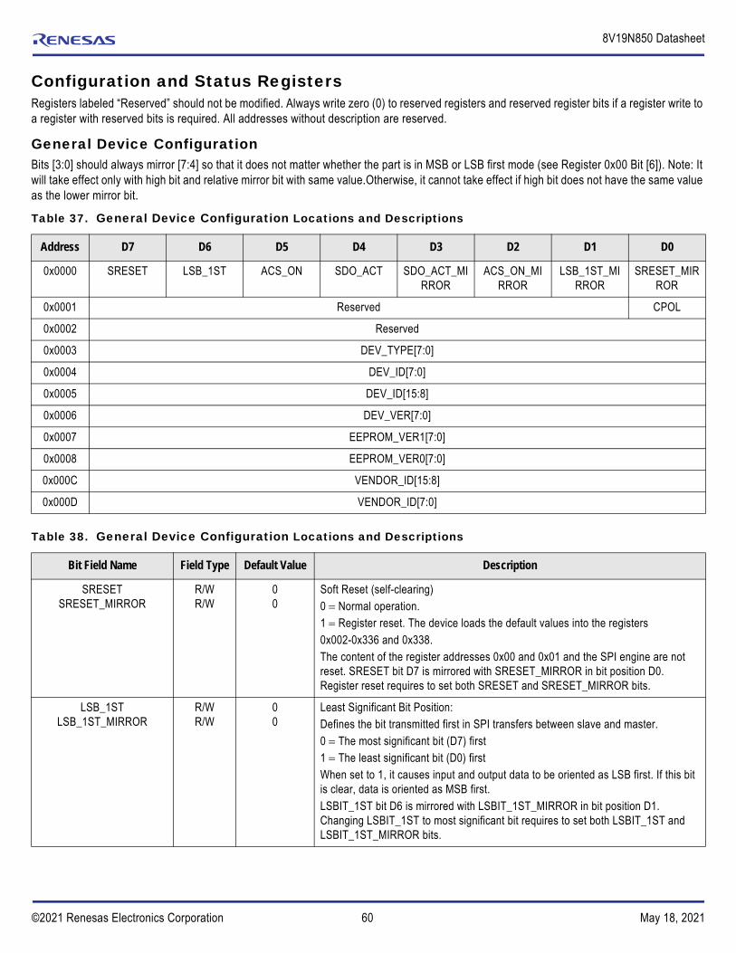
60©2021 Renesas Electronics Corporation May 18, 2021
8V19N850 Datasheet
Configuration and Status RegistersRegisters labeled “Reserved” should not be modified. Always write zero (0) to reserved registers and reserved register bits if a register write to a register with reserved bits is required. All addresses without description are reserved.
General Device ConfigurationBits [3:0] should always mirror [7:4] so that it does not matter whether the part is in MSB or LSB first mode (see Register 0x00 Bit [6]). Note: It will take effect only with high bit and relative mirror bit with same value.Otherwise, it cannot take effect if high bit does not have the same value as the lower mirror bit.
Table 37. General Device Configuration Locations and Descriptions
Address D7 D6 D5 D4 D3 D2 D1 D0
0x0000 SRESET LSB_1ST ACS_ON SDO_ACT SDO_ACT_MIRROR
ACS_ON_MIRROR
LSB_1ST_MIRROR
SRESET_MIRROR
0x0001 Reserved CPOL
0x0002 Reserved
0x0003 DEV_TYPE[7:0]
0x0004 DEV_ID[7:0]
0x0005 DEV_ID[15:8]
0x0006 DEV_VER[7:0]
0x0007 EEPROM_VER1[7:0]
0x0008 EEPROM_VER0[7:0]
0x000C VENDOR_ID[15:8]
0x000D VENDOR_ID[7:0]
Table 38. General Device Configuration Locations and Descriptions
Bit Field Name Field Type Default Value Description
SRESETSRESET_MIRROR
R/WR/W
00
Soft Reset (self-clearing)0 Normal operation.1 Register reset. The device loads the default values into the registers0x002-0x336 and 0x338. The content of the register addresses 0x00 and 0x01 and the SPI engine are not reset. SRESET bit D7 is mirrored with SRESET_MIRROR in bit position D0. Register reset requires to set both SRESET and SRESET_MIRROR bits.
LSB_1STLSB_1ST_MIRROR
R/WR/W
00
Least Significant Bit Position:Defines the bit transmitted first in SPI transfers between slave and master.0 The most significant bit (D7) first1 The least significant bit (D0) firstWhen set to 1, it causes input and output data to be oriented as LSB first. If this bit is clear, data is oriented as MSB first.LSBIT_1ST bit D6 is mirrored with LSBIT_1ST_MIRROR in bit position D1. Changing LSBIT_1ST to most significant bit requires to set both LSBIT_1ST and LSBIT_1ST_MIRROR bits.

61©2021 Renesas Electronics Corporation May 18, 2021
8V19N850 Datasheet
ACS_ONACS_ON_MIRROR
R/WR/W
00
Address Ascend on0 Address ascend is off (addresses auto-decrement)1 Address ascend is on (addresses auto-increment)The ASC_ON bit specifies whether addresses are incremented or decremented in streaming SPI transfers. ASC_ON bit D5 is mirrored with ASC_ON in bit position D2. Changing ASC_ON to “ON” requires to set both ASC_ON and ASC_ON_MIRROR bits.
SDO_ACTSDO_ACT_MIRROR
R/WR/W
11
SPI 3/4 Wire ModeSelects the unidirectional or bidirectional data transfer mode for the SDIO pin.0 = SPI 3-wire mode:
– SDIO is the SPI bidirectional data I/O pin– SDO pin is not used and is in high-impedance
1 = SPI 4-wire mode– SDIO is the SPI data input pin– SDO is the SPI data output pin
SDO_ACT bit D4 is mirrored with SDO_ACT_MIRROR in bit position D3. Changing SDO_ACT to SPI 4-wire mode requires to set both SDO_ACT and SDO_ACT_MIRROR bits.
CPOL R/W 0 Read Operation SCLK Polarity0 = Data bits on SDAT are output at the falling edge of SCLK edge
(SPI master will capture data on the rising edge of SCLK)1 = Data bits on SDAT are output at the rising edge of SCLK edge
(SPI master will capture data on the falling edge of SCLK)
Reserved R/W 0 Reserved. Do not modify this value.
DEV_TYPE[7:0] R/O 0110b Device type: set to 0x06: Device is a PLL
DEV_ID[15:0] R/O 0x0043 Device Identifier = 0x43
DEV_VER[7:0] R/O 3 Device Version = 0x03
EEPROM_VER1[7:0] R/W - These bytes are copied from an external EEPROM from the same offset address and can be used as EEPROM version information. Both EEPROM_VER0,1 registers should not be overwritten by a serial interface write access.Bytes are reserved if the device is not auto-configured from an EEPROM.
EEPROM_VER0[7:0] R/W -
VENDOR_ID[15:0] R/O 0x0426 Vendor Identifier:0x0426 (Renesas/IDT). Reads 0x0426 (Renesas/IDT) after power-up and reset.
Table 38. General Device Configuration Locations and Descriptions
Bit Field Name Field Type Default Value Description

62©2021 Renesas Electronics Corporation May 18, 2021
8V19N850 Datasheet
General Power Down RegistersTable 39. General Power Down Bit Field Locations and Descriptions
Address D7 D6 D5 D4 D3 D2 D1 D0
0x0011 Reserved SYSAPLL_PWN
SYSDPLL_PWN
DPLL1_PWN DPLL0_PWN DPLL_RST DPLL_UPDATE_RATE
Table 40. General Power Down Bit Field Locations
Bit Field Name Field Type Default Value Description
Reserved R/W 0 Reserved. Do not modify this value.
SYSDPLL_PWN R/W 0 System DPLL power down0 = SYS-DPLL is powered on1 = SYS-DPLL is powered down
DPLL1_PWN R/W 0 DPLL-1 power down0 = DPLL-1 is powered on1 = DPLL-1 is powered down
DPLL0_PWN R/W 0 DPLL-0 power down0 = DPLL-0 is powered on1 = DPLL-0 is powered down
DPLL_RST R/W 0 Reset the functional blocks REF_MON0, REF_MON1 (reference monitors for inputs CLK_0 and CLK_1), SYS-DPLL, DPLL-0, DPLL-1 including the DPLL-0/1 fractional feedback dividers.0 = Normal operation1 = Reset
DPLL_UPDATE_RATE R/W 0 Reserved
SYSAPLL_PWN R/W 0 System APLL power down0 = SYS-APLL is powered on1 = SYS-APLL is powered downSystem APLL can be powered down if the device does not use input clock signals at CLK_0 and CLK_1, and DPLL-0 and DPLL_1 are used as DCOs. When the SYS-APLL is powered down, the internal system clocks for the serial interfaces are automatically derived from VCO-0 or VCO-1.

63©2021 Renesas Electronics Corporation May 18, 2021
8V19N850 Datasheet
Read EEPROM Status
I/O Voltage Select Configuration
Table 41. Read EEPROM Status Bit Field Locations
Address D7 D6 D5 D4 D3 D2 D1 D0
0x0012 Reserved CHK_SUM_ERR_STS
RD_EEPROM_ABORT_ST
S
RD_EEPROM_ACTIVE_ST
S
DEVICE_RDY_STS
RD_EEPROM_RELOCK_INIT_DONE_ST
S
RD_EEPROM_DONE_STS
Table 42. Read EEPROM Status Bit Field Descriptions
Bit Field Name Field Type Default Value Description
CHK_SUM_ERR_STS R/O 0 Check sum error reading EEPROM0 = Check sum pass1 = Check sum fail
RD_EEPROM_ABORT_STS R/O 0 1 = Indicates EEPROM read aborted because I2C master lost bus access or EEPROM did not respond
RD_EEPROM_ACTIVE_STS
R/O 0 1 = Indicates reading from EEPROM is in progress
DEVICE_RDY_STS R/O 0 1 = Indicates device has finished initialization
RD_EEPROM_RELOCK_INIT_DONE_STS
R/O 0 1 = Indicates reading from EEPROM, relock, and asserting INIT_CLK_A/B/C/D is completed
RD_EEPROM_DONE_STS R/O 0 1 = Indicates reading from EEPROM is completed
Table 43. I/O Voltage Select Configuration Bit Field Locations
Address D7 D6 D5 D4 D3 D2 D1 D0
0x0013 Reserved SELSV2 SELSV1 SELSV0
Table 44. I/O Voltage Select Configuration Bit Field Descriptions
Bit Field Name Field Type Default Value Description
SELSV2 R/W 0 This bit configures GPIO I/O to be compatible with 1.8V or 3.3V0 = Compatible with 1.8V1 = Compatible with 3.3V
SELSV1 R/W 0 Reserved
SELSV0 R/W 0 This bit configures SDI (SPI data OUTPUT ONLY) and SDO_SDA (as SPI SDO output only) to be compatible with 1.8V or 3.3V. 0 = Compatible with 1.8V1 = Compatible with 3.3V

64©2021 Renesas Electronics Corporation May 18, 2021
8V19N850 Datasheet
System APLL (SYS-APLL) ConfigurationTable 45. SYS-APLL Configuration Bit Field Locations
Address D7 D6 D5 D4 D3 D2 D1 D0
0x0020 Reserved Reserved
0x0021 Reserved Reserved
0x0022 Reserved Reserved Reserved Reserved
0x0023 M_INT_SA[7:0]
0x0024 M_NUM_SA[7:0]
0x0025 M_NUM_SA[15:8]
0x0028 M_DEN_SA[7:0]
0x0029 M_DEN_SA[15:8]
0x002C Reserved Reserved Reserved Reserved Reserved
0x002D Reserved
0x002E Reserved
0x002F Reserved
Table 46. SYS-APLL Configuration Bit Field Descriptions
Bit Field Name Field Type Default Value Description
M_INT_SA[7:0] R/W 0x24 Integer portion of the SYS-APLL fractional feedback divider (binary coding)
M_NUM_SA[15:0] R/W 0 Numerator portion of the SYS-APLL fractional feedback divider (binary coding)
M_DEN_SA[15:0] R/W 0x8000 Denominator portion of the SYS-APLL fractional feedback divider (binary coding)

65©2021 Renesas Electronics Corporation May 18, 2021
8V19N850 Datasheet
System DPLL (SYS-DPLL) ConfigurationTable 47. SYS-DPLL State Bit Field Locations
Offset Address D7 D6 D5 D4 D3 D2 D1 D0
0x0044 SYSDPLL_TDC_FB[1:0] Reserved DPLL_STATE_SYSDPLL_CNFG[2:0]
0x0046 Reserved LOCK_STS_SYSDPLL
DPLL_STATE_STS_SYSDPLL[2:0]
0x0047 FILTER_STS_SYSDPLL[7:0]
0x0048 FILTER_STS_SYSDPLL[15:8]
0x0049 FILTER_STS_SYSDPLL[23:16]
0x004A FILTER_STS_SYSDPLL[31:24]
0x004B FILTER_STS_SYSDPLL[39:32]
0x004C FILTER_STS_SYSDPLL[47:40]
0x004D PHASE_STS_SYSDPLL[7:0]
0x004E PHASE_STS_SYSDPLL[15:8]
0x004F PHASE_STS_SYSDPLL[23:16]
0x0050 PHASE_STS_SYSDPLL[31:24]
0x0051 Reserved PHASE_STS_SYSDPLL[35:32]
Table 48. SYS-DPLL State Bit Field Descriptions
Bit Field Name Field Type Default Value Description
SYSDPLL_TDC_FB[1:0] R/W 00 SYSDPLL TDC feedback control00/11 = SYS-DPLL feedback01 = CLK_010 = CLK_1
DPLL_STATE_SYSDPLL_CNFG[2:0]
R/W 000 State of the SYS-DPLL 000 = Freerun001 = Lock acquisition010 = Normal lock011 = Holdover100 = Lock recovery 101 = Auto cnfg
LOCK_STS_SYSDPLL R/O 0 SYS-DPLL lock status0 = Unlocked1 = Locked
DPLL_STATE_STS_SYSDPLL[2:0]
R/O 000 SYS-DPLL states:000 = Freerun001 = Lock acquisition010 = Normal lock011 = Holdover100 = Lock recovery

66©2021 Renesas Electronics Corporation May 18, 2021
8V19N850 Datasheet
System DPLL (SYS-DPLL) Lock Threshold, Lock Timer, Bandwidth
FILTER_STS_SYSDPLL[47:0] R/O 0x0 SYS-DPLL Filter status48-bit 2's complementLSB = 2^-53 = 1.11e-7ppb
PHASE_STS_SYSDPLL[35:0] R/O 0x0 SYS-DPLL phase output of TDC phase status36-bit 2's complementLSB = TSYSAPLL_VCO / 62 (TDC step) phase data from decimator
Table 49. SYS-DPLL Lock Threshold, Lock Timer, Bandwidth Locations
Offset Address D7 D6 D5 D4 D3 D2 D1 D0
0x0052 LOCK_THRESHOLD_SYSDPLL[7:0]
0x0053 LOCK_THRESHOLD_SYSDPLL[15:8]
0x0054 LOCK_TIMER_SYSDPLL[7:0]
0x0055 AA_BW_SHIFT_SYSDPLL[4:0] AA_BW_MULT_SYSDPLL[2:0]
0x0056 NORMAL_BW_SHIFT_SYSDPLL[4:0] NORMAL_BW_MULT_SYSDPLL[2:0]
0x0057 Reserved NORMAL_DAMPING_SHIFT_SYSDPLL[2:0] NORMAL_DAMPING_MULT_SYSDPLL[2:0]
0x0058 ACQ_BW_SHIFT_SYSDPLL[4:0] ACQ_BW_MULT_SYSDPLL[2:0]
0x0059 Reserved ACQ_DAMPING_SHIFT_SYSDPLL[2:0] ACQ_DAMPING_MULT_SYSDPLL[2:0]
0x005A Reserved FILTER_STS_SELECT_SYSDPLL[1:0]
Table 50. SYS-DPLL Lock Threshold, Lock Timer, Bandwidth Descriptions
Bit Field Name Field Type Default Value Description
LOCK_THRESHOLD_SYSDPLL[15:0]
R/W 0x0115 SYS-DPLL Lock detector threshold.lock threshold 16-bit unsignedLSB = TSYSAPLL_VCO / 62 (TDC step)
LOCK_TIMER_SYSDPLL[7:0]
R/W 0x0A SYS-DPLL lock timer8-bit, unsignedLock timer = (LOCK_TIMER_SYSDPLL[7:0]2^8)/update_rateThe range is from 2ms to 512ms in step of 2ms assuming SYS_CLK is 108MHz.If phase error is within lock_threshold for the period that the timer is set, then the dpll is declared lock
Table 48. SYS-DPLL State Bit Field Descriptions
Bit Field Name Field Type Default Value Description
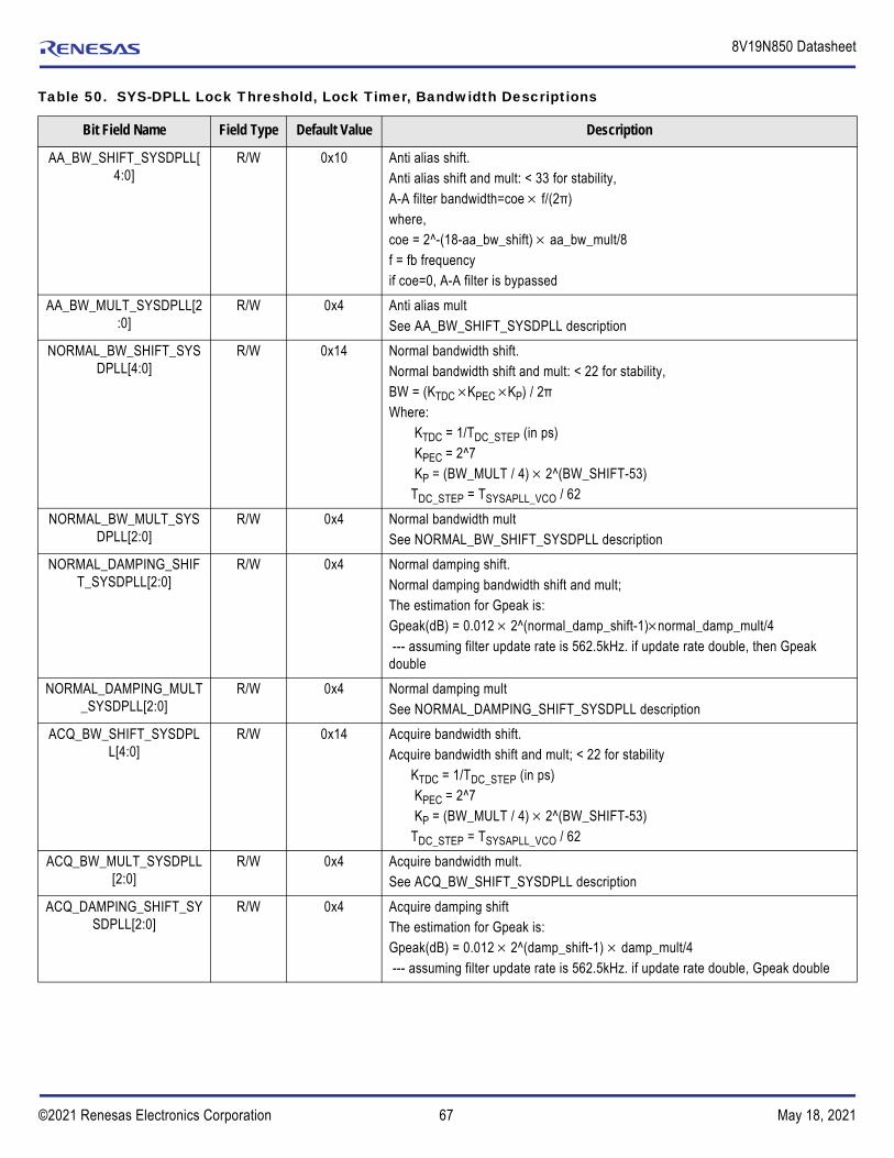
67©2021 Renesas Electronics Corporation May 18, 2021
8V19N850 Datasheet
AA_BW_SHIFT_SYSDPLL[4:0]
R/W 0x10 Anti alias shift.Anti alias shift and mult: < 33 for stability, A-A filter bandwidth=coe f/(2π)where,coe = 2^-(18-aa_bw_shift) aa_bw_mult/8f = fb frequencyif coe=0, A-A filter is bypassed
AA_BW_MULT_SYSDPLL[2:0]
R/W 0x4 Anti alias multSee AA_BW_SHIFT_SYSDPLL description
NORMAL_BW_SHIFT_SYSDPLL[4:0]
R/W 0x14 Normal bandwidth shift.Normal bandwidth shift and mult: < 22 for stability, BW = (KTDC KPEC KP) / 2πWhere:
KTDC = 1/TDC_STEP (in ps) KPEC = 2^7 KP = (BW_MULT / 4) 2^(BW_SHIFT-53)TDC_STEP = TSYSAPLL_VCO / 62
NORMAL_BW_MULT_SYSDPLL[2:0]
R/W 0x4 Normal bandwidth multSee NORMAL_BW_SHIFT_SYSDPLL description
NORMAL_DAMPING_SHIFT_SYSDPLL[2:0]
R/W 0x4 Normal damping shift.Normal damping bandwidth shift and mult; The estimation for Gpeak is:Gpeak(dB) = 0.012 2^(normal_damp_shift-1)normal_damp_mult/4 --- assuming filter update rate is 562.5kHz. if update rate double, then Gpeak double
NORMAL_DAMPING_MULT_SYSDPLL[2:0]
R/W 0x4 Normal damping multSee NORMAL_DAMPING_SHIFT_SYSDPLL description
ACQ_BW_SHIFT_SYSDPLL[4:0]
R/W 0x14 Acquire bandwidth shift.Acquire bandwidth shift and mult; < 22 for stability
KTDC = 1/TDC_STEP (in ps) KPEC = 2^7 KP = (BW_MULT / 4) 2^(BW_SHIFT-53)TDC_STEP = TSYSAPLL_VCO / 62
ACQ_BW_MULT_SYSDPLL[2:0]
R/W 0x4 Acquire bandwidth mult.See ACQ_BW_SHIFT_SYSDPLL description
ACQ_DAMPING_SHIFT_SYSDPLL[2:0]
R/W 0x4 Acquire damping shiftThe estimation for Gpeak is:Gpeak(dB) = 0.012 2^(damp_shift-1)damp_mult/4 --- assuming filter update rate is 562.5kHz. if update rate double, Gpeak double
Table 50. SYS-DPLL Lock Threshold, Lock Timer, Bandwidth Descriptions
Bit Field Name Field Type Default Value Description

68©2021 Renesas Electronics Corporation May 18, 2021
8V19N850 Datasheet
System DPLL (SYS-DPLL) Phase Error Compensation (PEC) and Frequency Divider
ACQ_DAMPING_MULT_SYSDPLL[2:0]
R/W 0x4 Acquire damping mult.See ACQ_DAMPING_SHIFT_SYSDPLL description
FILTER_STS_SELECT_SYSDPLL[1:0]
R/W 0 Selects source of the filter status register; 0 = Integrator1 = Proportional + integrator2 = Holdover value3 = fcw
Table 51. SYS-DPLL Phase Error Compensation and Frequency Divider Bit Field Locations
Offset Address D7 D6 D5 D4 D3 D2 D1 D0
0x005B PEC_CORR_SYSDPLL[7:0]
0x005C PEC_DELAY_SYSDPLL[1:0] PEC_CORR_SYSDPLL[13:8]
0x005E M_INT_SD[7:0]
0x005F Reserved M_INT_SD[9:8]
0x0060 M_NUM_SD[7:0]
0x0061 M_NUM_SD[15:8]
0x0062 M_DEN_SD[7:0]
0x0063 M_DEN_SD[15:8]
Table 52. SYS-DPLL Phase Error Compensation and Frequency Divider Bit Field Descriptions
Bit Field Name Field Type Default Value Description
PEC_CORR_SYSDPLL[13:0]
R/W 0 Phase error cancellation (PEC) to compensate the phase error from the 1st-order modulated fractional feedback divider. The residual part of the fractional feedback is scaled to TDC resolution and is compensated to the TDC phase error.PEC scale factor for using CLK_0 as input:PEC_CORR = (TVCO ÷ TDC_STEP) × 2DEN_BITS/DEN
where:TVCO: period of the feedback divider input clock TDC_STEP: TDC step sizeDEN_BITS: total number of bits of denominator bits (16 bits for the SYS-DPLL)DEN: denominator (M_DEN_SD[15:0])
M_INT_SD[9:0] R/W 0x56 Integer portion of the SYS-DPLL fractional feedback divider (binary coding)
M_NUM_SD[15:0] R/W 0x2000 Numerator portion of the SYS-DPLL fractional feedback divider (binary coding)
M_DEN_SD[15:0] R/W 0x5000 Denominator portion of the SYS-DPLL fractional feedback divider (binary coding)
Table 50. SYS-DPLL Lock Threshold, Lock Timer, Bandwidth Descriptions
Bit Field Name Field Type Default Value Description

69©2021 Renesas Electronics Corporation May 18, 2021
8V19N850 Datasheet
Reference Monitor for Input CLK_0Table 53. Reference Monitor CLK_0 Field Descriptions
Offset Address D7 D6 D5 D4 D3 D2 D1 D0
0x0080 Reserved DIV_RATIO_ST_REF_MON0[5:0]
0x0081 NOMINAL_NUM_ST_REF_MON0[7:0]
0x0082 ACCEPT_NUM_ST_REF_MON0[3:0] REJECT_NUM_ST_REF_MON0[3:0]
0x0083 GOOD_TIMES_ST_REF_MON0[3:0] FAIL_NUM_ST_REF_MON0[3:0]
0x0084 DIV_RATIO_MT_REF_MON0[7:0]
0x0085 DIV_RATIO_MT_REF_MON0[15:8]
0x0086 NOMINAL_NUM_MT_REF_MON0[7:0]
0x0087 NOMINAL_NUM_MT_REF_MON0[15:8]
0x0088 Reserved NOMINAL_NUM_MT_REF_MON0[17:16]
0x0089 ACCEPT_NUM_MT_REF_MON0[7:0]
0x008A ACCEPT_NUM_MT_REF_MON0[15:8]
0x008B REJECT_NUM_MT_REF_MON0[7:0]
0x008C REJECT_NUM_MT_REF_MON0[15:8]
0x008D GOOD_TIMES_MT_REF_MON0[3:0] FAIL_NUM_MT_REF_MON0[3:0]
0x008E DIV_RATIO_LT_REF_MON0[7:0]
0x008F DIV_RATIO_LT_REF_MON0[15:8]
0x0090 DIV_RATIO_LT_REF_MON0[23:16]
0x0091 Reserved DIV_RATIO_LT_REF_MON0[28:24]
0x0092 NOMINAL_NUM_LT_REF_MON0[7:0]
0x0093 NOMINAL_NUM_LT_REF_MON0[15:8]
0x0094 NOMINAL_NUM_LT_REF_MON0[23:16]
0x0095 NOMINAL_NUM_LT_REF_MON0[31:24]
0x0096 ACCEPT_NUM_LT_REF_MON0[7:0]
0x0097 ACCEPT_NUM_LT_REF_MON0[15:8]
0x0098 Reserved ACCEPT_NUM_LT_REF_MON0[21:16]
0x0099 REJECT_NUM_LT_REF_MON0[7:0]
0x009A REJECT_NUM_LT_REF_MON0[15:8]
0x009B Reserved REJECT_NUM_LT_REF_MON0[21:16]
0x009C GOOD_TIMES_LT_REF_MON[3:0] FAIL_NUM_LT_REF_MON0[3:0]
0x009D PD_CLK0 DIS_CLK0 DIS_CLK0_BY_PIN
Reserved R0[2:0]

70©2021 Renesas Electronics Corporation May 18, 2021
8V19N850 Datasheet
0x009E Reserved SRC_SEL_LT_REF_MON0[1:0]
0x009F FREQ_NUMBER_STS_REF_MON0[7:0]
0x00A0 FREQ_NUMBER_STS_REF_MON0[15:8]
0x00A1 FREQ_NUMBER_STS_REF_MON0[23:16]
Table 54. Reference Monitor CLK_0 Field Descriptions
Bit Field Name Field Type Default Value Description
DIV_RATIO_ST_REF_MON0[5:0]
R/W 1 Short-term monitor divider ratio is used for monitoring the activity of input reference clock for frequencies higher than 1MHz.If DIV_RATIO_ST_REF_MON0 is set to 0 or 1, the actual short-term monitor divider ratio is 1. Otherwise short-term monitor divider ratio = DIV_RATIO_ST_REF_MON0 +2
NOMINAL_NUM_ST_REF_MON0[7:0]
R/W 0x6E Nominal number of SYS_CLK cycles within the counter window, which is:fSYS_CLK/(fREF/div_ratio).
ACCEPT_NUM_ST_REF_MON0[3:0]
R/W 0xB Accept number, if counter value is within nominal_num ± accept_num, then the good counter increases by 1, and the fail counter is cleared.
REJECT_NUM_ST_REF_MON0[3:0]
R/W 0xF Reject number, if counter value outside nominal_num ± reject_num, then fail counter increases by 1, and the good timer is cleared.
GOOD_TIMES_ST_REF_MON0[3:0]
R/W 0x4 Number of times cycle is within window before it is reported as good. If good counter reaches the number programmed in these bits, then the reference is declared good.To declare a reference to be qualified, it must be detected good continuously for the number of good times
FAIL_NUM_ST_REF_MON0[3:0]
R/W 0x1 If failure time reaches the number programmed in these bits, then the reference is declared fail, set alarm and interrupt.
DIV_RATIO_MT_REF_MON0[15:0]
R/W 0x4B00 Medium-term monitor divider ratio is used for medium-term monitoringIf DIV_RATIO_NT_REF_MON0 is set to 0 or 1, the actual medium-term monitor divider ratio is 1. Otherwise medium-term monitor divider ratio = DIV_RATIO_MT_REF_MON0 +2
NOMINAL_NUM_MT_REF_MON0[17:0]
R/W 0x20F58 Nominal number of SYS_CLK cycles within the counter window, which is:fSYS_CLK/(fREF/div_ratio)
ACCEPT_NUM_MT_REF_MON0[15:0]
R/W 0x83D6 Accept number, if counter value is within norminal_num ± accept_num, then the good counter increases by 1, and the fail counter is cleared
REJECT_NUM_MT_REF_MON0[15:0]
R/W 0xB892 Reject number, if counter value outside norminal_num ± reject_num, then the fail counter increases by 1, and the good timer is cleared.
GOOD_TIMES_MT_REF_MON0[3:0]
R/W 0100 Number of times cycle is within window before it is reported as good. If good counter reaches the number programmed in these bits, then the reference is declared good.To declare a reference to be qualified, it must be detected good continuously for the number of good times.
FAIL_NUM_MT_REF_MON0[3:0]
R/W 0001 If medium-term monitor failure time reaches the number programmed in these bits, then the reference is declared fail, set alarm and interrupt.
Table 53. Reference Monitor CLK_0 Field Descriptions (Cont.)
Offset Address D7 D6 D5 D4 D3 D2 D1 D0

71©2021 Renesas Electronics Corporation May 18, 2021
8V19N850 Datasheet
DIV_RATIO_LT_REF_MON0[28:0]
R/W 0x0927C000 Long-term monitor divider ratio is used for long-term monitoringIf DIV_RATIO_LT_REF_MON0 is set to 0 or 1, the actual long-term monitor divider ratio is 1. Otherwise long-term monitor divider ratio = DIV_RATIO_MT_REF_MON0 +2
NOMINAL_NUM_LT_REF_MON0[31:0]
R/W 0x405F7E00 Nominal number of SYS_CLK cycles within the counter window, which is:fSYS_CLK/(fREF/div_ratio)
ACCEPT_NUM_LT_REF_MON0[21:0]
R/W 0x0032A0 Accept number, if counter value is within norminal_num ± accept_num, then the good counter increases by 1, and the fail counter is cleared.
REJECT_NUM_LT_REF_MON0[21:0]
R/W 0x003B10 Reject number, if counter value is outside norminal_num ± reject_num, fail = 1, then the fail counter increases by 1, and the good timer is cleared.
GOOD_TIMES_LT_REF_MON0[3:0]
R/W 0100 Number of times cycle is within window before it is reported as good. If good counter reaches the number programmed in these bits, then the reference is declared good.To declare a reference to be qualified, it must be detected good continuously for the number of good times.
FAIL_NUM_LT_REF_MON0[3:0]
R/W 0001 If long-term monitor failure time reaches the number programmed in these bits, then the reference is declared fail, set alarm and interrupt.
PD_CLK0 R/W 1 Power down ref clock path.0 = CLK_0 path is powered on1 = CLK_0 path is powered off
DIS_CLK0 R/W 0 This bit disables input CLK_0 reference from being selected for DPLL-0 and DPLL-1 to lock to it.0 = CLK_0 reference can be selected1 = CLK_0 reference can not be selected
DIS_CLK0_BY_PIN R/W 0 If this bit is set, then GPIO can be used to enable or disable input CLK_0 reference to be selected for DPLL-0 and DPLL-1 to lock to it.0 = CLK_0 reference can be disabled by bit DIS_CLK01 = CLK_0 reference can be disabled by GPIO
R0[2:0] R/W 000 Input CLK_0 reference clock high frequency pre-divider. The reference frequency must be divided down to a maximum of SYS_CLK ÷ 3 (< 36MHz) by the high frequency pre-divider.000 = ÷1001 = ÷2010 = ÷4011 = ÷8100 = ÷16101 = ÷32
Table 54. Reference Monitor CLK_0 Field Descriptions (Cont.)
Bit Field Name Field Type Default Value Description

72©2021 Renesas Electronics Corporation May 18, 2021
8V19N850 Datasheet
SRC_SEL_LT_REF_MON0[1:0]
R/W 00 Long term reference monitor clock source selection for CLK_000 = SYS_CLK01 = OSCI/OSCO (crystal oscillator)1x = XO_DPLL
FREQ_NUMBER_STS_REF_MON0[23:0]
R/O 0 Status of the frequency monitor counter (2's complement)This register is 24-bit signed, it represents the reference clock fractional frequency offset with respect to the SYS_CLK or optionally OSCI/OSCO/XO_DPLL. The frequency offset in ppm is:1062-32 FREQ_NUMBER_STS_REF_MON0[23:0] The LSB is 2-32106 ppm.
Table 54. Reference Monitor CLK_0 Field Descriptions (Cont.)
Bit Field Name Field Type Default Value Description

73©2021 Renesas Electronics Corporation May 18, 2021
8V19N850 Datasheet
Reference Monitor for Input CLK_1Table 55. Reference Monitor CLK_1 Field Locations
Offset Address D7 D6 D5 D4 D3 D2 D1 D0
0x00B0 Reserved DIV_RATIO_ST_REF_MON1[5:0]
0x00B1 NOMINAL_NUM_ST_REF_MON1[7:0]
0x00B2 ACCEPT_NUM_ST_REF_MON1[3:0] REJECT_NUM_ST_REF_MON1[3:0]
0x00B3 GOOD_TIMES_ST_REF_MON1[3:0] FAIL_NUM_ST_REF_MON1[3:0]
0x00B4 DIV_RATIO_MT_REF_MON1[7:0]
0x00B5 DIV_RATIO_MT_REF_MON1[15:8]
0x00B6 NOMINAL_NUM_MT_REF_MON1[7:0]
0x00B7 NOMINAL_NUM_MT_REF_MON1[15:8]
0x00B8 Reserved NOMINAL_NUM_MT_REF_MON1[17:16]
0x00B9 ACCEPT_NUM_MT_REF_MON1[7:0]
0x00BA ACCEPT_NUM_MT_REF_MON1[15:8]
0x00BB REJECT_NUM_MT_REF_MON1[7:0]
0x00BC REJECT_NUM_MT_REF_MON1[15:8]
0x00BD GOOD_TIMES_MT_REF_MON1[3:0] FAIL_NUM_MT_REF_MON1[3:0]
0x00BE DIV_RATIO_LT_REF_MON1[7:0]
0x00BF DIV_RATIO_LT_REF_MON1[15:8]
0x00C0 DIV_RATIO_LT_REF_MON1[23:16]
0x00C1 Reserved DIV_RATIO_LT_REF_MON1[28:24]
0x00C2 NOMINAL_NUM_LT_REF_MON1[7:0]
0x00C3 NOMINAL_NUM_LT_REF_MON1[15:8]
0x00C4 NOMINAL_NUM_LT_REF_MON1[23:16]
0x00C5 NOMINAL_NUM_LT_REF_MON1[31:24]
0x00C6 ACCEPT_NUM_LT_REF_MON1[7:0]
0x00C7 ACCEPT_NUM_LT_REF_MON1[15:8]
0x00C8 Reserved ACCEPT_NUM_LT_REF_MON1[21:16]
0x00C9 REJECT_NUM_LT_REF_MON1[7:0]
0x00CA REJECT_NUM_LT_REF_MON1[15:8]
0x00CB Reserved REJECT_NUM_LT_REF_MON1[21:16]
0x00CC GOOD_TIMES_LT_REF_MON1[3:0] FAIL_NUM_LT_REF_MON1[3:0]
0x00CD PD_CLK1 DIS_CLK1 DIS_CLK1_BY_PIN
Reserved R1[2:0]

74©2021 Renesas Electronics Corporation May 18, 2021
8V19N850 Datasheet
0x00CE Reserved SRC_SEL_LT_REF_MON1[1:0]
0x00CF FREQ_NUMBER_STS_REF_MON1[7:0]
0x00D0 FREQ_NUMBER_STS_REF_MON1[15:8]
0x00D1 FREQ_NUMBER_STS_REF_MON1[23:16]
Table 56. Reference Monitor CLK_1 Field Descriptions
Bit Field Name Field Type Default Value Description
DIV_RATIO_ST_REF_MON1[5:0]
R/W 6 Short-term monitor divider ratio is used for monitoring the activity of input reference clock for frequencies higher than 1MHz.If DIV_RATIO_ST_REF_MON1 is set to 0 or 1, the actual short-term monitor divider ratio is 1. Otherwise short-term monitor divider ratio = DIV_RATIO_ST_REF_MON1 +2
NOMINAL_NUM_ST_REF_MON1[7:0]
R/W 0x2E Nominal number of SYS_CLK cycles within the counter window, which is:fSYS_CLK/(fREF/div_ratio)
ACCEPT_NUM_ST_REF_MON1[3:0]
R/W 1000 Accept number, if counter value is within nominal_num ± accept_num, then the good counter increases by 1, and the fail counter is cleared.
REJECT_NUM_ST_REF_MON1[3:0]
R/W 1111 Reject number, if counter value outside nominal_num ± reject_num, then fail counter increases by 1, and the good timer is cleared.
GOOD_TIMES_ST_REF_MON1[3:0]
R/W 0100 Number of times cycle is within window before it is reported as good. If good counter reaches the number programmed in these bits, then the reference is declared good.To declare a reference to be qualified, it must be detected good continuously for the number of good times.
FAIL_NUM_ST_REF_MON1[3:0]
R/W 0001 If failure time reaches the number programmed in these bits, then the reference is declared fail, set alarm and interrupt.
DIV_RATIO_MT_REF_MON1[15:0]
R/W 0x4B00 Medium-term monitor divider ratio is used for medium-term monitoringIf DIV_RATIO_NT_REF_MON1 is set to 0 or 1, the actual medium-term monitor divider ratio is 1. Otherwise medium-term monitor divider ratio = DIV_RATIO_MT_REF_MON1 +2
NOMINAL_NUM_MT_REF_MON1[17:0]
R/W 0x20F58 Nominal number of SYS_CLK cycles within the counter window, which is:fSYS_CLK/(fREF/div_ratio).
ACCEPT_NUM_MT_REF_MON1[15:0]
R/W 0x83D6 Accept number, if counter value is within norminal_num ± accept_num, then the good counter increases by 1, and the fail counter is cleared.
REJECT_NUM_MT_REF_MON1[15:0]
R/W 0xB892 Reject number, if counter value outside norminal_num ± reject_num, then the fail counter increases by 1, and the good timer is cleared.
GOOD_TIMES_MT_REF_MON1[3:0]
R/W 0100 Number of times cycle is within window before it is reported as good. If good counter reaches the number programmed in these bits, then the reference is declared good.To declare a reference to be qualified, it must be detected good continuously for the number of good times.
FAIL_NUM_MT_REF_MON1[3:0]
R/W 0001 If medium-term monitor failure time reaches the number programmed in these bits, then the reference is declared fail, set alarm and interrupt.
Table 55. Reference Monitor CLK_1 Field Locations (Cont.)
Offset Address D7 D6 D5 D4 D3 D2 D1 D0

75©2021 Renesas Electronics Corporation May 18, 2021
8V19N850 Datasheet
DIV_RATIO_LT_REF_MON1[28:0]
R/W 0x0927C000 Long-term monitor divider ratio is used for long-term monitoringIf DIV_RATIO_LT_REF_MON1 is set to 0 or 1, the actual long-term monitor divider ratio is 1. Otherwise long-term monitor divider ratio = DIV_RATIO_MT_REF_MON1 +2
NOMINAL_NUM_LT_REF_MON1[31:0]
R/W 405F7E00h Nominal number of SYS_CLK cycles within the counter window, which is:fSYS_CLK/(fREF/div_ratio).
ACCEPT_NUM_LT_REF_MON1[21:0]
R/W 0x0032A0 Accept number, if counter value is within norminal_num ± accept_num, then the good counter increases by 1, and the fail counter is cleared.
REJECT_NUM_LT_REF_MON1[21:0]
R/W 0x003B10 Reject number, if counter value is outside norminal_num ± reject_num, fail = 1, then the fail counter increases by 1, and the good timer is cleared.
GOOD_TIMES_LT_REF_MON1[3:0]
R/W 0100 Number of times cycle is within window before it is reported as good. If good counter reaches the number programmed in these bits, then the reference is declared good.To declare a reference to be qualified, it must be detected good continuously for the number of good times.
FAIL_NUM_LT_REF_MON1[3:0]
R/W 0001 If long-term monitor failure time reaches the number programmed in these bits, then the reference is declared fail, set alarm and interrupt.
PD_CLK1 R/W 1 Power down ref clock path.0 = CLK_1 path is powered on1 = CLK_1 path is powered off
DIS_CLK1 R/W 0 This bit disables input CLK_1 reference from being selected for DPLL-0 and DPLL-1 to lock to it.0 = CLK_1 reference can be selected1 = CLK_1 reference can not be selected
DIS_CLK1_BY_PIN R/W 0 If this bit is set, then GPIO can be used to enable or disable input CLK_1 reference to be selected for DPLL-0 and DPLL-1 to lock to it.0 = CLK_1 reference can be disabled by bit DIS_CLK11 = CLK_1 reference can be disabled by GPIO
R1[2:0] R/W 000 Input CLK_1 reference clock high frequency pre-divider. The reference frequency must be divided down to a maximum of SYS_CLK ÷ 3 (< 36MHz) by the high frequency pre-divider.000 = ÷1001 = ÷2010 = ÷4011 = ÷8100 = ÷16101 = ÷32
Table 56. Reference Monitor CLK_1 Field Descriptions (Cont.)
Bit Field Name Field Type Default Value Description
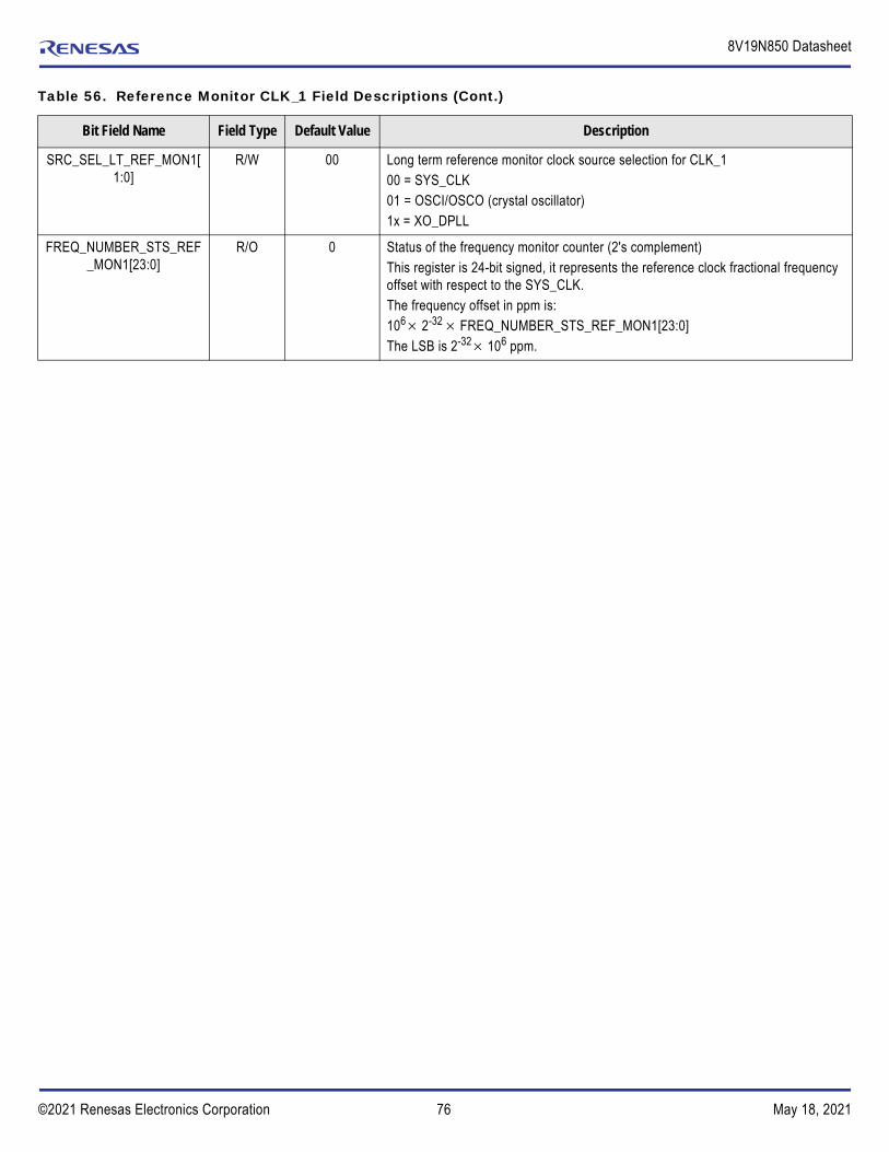
76©2021 Renesas Electronics Corporation May 18, 2021
8V19N850 Datasheet
SRC_SEL_LT_REF_MON1[1:0]
R/W 00 Long term reference monitor clock source selection for CLK_100 = SYS_CLK01 = OSCI/OSCO (crystal oscillator)1x = XO_DPLL
FREQ_NUMBER_STS_REF_MON1[23:0]
R/O 0 Status of the frequency monitor counter (2's complement)This register is 24-bit signed, it represents the reference clock fractional frequency offset with respect to the SYS_CLK. The frequency offset in ppm is:106 2-32FREQ_NUMBER_STS_REF_MON1[23:0] The LSB is 2-32 106 ppm.
Table 56. Reference Monitor CLK_1 Field Descriptions (Cont.)
Bit Field Name Field Type Default Value Description

77©2021 Renesas Electronics Corporation May 18, 2021
8V19N850 Datasheet
Global StatusTable 57. Globals Status Bit Field Locations
Offset Address D7 D6 D5 D4 D3 D2 D1 D0
0x00E0 Reserved CLK1_FAIL_ST_DISQUAL
_MASK
CLK1_FAIL_MT_DISQUAL
_MASK
CLK1_FAIL_LT_DISQUAL_
MASK
Reserved CLK0_FAIL_ST_DISQUAL_
MASK
CLK0_FAIL_MT_DISQUAL
_MASK
CLK0_FAIL_LT_DISQUAL_
MASK
0x00E1 CLK1_INVALID
CLK1_FAIL_ST
CLK1_FAIL_MT
CLK1_FAIL_LT
CLK0_INVALID
CLK0_FAIL_ST
CLK0_FAIL_MT
CLK0_FAIL_LT
0x00E2 Reserved CLK1_FAIL_ST_INT
CLK1_FAIL_MT_INT
CLK1_FAIL_LT_INT
Reserved CLK0_FAIL_ST_INT
CLK0_FAIL_MT_INT
CLK0_FAIL_LT_INT
0x00E3 Reserved DPLL1_STATE_CHANGE_I
NT
DPLL1_HOLDOVER_INT
DPLL1_LOSS_OF_LOCK_I
NT
Reserved DPLL0_STATE_CHANGE_I
NT
DPLL0_HOLDOVER_INT
DPLL0_LOSS_OF_LOCK_I
NT
0x00E4 Reserved SYSDPLL_STATE_CHANG
E_INT
SYSDPLL_HOLDOVER_I
NT
SYSDPLL_LOSS_OF_LOC
K_INT
RFPLL_LOSS_OF_LOCK_I
NT
APLL2_LOSS_OF_LOCK_I
NT
APLL1_LOSS_OF_LOCK_I
NT
APLL0_LOSS_OF_LOCK_I
NT
0x00E5 Reserved CLK1_FAIL_ST_MASK
CLK1_FAIL_MT_MASK
CLK1_FAIL_LT_MASK
Reserved CLK0_FAIL_ST_MASK
CLK0_FAIL_MT_MASK
CLK0_FAIL_LT_MASK
0x00E6 Reserved DPLL1_STATE_CHANGE_
MASK
DPLL1_HOLDOVER_MASK
DPLL1_LOSS_OF_LOCK_
MASK
Reserved DPLL0_STATE_CHANGE_
MASK
DPLL0_HOLDOVER_MASK
DPLL0_LOSS_OF_LOCK_
MASK
0x00E7 Reserved SYSDPLL_STATE_CHANG
E_MASK
SYSDPLL_HOLDOVER_M
ASK
SYSDPLL_LOSS_OF_LOC
K_MASK
RFPLL_LOSS_OF_LOCK_
MASK
APLL2_LOSS_OF_LOCK_
MASK
APLL1_LOSS_OF_LOCK_
MASK
APLL0_LOSS_OF_LOCK_
MASK
Table 58. Globals Status Bit Field Descriptions
Bit Field Name Field Type Default Value Description
CLK1_FAIL_ST_DISQUAL_MASK
R/W 0 If this bit is asserted, then short-term monitor failure does not disqualify CLK_10 = Not masked1 = Masked
CLK1_FAIL_MT_DISQUAL_MASK
R/W 0 If this bit is asserted, then medium-term monitor failure does not disqualify CLK_10 = Not masked1 = Masked
CLK1_FAIL_LT_DISQUAL_MASK
R/W 0 If this bit is asserted, then long-term monitor failure does not disqualify CLK_10 = Not masked1 = Masked
CLK0_FAIL_ST_DISQUAL_MASK
R/W 0 If this bit is asserted, then short-term monitor failure does not disqualify CLK_00 = Not masked1 = Masked
CLK0_FAIL_MT_DISQUAL_MASK
R/W 0 If this bit is asserted, then medium-term monitor failure does not disqualify CLK_00 = Not masked1 = Masked
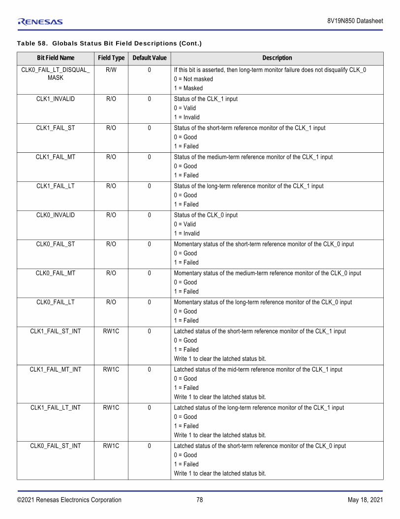
78©2021 Renesas Electronics Corporation May 18, 2021
8V19N850 Datasheet
CLK0_FAIL_LT_DISQUAL_MASK
R/W 0 If this bit is asserted, then long-term monitor failure does not disqualify CLK_00 = Not masked1 = Masked
CLK1_INVALID R/O 0 Status of the CLK_1 input0 = Valid1 = Invalid
CLK1_FAIL_ST R/O 0 Status of the short-term reference monitor of the CLK_1 input0 = Good1 = Failed
CLK1_FAIL_MT R/O 0 Status of the medium-term reference monitor of the CLK_1 input0 = Good1 = Failed
CLK1_FAIL_LT R/O 0 Status of the long-term reference monitor of the CLK_1 input0 = Good1 = Failed
CLK0_INVALID R/O 0 Status of the CLK_0 input0 = Valid1 = Invalid
CLK0_FAIL_ST R/O 0 Momentary status of the short-term reference monitor of the CLK_0 input0 = Good1 = Failed
CLK0_FAIL_MT R/O 0 Momentary status of the medium-term reference monitor of the CLK_0 input0 = Good1 = Failed
CLK0_FAIL_LT R/O 0 Momentary status of the long-term reference monitor of the CLK_0 input0 = Good1 = Failed
CLK1_FAIL_ST_INT RW1C 0 Latched status of the short-term reference monitor of the CLK_1 input0 = Good1 = FailedWrite 1 to clear the latched status bit.
CLK1_FAIL_MT_INT RW1C 0 Latched status of the mid-term reference monitor of the CLK_1 input0 = Good1 = FailedWrite 1 to clear the latched status bit.
CLK1_FAIL_LT_INT RW1C 0 Latched status of the long-term reference monitor of the CLK_1 input0 = Good1 = FailedWrite 1 to clear the latched status bit.
CLK0_FAIL_ST_INT RW1C 0 Latched status of the short-term reference monitor of the CLK_0 input0 = Good1 = FailedWrite 1 to clear the latched status bit.
Table 58. Globals Status Bit Field Descriptions (Cont.)
Bit Field Name Field Type Default Value Description

79©2021 Renesas Electronics Corporation May 18, 2021
8V19N850 Datasheet
CLK0_FAIL_MT_INT RW1C 0 Latched status of the mid-term reference monitor of the CLK_0 input0 = Good1 = FailedWrite 1 to clear the latched status bit.
CLK0_FAIL_LT_INT RW1C 0 Latched status of the long-term reference monitor of the CLK_0 input0 = Good1 = FailedWrite 1 to clear the latched status bit.
DPLL1_STATE_CHANGE_INT
RW1C 0 DPLL-1 state changed latched interrupt, indicates DPLL state changed
DPLL1_HOLDOVER_INT RW1C 0 DPLL-1 holdover latched interrupt, indicates holdover state changed, i.e. enter or exit holdover
DPLL1_LOSS_OF_LOCK_INT
RW1C 0 DPLL-1 loss of lock latched interrupt, indicates loss of lock detected.
Reserved RW1C 0 Reserved. Do not modify this value.
DPLL0_STATE_CHANGE_INT
RW1C 0 DPLL-0 state changed latched interrupt, indicates DPLL-0 state changed.
DPLL0_HOLDOVER_INT RW1C 0 DPLL-0 holdover latched interrupt, indicates holdover state changed, i.e. enter or exit holdover.
DPLL0_LOSS_OF_LOCK_INT
RW1C 0 DPLL-0 loss of lock latched interrupt, indicates loss of lock detected.
SYSDPLL_STATE_CHANGE_INT
RW1C 0 SYS-DPLL state changed latched interrupt, indicates SYS-DPLL state changed
SYSDPLL_HOLDOVER_INT
RW1C 0 SYS-DPLL holdover latched interrupt, indicates holdover state changed, i.e. enter or exit holdover.
SYSDPLL_LOSS_OF_LOCK_INT
RW1C 0 SYS-DPLL loss of lock latched interrupt, indicates loss of lock detected.
RFPLL_LOSS_OF_LOCK_INT
RW1C 0 RF-PLL loss of lock latched interrupt, indicates loss of lock detected.
APLL2_LOSS_OF_LOCK_INT
RW1C 0 APLL-2 loss of lock latched interrupt, indicates loss of lock detected.
APLL1_LOSS_OF_LOCK_INT
RW1C 0 APLL-1 loss of lock latched interrupt, indicates loss of lock detected.
APLL0_LOSS_OF_LOCK_INT
RW1C 0 APLL-0 loss of lock latched interrupt, indicates loss of lock detected.
CLK1_FAIL_ST_MASK R/W 0 Interrupt mask for the CLK_1 input short-term monitorIf this bit is asserted, a failure of the CLK_1 input short-term monitor does not generate an interrupt, and the short-term failure does not disqualify the CLK_1 reference. 0 = Short-term monitor interrupt is not masked1 = Short-term monitor interrupt is masked (no interrupt generated)
Table 58. Globals Status Bit Field Descriptions (Cont.)
Bit Field Name Field Type Default Value Description

80©2021 Renesas Electronics Corporation May 18, 2021
8V19N850 Datasheet
CLK1_FAIL_MT_MASK R/W 0 Interrupt mask for the CLK_1 input medium-term monitorIf this bit is asserted, a failure of the CLK_1 input medium-term monitor does not generate an interrupt, and the medium-term failure does not disqualify the CLK_1 reference. 0 = Medium-term monitor interrupt is not masked1 = Medium-term monitor interrupt is masked (no interrupt generated)
CLK1_FAIL_LT_MASK R/W 0 Interrupt mask for the CLK_1 input long-term monitorIf this bit is asserted, a failure of the CLK_1 input long-term monitor does not generate an interrupt, and the long-term failure does not disqualify the CLK_1 reference. 0 = Long-term monitor interrupt is not masked1 = Long-term monitor interrupt is masked (no interrupt generated)
CLK0_FAIL_ST_MASK R/W 0 Interrupt mask for the CLK_0 input short-term monitorIf this bit is asserted, a failure of the CLK_0 input short-term monitor does not generate an interrupt, and the short-term failure does not disqualify the CLK_0 reference. 0 = Short-term monitor interrupt is not masked1 = Short-term monitor interrupt is masked (no interrupt generated)
CLK0_FAIL_MT_MASK R/W 0 Interrupt mask for the CLK_0 input medium-term monitorIf this bit is asserted, a failure of the CLK_0 input medium-term monitor does not generate an interrupt, and the medium-term failure does not disqualify the CLK_0 reference. 0 = Medium-term monitor interrupt is not masked1 = Medium-term monitor interrupt is masked (no interrupt generated)
CLK0_FAIL_LT_MASK R/W 0 Interrupt mask for the CLK_0 input long-term monitorIf this bit is asserted, a failure of the CLK_0 input long-term monitor does not generate an interrupt, and the long-term failure does not disqualify the CLK_0 reference. 0 = Long-term monitor interrupt is not masked1 = Long-term monitor interrupt is masked (no interrupt generated)
DPLL1_STATE_CHANGE_MASK
R/W 0 Mask for DPLL-1 state change interrupt. If this bit is asserted, then an interrupt is not generated when DPLL-1 state is changed.0 = Not masked1 = Masked
DPLL1_HOLDOVER_MASK R/W 0 Mask for DPLL-1 holdover interrupt. If this bit is asserted, then an interrupt is not generated when DPLL-1 enters or exits holdover.0 = Not masked1 = Masked
DPLL1_LOSS_OF_LOCK_MASK
R/W 0 Mask for DPLL-1 loss of lock interrupt. If this bit is asserted, then an interrupt is not generated when DPLL-1 loses lock.0 = Not masked1 = Masked
Reserved R/W 0 Reserved. Do not modify this value.
Table 58. Globals Status Bit Field Descriptions (Cont.)
Bit Field Name Field Type Default Value Description

81©2021 Renesas Electronics Corporation May 18, 2021
8V19N850 Datasheet
DPLL0_STATE_CHANGE_MASK
R/W 0 Mask for DPLL-0 state change interrupt. If this bit is asserted, then an interrupt is not generated when DPLL-0 state is changed.0 = Not masked1 = Masked
DPLL0_HOLDOVER_MASK R/W 0 Mask for DPLL-0 holdover interrupt. If this bit is asserted, then an interrupt is not generated when DPLL-0 enters or exits holdover.0 = Not masked1 = masked
DPLL0_LOSS_OF_LOCK_MASK
R/W 0 Mask for DPLL-0 loss of lock interrupt. If this bit is asserted, then an interrupt is not generated when DPLL-0 loses lock.0 = Not masked1 = Masked
SYSDPLL_STATE_CHANGE_MASK
R/W 0 Mask for SYS-DPLL state change interrupt. If this bit is asserted, then an interrupt is not generated when SYS-DPLL state is changed.0 = Not masked1 = Masked
SYSDPLL_HOLDOVER_MASK
R/W 0 Mask for SYS-DPLL holdover interrupt. If this bit is asserted, then an interrupt is not generated when SYS-DPLL enters or exits holdover.0 = Not masked1 = Masked
SYSDPLL_LOSS_OF_LOCK_MASK
R/W 0 Mask for SYS-DPLL loss of lock interrupt. If this bit is asserted, then an interrupt is not generated when SYS-DPLL loses lock.0 = Not masked1 = Masked
RFPLL_LOSS_OF_LOCK_MASK
R/W 0 Mask for RF-PLL loss of lock latched interrupt. If this bit is asserted, then an interrupt is not generated when RF-DPLL loses lock.0 = Not masked1 = Masked
APLL2_LOSS_OF_LOCK_MASK
R/W 0 Mask for APLL-2 loss of lock latched interrupt.If this bit is asserted, then an interrupt is not generated when APLL-2 loses lock.0 = Not masked1 = Masked
APLL1_LOSS_OF_LOCK_MASK
R/W 0 Mask for APLL-1 loss of lock latched interruptIf this bit is asserted, then an interrupt is not generated when APLL-1 loses lock.0 = Not masked1 = Masked
APLL0_LOSS_OF_LOCK_MASK
R/W 0 Mask for APLL-0 loss of lock latched interruptIf this bit is asserted, then an interrupt is not generated when APLL-0 loses lock.0 = Not masked1 = Masked
Table 58. Globals Status Bit Field Descriptions (Cont.)
Bit Field Name Field Type Default Value Description

82©2021 Renesas Electronics Corporation May 18, 2021
8V19N850 Datasheet
DPLL-0 (APLL-0) Frequency ConfigurationTable 59. DPLL-0 (APLL-0) Frequency Configuration Field Locations
Address D7 D6 D5 D4 D3 D2 D1 D0
0x0100 M_INT_APLL0[7:0]
0x0101 Reserved M_INT_APLL0[9:8]
0x0102 M0_INT_DPLL0[7:0]
0x0103 M0_INT_DPLL0[15:8]
0x0104 M0_INT_DPLL0[23:16]
0x0105 M0_INT_DPLL0[31:24]
0x0106 1 1 Reserved
0x0107 PD_APLL0 PD_PFD_APLL0
PD_FB_APLL0
PD_FB_DPLL0
PD_P0 Reserved
0x0108 M_NUM_APLL0[7:0]
0x0109 M_NUM_APLL0[15:8]
0x010A M_NUM_APLL0[23:16]
0x010C M_DEN_APLL0[7:0]
0x010D M_DEN_APLL0[15:8]
0x010E M_DEN_APLL0[23:16]
0x0110 CAL_REF_APLL0[7:0]
0x0111 CAL_EN_APLL0
Reserved CAL_REF_APLL0[13:8]
0x0112 Reserved P0[6:0]
Table 60. DPLL-0 (APLL-0) Frequency Configuration Field Descriptions
Bit Field Name Field Type Default Value Description
M_INT_APLL0[9:0] R/W 0x1A Integer portion of the fractional feedback divider of APLL-0 (binary coding).
M0_INT_DPLL0[31:0] R/W 0xA00 Integer portion of the fractional feedback divider of DPLL-0 for input clock 0 (CLK_0), (binary coding).
PD_APLL0 R/W 0 Power down APLL-0 (except VCO of APLL-0)0 = Power up1 = Power down
PD_PFD_APLL0 R/W 0 Power down APLL-0 phase frequency detector0 = Power up1 = Power down
PD_FB_APLL0 R/W 0 Power down APLL-0 feedback divider M0 = Power up1 = Power down

83©2021 Renesas Electronics Corporation May 18, 2021
8V19N850 Datasheet
PD_FB_DPLL0 R/W 1 Power down DPLL-0 feedback divider M0, M10 = Power up1 = Power down
PD_P0 R/W 1 Power down P0 (post-divider of APLL-0)0 = Power up1 = Power down
M_NUM_APLL0[23:0] R/W 0x040000 Numerator portion of the fractional feedback divider of APLL-0 (binary coding)
M_DEN_APLL0[23:0] R/W 0x600000 Denumerator portion of the fractional feedback divider of APLL-0 (binary coding)
CAL_REF_APLL0[13:0] R/W 0x624 APLL-0 Calibration reference frequency dividerCAL_REF_APLL0[13:0] = 16384 fAPLL0_REF/ (2 fVCO 10%)fAPLL0_REF is the reference frequency of APLL-0 (OSCI/ or XO_DPLL).
CAL_EN_APLL0 R/W 1 APLL-0 calibration (VCO band selection) enable0 = Calibration is disabled1 = Calibration is enabled
P0[6:0] R/W 0x10 APLL-0 Post Divider (binary coding)Divides the output frequency of APLL-0 to a lower value. Use this divider, together with the two other ÷2 dividers in the signal path from the VCO (APLL-0), to lower the value of the VCO frequency (2450-2580MHz) routed to the RF-PLL or to APLL-2 to a frequency less than 250MHz (less than 160MHz if APLL-2 is in fractional mode and its source is APLL-0).
Table 60. DPLL-0 (APLL-0) Frequency Configuration Field Descriptions (Cont.)
Bit Field Name Field Type Default Value Description
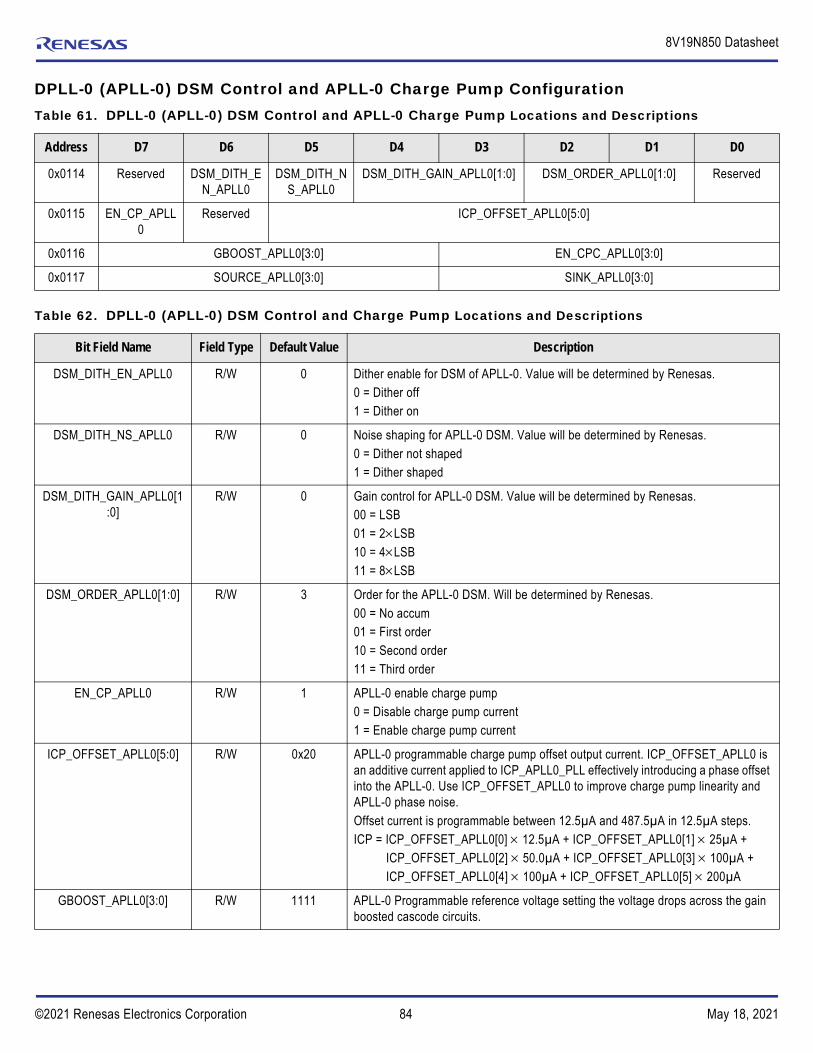
84©2021 Renesas Electronics Corporation May 18, 2021
8V19N850 Datasheet
DPLL-0 (APLL-0) DSM Control and APLL-0 Charge Pump Configuration Table 61. DPLL-0 (APLL-0) DSM Control and APLL-0 Charge Pump Locations and Descriptions
Address D7 D6 D5 D4 D3 D2 D1 D0
0x0114 Reserved DSM_DITH_EN_APLL0
DSM_DITH_NS_APLL0
DSM_DITH_GAIN_APLL0[1:0] DSM_ORDER_APLL0[1:0] Reserved
0x0115 EN_CP_APLL0
Reserved ICP_OFFSET_APLL0[5:0]
0x0116 GBOOST_APLL0[3:0] EN_CPC_APLL0[3:0]
0x0117 SOURCE_APLL0[3:0] SINK_APLL0[3:0]
Table 62. DPLL-0 (APLL-0) DSM Control and Charge Pump Locations and Descriptions
Bit Field Name Field Type Default Value Description
DSM_DITH_EN_APLL0 R/W 0 Dither enable for DSM of APLL-0. Value will be determined by Renesas.0 = Dither off1 = Dither on
DSM_DITH_NS_APLL0 R/W 0 Noise shaping for APLL-0 DSM. Value will be determined by Renesas.0 = Dither not shaped1 = Dither shaped
DSM_DITH_GAIN_APLL0[1:0]
R/W 0 Gain control for APLL-0 DSM. Value will be determined by Renesas.00 = LSB01 = 2LSB10 = 4LSB11 = 8LSB
DSM_ORDER_APLL0[1:0] R/W 3 Order for the APLL-0 DSM. Will be determined by Renesas.00 = No accum01 = First order10 = Second order11 = Third order
EN_CP_APLL0 R/W 1 APLL-0 enable charge pump0 = Disable charge pump current1 = Enable charge pump current
ICP_OFFSET_APLL0[5:0] R/W 0x20 APLL-0 programmable charge pump offset output current. ICP_OFFSET_APLL0 is an additive current applied to ICP_APLL0_PLL effectively introducing a phase offset into the APLL-0. Use ICP_OFFSET_APLL0 to improve charge pump linearity and APLL-0 phase noise.Offset current is programmable between 12.5µA and 487.5µA in 12.5µA steps. ICP = ICP_OFFSET_APLL0[0] 12.5µA + ICP_OFFSET_APLL0[1] 25µA +
ICP_OFFSET_APLL0[2] 50.0µA + ICP_OFFSET_APLL0[3] 100µA + ICP_OFFSET_APLL0[4] 100µA + ICP_OFFSET_APLL0[5] 200µA
GBOOST_APLL0[3:0] R/W 1111 APLL-0 Programmable reference voltage setting the voltage drops across the gain boosted cascode circuits.
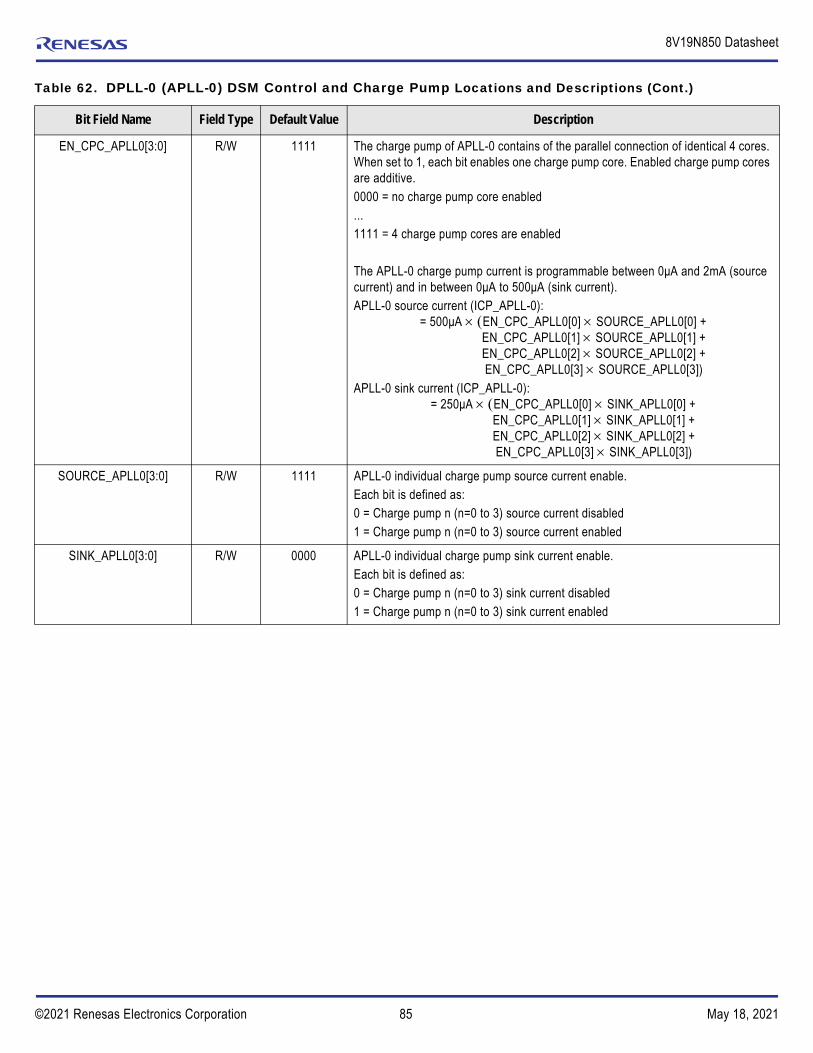
85©2021 Renesas Electronics Corporation May 18, 2021
8V19N850 Datasheet
EN_CPC_APLL0[3:0] R/W 1111 The charge pump of APLL-0 contains of the parallel connection of identical 4 cores. When set to 1, each bit enables one charge pump core. Enabled charge pump cores are additive. 0000 = no charge pump core enabled...1111 = 4 charge pump cores are enabled
The APLL-0 charge pump current is programmable between 0μA and 2mA (source current) and in between 0μA to 500μA (sink current).APLL-0 source current (ICP_APLL-0):
= 500μA EN_CPC_APLL0[0] SOURCE_APLL0[0] + EN_CPC_APLL0[1] SOURCE_APLL0[1] +EN_CPC_APLL0[2] SOURCE_APLL0[2] +EN_CPC_APLL0[3] SOURCE_APLL0[3])
APLL-0 sink current (ICP_APLL-0):= 250μA EN_CPC_APLL0[0] SINK_APLL0[0] +
EN_CPC_APLL0[1] SINK_APLL0[1] +EN_CPC_APLL0[2] SINK_APLL0[2] +EN_CPC_APLL0[3] SINK_APLL0[3])
SOURCE_APLL0[3:0] R/W 1111 APLL-0 individual charge pump source current enable. Each bit is defined as:0 = Charge pump n (n=0 to 3) source current disabled1 = Charge pump n (n=0 to 3) source current enabled
SINK_APLL0[3:0] R/W 0000 APLL-0 individual charge pump sink current enable. Each bit is defined as:0 = Charge pump n (n=0 to 3) sink current disabled1 = Charge pump n (n=0 to 3) sink current enabled
Table 62. DPLL-0 (APLL-0) DSM Control and Charge Pump Locations and Descriptions (Cont.)
Bit Field Name Field Type Default Value Description

86©2021 Renesas Electronics Corporation May 18, 2021
8V19N850 Datasheet
DPLL-0 Feedback Divider M0Table 63. DPLL-0 Feedback Divider M0 Register Locations
Address D7 D6 D5 D4 D3 D2 D1 D0
0x0118 M0_NUM_DPLL0[7:0]
0x0119 M0_NUM_DPLL0[15:8]
0x011A M0_NUM_DPLL0[23:16]
0x011C M0_DEN_DPLL0[7:0]
0x011D M0_DEN_DPLL0[15:8]
0x011E M0_DEN_DPLL0[23:16]
Table 64. DPLL-0 Feedback Divider M0 Register Descriptions
Bit Field Name Field Type Default Value Description
M0_NUM_DPLL0[23:0] R/W 0x000 Numerator portion of the fractional feedback divider of DPLL-0 for input clock 0 (CLK_0), (binary coding)
M0_DEN_DPLL0[23:0] R/W 0x800000 Denumerator portion of the fractional feedback divider of DPLL-0 for input clock 0 (CLK_0), (binary coding)

87©2021 Renesas Electronics Corporation May 18, 2021
8V19N850 Datasheet
DPLL-0 Frequency ControlTable 65. DPLL-0 Frequency Control Register Locations
Address D7 D6 D5 D4 D3 D2 D1 D0
0x0120 REF_SEL_MODE_DPLL0[1:0] REF_MAN_SEL_DPLL0
FB_SEL_DPLL0
REF_PRIORITY_DPLL0
REVERTIVE_EN_DPLL0
HITLESS_EN_DPLL0
TIE_CLR_DPLL0
Table 66. DPLL-0 Frequency Control Register Descriptions
Bit Field Name Field Type Default Value Description
REF_SEL_MODE_DPLL0[1:0] R/W 01 Reference Selection for DPLL-000 = Pin selection, follow CLK_n_SEL[1:0] through GPIO pins01 = Manual selection, follow ref_man_select_cnfg10 = Auto selection, select based on CLK_n qualities and priorities11 = Same as 00
REF_MAN_SEL_DPLL0 R/W 0 Selection of the DPLL-0 reference to TDC0 = CLK_01 = CLK_1
FB_SEL_DPLL0 R/W 0 Selection of the DPLL-0 feedback clock0 = DPLL-0 feedback divider1 = CLK_1 When this bit is set to 1, the phase detector can be used to measure two input clocks. In this case DPLL-0 should be manually set to select CLK-0. It can also be used for external loopback by connecting one of the DPLL-0 output to CLK_1.
REF_PRIORITY_DPLL0 R/W 0 This bit sets the priority of the clock0 = CLK_0 higher priority1 = CLK_1 higher priority
REVERTIVE_EN_DPLL0 R/W 0 This bit sets the revertive and non-revertive reference switching0 = Non-revertive1 = Revertive
HITLESS_EN_DPLL0 R/W 0 This bit enable/disable hitless reference switching0 = Disable1 = Enable
TIE_CLR_DPLL0 WC 0 If TIE_CLR_DPLL0 is set to 1, then the stored phase error is cleared, and DPLL0 output phase will align to the input reference. It is self-cleared.

88©2021 Renesas Electronics Corporation May 18, 2021
8V19N850 Datasheet
DPLL-0 Lock Timer
DPLL-0 Hitless Switch
Table 67. DPLL-0 Lock Timer Register Locations
Address D7 D6 D5 D4 D3 D2 D1 D0
0x0121 DPLL0_LOCK_TIMER[7:0]
0x0122 DPLL0_LOCK_TIMER[15:8]
Table 68. DPLL-0 Lock Timer Register Descriptions
Bit Field Name Field Type Default Value Description
DPLL0_LOCK_TIMER[15:0] R/W 0x00FF 16-bit unsignedLock timer = LOCK_TIMER_DPLL0[15:0]2msIf phase error is within the lock_threshold for the time set in this register, DPLL-0 declares lock
Table 69. DPLL-0 Hitless Switch Bit Field Locations
Address D7 D6 D5 D4 D3 D2 D1 D0
0x0123 HITLESS_BW_SHIFT_DPLL0[4:0] HITLESS_AVG_DPLL0[2:0]
Table 70. DPLL-0 Mode Control Bit Descriptions
Bit Field Name Field Type Default Value Description
HITLESS_BW_SHIFT_DPLL0[4:0]
R/W 0x0E DPLL-0 hitless switch, the bandwidth shift value
HITLESS_AVG_DPLL0[2:0] R/W 5 DPLL-0 hitless switch, the phase offset is averaged for 2^hitless_avg cycles of the (new) input clock

89©2021 Renesas Electronics Corporation May 18, 2021
8V19N850 Datasheet
DPLL-0 Mode ControlTable 71. DPLL-0 Mode Control Bit Field Locations
Address D7 D6 D5 D4 D3 D2 D1 D0
0x0124 PH_STS_SELECT_DPLL0
WRITE_PHASE_EN_DPLL
0
WRITE_FREQUENCY_EN
_DPLL0
Reserved Reserved DPLL_STATE_DPLL0[2:0]
0x0125 FILTER_STS_SELECT_DPLL0[1:0]
SYSCOMBO_MODE_EN_D
PLL0
COMBO_MODE_EN_DPLL
0
Reserved Reserved Reserved WRITE_TIMER_TRIG_DPL
L0
0x0126 Reserved FREQ_ON_TIMEOUT
FAIL_HOLD_DPLL0
DIRECT_WRITE_MODE_D
PLL0
Table 72. DPLL-0 Mode Control Bit Descriptions
Bit Field Name Field Type Default Value Description
PH_STS_SELECT_DPLL0 R/W 0 Selects source of the phase status register0 = From decimator1= From TDC
WRITE_PHASE_EN_DPLL0 R/W 0 This bit programs the device in write phase mode.0 = Normal DPLL mode, TDC phase get in to DPLL-01 = Write_phase mode enable
WRITE_FREQUENCY_EN_DPLL0
R/W 0 This bit programs the device in write frequency mode.0 = Normal DPLL-0 mode1 = Write_frequency mode enable, set FCW to the value set in register WRITE_FREQUENCY_CNFG
DPLL_STATE_DPLL0[2:0] R/W 5 DPLL-0 state Configuration:000 = Freerun001 = Lock acquisition010 = Lock011 = Holdover100 = Lock recovery101 = Auto state machine (freerun/acq1/lock/holdover/acq2)Others = Freerun
FILTER_STS_SELECT_DPLL0[1:0]
R/W 0 Selects source of the filter status register00 = Integrator10 = Proportional + integrator01 = Holdover value11 = fcw
SYSCOMBO_MODE_EN_DPLL0
R/W 0 Enable SYS-DPLL combo mode (add frequency control word from SysDPLL)0 = Disable1 = Enable syscombo mode

90©2021 Renesas Electronics Corporation May 18, 2021
8V19N850 Datasheet
COMBO_MODE_EN_DPLL0 R/W 0 Combo mode enable/disableEnable frequency control word from DPLL-10 = Disable1 = Enable
WRITE_TIMER_TRIG_DPLL0
WC 0 Write 1 to this bit will start the write_timer. This bit is self clear
FREQ_ON_TIMEOUT R/W 0 When the write timer expires, the value that is set in the DCO can be either the holdover value or the DCO can be set to zero. If FREQ_ON_TIMEOUT is zero, then when the write timer expires, the holdover value will be used and it is dependent on the holdover stateIf FREQ_ON_TIMEOUT is 1, then when the write timer expires, the DCO value is set to zero.
FAIL_HOLD_DPLL0 R/W 1 fail_hold0 = If the DPLL is programmed in lock acquisition, or lock recovery, or locked/normal state, and if the input clock fails, then the DPLL will stay in the programmed state (Lock acquisition, or Lock recovery, or Locked/normal state).1 = If the DPLL is programmed in lock acquisition, or Lock recovery, or Locked/Normal state, and if the input clock fails, then the DPLL will go to holdover state.
DIRECT_WRITE_MODE_DPLL0
R/W 1 direct_write_mode:0 = Write_phase and write_frequency active after write_timer is triggered and inactive when time out1 = Write_phase and write_frequency active right after being written, write_timer is not involved in this mode.
Table 72. DPLL-0 Mode Control Bit Descriptions (Cont.)
Bit Field Name Field Type Default Value Description

91©2021 Renesas Electronics Corporation May 18, 2021
8V19N850 Datasheet
DPLL-0 Phase Offset, Write Phase and FrequencyTable 73. DPLL-0 Phase Offset, Write Phase and Frequency Bit Field Locations
Address D7 D6 D5 D4 D3 D2 D1 D0
0x0127 PHASE_OFFSET_DPLL0[7:0]
0x0128 PHASE_OFFSET_DPLL0[15:8]
0x0129 PHASE_OFFSET_DPLL0[23:16]
0x012A PHASE_OFFSET_DPLL0[31:24]
0x012B Reserved PHASE_OFFSET_DPLL0[35:32]
0x012C WRITE_PHASE_DPLL0[7:0]
0x012D WRITE_PHASE_DPLL0[15:8]
0x012E WRITE_PHASE_DPLL0[23:16]
0x012F WRITE_PHASE_DPLL0[31:24]
0x0130 WRITE_FREQUENCY_DPLL0[7:0]
0x0131 WRITE_FREQUENCY_DPLL0[15:8]
0x0132 WRITE_FREQUENCY_DPLL0[23:16]
0x0133 WRITE_FREQUENCY_DPLL0[31:24]
0x0134 WRITE_FREQUENCY_DPLL0[39:32]
0x0135 Reserved WRITE_FREQUENCY_DPLL0[41:40]
0x0136 WRITE_TIMER_DPLL0[7:0]
0x0137 WRITE_TIMER_DPLL0[15:8]
Table 74. DPLL-0 Phase Offset, Write Phase and Frequency Bit Field Descriptions
Bit Field Name Field Type Default Value Description
PHASE_OFFSET_DPLL0[35:0]
R/W 0 Phase offset to adjust the phase offset between the feedback and clock input.36-bit 2's complementLSB = 1 TDC step, which is TSYSAPLL_VCO / 62 (period of the SYS-APLL VCO divided by 62)
WRITE_PHASE_DPLL0[31:0] R/W 0 In write phase mode, set the phase through this register. Write phase bits[31:0].32-bit 2's complementLSB = 1 TDC step, which is TSYSAPLL_VCO / 62 (period of the SYS-APLL VCO divided by 62)

92©2021 Renesas Electronics Corporation May 18, 2021
8V19N850 Datasheet
DPLL-0 Reference State
WRITE_FREQUENCY_DPLL0[41:0]
R/W 0 In write frequency mode, set DCO frequency through this register. Write frequency bits[41:0].42-bit 2's complementLSB = 2-53
max=±244ppm
WRITE_TIMER_DPLL0[15:0] R/W 0 This timer sets the total time that WRITE_PHASE_DPLL0 or WRITE_FREQUENCY_DPLL0 takes effect. 16-bit, unsignedThese bits set the total time to a multiple of 125us. When the write timer expires, the value that is set in the DCO can be either the holdover value or the DCO can be set to zero depending on the setting of FREQ_ON_TIMEOUT bit.
Table 75. DPLL-0 Reference State Bit Field Locations and Descriptions
Address D7 D6 D5 D4 D3 D2 D1 D0
0x0138 Reserved WRITE_TIMER_ACTIVE_S
TS_DPLL0
CURRENT_REF_STS_DPLL0[1:0]
LOCK_STS_DPLL0
DPLL_STATE_STS_DPLL0[2:0]
0x0139 FILTER_STS_DPLL0[7:0]
0x013A FILTER_STS_DPLL0[15:8]
0x013B FILTER_STS_DPLL0[23:16]
0x013C FILTER_STS_DPLL0[31:24]
0x013D FILTER_STS_DPLL0[39:32]
0x013E FILTER_STS_DPLL0[47:40]
0x013F PHASE_STS_DPLL0[7:0]
0x0140 PHASE_STS_DPLL0[15:8]
0x0141 PHASE_STS_DPLL0[23:16]
0x0142 PHASE_STS_DPLL0[31:24]
0x0143 Reserved PHASE_STS_DPLL0[35:32]
Table 74. DPLL-0 Phase Offset, Write Phase and Frequency Bit Field Descriptions (Cont.)
Bit Field Name Field Type Default Value Description

93©2021 Renesas Electronics Corporation May 18, 2021
8V19N850 Datasheet
Table 76. DPLL-0 Reference State Bit Field Locations and Descriptions
Bit Field Name Field Type Default Value Description
WRITE_TIMER_ACTIVE_STS_DPLL0
R/O 0 Indicate write timer active0 = Time out1 = Not time out (indicates write_phase/write_freqeuncy is in process)
CURRENT_REF_STS_DPLL0[1:0]
R/O 0 Indicate current selected ref00 = CLK-001 = CLK-1Others = No ref selected
LOCK_STS_DPLL0 R/O 0 dpll lock status0 = Unlock1 = Locked
DPLL_STATE_STS_DPLL0[2:0]
R/O 0 dpll states:000 = Freerun001 = Lock acquisition010 = Normal lock011 = Holdover100 = Lock recovery
FILTER_STS_DPLL0[47:0] R/O 0 DPLL-0 filter status controlled by FILTER_STS_SELECT_DPLL0. 48-bit 2's complementLSB = 2-53
Report DPLL-0 filter status according to FILTER_STS_SELECT_DPLL0.
PHASE_STS_DPLL0[35:0] R/O 0 DPLL-0 phase status.36-bit 2's complementLSB = TSYSAPLL_VCO / 62Current phase data from decimator or TDC selected by PH_STS_SELECT_DPLL0 bit.

94©2021 Renesas Electronics Corporation May 18, 2021
8V19N850 Datasheet
DPLL-0 Lock Threshold, Lock Timer, BandwidthTable 77. DPLL-0 Lock Threshold, Lock Timer, Bandwidth Bit Field Locations and Descriptions
Address D7 D6 D5 D4 D3 D2 D1 D0
0x0144 LOCK_THRESHOLD_DPLL0[7:0]
0x0145 LOCK_THRESHOLD_DPLL0[15:8]
0x0146 FREQ_SNAP_SLOPE_DPLL0[7:0]
0x0147 AA_BW_SHIFT_DPLL0[4:0] AA_BW_MULT_DPLL0[2:0]
0x0148 NORMAL_BW_SHIFT_DPLL0[4:0] NORMAL_BW_MULT_DPLL0[2:0]
0x0149 Reserved NORMAL_DAMPING_SHIFT_DPLL0[2:0] NORMAL_DAMPING_MULT_DPLL0[2:0]
0x014A ACQ_BW_SHIFT_DPLL0[4:0] ACQ_BW_MULT_DPLL0[2:0]
0x014B Reserved ACQ_DAMPING_SHIFT_DPLL0[2:0] ACQ_DAMPING_MULT_DPLL0[2:0]
Table 78. DPLL-0 Lock Threshold, Lock Timer, Bandwidth Bit Field Locations and Descriptions
Bit Field Name Field Type Default Value Description
LOCK_THRESHOLD_DPLL0[15:0]
R/W 0x155 DPLL-0 lock detector threshold16-bit, unsignedLSB = TSYSAPLL_VCO / 62
FREQ_SNAP_SLOPE_DPLL0[7:0]
R/W 0x20 Frequency snap slope limit8-bit unsignedLSB of 2-408000 106 ppm/s.If these bits are set to 0, then the frequency snap slope limit is unlimited.
AA_BW_SHIFT_DPLL0[4:0] R/W 0xF Anti alias shift.Anti aliasing filter bandwidth = coef/(2π)where,coe = 2-(18-AA_BW_SHIFT_DPLL0) AA_BW_MULT_DPLL0/8f = fb frequencyif AA_BW_MULT_DPLL0=0, then the anti aliasing filter is bypassed
AA_BW_MULT_DPLL0[2:0] R/W 4 Anti alias multi. See AA_BW_SHIFT_DPLL0[4:0] description.
NORMAL_BW_SHIFT_DPLL0[4:0]
R/W 0x12 Normal bandwidth shift. Normal bandwidth shift and mult must be < 24 for stabilityBW = (KTDC KPEC KP) / 2πWhere:
KTDC = 1 / TDC_STEP
TDC_STEP = TSYSAPLL_VCO / 62 (in ps)KPEC = 27
KP = (NORMAL_BW_SHIFT_DPLL0/4) 2(NORMAL_BW_SHIFT_DPLL0-53)
NORMAL_BW_MULT_DPLL0[2:0]
R/W 4 Normal bandwidth mult. See NORMAL_BW_SHIFT_DPLL0[4:0] description.

95©2021 Renesas Electronics Corporation May 18, 2021
8V19N850 Datasheet
NORMAL_DAMPING_SHIFT_DPLL0[2:0]
R/W 4 Normal damping shiftThe estimation for Gpeak is:Gpeak(dB) = 0.0122(NORMAL_DAMPING_SHIFT_DPLL0-1)NORMAL_DAMPING_MULT_DPLL0/4 --- assuming filter update rate is 562.5kHz. if update rate doubles, then Gpeak doubles
NORMAL_DAMPING_MULT_DPLL0[2:0]
R/W 5 Normal damping mult. See NORMAL_DAMPING_SHIFT_DPLL0[2:0] description.
ACQ_BW_SHIFT_DPLL0[4:0] R/W 0x16 Acquire bandwidth shift. Acquire bandwidth shift and mult: <24 for stability, BW = (KTDC KPEC KP) / 2πWhere:
KTDC = 1e12 / TDC_STEP
TDC_STEP = TSYSAPLL_VCO / 62 (in ps)KPEC = 27
KP = (ACQ_BW_MULT_DPLL0/4) 2(ACQ_BW_SHIFT_DPLL0-53)
ACQ_BW_MULT_DPLL0[2:0] R/W 4 Acquire bandwidth mult. See ACQ_BW_SHIFT_DPLL0[4:0] description.
ACQ_DAMPING_SHIFT_DPLL0[2:0]
R/W 4 Acquire damping bandwidth shift The estimation for Gpeak is:Gpeak(dB) = 0.0122(ACQ_DAMPING_SHIFT_DPLL0-1)ACQ_DAMPING_MULT_DPLL0/4 --- assuming filter update rate is 562.5kHz. if update rate doubles, then Gpeak doubles
ACQ_DAMPING_MULT_DPLL0[2:0]
R/W 5 Acquire damping bandwidth multSee ACQ_DAMPING_SHIFT_DPLL0[4:0] description.
Table 78. DPLL-0 Lock Threshold, Lock Timer, Bandwidth Bit Field Locations and Descriptions (Cont.)
Bit Field Name Field Type Default Value Description

96©2021 Renesas Electronics Corporation May 18, 2021
8V19N850 Datasheet
DPLL-0 Phase Slope LimitingTable 79. DPLL-0 Phase Slope Limiting Bit Field Locations
Address D7 D6 D5 D4 D3 D2 D1 D0
0x014C PHASE_SLOPE_LIMIT_DPLL0[7:0]
0x014D PHASE_SLOPE_LIMIT_DPLL0[15:8]
0x014E PHASE_SLOPE_LIMIT_DPLL0[23:16]
0x014F Reserved PHASE_SLOPE_LIMIT_DPLL0[30:24]
0x0150 INTEGRATOR_LIMIT_DPLL0[7:0]
0x0151 INTEGRATOR_LIMIT_DPLL0[15:8]
0x0152 INTEGRATOR_LIMIT_DPLL0[23:16]
0x0153 Reserved INTEGRATOR_LIMIT_DPLL0[30:24]
Table 80. DPLL-0 Phase Slope Limiting Bit Field Descriptions
Bit Field Name Field Type Default Value Description
PHASE_SLOPE_LIMIT_DPLL0[30:0]
R/W 0x7FFFFFFF DPLL phase slope limit configuration. These bits are used to limit the phase slope of the DPLL output. 31-bit unsignedLSB = 2-37106 (us/s)
INTEGRATOR_LIMIT_DPLL0[30:0]
R/W 0x7FFFFFFF These bits are used to program the pull-in range of the DPLL.31-bit, unsignedLSB = 2-43106 (ppm) max = 2312-43106 = 244ppm

97©2021 Renesas Electronics Corporation May 18, 2021
8V19N850 Datasheet
DPLL-0 Holdover, Phase Error Compensation (PEC)Table 81. DPLL-0 Holdover, Phase Error Compensation Bit Field Locations and Descriptions
Address D7 D6 D5 D4 D3 D2 D1 D0
0x0154 HOLDOVER_BW_SHIFT_DPLL0[4:0] HOLDOVER_MULT_DPLL0[2:0]
0x0155 HOLDOVER_MODE_DPLL0[1:0]
HOLDOVER_HISTORY_DPLL0[5:0]
0x0156 HOLDOVER_VALUE_DPLL0[7:0]
0x0157 HOLDOVER_VALUE_DPLL0[15:8]
0x0158 HOLDOVER_VALUE_DPLL0[23:16]
0x0159 HOLDOVER_VALUE_DPLL0[31:24]
0x015A HOLDOVER_VALUE_DPLL0[39:32]
0x015B Reserved HOLDOVER_VALUE_DPLL0[41:40]
0x015C PEC_CLK0_CORR_DPLL0[7:0]
0x015D Reserved PEC_CLK0_CORR_DPLL0[13:8]
0x015E PEC_CLK1_CORR_DPLL0[7:0]
0x015F Reserved PEC_CLK1_CORR_DPLL0[13:8]
Table 82. DPLL-0 Holdover, Phase Error Compensation Bit Field Locations and Descriptions
Bit Field Name Field Type Default Value Description
HOLDOVER_BW_SHIFT_DPLL0[4:0]
R/W 8 DPLL-0 Holdover filter bandwidth shift.Holdover filter bandwidth = coe f/(2π) wherecoe = 2-(33-HOLDOVER_BW_SHIFT_DPLL0) HOLDOVER_MULT_DPLL0 / 4f = DPLL-0 update rateIf coe = 0, the filter is bypassed
HOLDOVER_MULT_DPLL0[2:0]
R/W 4 DPLL-0 Holdover filter bandwidth multiplierSee HOLDOVER_BW_SHIFT_DPLL0[4:0] description.
HOLDOVER_MODE_DPLL0[1:0]
R/W 0 00 = Instantaneous01 = History instantaneous10 = Manual holdover11 = History averaged
HOLDOVER_HISTORY_DPLL0[5:0]
R/W 0 Set holdover history from 1s to 64s0 = Averaged value of 1s before1 = Averaged value of 2s before…63 = Averaged value of 64s before
HOLDOVER_VALUE_DPLL0[41:0]
R/W 0 The value for manual holdover frequency. 42-bit, 2's complementLSB = 2-53
Max = ±244ppm
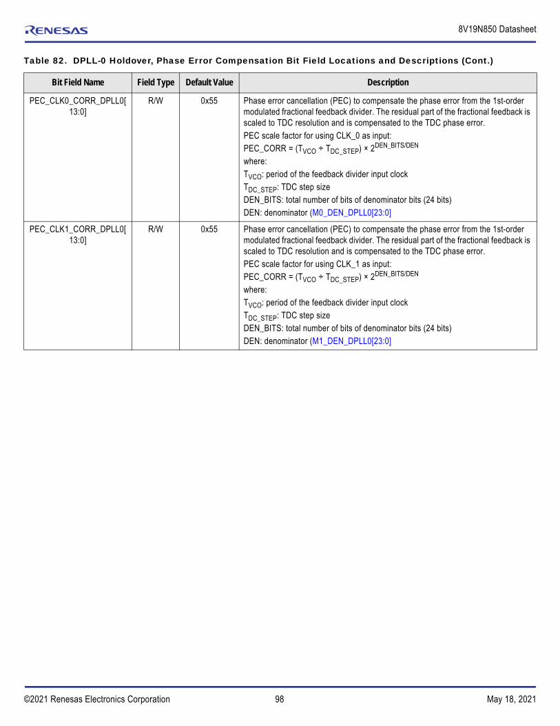
98©2021 Renesas Electronics Corporation May 18, 2021
8V19N850 Datasheet
PEC_CLK0_CORR_DPLL0[13:0]
R/W 0x55 Phase error cancellation (PEC) to compensate the phase error from the 1st-order modulated fractional feedback divider. The residual part of the fractional feedback is scaled to TDC resolution and is compensated to the TDC phase error.PEC scale factor for using CLK_0 as input:PEC_CORR = (TVCO ÷ TDC_STEP) × 2DEN_BITS/DEN
where:TVCO: period of the feedback divider input clock TDC_STEP: TDC step sizeDEN_BITS: total number of bits of denominator bits (24 bits)DEN: denominator (M0_DEN_DPLL0[23:0]
PEC_CLK1_CORR_DPLL0[13:0]
R/W 0x55 Phase error cancellation (PEC) to compensate the phase error from the 1st-order modulated fractional feedback divider. The residual part of the fractional feedback is scaled to TDC resolution and is compensated to the TDC phase error.PEC scale factor for using CLK_1 as input:PEC_CORR = (TVCO ÷ TDC_STEP) × 2DEN_BITS/DEN
where:TVCO: period of the feedback divider input clock TDC_STEP: TDC step sizeDEN_BITS: total number of bits of denominator bits (24 bits)DEN: denominator (M1_DEN_DPLL0[23:0]
Table 82. DPLL-0 Holdover, Phase Error Compensation Bit Field Locations and Descriptions (Cont.)
Bit Field Name Field Type Default Value Description
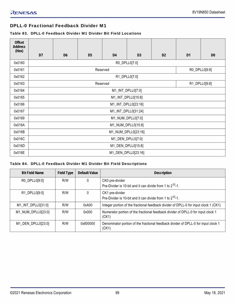
99©2021 Renesas Electronics Corporation May 18, 2021
8V19N850 Datasheet
DPLL-0 Fractional Feedback Divider M1Table 83. DPLL-0 Feedback Divider M1 Divider Bit Field Locations
Offset Address
(Hex)D7 D6 D5 D4 D3 D2 D1 D0
0x0160 R0_DPLL0[7:0]
0x0161 Reserved R0_DPLL0[9:8]
0x0162 R1_DPLL0[7:0]
0x0163 Reserved R1_DPLL0[9:8]
0x0164 M1_INT_DPLL0[7:0]
0x0165 M1_INT_DPLL0[15:8]
0x0166 M1_INT_DPLL0[23:16]
0x0167 M1_INT_DPLL0[31:24]
0x0169 M1_NUM_DPLL0[7:0]
0x016A M1_NUM_DPLL0[15:8]
0x016B M1_NUM_DPLL0[23:16]
0x016C M1_DEN_DPLL0[7:0]
0x016D M1_DEN_DPLL0[15:8]
0x016E M1_DEN_DPLL0[23:16]
Table 84. DPLL-0 Feedback Divider M1 Divider Bit Field Descriptions
Bit Field Name Field Type Default Value Description
R0_DPLL0[9:0] R/W 0 CK0 pre-dividerPre-Divider is 10-bit and it can divide from 1 to 210-1.
R1_DPLL0[9:0] R/W 0 CK1 pre-dividerPre-Divider is 10-bit and it can divide from 1 to 210-1.
M1_INT_DPLL0[31:0] R/W 0xA00 Integer portion of the fractional feedback divider of DPLL-0 for input clock 1 (CK1)
M1_NUM_DPLL0[23:0] R/W 0x000 Numerator portion of the fractional feedback divider of DPLL-0 for input clock 1 (CK1)
M1_DEN_DPLL0[23:0] R/W 0x800000 Denominator portion of the fractional feedback divider of DPLL-0 for input clock 1 (CK1)

100©2021 Renesas Electronics Corporation May 18, 2021
8V19N850 Datasheet
DPLL-1 (APLL-1) Frequency ConfigurationTable 85. DPLL-1 (APLL-1) Frequency Configuration Field Locations
Address D7 D6 D5 D4 D3 D2 D1 D0
0x0180 M_INT_APLL1[7:0]
0x0181 Reserved M_INT_APLL1[9:8]
0x0182 M0_INT_DPLL1[7:0]
0x0183 M0_INT_DPLL1[15:8]
0x0184 M0_INT_DPLL1[23:16]
0x0185 M0_INT_DPLL1[31:24]
0x0186 1 1 Reserved FB_SEL_DPLL1_RF
0x0187 PD_APLL1 PD_PFD_APLL1
PD_FB_APLL1
PD_FB_DPLL1
PD_P1 Reserved
0x0188 M_NUM_APLL1[7:0]
0x0189 M_NUM_APLL1[15:8]
0x018A M_NUM_APLL1[23:16]
0x018C M_DEN_APLL1[7:0]
0x018D M_DEN_APLL1[15:8]
0x018E M_DEN_APLL1[23:16]
0x0190 CAL_REF_APLL1[7:0]
0x0191 CAL_EN_APLL1
Reserved CAL_REF_APLL1[13:8]
0x0192 Reserved P1[6:0]
Table 86. DPLL-1 (APLL-1) Frequency Configuration Field Descriptions
Bit Field Name Field Type Default Value Description
M_INT_APLL1[9:0] R/W 0x028 Integer portion of the fractional feedback divider of APLL-1 (binary coding).
M0_INT_DPLL1[31:0 R/W 0xFBA Integer portion of the fractional feedback divider of DPLL-1 for input clock 0 (REF0), (binary coding)
FB_SEL_DPLL1_RF R/W 0 Feedback select for DPLL-1 fractional vs RF0 = Selects DPLL1 FRAC FB divider1 = Selects 2^N RF FB divider
PD_APLL1 R/W 0 Power down APLL-1 (except VCO of APLL-1)0 = Power up1 = Power down
PD_PFD_APLL1 R/W 0 Power down APLL-1 phase frequency detector0 = Power up1 = Power down
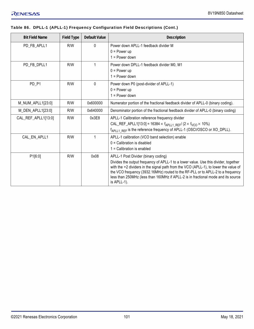
101©2021 Renesas Electronics Corporation May 18, 2021
8V19N850 Datasheet
PD_FB_APLL1 R/W 0 Power down APLL-1 feedback divider M0 = Power up1 = Power down
PD_FB_DPLL1 R/W 1 Power down DPLL-1 feedback divider M0, M10 = Power up1 = Power down
PD_P1 R/W 0 Power down P0 (post-divider of APLL-1)0 = Power up1 = Power down
M_NUM_APLL1[23:0] R/W 0x600000 Numerator portion of the fractional feedback divider of APLL-0 (binary coding).
M_DEN_APLL1[23:0] R/W 0x640000 Denominator portion of the fractional feedback divider of APLL-0 (binary coding)
CAL_REF_APLL1[13:0] R/W 0x3E8 APLL-1 Calibration reference frequency dividerCAL_REF_APLL1[13:0] = 16384 fAPLL1_REF/ (2 fVCO 10%)fAPLL1_REF is the reference frequency of APLL-1 (OSCI/OSCO or XO_DPLL).
CAL_EN_APLL1 R/W 1 APLL-1 calibration (VCO band selection) enable0 = Calibration is disabled1 = Calibration is enabled
P1[6:0] R/W 0x08 APLL-1 Post Divider (binary coding)Divides the output frequency of APLL-1 to a lower value. Use this divider, together with the ÷2 dividers in the signal path from the VCO (APLL-1), to lower the value of the VCO frequency (3932.16MHz) routed to the RF-PLL or to APLL-2 to a frequency less than 250MHz (less than 160MHz if APLL-2 is in fractional mode and its source is APLL-1).
Table 86. DPLL-1 (APLL-1) Frequency Configuration Field Descriptions (Cont.)
Bit Field Name Field Type Default Value Description

102©2021 Renesas Electronics Corporation May 18, 2021
8V19N850 Datasheet
DPLL-1 (APLL-1) DSM Control and APLL-1 Charge Pump Configuration Table 87. DPLL-1 (APLL-1) DSM Control and APLL-1 Charge Pump Locations and Descriptions
Address D7 D6 D5 D4 D3 D2 D1 D0
0x0194 Reserved DSM_DITH_EN_APLL1
DSM_DITH_NS_APLL1
DSM_DITH_GAIN_APLL1[1:0] DSM_ORDER_APLL1[1:0] Reserved
0x0195 EN_CP_APLL1
Reserved ICP_OFFSET_APLL1[5:0]
0x0196 GBOOST_APLL1[3:0] EN_CPC_APLL1[3:0]
0x0197 SOURCE_APLL1[3:0] SINK_APLL1[3:0]
Table 88. DPLL-1 (APLL-1) DSM Control and Charge Pump Locations and Descriptions
Bit Field Name Field Type Default Value Description
DSM_DITH_EN_APLL1 R/W 0 Dither enable for DSM of APLL-1. Value will be determined by Renesas.0 = Dither off1 = Dither on
DSM_DITH_NS_APLL1 R/W 0 Noise shaping for APLL-1 DSM. Value will be determined by Renesas.0 = Dither not shaped1 = Dither shaped
DSM_DITH_GAIN_APLL1[1:0]
R/W 0 Gain control for APLL-1 DSM. Value will be determined by Renesas.00 = LSB01 = 2LSB10 = 4LSB11 = 8LSB
DSM_ORDER_APLL1[1:0] R/W 3 Order for the APLL-1 DSM. Will be determined by Renesas.00 = No accum01 = First order10 = Second order11 = Third order
EN_CP_APLL1 R/W 1 APLL-1 enable charge pump0 = Disable charge pump current1 = Enable charge pump current
ICP_OFFSET_APLL1[5:0] R/W 0x20 APLL-1 programmable charge pump offset output current. ICP_OFFSET_APLL1 is an additive current applied to ICP_APLL1 effectively introducing a phase offset into the APLL-1. Use ICP_OFFSET_APLL1 to improve charge pump linearity and APLL-1 phase noise.Offset current is programmable between 12.5µA and 487.5µA in 12.5µA steps. ICP = ICP_OFFSET_APLL1[0] 12.5µA + ICP_OFFSET_APLL1[1] 25µA +
ICP_OFFSET_APLL1[2] 50.0µA + ICP_OFFSET_APLL1[3] 100µA + ICP_OFFSET_APLL1[4] 100µA + ICP_OFFSET_APLL1[5] 200µA
GBOOST_APLL1[3:0] R/W 0xF APLL-1 Programmable reference voltage setting the voltage drops across the gain boosted cascode circuits. Value will be determined by Renesas.

103©2021 Renesas Electronics Corporation May 18, 2021
8V19N850 Datasheet
EN_CPC_APLL1[3:0] R/W 0xF The charge pump of APLL-1 contains of the parallel connection of identical 4 cores. When set to 1, each bit enables one charge pump core. Enabled charge pump cores are additive. 0000 = no charge pump core enabled...1111 = 4 charge pump cores are enabledThe APLL-1 charge pump current is programmable between 0μA and 2mA (source current) and in between 0μA to 500μA (sink current).
APLL-1 source current (ICP_APLL-1):= 500μA EN_CPC_APLL1[0] SOURCE_APLL1[0] +
EN_CPC_APLL1[1] SOURCE_APLL1[1] +EN_CPC_APLL1[2] SOURCE_APLL1[2] +EN_CPC_APLL1[3] SOURCE_APLL1[3])
APLL-1 sink current (ICP_APLL-1):= 250μA EN_CPC_APLL1[0] SINK_APLL1[0] +
EN_CPC_APLL1[1] SINK_APLL1[1] +EN_CPC_APLL1[2] SINK_APLL1[2] +EN_CPC_APLL1[3] SINK_APLL1[3])
SOURCE_APLL1[3:0] R/W 0xF APLL-1 individual charge pump source current enable. Each bit is defined as:0 = Charge pump n (n=0 to 3) source current disabled1 = Charge pump n (n=0 to 3) source current enabled
SINK_APLL1[3:0] R/W 0 APLL-1 individual charge pump sink current enable. Each bit is defined as:0 = Charge pump n (n=0 to 3) sink current disabled1 = Charge pump n (n=0 to 3) sink current enabled
Table 89. DPLL-1 Frequency Control Bit Locations
Address D7 D6 D5 D4 D3 D2 D1 D0
0x0198 M0_NUM_DPLL1[7:0]
0x0199 M0_NUM_DPLL1[15:8]
0x019A M0_NUM_DPLL1[23:16]
0x019C M0_DEN_DPLL1[7:0]
0x019D M0_DEN_DPLL1[15:8]
0x019E M0_DEN_DPLL1[23:16]
0x01A0 REF_SEL_MODE_DPLL1[1:0] REF_MAN_SEL_DPLL1
FB_SEL_DPLL1
REF_PRIORITY_DPLL1
REVERTIVE_EN_DPLL1
HITLESS_EN_DPLL1
TIE_CLR_DPLL1
Table 88. DPLL-1 (APLL-1) DSM Control and Charge Pump Locations and Descriptions (Cont.)
Bit Field Name Field Type Default Value Description

104©2021 Renesas Electronics Corporation May 18, 2021
8V19N850 Datasheet
Table 90. DPLL-1 Frequency Control Bit Field Descriptions
Bit Field Name Field Type Default Value Description
M0_NUM_DPLL1[23:0] R/W 0x33F000 Numerator portion of the fractional feedback divider of DPLL-1 for input clock 0 (REF0), (binary coding)
M0_DEN_DPLL1[23:0] R/W 0x61A800 Denominator portion of the fractional feedback divider of DPLL-1 for input clock 0(REF0), (binary coding)
REF_SEL_MODE_DPLL1[1:0]
R/W 1 Reference Selection for DPLL-100 = Pin selection, follow CLK_n_SEL[1:0] through GPIO pins01 = Manual selection, follow REF_MAN_SEL_DPLL110 = Auto selection, select based on CLK_n qualities and priorities11 = Same as 00
REF_MAN_SEL_DPLL1 R/W 1 Selection of the DPLL-1 reference to TDC0 = CLK_01 = CLK_1
FB_SEL_DPLL1 R/W 0 Selection of the DPLL-1 feedback clock0 = Selects per FB_SEL_DPLL1_RF1 = CLK_1 When this bit is set to 1, the phase detector can be used to measure two input clocks. In this case DPLL-1 should be manually set to select CLK-0. It can also be used for external loopback by connecting one of the DPLL-1 output to CLK_1.
REF_PRIORITY_DPLL1 R/W 0 This bit sets the priority of the clock.0 = CLK_0 higher priority1 = CLK_1 higher priority
REVERTIVE_EN_DPLL1 R/W 0 This bit sets the revertive and non-revertive reference switching.0 = Non-revertive1 = Revertive
HITLESS_EN_DPLL1 R/W 0 This bit enable/disable hitless reference switching.0 = Disable1 = Enable
TIE_CLR_DPLL1 WC 0 If TIE_CLR_DPLL1 is set to 1, then the stored phase error is cleared, and DPLL1 output phase will align to the input reference. It is self-cleared.
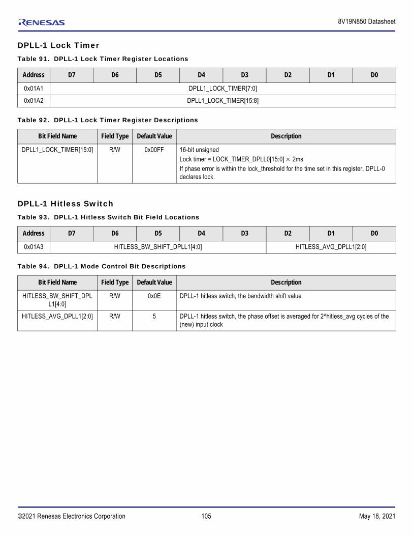
105©2021 Renesas Electronics Corporation May 18, 2021
8V19N850 Datasheet
DPLL-1 Lock Timer
DPLL-1 Hitless Switch
Table 91. DPLL-1 Lock Timer Register Locations
Address D7 D6 D5 D4 D3 D2 D1 D0
0x01A1 DPLL1_LOCK_TIMER[7:0]
0x01A2 DPLL1_LOCK_TIMER[15:8]
Table 92. DPLL-1 Lock Timer Register Descriptions
Bit Field Name Field Type Default Value Description
DPLL1_LOCK_TIMER[15:0] R/W 0x00FF 16-bit unsignedLock timer = LOCK_TIMER_DPLL0[15:0]2msIf phase error is within the lock_threshold for the time set in this register, DPLL-0 declares lock.
Table 93. DPLL-1 Hitless Switch Bit Field Locations
Address D7 D6 D5 D4 D3 D2 D1 D0
0x01A3 HITLESS_BW_SHIFT_DPLL1[4:0] HITLESS_AVG_DPLL1[2:0]
Table 94. DPLL-1 Mode Control Bit Descriptions
Bit Field Name Field Type Default Value Description
HITLESS_BW_SHIFT_DPLL1[4:0]
R/W 0x0E DPLL-1 hitless switch, the bandwidth shift value
HITLESS_AVG_DPLL1[2:0] R/W 5 DPLL-1 hitless switch, the phase offset is averaged for 2^hitless_avg cycles of the (new) input clock

106©2021 Renesas Electronics Corporation May 18, 2021
8V19N850 Datasheet
DPLL-1 Mode ControlTable 95. DPLL-1 Mode Control Bit Field Locations
Address D7 D6 D5 D4 D3 D2 D1 D0
0x01A4 PH_STS_SELECT_DPLL1
WRITE_PHASE_EN_DPLL
1
WRITE_FREQUENCY_EN
_DPLL1
Reserved Reserved DPLL_STATE_DPLL1[2:0]
0x01A5 FILTER_STS_SELECT_DPLL1[1:0]
SYSCOMBO_MODE_EN_D
PLL1
COMBO_MODE_EN_DPLL
1
Reserved Reserved Reserved WRITE_TIMER_TRIG_DPL
L1
0x01A6 Reserved FREQ_ON_TIMEOUT
FAIL_HOLD_DPLL1
DIRECT_WRITE_MODE_D
PLL1
Table 96. DPLL-1 Mode Control Bit Field Descriptions
Bit Field Name Field Type Default Value Description
PH_STS_SELECT_DPLL1 R/W 0 Selects source of the phase status register.1 = From TDC0 = From decimator
WRITE_PHASE_EN_DPLL1 R/W 0 This bit programs DPLL-1 in write phase mode.0 = Normal DPLL mode, TDC phase get in to DPLL-11 = Write_phase mode enable
WRITE_FREQUENCY_EN_DPLL1
R/W 0 This bit programs DPLL-1 in write frequency mode.0 = Normal DPLL mode1 = Write_frequency mode enable, set FCW to the value set in register
WRITE_FREQUENCY_CNFG
DPLL_STATE_DPLL1[2:0] R/W 5 DPLL-1 state Configuration:000 = Freerun001 = Lock acquisition010 = Lock011 = Holdover100 = Lock recovery101 = Auto state machine (freerun/acq1/lock/holdover/acq2)Others = Freerun
FILTER_STS_SELECT_DPLL1[1:0]
R/W 0 Selects source of the filter status register00 = Integrator10 = Proportional + integrator01= Holdover value11= fcw
SYSCOMBO_MODE_EN_DPLL1
R/W 0 Enable SYS-DPLL combo mode (add frequency control word from SysDPLL)0 = Disable1 = Enable syscombo mode

107©2021 Renesas Electronics Corporation May 18, 2021
8V19N850 Datasheet
COMBO_MODE_EN_DPLL1
R/W 0 Combo mode enable/disableEnable frequency control word from DPLL-00 = Disable1 = Enable
WRITE_TIMER_TRIG_DPLL1
WC 0 Write 1 to this bit will start the write_timer. This bit is self clear
FREQ_ON_TIMEOUT R/W 0 When the write timer expires, the value that is set in the DCO can be either the holdover value or the DCO can be set to zero. If FREQ_ON_TIMEOUT is zero, then when the write timer expires, the holdover value will be used and it is dependent on the holdover stateIf FREQ_ON_TIMEOUT is 1, then when the write timer expires, the DCO value is set to zero.
FAIL_HOLD_DPLL1 R/W 1 fail_hold0 = If the DPLL is programmed in lock acquisition, or Lock recovery, or Locked/Normal state, and if the input clock fails, then the DPLL will stay in the programmed state (Lock acquisition, or Lock recovery, or Locked/normal state).1 = If the DPLL is programmed in lock acquisition, or Lock recovery, or Locked/Normal state, and if the input clock fails, then the DPLL will go to holdover state.
DIRECT_WRITE_MODE_DPLL1
R/W 1 direct_write_mode:0 = Write_phase and write_frequency active after write_timer is triggered and inactive when time out1 = Write_phase and write_frequency active right after being written, write_timer is not involved in this mode.
Table 96. DPLL-1 Mode Control Bit Field Descriptions (Cont.)
Bit Field Name Field Type Default Value Description

108©2021 Renesas Electronics Corporation May 18, 2021
8V19N850 Datasheet
DPLL-1 Phase Offset, Write Phase and FrequencyTable 97. DPLL-1 Phase Offset, Write Phase and Frequency Bit Field Locations
Address D7 D6 D5 D4 D3 D2 D1 D0
0x01A7 PHASE_OFFSET_DPLL1[7:0]
0x01A8 PHASE_OFFSET_DPLL1[15:8]
0x01A9 PHASE_OFFSET_DPLL1[23:16]
0x01AA PHASE_OFFSET_DPLL1[31:24]
0x01AB Reserved PHASE_OFFSET_DPLL1[35:32]
0x01AC WRITE_PHASE_DPLL1[7:0]
0x01AD WRITE_PHASE_DPLL1[15:8]
0x01AE WRITE_PHASE_DPLL1[23:16]
0x01AF WRITE_PHASE_DPLL1[31:24]
0x01B0 WRITE_FREQUENCY_DPLL1[7:0]
0x01B1 WRITE_FREQUENCY_DPLL1[15:8]
0x01B2 WRITE_FREQUENCY_DPLL1[23:16]
0x01B3 WRITE_FREQUENCY_DPLL1[31:24]
0x01B4 WRITE_FREQUENCY_DPLL1[39:32]
0x01B5 Reserved WRITE_FREQUENCY_DPLL1[41:40]
0x01B6 WRITE_TIMER_DPLL1[7:0]
0x01B7 WRITE_TIMER_DPLL1[15:8]
Table 98. DPLL-1 Phase Offset, Write Phase and Frequency Bit Field Descriptions
Bit Field Name Field Type Default Value Description
PHASE_OFFSET_DPLL1[35:0]
R/W 0 Phase offset to adjust the phase offset between the feedback and clock input.36-bit 2's complementLSB = 1 TDC step, which is TSYSAPLL_VCO / 62
WRITE_PHASE_DPLL1[31:0]
R/W 0 In write phase mode, set the phase through this register. Write phase bits[31:0]32-bit 2's complementLSB = 1 TDC step, which is TSYSAPLL_VCO / 62

109©2021 Renesas Electronics Corporation May 18, 2021
8V19N850 Datasheet
WRITE_FREQUENCY_DPLL1[41:0]
R/W 0 In write frequency mode, set DCO frequency through this register. Write frequency bits[41:0]42-bit 2's complementLSB = 2-53
Max = ±244ppm
WRITE_TIMER_DPLL1[15:0] R/W 0 This timer sets the total time that the write_phase or write_frequency takes effect. If time out, then '0' is written in the loop.16-bit, unsignedThese bits set the total time to a multiple of 125us.When the write timer expires, the value that is set in the DCO can be either the holdover value or the DCO can be set to zero depending on the setting of FREQ_ON_TIMEOUT bit.
Table 98. DPLL-1 Phase Offset, Write Phase and Frequency Bit Field Descriptions (Cont.)
Bit Field Name Field Type Default Value Description

110©2021 Renesas Electronics Corporation May 18, 2021
8V19N850 Datasheet
DPLL-1 Reference StateTable 99. DPLL-1 Reference State Bit Field Locations and Descriptions
Address D7 D6 D5 D4 D3 D2 D1 D0
0x01B8 Reserved WRITE_TIMER_ACTIVE_S
TS_DPLL1
CURRENT_REF_STS_DPLL1[1:0]
LOCK_STS_DPLL1
DPLL_STATE_STS_DPLL1[2:0]
0x01B9 FILTER_STS_DPLL1[7:0]
0x01BA FILTER_STS_DPLL1[15:8]
0x01BB FILTER_STS_DPLL1[23:16]
0x01BC FILTER_STS_DPLL1[31:24]
0x01BD FILTER_STS_DPLL1[39:32]
0x01BE FILTER_STS_DPLL1[47:40]
0x01BF PHASE_STS_DPLL1[7:0]
0x01C0 PHASE_STS_DPLL1[15:8]
0x01C1 PHASE_STS_DPLL1[23:16]
0x01C2 PHASE_STS_DPLL1[31:24]
0x01C3 Reserved PHASE_STS_DPLL1[35:32]
Table 100. DPLL-1 Reference State Bit Field Locations and Descriptions
Bit Field Name Field Type Default Value Description
WRITE_TIMER_ACTIVE_STS_DPLL1
R/O 0 Indicates write timer active0 = Time out1 = Not time out
CURRENT_REF_STS_DPLL1[1:0]
R/O 0 Indicates current selected ref00 = Ref001 = Ref1Others = No ref selected
LOCK_STS_DPLL1 R/O 0 DPLL lock sts0 = Unlock1 = Locked
DPLL_STATE_STS_DPLL1[2:0]
R/O 0 DPLL states.000 = Freerun001 = Lock acquisition010 = Normal lock011 = Holdover100 = Lock recovery

111©2021 Renesas Electronics Corporation May 18, 2021
8V19N850 Datasheet
FILTER_STS_DPLL1[47:0] R/O 0 DPLL-1 filter status controlled by FILTER_STS_SELECT_DPLL1. 48-bit 2's complementLSB = 2-53
Report DPLL-1 filter status according to FILTER_STS_SELECT_DPLL1.
PHASE_STS_DPLL1[35:0] R/O 0 DPLL-1 phase status.36-bit 2's complementLSB = TSYSAPLL_VCO / 62Current phase data from decimator or TDC selected by PH_STS_SELECT_DPLL1 bit.
Table 100. DPLL-1 Reference State Bit Field Locations and Descriptions (Cont.)
Bit Field Name Field Type Default Value Description

112©2021 Renesas Electronics Corporation May 18, 2021
8V19N850 Datasheet
DPLL-1 Lock Threshold, Lock Timer, BandwidthTable 101. DPLL-1 Lock Threshold, Lock Timer, Bandwidth Bit Field Locations and Descriptions
Address D7 D6 D5 D4 D3 D2 D1 D0
0x01C4 LOCK_THRESHOLD_DPLL1[7:0]
0x01C5 LOCK_THRESHOLD_DPLL1[15:8]
0x01C6 FREQ_SNAP_SLOPE_DPLL1[7:0]
0x01C7 AA_BW_SHIFT_DPLL1[4:0] AA_BW_MULT_DPLL1[2:0]
0x01C8 NORMAL_BW_SHIFT_DPLL1[4:0] NORMAL_BW_MULT_DPLL1[2:0]
0x01C9 Reserved NORMAL_DAMPING_SHIFT_DPLL1[2:0] NORMAL_DAMPING_MULT_DPLL1[2:0]
0x01CA ACQ_BW_SHIFT_DPLL1[4:0] ACQ_BW_MULT_DPLL1[2:0]
0x01CB Reserved ACQ_DAMPING_SHIFT_DPLL1[2:0] ACQ_DAMPING_MULT_DPLL1[2:0]
Table 102. DPLL-1 Lock Threshold, Lock Timer, Bandwidth Bit Field Locations and Descriptions
Bit Field Name Field Type Default Value Description
LOCK_THRESHOLD_DPLL1[15:0]
R/W 0x0155 DPLL-1 lock detector threshold16-bit, unsignedLSB = TSYSAPLL_VCO / 62
FREQ_SNAP_SLOPE_DPLL1[7:0]
R/W 0x20 Frequency snap slope limit8-bit unsignedLSB of 2-40 8000 106 ppm/s.If these bits are set to 0, then the frequency snap slope limit is unlimited.
AA_BW_SHIFT_DPLL1[4:0] R/W 0x0A Anti alias shift.Anti aliasing filter bandwidth = coef/(2π)where,coe = 2-(18-AA_BW_SHIFT_DPLL1)AA_BW_MULT_DPLL1/8f = fb frequencyif AA_BW_MULT_DPLL1=0, then the anti aliasing filter is bypassed
AA_BW_MULT_DPLL1[2:0] R/W 4 Anti alias multi. See AA_BW_SHIFT_DPLL1[4:0] description.
NORMAL_BW_SHIFT_DPLL1[4:0]
R/W 0x0D Normal bandwidth shift. Normal bandwidth shift and mult must be < 24 for stabilityBW = (KTDC KPEC KP) / 2πWhere:
KTDC = 1/TDC_STEP
TDC_STEP = TSYSAPLL_VCO / 62 (in ps)KPEC = 27
KP = (NORMAL_BW_SHIFT_DPLL1/4) 2(NORMAL_BW_SHIFT_DPLL1-53)
NORMAL_BW_MULT_DPLL1[2:0]
R/W 4 Normal bandwidth mult. See NORMAL_BW_SHIFT_DPLL1[4:0] description.
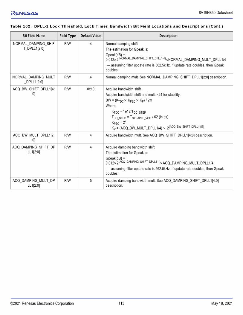
113©2021 Renesas Electronics Corporation May 18, 2021
8V19N850 Datasheet
NORMAL_DAMPING_SHIFT_DPLL1[2:0]
R/W 4 Normal damping shiftThe estimation for Gpeak is:Gpeak(dB) = 0.0122(NORMAL_DAMPING_SHIFT_DPLL1-1)NORMAL_DAMPING_MULT_DPLL1/4 --- assuming filter update rate is 562.5kHz. if update rate doubles, then Gpeak doubles
NORMAL_DAMPING_MULT_DPLL1[2:0]
R/W 4 Normal damping mult. See NORMAL_DAMPING_SHIFT_DPLL1[2:0] description.
ACQ_BW_SHIFT_DPLL1[4:0]
R/W 0x10 Acquire bandwidth shift. Acquire bandwidth shift and mult: <24 for stability, BW = (KTDC KPEC KP) / 2πWhere:
KTDC = 1e12/TDC_STEP
TDC_STEP = TSYSAPLL_VCO / 62 (in ps)KPEC = 27
KP = (ACQ_BW_MULT_DPLL1/4)2(ACQ_BW_SHIFT_DPLL1-53)
ACQ_BW_MULT_DPLL1[2:0]
R/W 4 Acquire bandwidth mult. See ACQ_BW_SHIFT_DPLL1[4:0] description.
ACQ_DAMPING_SHIFT_DPLL1[2:0]
R/W 4 Acquire damping bandwidth shift The estimation for Gpeak is:Gpeak(dB) = 0.0122(ACQ_DAMPING_SHIFT_DPLL1-1)ACQ_DAMPING_MULT_DPLL1/4 --- assuming filter update rate is 562.5kHz. if update rate doubles, then Gpeak doubles
ACQ_DAMPING_MULT_DPLL1[2:0]
R/W 5 Acquire damping bandwidth mult. See ACQ_DAMPING_SHIFT_DPLL1[4:0] description.
Table 102. DPLL-1 Lock Threshold, Lock Timer, Bandwidth Bit Field Locations and Descriptions (Cont.)
Bit Field Name Field Type Default Value Description

114©2021 Renesas Electronics Corporation May 18, 2021
8V19N850 Datasheet
DPLL-1 Phase Slope LimitingTable 103. DPLL-1 Phase Slope Limiting Bit Field Locations
Address D7 D6 D5 D4 D3 D2 D1 D0
0x01CC PHASE_SLOPE_LIMIT_DPLL1[7:0]
0x01CD PHASE_SLOPE_LIMIT_DPLL1[15:8]
0x01CE PHASE_SLOPE_LIMIT_DPLL1[23:16]
0x01CF Reserved PHASE_SLOPE_LIMIT_DPLL1[30:24]
0x01D0 INTEGRATOR_LIMIT_DPLL1[7:0]
0x01D1 INTEGRATOR_LIMIT_DPLL1[15:8]
0x01D2 INTEGRATOR_LIMIT_DPLL1[23:16]
0x01D3 Reserved INTEGRATOR_LIMIT_DPLL1[30:24]
Table 104. DPLL-1 Phase Slope Limiting Bit Field Descriptions
Bit Field Name Field Type Default Value Description
PHASE_SLOPE_LIMIT_DPLL1[30:0]
R/W 0x7FFFFFFF DPLL phase slope limit configuration. These bits are used to limit the phase slope of the DPLL output. 31-bit unsignedLSB = 2-37 106 (us/s)
INTEGRATOR_LIMIT_DPLL1[30:0]
R/W 0x7FFFFFFF These bits are used to program the pull-in range of the DPLL.31-bit, unsignedLSB = 2-43 106 (ppm) Max = 231 2-43 106 = 244ppm

115©2021 Renesas Electronics Corporation May 18, 2021
8V19N850 Datasheet
DPLL-1 Holdover, Phase Error Compensation (PEC)Table 105. DPLL-1 Holdover, Phase Error Compensation Bit Field Locations and Descriptions
Address D7 D6 D5 D4 D3 D2 D1 D0
0x01D4 HOLDOVER_BW_SHIFT_DPLL1[4:0] HOLDOVER_MULT_DPLL1[2:0]
0x01D5 HOLDOVER_MODE_DPLL1[1:0]
HOLDOVER_HISTORY_DPLL1[5:0]
0x01D6 HOLDOVER_VALUE_DPLL1[7:0]
0x01D7 HOLDOVER_VALUE_DPLL1[15:8]
0x01D8 HOLDOVER_VALUE_DPLL1[23:16]
0x01D9 HOLDOVER_VALUE_DPLL1[31:24]
0x01DA HOLDOVER_VALUE_DPLL1[39:32]
0x01DB Reserved HOLDOVER_VALUE_DPLL1[41:40]
0x01DC PEC_CLK0_CORR_DPLL1[7:0]
0x01DD Reserved PEC_CLK0_CORR_DPLL1[13:8]
0x01DE PEC_CLK1_CORR_DPLL1[7:0]
0x01DF Reserved PEC_CLK1_CORR_DPLL1[13:0]
Table 106. DPLL-1 Holdover, Phase Error Compensation Bit Field Locations and Descriptions
Bit Field a Name Field Type Default Value Description
HOLDOVER_BW_SHIFT_DPLL1[4:0]
R/W 8 DPLL-1 Holdover filter bandwidth shift.Holdover filter bandwidth = coe f/(2π) wherecoe = 2-(33-HOLDOVER_BW_SHIFT_DPLL1) HOLDOVER_MULT_DPLL1 / 4f = DPLL-1 update rateIf coe = 0, the filter is bypassed.
HOLDOVER_MULT_DPLL1[2:0]
R/W 4 DPLL-1 Holdover filter bandwidth mult. See HOLDOVER_BW_SHIFT_DPLL1[4:0] description.
HOLDOVER_MODE_DPLL1[1:0]
R/W 0 00 = Instantaneous01 = History instantaneous10 = Manual holdover11 = History averaged

116©2021 Renesas Electronics Corporation May 18, 2021
8V19N850 Datasheet
HOLDOVER_HISTORY_DPLL1[5:0]
R/W 0 Set holdover history from 1s to 64s0 = Averaged value of 1s before1 = Averaged value of 2s before…63= averaged value of 64s before
HOLDOVER_VALUE_DPLL1[41:0]
R/W 0 The value for manual holdover frequency. 42-bit, 2's complementLSB = 2-53
Max = ±244ppm
PEC_CLK0_CORR_DPLL1[13:0]
R/W 0x23 Phase error cancellation (PEC) to compensate the phase error from the 1st-order modulated fractional feedback divider. The residual part of the fractional feedback is scaled to TDC resolution and is compensated to the TDC phase error.PEC scale factor for using CLK_0 as input:PEC_CORR = (TVCO ÷ TDC_STEP) × 2DEN_BITS/DEN
where: TVCO: period of the feedback divider input clock TDC_STEP: TDC step size DEN_BITS: total number of bits of denominator bits (24 bits) DEN: denominator (M0_DEN_DPLL1[23:0]
PEC_CLK1_CORR_DPLL1[13:0]
R/W 0x23 Phase error cancellation (PEC) to compensate the phase error from the 1st-order modulated fractional feedback divider. The residual part of the fractional feedback is scaled to TDC resolution and is compensated to the TDC phase error.PEC scale factor for using CLK_1 as input:PEC_CORR = (TVCO ÷ TDC_STEP) × 2DEN_BITS/DEN
where: TVCO: period of the feedback divider input clock TDC_STEP: TDC step size DEN_BITS: total number of bits of denominator bits (24 bits) DEN: denominator (M1_DEN_DPLL1[23:0]
Table 106. DPLL-1 Holdover, Phase Error Compensation Bit Field Locations and Descriptions (Cont.)
Bit Field a Name Field Type Default Value Description

117©2021 Renesas Electronics Corporation May 18, 2021
8V19N850 Datasheet
DPLL-1 Fractional Feedback Divider M1Table 107. DPLL-1 Feedback Divider M1 Divider Bit Field Locations
Offset Address
(Hex) D7 D6 D5 D4 D3 D2 D1 D0
0x01E0 R0_DPLL1[7:0]
0x01E1 Reserved R0_DPLL1[9:8]
0x01E2 R1_DPLL1[7:0]
0x01E3 Reserved R1_DPLL1[9:8]
0x01E4 M1_INT_DPLL1[7:0]
0x01E5 M1_INT_DPLL1[15:8]
0x01E6 M1_INT_DPLL1[23:16]
0x01E7 M1_INT_DPLL1[31:24]
0x01E9 M1_NUM_DPLL1[7:0]
0x01EA M1_NUM_DPLL1[15:8]
0x01EB M1_NUM_DPLL1[23:16]
0x01EC M1_DEN_DPLL1[7:0]
0x01ED M1_DEN_DPLL1[15:8]
0x01EE M1_DEN_DPLL1[23:16]
Table 108. DPLL-1 Feedback Divider M1 Divider Bit Field Descriptions
Bit Field Name Field Type Default Value Description
R0_DPLL1[9:0] R/W 0 CK0 pre-dividerPre-Divider is 14-bit and it can divide from 1 to 210-1.
R1_DPLL1[9:0] R/W 0 CK1 pre-dividerPre-Divider is 14-bit and it can divide from 1 to 210-1.
M1_INT_DPLL1[31:0] R/W 0xFBA Integer portion of the fractional feedback divider of DPLL-1 for input clock 1 (REF1), (binary coding)
M1_NUM_DPLL1[23:0] R/W 0x33F000 Integer portion of the fractional feedback divider of DPLL-1 for input clock 1 (REF1), (binary coding)
M1_DEN_DPLL1[23:0] R/W 0x61A800 Integer portion of the fractional feedback divider of DPLL-1 for input clock 1 (REF1), (binary coding)

118©2021 Renesas Electronics Corporation May 18, 2021
8V19N850 Datasheet
APLL-2 Configuration RegistersTable 109. APLL-2 Configuration Bit Field Locations
Address D7 D6 D5 D4 D3 D2 D1 D0
0x0200 M_INT_APLL2[7:0]
0x0201 DSM_EN_APLL2
SYNTH_MODE
Reserved Reserved
0x0202 CAL_REF_APLL2[7:0]
0x0203 CAL_EN_APLL2
Reserved CAL_REF_APLL2[13:8]
0x0204 M_NUM_APLL2[7:0]
0x0205 M_NUM_APLL2[15:8]
0x0206 M_NUM_APLL2[23:16]
0x0208 M_DEN_APLL2[7:0]
0x0209 M_DEN_APLL2[15:8]
0x020A M_DEN_APLL2[23:16]
0x020C Reserved DSM_DITH_EN_APLL2
DSM_DITH_NS_APLL2
DSM_DITH_GAIN_APLL2[1:0] DSM_ORDER_APLL2[1:0] Reserved
0x020D EN_CP_APLL2
Reserved ICP_OFFSET_APLL2[5:0]
0x020E GBOOST_APLL2[3:0] EN_CPC_APLL2[3:0]
0x020F SOURCE_APLL2[3:0] SINK_APLL2[3:0]
0x0210 PD_APLL2 PD_PFD_APLL2
PD_M_APLL2 RSEL_APLL2 Reserved
Table 110. APLL-2 Configuration Bit Field Locations
Bit Field Name Field Type Default Value Description
M_INT_APLL2[7:0] R/W 0x31 Integer portion of the APLL-2 PLL feedback divider.
SYNTH_MODE R/W 1 APLL-2 Mode of operation0 = APLL-2 is used as DCO for the SYS-DPLL1 = APLL-2 is used as an independent synthesizer for output frequency generation. In this mode, SYS-DPLL operation is not possible
DSM_EN_APLL2 R/W 1 APLL-2 DSM (Delta-Sigma Modulator) enable. Determines the operational mode of the APLL-2 feedback divider. Must use fractional mode for use of APLL-2 as DCO of the SYS-DPLL.0 = Integer mode (lower power, better spurious performance)
fVCO_APLL2 = fAPLL2_IN M_INT_APLL2. Use for lowest spurious.
1 = Fractional mode:fVCO_APLL2 = fAPLL2_IN [M_INT_APLL2 + (M_NUM_APLL2 ÷ M_DEN_APLL2)]

119©2021 Renesas Electronics Corporation May 18, 2021
8V19N850 Datasheet
CAL_REF_APLL2[13:0] R/W 0x675 APLL-2 VCO auto-calibration frequency reference dividerCAL_REF_APLL2[13:0] = 16384 fAPLL2_REF/ (2 fVCO 10%)If APLL-2 is used as synthesizer, fAPLL2_REF is the frequency from either APLL-0 or APLL-1, if APLL-2 is used as part of the SYS-DPLL, fAPLL2_REF is the crystal frequency.
CAL_EN_APLL2 R/W 0
Value: Disabled
APLL-2 VCO auto-calibration enable.During VCO calibration, the PLL selects a VCO band. Leave this setting at the default value (auto-calibration is enabled). In auto-calibration, also configure CAL_REF_APLL2[13:0].0 = APLL-2 VCO auto-calibration is disabled (default).1 = APLL-2 VCO auto-calibration is enabled
M_NUM_APLL2[23:0] R/W 0x430000 APLL-2 Numerator (NUM) of the APLL-2 DSM.Value range is 0x000000 to 0xFFFFFF. M_NUM_APLL2 < M_DEN_APLL2; APLL-2 should be a large value (as close as possible to 0xFFFFFF).Set DSM_EN_APLL2 = 1 to use the APLL-2 in fractional mode. See the DSM_EN_APLL2 description for operation.
M_DEN_APLL2[23:0] R/W 0x7D0000 APLL-2 Denominator (DEN) of the APLL-2 DSM.Value range is 0x000000 to 0xFFFFFF. Set M_NUM_APLL2 < M_DEN_APLL2.Set DSM_EN_APLL2 = 1 to use the APLL-2 in fractional mode. See the DSM_EN_APLL2 description for operation.
DSM_DITH_EN_APLL2 R/W 0 Dither enable for DSM of APLL-2. Value will be determined by Renesas.0 = Dither off1 = Dither on
DSM_DITH_NS_APLL2 R/W 0 Noise shaping for APLL-2 DSM. Value will be determined by Renesas.0 = Dither not shaped1 = Dither shaped
DSM_DITH_GAIN_APLL2[1:0]
R/W 00 Gain control for APLL-2 DSM. Value will be determined by Renesas.00 = LSB01 = 2LSB10 = 4LSB11 = 8LSB
DSM_ORDER_APLL2[1:0] R/W 11 Order for the APLL-2 DSM. Will be determined by Renesas.00 = No accum01 = First order10 = Second order11 = Third order
EN_CP_APLL2 R/W 1 APLL-2 enable charge pump0 = Disable charge pump current1 = Enable charge pump current
Table 110. APLL-2 Configuration Bit Field Locations (Cont.)
Bit Field Name Field Type Default Value Description
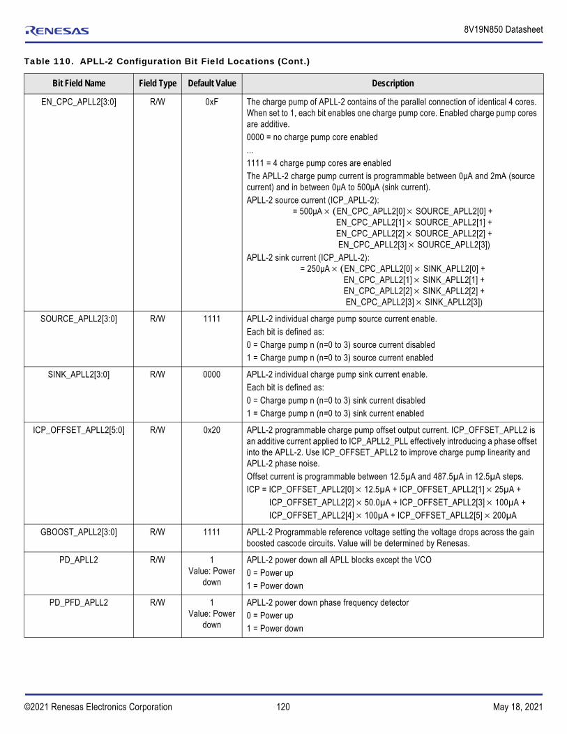
120©2021 Renesas Electronics Corporation May 18, 2021
8V19N850 Datasheet
EN_CPC_APLL2[3:0] R/W 0xF The charge pump of APLL-2 contains of the parallel connection of identical 4 cores. When set to 1, each bit enables one charge pump core. Enabled charge pump cores are additive. 0000 = no charge pump core enabled...1111 = 4 charge pump cores are enabledThe APLL-2 charge pump current is programmable between 0μA and 2mA (source current) and in between 0μA to 500μA (sink current).APLL-2 source current (ICP_APLL-2):
= 500μA EN_CPC_APLL2[0] SOURCE_APLL2[0] + EN_CPC_APLL2[1] SOURCE_APLL2[1] +EN_CPC_APLL2[2] SOURCE_APLL2[2] +EN_CPC_APLL2[3] SOURCE_APLL2[3])
APLL-2 sink current (ICP_APLL-2):= 250μA EN_CPC_APLL2[0] SINK_APLL2[0] +
EN_CPC_APLL2[1] SINK_APLL2[1] +EN_CPC_APLL2[2] SINK_APLL2[2] +EN_CPC_APLL2[3] SINK_APLL2[3])
SOURCE_APLL2[3:0] R/W 1111 APLL-2 individual charge pump source current enable. Each bit is defined as:0 = Charge pump n (n=0 to 3) source current disabled1 = Charge pump n (n=0 to 3) source current enabled
SINK_APLL2[3:0] R/W 0000 APLL-2 individual charge pump sink current enable. Each bit is defined as:0 = Charge pump n (n=0 to 3) sink current disabled1 = Charge pump n (n=0 to 3) sink current enabled
ICP_OFFSET_APLL2[5:0] R/W 0x20 APLL-2 programmable charge pump offset output current. ICP_OFFSET_APLL2 is an additive current applied to ICP_APLL2_PLL effectively introducing a phase offset into the APLL-2. Use ICP_OFFSET_APLL2 to improve charge pump linearity and APLL-2 phase noise.Offset current is programmable between 12.5µA and 487.5µA in 12.5µA steps. ICP = ICP_OFFSET_APLL2[0] 12.5µA + ICP_OFFSET_APLL2[1] 25µA +
ICP_OFFSET_APLL2[2] 50.0µA + ICP_OFFSET_APLL2[3] 100µA + ICP_OFFSET_APLL2[4] 100µA + ICP_OFFSET_APLL2[5] 200µA
GBOOST_APLL2[3:0] R/W 1111 APLL-2 Programmable reference voltage setting the voltage drops across the gain boosted cascode circuits. Value will be determined by Renesas.
PD_APLL2 R/W 1Value: Power
down
APLL-2 power down all APLL blocks except the VCO0 = Power up1 = Power down
PD_PFD_APLL2 R/W 1Value: Power
down
APLL-2 power down phase frequency detector0 = Power up1 = Power down
Table 110. APLL-2 Configuration Bit Field Locations (Cont.)
Bit Field Name Field Type Default Value Description
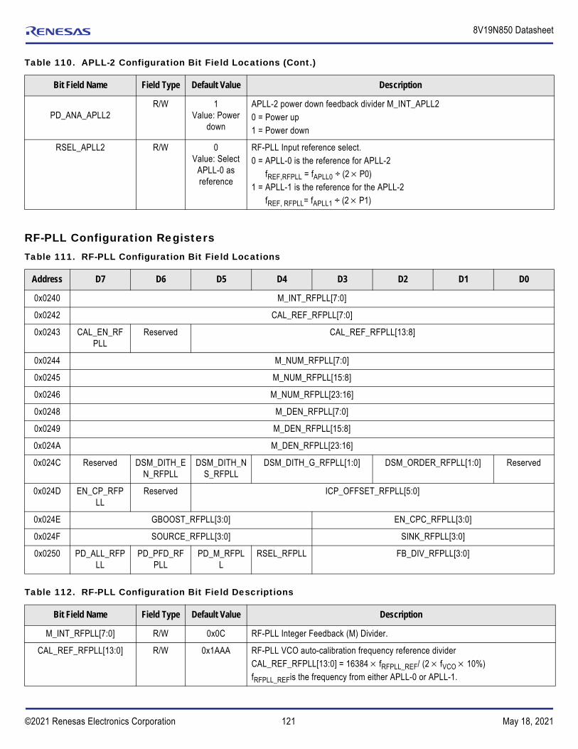
121©2021 Renesas Electronics Corporation May 18, 2021
8V19N850 Datasheet
RF-PLL Configuration Registers
PD_ANA_APLL2R/W 1
Value: Power down
APLL-2 power down feedback divider M_INT_APLL20 = Power up1 = Power down
RSEL_APLL2 R/W 0Value: Select
APLL-0 as reference
RF-PLL Input reference select.0 = APLL-0 is the reference for APLL-2
fREF,RFPLL = fAPLL0 ÷ (2 P0)1 = APLL-1 is the reference for the APLL-2
fREF, RFPLL= fAPLL1 ÷ (2 P1)
Table 111. RF-PLL Configuration Bit Field Locations
Address D7 D6 D5 D4 D3 D2 D1 D0
0x0240 M_INT_RFPLL[7:0]
0x0242 CAL_REF_RFPLL[7:0]
0x0243 CAL_EN_RFPLL
Reserved CAL_REF_RFPLL[13:8]
0x0244 M_NUM_RFPLL[7:0]
0x0245 M_NUM_RFPLL[15:8]
0x0246 M_NUM_RFPLL[23:16]
0x0248 M_DEN_RFPLL[7:0]
0x0249 M_DEN_RFPLL[15:8]
0x024A M_DEN_RFPLL[23:16]
0x024C Reserved DSM_DITH_EN_RFPLL
DSM_DITH_NS_RFPLL
DSM_DITH_G_RFPLL[1:0] DSM_ORDER_RFPLL[1:0] Reserved
0x024D EN_CP_RFPLL
Reserved ICP_OFFSET_RFPLL[5:0]
0x024E GBOOST_RFPLL[3:0] EN_CPC_RFPLL[3:0]
0x024F SOURCE_RFPLL[3:0] SINK_RFPLL[3:0]
0x0250 PD_ALL_RFPLL
PD_PFD_RFPLL
PD_M_RFPLL
RSEL_RFPLL FB_DIV_RFPLL[3:0]
Table 112. RF-PLL Configuration Bit Field Descriptions
Bit Field Name Field Type Default Value Description
M_INT_RFPLL[7:0] R/W 0x0C RF-PLL Integer Feedback (M) Divider.
CAL_REF_RFPLL[13:0] R/W 0x1AAA RF-PLL VCO auto-calibration frequency reference dividerCAL_REF_RFPLL[13:0] = 16384 fRFPLL_REF/ (2 fVCO 10%)fRFPLL_REFis the frequency from either APLL-0 or APLL-1.
Table 110. APLL-2 Configuration Bit Field Locations (Cont.)
Bit Field Name Field Type Default Value Description

122©2021 Renesas Electronics Corporation May 18, 2021
8V19N850 Datasheet
CAL_EN_RFPLL R/W 1
Value: Auto-Calibrati
on
RF-PLL VCO auto-calibration enable.During VCO calibration, the PLL selects a VCO band. Leave this setting at the default value (auto-calibration is enabled). In auto-calibration, also configure CAL_REF_RFPLL[13:0].0 = RF-PLL VCO auto-calibration is disabled1 = RF-PLL VCO auto-Calibration is enabled (default).
EN_CP_RFPLL R/W 1 RF-PLL enable charge pump0 = Disable charge pump current1 = Enable charge pump current
EN_CPC_RFPLL[3:0] R/W 1111 The charge pump of PLL-0 contains of the parallel connection of identical 4 cores. When set to 1, each bit enables one charge pump core. Enabled charge pump cores are additive. 0000 = No charge pump core enabled1000 = First charge pump core enabled, other three cores disabled...1111 = 4 charge pump cores are enabledThe RF_PLL charge pump current is programmable between 0μA and 2mA (source current) and in between 0μA to 500μA (sink current).RF_PLL source current (ICP_RF_PLL):
= 500μA EN_CPC_RFPLL[0] SOURCE_RFPLL[0] + EN_CPC_RFPLL[1] SOURCE_RFPLL[1] +EN_CPC_RFPLL[2] SOURCE_RFPLL[2] +EN_CPC_RFPLL[3] SOURCE_RFPLL[3])
RF_PLL sink current (ICP_RF_PLL):= 250μA EN_CPC_RFPLL[0] SINK_RFPLL[0] +
EN_CPC_RFPLL[1] SINK_RFPLL[1] +EN_CPC_RFPLL[2] SINK_RFPLL[2] +EN_CPC_RFPLL[3] SINK_RFPLL[3])
SOURCE_RFPLL[3:0] R/W 1111 RF-PLL individual charge pump source current enable. Each bit is defined as:0 = Charge pump core n (n=0 to 3) source current disabled1 = Charge pump core n (n=0 to 3) source current enabled
SINK_RFPLL[3:0] R/W 0000 RF-PLL individual charge pump sink current enable. Each bit is defined as:0 = Charge pump n (n=0 to 3) sink current disabled1 = Charge pump n (n=0 to 3) sink current enabled
ICP_OFFSET_RFPLL[5:0] R/W 100000
Value: 200µA
RF-PLL programmable charge pump offset output current. ICP_OFFSET_RF_PLL is an additive current applied to ICP_RF_PLL effectively introducing a phase offset into the RF-PLL. Use ICP_OFFSET_RF_PLL to improve charge pump linearity and RF-PLL phase noise.Offset current is programmable between 12.5µA and 487.5µA in 12.5µA steps. ICP = ICP_OFFSET_RPFLL[0] 12.5µA + ICP_OFFSET_RPFLL[1] 25µA +
ICP_OFFSET_RPFLL[2] 50.0µA + ICP_OFFSET_RPFLL[3] 100µA + ICP_OFFSET_RPFLL[4] 100µA + ICP_OFFSET_RPFLL[5] 200µA
Table 112. RF-PLL Configuration Bit Field Descriptions (Cont.)
Bit Field Name Field Type Default Value Description
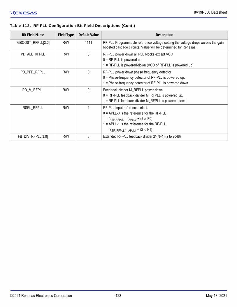
123©2021 Renesas Electronics Corporation May 18, 2021
8V19N850 Datasheet
GBOOST_RFPLL[3:0] R/W 1111 RF-PLL Programmable reference voltage setting the voltage drops across the gain boosted cascade circuits. Value will be determined by Renesas.
PD_ALL_RFPLL R/W 0 RF-PLL power down all PLL blocks except VCO0 = RF-PLL is powered up.1 = RF-PLL is powered-down (VCO of RF-PLL is powered up)
PD_PFD_RFPLL R/W 0 RF-PLL power down phase frequency detector0 = Phase-frequency detector of RF-PLL is powered up.1 = Phase-frequency detector of RF-PLL is powered down.
PD_M_RFPLL R/W 0 Feedback divider M_RFPLL power-down0 = RF-PLL feedback divider M_RFPLL is powered up.1 = RF-PLL feedback divider M_RFPLL is powered down.
RSEL_RFPLL R/W 1 RF-PLL Input reference select.0 = APLL-0 is the reference for the RF-PLL
fREF,RFPLL = fAPLL0 ÷ (2 P0)1 = APLL-1 is the reference for the RF-PLL
fREF, RFPLL= fAPLL1 ÷ (2 P1)
FB_DIV_RFPLL[3:0] R/W 6 Extended RF-PLL feedback divider 2^(N+1) (2 to 2048)
Table 112. RF-PLL Configuration Bit Field Descriptions (Cont.)
Bit Field Name Field Type Default Value Description

124©2021 Renesas Electronics Corporation May 18, 2021
8V19N850 Datasheet
SYSREF RegistersTable 113. SYSREF Bit Field Locations
Address D7 D6 D5 D4 D3 D2 D1 D0
0x288 Reserved N_SYNC[6:0]
0x289 PD_S Reserved SYSREF_AC
0x28A N_S[3:0] Reserved
0x28B SRPC[7:0]
0x28C REF_S[7:0]
0x28D REF_S[8] Reserved
0x28E PD_SYSREF Reserved SRG[2:0] SRO[1:0]
0x28F SRWC[7:0]
Table 114. SYSREF Bit Field Descriptions
Bit Field Name Field Type Default Value Description
N_SYNC[6:0] R/W 0011 010
Value: ÷24 (8 3)
SYSREF Frequency and SYSREF Synchronizer divider.This divider controls the release of SYSREF pulses at coincident QCLK_y clock edges. For SYSREF operation, set this divider value to a common multiple of the output channel clock divider values N_x that is greater than or equal to 12. For instance, if N_R0=÷2, N_R1=÷3 and N_R2=÷4 set the N_SYNC divider to ÷12. N_SYNC is a also a frequency divider for SYSREF, see N_S divider description.The value of the frequency divider is set by the product of N_SYNC[6:3] N_SYNC[2:0]N_SYNC[6:3] N_SYNC[2:0]
0000 = ÷10001 = ÷20010 = ÷40011 = ÷80100 = ÷160101 = ÷320110 = ÷640111 = ÷1281000 = ÷2561001 = ÷5121010 = ÷10241011 - 1111 = reserved
000 = ÷1001 = ÷2010 = ÷3011 = ÷4100 = ÷5101 - 111 = reserved
PD_S R/W 0 Power down SYSREF0 = All SYSREF functions are powered-up1 = All SYSREF functions are powered-down
SYSREF_AC R/W 0 SYSREF output voltage bias0 = QREF_r outputs are in a low/high state when nBIAS_r is set to 1 or during a SYSREF event (use for DC coupled outputs)1 = QREF_r outputs are in a cross-point biased state when nBIAS_r is set to 1 or during a SYSREF event (use for AC-coupled outputs).

125©2021 Renesas Electronics Corporation May 18, 2021
8V19N850 Datasheet
N_S[3:0] R/W 0110 N_S (together with N_SYNC) divides the RF-PLL frequency generating the SYSREF frequency for JESD204B operation.fSYSREF = fVCO_RF_PLL ÷ (N_S N_SYNC)0000 = ÷10001 = ÷20010 = ÷40011 = ÷80100 = ÷160101 = ÷320110 = ÷64 (default)0111 = ÷1281000 = ÷2561001 = ÷5121010 - 1111 = reserved.
SRPC[7:0] R/W 1 SYSREF pulse countBinary value of the SYSREF pulses generated and output at all enabled QREF_r outputs. Allows to generate 1 to 255 pulses after each write access.
REF_S[8:0] R/W 0 REF_S global SYSREF phase delay. This setting affects all QREF_r outputs.REF_S[8:0] Delay in ps = REF_S 169ps (512 steps)0 0000 0000 = 0ps…1 1111 1111 = 86.359ns
PD_SYSREF R/W 0 SYSREF power down. Power-up for internal SYSREF generation and QREF_r output phase delay. Set to 1 (power down) when using EXT_SYSREF (external SYSREF trigger).0 = Power up1 = Power down
SRG[2:0] R/W 100 SYSREF Generation mode (see Table 21)000 = EXT_SYS input signal is buffered out to all SYSREF outputs001 = EXT_SYS input signal is buffered out to all SYSREF outputs (synchronized)010 = Externally triggered mode011 = Internally triggered mode100 = Continuous SYSREF mode
Table 114. SYSREF Bit Field Descriptions (Cont.)
Bit Field Name Field Type Default Value Description

126©2021 Renesas Electronics Corporation May 18, 2021
8V19N850 Datasheet
SRO[1:0] R/W 00 SYSREF pulse generation. See table Table 21. SRO is defined for the SYSREF trigger modes SRG[2:0] = 010 and 011, otherwise SRO has no function.
SRG[2:0] = 010 00 = Pulsed, rising edge trigger01 = Pulsed, falling edge trigger 10 = Rising edge starts pulses; falling edge stops pulses11 = Falling edge starts pulses; rising edge stops pulses
SRG[2:0] = 011 00 = Pulsed01 = Reserved10 = Reserved11 = Pulsed with auto-repeat
SRWC[7:0] R/W 0 SYSREF Pulse Wait Count: Binary value of the number of pulses the SYSREF generator waits before generating the next series of SYSREF pulses. Generates a pause of 1 to 255.
Table 114. SYSREF Bit Field Descriptions (Cont.)
Bit Field Name Field Type Default Value Description

127©2021 Renesas Electronics Corporation May 18, 2021
8V19N850 Datasheet
Channel D0-D3 and R0-R3 RegistersTable 115. Channel D0-D3 and R0-R3 Configuration Bit Field Locations
Address D7 D6 D5 D4 D3 D2 D1 D0
0x0290 Reserved N_R0[6:0]
0x0291 CLK_R0[8:1]
0x0292 PD_R0 Reserved CLK_R0[0]
0x0294 Reserved N_R1[6:0]
0x0295 CLK_R1[8:1]
0x0296 PD_R1 Reserved CLK_R1[0]
0x0298 Reserved N_R2[6:0]
0x0299 CLK_R2[8:1]
0x029A PD_R2 Reserved CLK_R2[0]
0x029C Reserved N_R3[6:0]
0x029D CLK_R3[8:1]
0x029E PD_R3 Reserved CLK_R3[0]
0x02A0 Reserved N_D3[6:0]
0x02A1 CLK_D3[8:1]
0x02A2 PD_D3 Reserved D3_SRC[1:0] CLK_D3[0]
0x02A4 N_D2D3_EXT[7:0]
0x02A5 N_D2D3_EXT[15:8]
0x02A6 Reserved N_D2D3_EXT[20:16]
0x02A8 Reserved N_D2[6:0]
0x02A9 CLK_D2[8:1]
0x02AA PD_D2 Reserved D2_SRC[1:0] CLK_D2[0]
0x02B0 Reserved N_D1[6:0]
0x02B1 CLK_D1[8:1]
0x02B2 PD_D1 Reserved D1_SRC[1:0] CLK_D1[0]
0x02B4 N_D0D1_EXT[7:0]
0x02B5 N_D0D1_EXT[15:8]
0x02B6 Reserved N_D0D1_EXT[20:16]
0x02B8 Reserved N_D0[6:0]
0x02B9 CLK_D0[8:1]
0x02BA PD_D0 Reserved D0_SRC[1:0] CLK_D0[0]
0x02C0 Reserved SEL_SYNC_DPLL0 EN_PRE_SYNC_DPLL0
0x02C1 Reserved SEL_SYNC_DPLL1 EN_PRE_SYNC_DPLL1

128©2021 Renesas Electronics Corporation May 18, 2021
8V19N850 Datasheet
0x02C2 Reserved SEL_SYNC_APLL2 EN_PRE_SYNC_APLL2
0x02C3 Reserved EN_QCLKD2_TRIGGER
EN_COUNTER_RFPLL
SEL_SYNC_RFPLL EN_PRE_SYNC_RFPLL
0x02C4 RF_COUNT[7:0]
0x02C5 RF_COUNT[15:8]
0x02C6 Reserved RF_COUNT[20:16]
Table 116. Channel D0-D3 and R0-R3 Configuration Bit Field Descriptions
Bit Field Name Field Type Default Value Description
N_x[6:0] (x=R0 to R3) R/W N_R0: 0001 010Value: ÷6
N_R1: 0001 010Value: ÷6
N_R2: 0001 010Value: ÷6
N_R3:0011 010
Value: ÷24
RF-PLL Output Channel Frequency Divider.The value of the frequency divider is set by the product of N_x[6:3] N_x[2:0]. Always start using the largest possible N[2:0] divide to create a final divide.N_x[6:3] N_x[2:0]
0000 = ÷10001 = ÷20010 = ÷40011 = ÷80100 = ÷160101 =÷320110 = ÷640111 = ÷1281000 = ÷2561001 = ÷5121010 = ÷10241011-1111 = Reserved
000 = ÷1001 = ÷2010 = ÷3011 = ÷4100 = ÷5101 = ÷9110 = ÷15111 = ÷25
ΦCLK_x[8:0] (x=R0 to R3) R/W 0 0000 0100 RF-PLL Channel Phase DelayDelay in ps = ΦCLK_x 169ps (512 steps)0 0000 0000 = 0ps…1 1111 1111 = 86.359ns
PD_x (x=R0 to R3) R/W 0 Power down RF-PLL clock channel x. This bit affects the dividers N_x and all output drivers in the channel.0 = Power up1 = Power down
Table 115. Channel D0-D3 and R0-R3 Configuration Bit Field Locations (Cont.)
Address D7 D6 D5 D4 D3 D2 D1 D0

129©2021 Renesas Electronics Corporation May 18, 2021
8V19N850 Datasheet
N_d[6:0] (d=D0 to D3) R/W N_D0: 0001 111
Value: ÷50
N_D1:0010 100
Value: ÷20
N_D2:0001 011Value: ÷8
N_D3: 0000 111
Value: ÷25
N_d Digital Output Channel Frequency Divider.The value of the frequency divider is set by the product of N_d[6:3] N_d[2:0]. Always start using the largest possible N_d[2:0] divide to create a final divide.N_d[6:3] N_d[2:0]
0000 = ÷10001 = ÷20010 = ÷40011 = ÷80100 = ÷160101 = ÷320110 = ÷64 (will enable ext. divider)0111 - 1111 = Reserved
000 = ÷1001 = ÷2010 = ÷3011 = ÷4100 = ÷5101 = ÷9110 = ÷15111 = ÷25
See N_D1D0_EXT[20:0] and N_D3D2_EXT[20:0] which extends the N_d dividers to divide down to frequencies such as 1Hz (1PPS).
ΦCLK_d[8:0] (d=D0 to D3) R/W QCLK_D0:0 0000 0000
QCLK_D1:0 0000 1010
QCLK_D2:0 0000 1010
QCLK_D3:0 0000 0000
Output Phase DelayDelay in ps = ΦCLK_d (0.5÷fVCO) ps (512 steps).The delay unit is the half-period of the VCO of the selected frequency source. Frequency sources are DPLL-0/APLL-0, APLL-2 and the RF-PLL, selected by D0_SRC[1:0], D1_SRC[1:0], D2_SRC[1:0], and D3_SRC[1:0].0 0000 0000 = 0 ps…1 1111 1111 = 511 (0.5÷fVCO_SELECTED)
PD_d (d=D0 to D3) R/W 0 Power down outputs Dd. This bit affects the dividers N_d and all output drivers in the channel.0 = Power up1 = Power down
D0_SRC[1:0],D1_SRC[1:0]
R/WR/W
0000
Output source selector (applies to outputs D0 and D1, respectively)00 = DPLL-0 (DCO-0)/APLL-001 = APLL-210 = Reserved11 = Reserved
D2_SRC[1:0],D3_SRC[1:0]
R/WR/W
0000
Output source selector (applies to outputs D2 and D3, respectively)00 = DPLL-0 (DCO-0)/APLL-001 = APLL-210 = RF-PLL11 = Reserved
Table 116. Channel D0-D3 and R0-R3 Configuration Bit Field Descriptions (Cont.)
Bit Field Name Field Type Default Value Description

130©2021 Renesas Electronics Corporation May 18, 2021
8V19N850 Datasheet
N_D1D0_EXT[20:0] R/W 0x0000
Value: ÷1
Extended output divider for N_D1, N_D0. Use this divider together with N_D0, N_D1 to achieve higher divider values for N_D0, N_D1, for instance for dividing down to 1Hz (1PPS).Extends the N_D0 output divider if N_D0[6:3] = 0110 and extends the N_D1 output divider if N_D1[6:3] = 0110. This divider can be used to extend N_D0 or N_D1 or both.Divider has no effect if neither N_D0[6:3] nor N_D1[6:3] are set to 0110.
N_D1[6:3], N_D0[6:3] = 0110 N_D1[6:3], N_D0[6:3] ≠ 0110
N_D1D0_EXT is a binary-coded frequency divider that extends the divide value of N_D1, ND_0. Effective N_D1, ND_0 divider is: for N_D1: N_D1[6:3] N_D1[2:0] N_D1D0_EXT[20:0].
for N_D0: N_D0[6:3] N_D0[2:0] N_D1D0_EXT[20:0].
N_D1D0_EXT[20:0 coding:0 0000 0000 0000 0000 0000 = ÷10 0000 0000 0000 0000 0001 = ÷20 0000 0000 0000 0000 0010 = ÷40 0000 0000 0000 0000 0011 = ÷60 0000 0000 0000 0000 0100 = ÷8…1 1111 1111 1111 1111 1111 = ÷4,194,302Example extending ND_0:N_D0[6:3] = 0110 (÷64)N_D0[2:0] = 111 (÷25)N_D1D0_EXT[20:0] = ÷1,562,500The total N_D0 divider is ÷2,500,000,000. With a given DPLL-0/APLL-0 frequency of 2450-2580MHz the QCLK_D0 output frequency is 1Hz (1PPS): 2450-2580MHz ÷ (64 25 1,562,500)
N_D1, N_D0 dividers values are not extended
Table 116. Channel D0-D3 and R0-R3 Configuration Bit Field Descriptions (Cont.)
Bit Field Name Field Type Default Value Description

131©2021 Renesas Electronics Corporation May 18, 2021
8V19N850 Datasheet
N_D2D3_EXT[20:0] R/W 0 Extended output divider for N_D2, N_D3. Use this divider together with N_D2, N_D3 to achieve higher divider values for N_D2, N_D3, for instance for dividing down to 1Hz (1PPS).Extends the N_D2 output divider if N_D2[6:3] = 0110 and extends the N_D3 output divider if N_D3[6:3] = 0110. This divider can be used to extend N_D2 or N_D3 or both.Divider has no effect if neither N_D2[6:3] nor N_D3[6:3] are set to 0110.
N_D2[6:3], N_D3[6:3] = 0110 N_D2[6:3], N_D3[6:3] ≠ 0110
N_D2D3_EXT is a binary-coded frequency divider that extends the divide value of N_D2, ND_3. Effective N_D2, N_D3 divider is: for N_D2: N_D2[6:3] N_D2[2:0] N_D2D3_EXT[20:0].
for N_D3: N_D3[6:3] N_D3[2:0] N_D2D3_EXT[20:0].
N_D2D3_EXT[20:0 coding:0 0000 0000 0000 0000 0000 = ÷10 0000 0000 0000 0000 0001 = ÷20 0000 0000 0000 0000 0010 = ÷40 0000 0000 0000 0000 0011 = ÷60 0000 0000 0000 0000 0100 = ÷8…1 1111 1111 1111 1111 1111 = ÷4,194,302Example extending ND_2:N_D2[6:3] = 0110 (÷64)N_D2[2:0] = 111 (÷25)N_D2D3_EXT[20:0] = ÷1,562,500The total N_D2 divider is ÷2,500,000,000. With a given DPLL-0/APLL-0 frequency of 2450-2580MHz the QCLK_D2 output frequency is 1Hz (1PPS): 2450-2580MHz ÷ (64 25 1,562,500)
N_D2, N_D3 divider values are not extended
Table 116. Channel D0-D3 and R0-R3 Configuration Bit Field Descriptions (Cont.)
Bit Field Name Field Type Default Value Description

132©2021 Renesas Electronics Corporation May 18, 2021
8V19N850 Datasheet
SEL_SYNC_DPLLn[1:0]n = 0, 1
R/W 01 Synchronization signal selector of DPLL-0/1. Selects the DPLL-0/1 synchronization signal as part of an input-to-output alignment procedure (for information, see Input to Output Phase Alignment). The SEL_SYNC_DPLLn selector bits must be configured before the bit INIT_CLK_A (DPLL-0 divider reset) and INIT_CLK_B (DPLL-1 divider reset) is set for reset/synchronization.00 = Reserved01 = Selects the internal INIT3 signal as synchronization signal. Use for phase-alignment of non-1PPS input clocks to the outputs.10 = Select the DPLL-0/1 output feedback divider M as synchronization signal. Use for phase-alignment of 1PPS input clocks to the outputs.11 = ReservedUse the setting 10 (selects output of DPLLn feedback divider) when locking to 1PPS input signals, otherwise, use the setting 01.
EN_PRESYNC_DPLLnn = 0,1
0 Selects the VCO clock used for synchronization of DPLL-0/1 as the feedback clock for the feedback divider of DPLL-0/1 (for information, see Input to Output Phase Alignment). The EN_PRESYNC_DPLLn bits must be configured before the bit INIT_CLK_A (DPLL-0 divider reset) and INIT_CLK_B (DPLL-1 divider reset) is set for reset/synchronization.0 = Select the VCO clock of DPLL(APLL)-0/1 before synchronization. This is the preferred setting for locking DPLL-0/1 to a non-1PPS input signal1 = Select the VCO clock of DPLL(APLL)-0/1 after synchronization. This is the preferred setting for locking DPLL-0/1 to a 1PPS input signal.
SEL_SYNC_APLL2[3:0] R/W 0001 Synchronization signal selector of APLL-2. Selects the APLL-2 synchronization signal as part of an input-to-output alignment procedure (for information, see Input to Output Phase Alignment). The SEL_SYNC_APLL2 selector bit must be configured before the bit INIT_CLK_C (APLL-2 divider reset) is set for reset/synchronization.0000 = Reserved0001 = Selects the internal INIT3 signal as the synchronization signal of APLL-20010 = Select the DPLL-0 feedback divider M output as the synchronization signal of APLL-2. Use for phase-alignment of 1PPS input clocks (through DPLL-0) to the outputs.0100 = Select the QCLK_D2 output as the synchronization signal of APLL-21000 = Select the DPLL-1 feedback divider M as the synchronization signal of APLL-2. Use for phase-alignment of 1PPS input clocks (through DPLL-1) to the outputs.All other bit combinations are reserved
EN_PRESYNC_APLL2 0 Selects the VCO clock used for synchronization of APLL-2 as the feedback clock for the feedback divider of APLL-2 (for information, see Input to Output Phase Alignment). The EN_PRESYNC_APLL2 bit must be configured before the bit INIT_CLK_C (APLL-2 divider reset) is set for reset/synchronization.0 = Select the VCO clock of APLL-2 before synchronization. This is the preferred setting for locking to a non-1PPS input signal (through DPLL-0 or through DPLL-1)1 = Select the VCO clock of APLL-2 after synchronization. This is the preferred setting for locking DPLL-0/1 to a 1PPS input signal (through DPLL-0 or through DPLL-1)
Table 116. Channel D0-D3 and R0-R3 Configuration Bit Field Descriptions (Cont.)
Bit Field Name Field Type Default Value Description

133©2021 Renesas Electronics Corporation May 18, 2021
8V19N850 Datasheet
SEL_SYNC_RFPLL[3:0] R/W 0001 Synchronization signal selector of RF-PLL. Selects the RF-PLL synchronization signal as part of an input-to-output alignment procedure (for information, see Input to Output Phase Alignment). The SEL_SYNC_RFLL selector bit must be configured before the bit INIT_CLK_D (RF-PLL divider reset) is set for reset/synchronization.0000 = Reserved0001 = Selects the internal INIT3 signal as the synchronization signal of RF-PLL0010 = Select the DPLL-0 feedback divider M output as the synchronization signal of RF-PLL. Use for phase-alignment of 1PPS input clocks (through DPLL-0) to the outputs.0100 = Select the QCLK_D2 output as the synchronization signal of RF-PLL1000 = Select the DPLL-1 feedback divider M as the synchronization signal of RF-PLL. Use for phase-alignment of 1PPS input clocks (through DPLL-1) to the outputs.All other bit combinations are reserved
EN_PRESYNC_RFPLL 0 Selects the VCO clock used for synchronization of RF-PLL as the feedback clock for the feedback divider of RF_PLL (for information, see Input to Output Phase Alignment). The EN_PRESYNC_RFPLL bit must be configured before the bit INIT_CLK_D (RF-PLL divider reset) is set for reset/synchronization.0 = Select the VCO clock of RF-PLL before synchronization. This is the preferred setting for locking to a non-1PPS input signal (through DPLL-1)1 = Select the VCO clock of RF-PLL after synchronization. This is the preferred setting for locking DPLL-0/1 to a 1PPS input signal (through DPLL-1)
EN_QCLKD2_TRIGGER R/W 0 Selects operation of RFPLL QCLKD20 = RFPLL QCLKD2 CLK is always low1 = RFPLL QCLKD2 CLK is active
EN_COUNTER_RFPLL R/W 0 Selects RFPLL SYNC0 = RFPLL SYNC is released from DPLL1 FB divider1 = RFPLL SYNC is released upon completion of RF_COUNT
RF_COUNT[20:0] 0x100000 RF-PLL synchronization counter. Sets Count values to 2^N value (1 to 2,097,151).
Table 116. Channel D0-D3 and R0-R3 Configuration Bit Field Descriptions (Cont.)
Bit Field Name Field Type Default Value Description

134©2021 Renesas Electronics Corporation May 18, 2021
8V19N850 Datasheet
Output RegistersTable 117. Output Register Bit Field Locations
Address D7 D6 D5 D4 D3 D2 D1 D0
QCLK_R0 to QCLK_R5
0x02D0 QCLK_R0_PD
Reserved QCLK_R0_VVOS
QCLK_R0_STYLE
QCLK_R0_A[1:0]
0x02D2 QCLK_R1_PD
Reserved QCLK_R1_VOS
QCLK_R1_STYLE
QCLK_R1_A[1:0]
0x02D4 QCLK_R2_PD
Reserved QCLK_R2_VOS
QCLK_R2_STYLE
QCLK_R2_A[1:0]
0x02D6 QCLK_R3_PD
Reserved QCLK_R3_VVOS
QCLK_R3_STYLE
QCLK_R3_A[1:0]
0x02DA QCLK_R4_PD
Reserved QCLK_R4_VOS
QCLK_R4_STYLE
QCLK_R4_A[1:0]
0x02DE QCLK_R5_PD
Reserved QCLK_R5_VOS
QCLK_R5_STYLE
QCLK_R5_A[1:0]
QCLK_D3 to QCLK_D0
0x02E0 QCLK_D3_PD
Reserved QCLK_D3_VOS
QCLK_D3_STYLE
QCLK_D3_A[1:0]
0x02E1 QCLK_D3_CMOS_SEL QCLK_D3_POL Reserved QCLK_D3_DS
QCLK_D3_SR
0x02E2 QCLK_D2_PD
Reserved QCLK_D2_VOS
QCLK_D2_STYLE
QCLK_D2_A[1:0]
0x02E3 QCLK_D2_CMOS_SEL QCLK_D2_POL Reserved QCLK_D2_DS
QCLK_D2_SR
0x02E4 QCLK_D1_PD
Reserved QCLK_D1_VOS
QCLK_D1_STYLE
QCLK_D1_A[1:0]
0x02E5 QCLK_D1_CMOS_SEL QCLK_D1_POL Reserved QCLK_D1_DS
QCLK_D1_SR
0x02E6 QCLK_D0_PD
Reserved QCLK_D0_VOS
QCLK_D0_STYLE
QCLK_D0_A[1:0]
0x02E7 QCLK_D0_CMOS_SEL QCLK_D0_POL Reserved QCLK_D0_DS
QCLK_D0_SR
QREF_R0 to QREF_R5
0x02E8 QREF_R5_PD
Reserved QREF_R5_VOS
QREF_R5_STYLE
QREF_R5_A[1:0]
0x02E9 Reserved REF_R5[3:0]
0x02EA QREF_R4_PD
Reserved QREF_R4_VOS
QREF_R4_STYLE
QREF_R4_A[1:0]
0x02EB Reserved REF_R4[3:0]
0x02EC QREF_R3_PD
Reserved QREF_R3_VOS
QREF_R3_STYLE
QREF_R3_A[1:0]
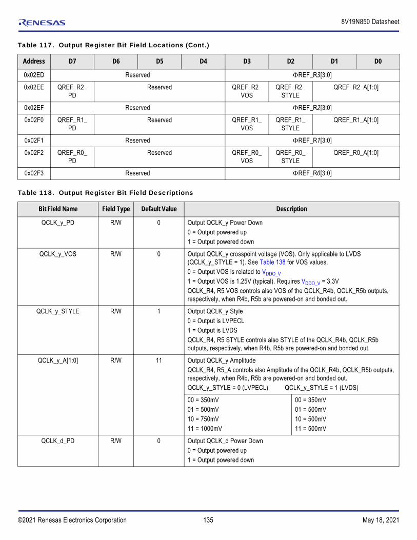
135©2021 Renesas Electronics Corporation May 18, 2021
8V19N850 Datasheet
0x02ED Reserved REF_R3[3:0]
0x02EE QREF_R2_PD
Reserved QREF_R2_VOS
QREF_R2_STYLE
QREF_R2_A[1:0]
0x02EF Reserved REF_R2[3:0]
0x02F0 QREF_R1_PD
Reserved QREF_R1_VOS
QREF_R1_STYLE
QREF_R1_A[1:0]
0x02F1 Reserved REF_R1[3:0]
0x02F2 QREF_R0_PD
Reserved QREF_R0_VOS
QREF_R0_STYLE
QREF_R0_A[1:0]
0x02F3 Reserved REF_R0[3:0]
Table 118. Output Register Bit Field Descriptions
Bit Field Name Field Type Default Value Description
QCLK_y_PD R/W 0 Output QCLK_y Power Down0 = Output powered up1 = Output powered down
QCLK_y_VOS R/W 0 Output QCLK_y crosspoint voltage (VOS). Only applicable to LVDS (QCLK_y_STYLE = 1). See Table 138 for VOS values.0 = Output VOS is related to VDDO_V
1 = Output VOS is 1.25V (typical). Requires VDDO_V = 3.3VQCLK_R4, R5 VOS controls also VOS of the QCLK_R4b, QCLK_R5b outputs, respectively, when R4b, R5b are powered-on and bonded out.
QCLK_y_STYLE R/W 1 Output QCLK_y Style0 = Output is LVPECL1 = Output is LVDSQCLK_R4, R5 STYLE controls also STYLE of the QCLK_R4b, QCLK_R5b outputs, respectively, when R4b, R5b are powered-on and bonded out.
QCLK_y_A[1:0] R/W 11 Output QCLK_y AmplitudeQCLK_R4, R5_A controls also Amplitude of the QCLK_R4b, QCLK_R5b outputs, respectively, when R4b, R5b are powered-on and bonded out.QCLK_y_STYLE = 0 (LVPECL) QCLK_y_STYLE = 1 (LVDS)
00 = 350mV01 = 500mV10 = 750mV11 = 1000mV
00 = 350mV01 = 500mV10 = 500mV11 = 500mV
QCLK_d_PD R/W 0 Output QCLK_d Power Down0 = Output powered up1 = Output powered down
Table 117. Output Register Bit Field Locations (Cont.)
Address D7 D6 D5 D4 D3 D2 D1 D0
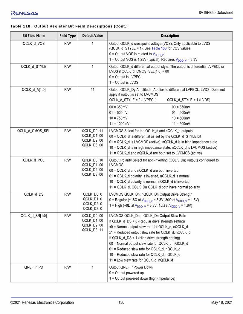
136©2021 Renesas Electronics Corporation May 18, 2021
8V19N850 Datasheet
QCLK_d_VOS R/W 1 Output QCLK_d crosspoint voltage (VOS). Only applicable to LVDS (QCLK_d_STYLE = 1). See Table 138 for VOS values.0 = Output VOS is related to VDDO_V
1 = Output VOS is 1.25V (typical). Requires VDDO_V = 3.3V
QCLK_d_STYLE R/W 1 Output QCLK_d differential output style. The output is differential LVPECL or LVDS if QCLK_d_CMOS_SEL[1:0] = 000 = Output is LVPECL1 = Output is LVDS
QCLK_d_A[1:0] R/W 11 Output QCLK_Dy Amplitude. Applies to differential LVPECL, LVDS. Does not apply if output is set to LVCMOSQCLK_d_STYLE = 0 (LVPECL) QCLK_d_STYLE = 1 (LVDS)
00 = 350mV01 = 500mV10 = 750mV11 = 1000mV
00 = 350mV01 = 500mV10 = 500mV11 = 500mV
QCLK_d_CMOS_SEL R/W QCLK_D0: 11QCLK_D1: 00QCLK_D2: 00QCLK_D3: 00
LVCMOS Select for the QCLK_d and nQCLK_d outputs00 = QCLK_d is differential as set by the QCLK_d_STYLE bit01 = QCLK_d is LVCMOS (active), nQCLK_d is in high impedance state10 = QCLK_d is in high impedance state, nQCLK_d is LVCMOS (active)11 = QCLK_d and nQCLK_d are both set to LVCMOS (active)
QCLK_d_POL R/W QCLK_D0: 10QCLK_D1: 00QCLK_D2: 00QCLK_D3: 00
Output Polarity Select for non-inverting (QCLK_Dn) outputs configured to LVCMOS00 = QCLK_d and nQCLK_d are both inverted01 = QCLK_d polarity is inverted, nQCLK_d is normal10 = QCLK_d polarity is normal, nQCLK_d is inverted11 = QCLK_d, QCLK_Dn QCLK_d both have normal polarity
QCLK_d_DS R/W QCLK_D0: 0QCLK_D1: 0QCLK_D2: 0QCLK_D3: 0
LVCMOS QCLK_Dn, nQCLK_Dn Output Drive Strength0 = Regular (~18Ω at VDDO_V = 3.3V, 30Ω at VDDO_V = 1.8V)1 = High (~9Ω at VDDO_V = 3.3V, 15Ω at VDDO_V = 1.8V)
QCLK_d_SR[1:0] R/W QCLK_D0: 00QCLK_D1: 00QCLK_D2: 00QCLK_D3: 11
LVCMOS QCLK_Dn, nQCLK_Dn Output Slew RateIf QCLK_d_DS = 0 (Regular drive strength setting)x0 = Normal output slew rate for QCLK_d, nQCLK_dx1 = Reduced output slew rate for QCLK_d, nQCLK_dIf QCLK_d_DS = 1 (High drive strength setting)00 = Normal output slew rate for QCLK_d, nQCLK_d01 = Reduced slew rate for QCLK_d, nQCLK_d10 = Reduced slew rate for QCLK_d, nQCLK_d11 = Low slew rate for QCLK_d, nQCLK_d
QREF_r_PD R/W 1 Output QREF_r Power Down0 = Output powered up1 = Output powered down (high-impedance)
Table 118. Output Register Bit Field Descriptions (Cont.)
Bit Field Name Field Type Default Value Description

137©2021 Renesas Electronics Corporation May 18, 2021
8V19N850 Datasheet
QREF_r_VOS R/W 1 Output QREF_r crosspoint voltage (VOS). Only applicable to LVDS (QREF_r_STYLE = 1). See Table 138 for VOS values.0 = Output VOS is related to VDDO_V
1 = Output VOS is 1.25V (typical). Requires VDDO_V = 3.3V
QREF_r_STYLE R/W 1 Output QREF_r Style0 = Output is LVPECL1 = Output is LVDS
QREF_r_A[1:0] R/W 10 Output QREF_r Amplitude.QREF_r_STYLE = 0 (LVPECL) QREF_r_STYLE = 1 (LVDS)
00 = 350mV01 = 500mV10 = 750mV11 = 1000mV
00 = 350mV01 = 500mV10 = 500mV11 = 500mV
ΦREF_Rr[3:0] R/W 1000 SYSREF Output Rr Fine Phase DelayThe delay is composed of 7 digital delay steps (half-period of the RF-PLL, 169ps) coded in bits [3:1] and an analog delay step coded in bit [0]. The analog delay step may vary from 60ps and 90ps over PVT.Delay in ps = ΦREF_Rr[3:1] 169ps + ΦREF_Rr[0] 75ps0000 = 0ps0001 = 75ps0010 = 169ps0011 = 169ps + 75ps = 244ps0100 = 339ps0101 = 339ps + 75ps = 414ps…1110 = 1186ps1111 = 1186ps + 75ps = 1,261ps
Table 118. Output Register Bit Field Descriptions (Cont.)
Bit Field Name Field Type Default Value Description

138©2021 Renesas Electronics Corporation May 18, 2021
8V19N850 Datasheet
GPIO RegistersTable 119. GPIO Register Bit Field Locations
Address D7 D6 D5 D4 D3 D2 D1 D0
0x0300 Reserved GPIO_0_TYPE GPIO_0_FUNC[3:0]
0x0301 Reserved GPIO_1_TYPE GPIO_1_FUNC[3:0]
0x0302 Reserved GPIO_2_TYPE GPIO_2_FUNC[3:0]
0x0303 Reserved GPIO_3_TYPE GPIO_3_FUNC[3:0]
Table 120. GPIO Register Bit Field Descriptions
Bit Field Name Field Type Default Value Description
GPIO_n_TYPEn = 0 to 3
R/W GPIO_0: 0GPIO_1: 0GPIO_2: 1GPIO_3: 1
Type of the GPIO pin0 = GPIO pin is input1 = GPIO pin is outputGPIO_0: pin 19GPIO_1: pin 20GPIO_2: pin 21GPIO_3: pin 22GPIO_n_TYPE can be changed at any time after the device completed its startup, indicated by READY at the GPIO_3 pin and the register bit DEVICE_RDY_STS.GPIO_n_TYPE is not copied into the device in an EEPROM load operation.
GPIO_0_FUNC R/W 0110 Function of the GPIO_0 pin. See also Table 26 for details and the definition of the output groups 0-6.0000 = Interrupt0001 = Input0 valid status0010 = Debug: DPLL-1 feedback clock0011 = DPLL-1 lock status0100 = APLL-0 lock status0101 = APLL-1 lock status0110 = DPLL-0 input selection0111 = CLK_0 disqualify1000 = CLK_1 disqualify1001 = Output group 0 enable1010 = Output group 1 enable1011 = Output group 2 enable1100 = Output group 3 enable1101 = Output group 4 enable1110 = Output group 5 enable1111 = Output group 6 enableGPIO_0_FUNC can be changed at any time after the device completed its startup, indicated by READY at the GPIO_3 pin and the register bit DEVICE_RDY_STS.GPIO_0_FUNC is not copied into the device in an EEPROM load operation.
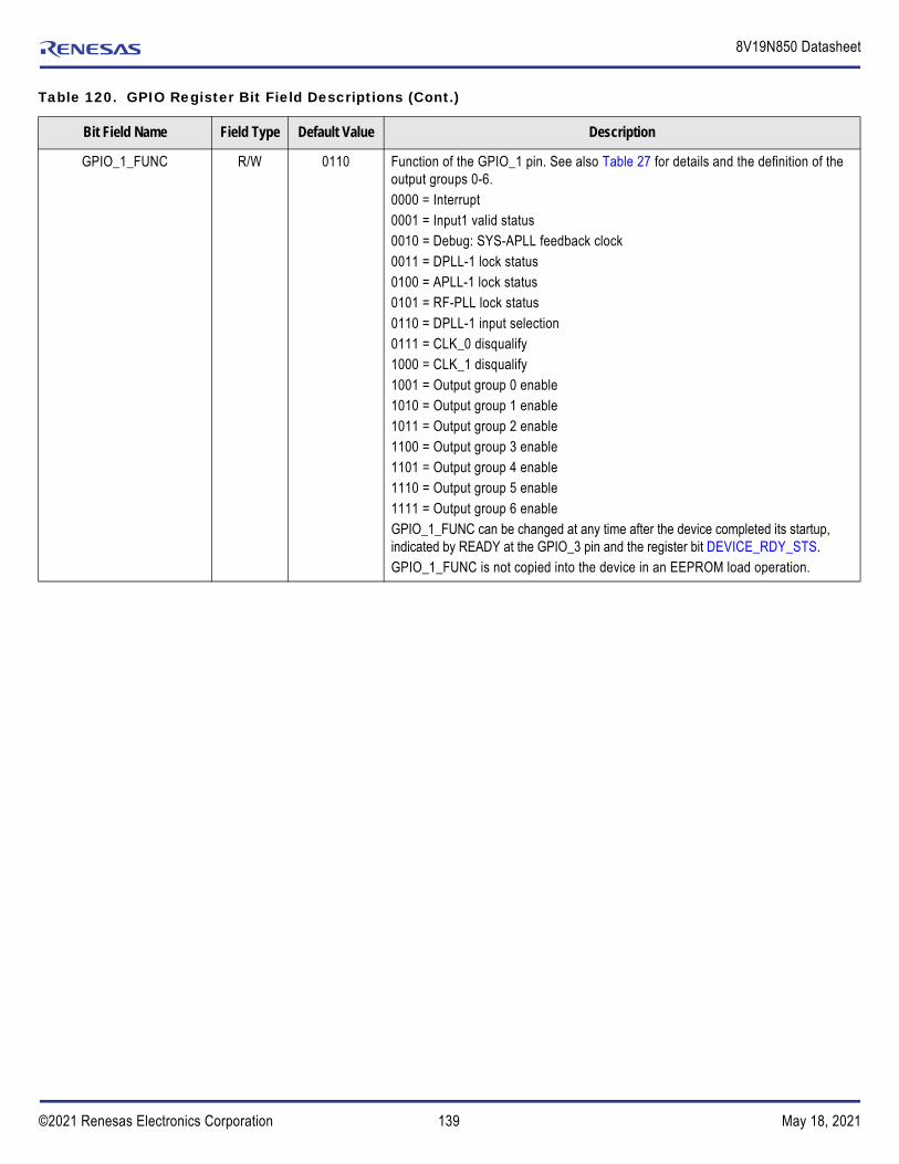
139©2021 Renesas Electronics Corporation May 18, 2021
8V19N850 Datasheet
GPIO_1_FUNC R/W 0110 Function of the GPIO_1 pin. See also Table 27 for details and the definition of the output groups 0-6.0000 = Interrupt0001 = Input1 valid status0010 = Debug: SYS-APLL feedback clock0011 = DPLL-1 lock status0100 = APLL-1 lock status0101 = RF-PLL lock status0110 = DPLL-1 input selection0111 = CLK_0 disqualify1000 = CLK_1 disqualify1001 = Output group 0 enable1010 = Output group 1 enable1011 = Output group 2 enable1100 = Output group 3 enable1101 = Output group 4 enable1110 = Output group 5 enable1111 = Output group 6 enableGPIO_1_FUNC can be changed at any time after the device completed its startup, indicated by READY at the GPIO_3 pin and the register bit DEVICE_RDY_STS.GPIO_1_FUNC is not copied into the device in an EEPROM load operation.
Table 120. GPIO Register Bit Field Descriptions (Cont.)
Bit Field Name Field Type Default Value Description

140©2021 Renesas Electronics Corporation May 18, 2021
8V19N850 Datasheet
GPIO_2_FUNC R/W 1010 Function of the GPIO_2 pin. See also Table 28 for details and the definition of the output groups 0-6.0000 = Interrupt0001 = CLK_0 valid status0010 = DPLL-0 holdover status0011 = DPLL-1 holdover status0100 = DPLL-0 lock status0101 = DPLL-1 lock status0110 = APLL-0 lock status0111 = RF-PLL lock status1000 = DPLL-0 input selection1001 = Output group 0 enable1010 = Output group 1 enable1011 = Output group 2 enable1100 = Output group 3 enable1101 = Output group 4 enable1110 = Output group 5 enable1111 = Output group 6 enableGPIO_2_FUNC can be changed at any time after the device completed its startup, indicated by READY at the GPIO_3 pin and the register bit DEVICE_RDY_STS.GPIO_2_FUNC is not copied into the device in an EEPROM load operation.
GPIO_3_FUNC R/W 0011 Function of the GPIO_3 pin. See also Table 29 for details and the definition of the output groups 0-6.0000 = Interrupt0001 = CLK_0 valid status0010 = CLK_1 valid status0011 = Device ready status0100 = DPLL-0 lock status0101 = DPLL-1 lock status0110 = APLL-0 lock status0111 = APLL-2 lock status1000 = DPLL-1 input selection1001 = Output group 0 enable1010 = Output group 1 enable1011 = Output group 2 enable1100 = Output group 3 enable1101 = Output group 4 enable1110 = Output group 5 enable1111 = Output group 6 enableGPIO_3_FUNC can be changed at any time after the device completed its startup, indicated by READY at the GPIO_3 pin and the register bit DEVICE_RDY_STS.GPIO_3_FUNC is not copied into the device in an EEPROM load operation.
Table 120. GPIO Register Bit Field Descriptions (Cont.)
Bit Field Name Field Type Default Value Description

141©2021 Renesas Electronics Corporation May 18, 2021
8V19N850 Datasheet
Device Status
Address D7 D6 D5 D4 D3 D2 D1 D0
0x0317 ST_CAL_FIN_ALL
ST_I2C_MASTER_CLK_E
N
ST_INITREF Reserved Reserved Reserved Reserved ST_INITCLK
Bit Field Name Field Type Default Value Description
ST_CAL_FIN_ALL R/O 0 PLL calibration status0 = APLL calibration not completed1 = All APLLs have completed calibration (VCO band selection)
ST_I2C_MASTER_CLK_EN R/O 0 Master clock activation status0 = Not active.1 = Active.
ST_INIT_REF INIT_REF Synchronization Status. Indicates if QREF_r outputs are active and synchronized to QCLK_y outputs.0 = Not synchronized or no active SYSREF event1 = One or more QREF_r outputs are active and synchronized to the QCLK_y outputs.
ST_INITCLK R/O Internal initialization sequence status0 = INIT_CLK_ x initialization sequence is completed1 = INIT_CLK_ x initialization sequence active or stuckx = A, B, C, D

142©2021 Renesas Electronics Corporation May 18, 2021
8V19N850 Datasheet
DPLL-0/DPLL-1/APLL-2/RF-PLL StatusTable 121. DPLL-0/DPLL-1/APLL-2/RF-PLL Field Locations
Address D7 D6 D5 D4 D3 D2 D1 D0
0x0318 ST_DBIT_APLL0[7:0]
0x0319 Reserved ST_LOCK_APLL0
ST_CAL_OV_APLL0
ST_CAL_FIN_APLL0
ST_DBIT_APLL0[8]
0x031A ST_DBIT_APLL1[7:0]
0x031B Reserved ST_LOCK_APLL1
ST_CAL_OV_APLL1
ST_CAL_FIN_APLL1
ST_DBIT_APLL1[8]
0x031C ST_DBIT_APLL2[7:0]
0x031D Reserved ST_LOCK_APLL2
ST_CAL_OV_APLL2
ST_CAL_FIN_APLL2
ST_DBIT_APLL2[8]
0x031E ST_DBIT_RFPLL[7:0]
0x031F Reserved ST_LOCK_RFPLL
ST_CAL_OV_RFPLL
ST_CAL_FIN_RFPLL
ST_DBIT_RFPLL[8]
Table 122. DPLL-0/DPLL-1/APLL-2/RF-PLL Field Locations
Bit Field Name Field Type Default Value Description
ST_DBIT_p[8:0]
p = APLL0, APLL1, APLL2, RFPLL
R/O 0 Frequency band selected by PLL calibration (binary number)
ST_CAL_FIN_p
p = APLL0, APLL1, APLL2, RFPLL
R/O 0 PLL calibration finish status0 = PLL calibration is not finished1 = PLL calibration is finished
ST_CAL_OV_p
p = APLL0, APLL1, APLL2, RFPLL
R/O 0 PLL calibration overflow status0 = PLL calibration without overflow1 = PLL calibration with overflow
ST_LOCK_p
p = APLL0, APLL1, APLL2, RFPLL
R/O 0 PLL lock status0 = PLL is not locked1 = PLL is locked

143©2021 Renesas Electronics Corporation May 18, 2021
8V19N850 Datasheet
Initialization and Internal SYSREF TriggerTable 123. Initialization and Internal SYSREF Trigger Field Locations
Address D7 D6 D5 D4 D3 D2 D1 D0
0x0320 RELOCK Reserved
0x0321 INIT_CLK_A Reserved
0x0322 INIT_CLK_B Reserved
0x0323 INIT_CLK_C Reserved
0x0324 INIT_CLK_D Reserved
0x0325 INIT_REF Reserved
Table 124. Initialization and Internal SYSREF Trigger Field Descriptions
Bit Field Name Field Type Default Value Description
RELOCK W1AC 0 Re-start APLL calibration. Re-initializes calibration for all enabled APLLs.0 = No calibration restart1 = Re-lock the PLL calibration
INIT_CLK_A W1AC 0 Resets and synchronizes the following frequency dividers: DPLL-0 feedback divider M DPLL-0 the post divider (P0) Output dividers N_d that are driven by DPLL-0/APLL-0The divider reset is part of the a procedure to phase-align the DPLL-0 clock input to clock outputs driven by DPLL-0/APLL-0 (for information, see Input to Output Phase Alignment). During reset, the APLL-0 VCO clock is blocked from driving the dividers. Upon release from reset, the divider state machines are started at the same time and are synchronized to each other.0 = No reset1 = Reset/Synchronization
INIT_CLK_B W1AC 0 Resets and synchronizes the following frequency dividers: DPLL-1 feedback divider M DPLL-1 the post divider (P0)The divider reset is part of the a procedure to phase-align the DPLL-1 clock input to clock outputs driven by DPLL-1/APLL-1 (for information, see Input to Output Phase Alignment). During reset, the APLL-1 VCO clock is blocked from driving the dividers. Upon release from reset, the divider state machines are started at the same time and are synchronized to each other.0 = No reset1 = Reset/Synchronization

144©2021 Renesas Electronics Corporation May 18, 2021
8V19N850 Datasheet
INIT_CLK_C W1AC 0 Resets and synchronizes the following frequency dividers: APLL-2 feedback divider M Output dividers N_d that are driven by APLL-2The divider reset is part of the a procedure to phase-align the selected clock input to clock outputs driven by APLL-2 (for information, see Input to Output Phase Alignment). During reset, the APLL-2 VCO clock is blocked from driving the dividers. Upon release from reset, the divider state machines are started at the same time and are synchronized to each other.0 = No reset1 = Reset/Synchronization
INIT_CLK_D W1AC 0 Resets and synchronizes the following frequency dividers: RF-PLL feedback divider M Output dividers N_x, N_r, N_D2, N_D3 that are driven by RF-PLLThe divider reset is part of the a procedure to phase-align the selected clock input to clock outputs driven by the RF-PLL (for information, see Input to Output Phase Alignment). During reset, the RF_PLL VCO clock is blocked from driving the dividers. Upon release from reset, the divider state machines are started at the same time and are synchronized to each other.0 = No reset1 = Reset/Synchronization
INIT_REF W1AC 0 1 = Starts an initialization (synchronization) for the SYSREF divider N_S
Table 124. Initialization and Internal SYSREF Trigger Field Descriptions (Cont.)
Bit Field Name Field Type Default Value Description

145©2021 Renesas Electronics Corporation May 18, 2021
8V19N850 Datasheet
Channel Enable and PLL Reference Registers DescriptionsTable 125. Channel Enable and PLL Reference Field Locations
Address D7 D6 D5 D4 D3 D2 D1 D0
0x0326 EN_D0 EN_D1 EN_D2 EN_D3 EN_R5 EN_R4 EN_R3R2 EN_R1R0
0x0327 RDIV_SYSAPLL
RSEL_APLL0/1
RSEL_SYSAPLL
Reserved QREF_ALL_EN
Table 126. Channel Enable Field Descriptions
Bit Field Name Field Type Default Value Description
EN_D0 R/W 1 Output Enable QCLK_d (d = 0 to 3)0 = Disabled1 = Enabled
EN_D1 R/W 1
EN_D2 R/W 1
EN_D3 R/W 1
EN_R5 R/W 1 Enable output QCLK_R5.0 = Disabled1 = Enabled
EN_R4 R/W 1 Enable output QCLK_R4.0 = Disabled1 = Enabled
EN_R3R2 R/W 1 Enable output QCLK_R2 and QCLK_R30 = Disabled1 = Enabled
EN_R1R0 R/W 1 Enable output QCLK_R1 and QCLK_R00 = Disabled1 = Enabled
RDIV_SYSAPLL R/W 0 Reference clock divider for SYS-APLL0 = fREF,SYSAPLL = f (selected reference) ÷ 21 = fREF,SYSAPLL = f (selected reference) ÷ 1Set to 1 if the selected reference frequency (OSCI/OSCO or XO_DLL input frequency, selected by RSEL_APLL0/1) is less than 27MHz, otherwise select ÷2.
RSEL_APLL0/1 R/W 1
Value: Select XO_DPLL
input
Selects between crystal oscillator (OSCI/OSCO) and external oscillator (XO_DPLL) reference frequency source for APLL-0 and APLL-1.0 = Select OSC (crystal oscillator) input as source1 = Select XO_DPLL input as source

146©2021 Renesas Electronics Corporation May 18, 2021
8V19N850 Datasheet
RSEL_SYSAPLL R/W 0
Value: XO_DPLL
input
Selects between crystal oscillator (OSC) and external oscillator (XO_DPLL) reference frequency source for the SYS-APLL.0 = Select XO_DPLL input as source1 = Select OSCI/OSCO (crystal oscillator) inputs as source
QREF_ALL_EN R/W 0 Disables/Enables the QREF function. When enabled: Outputs are in low/high state if SYSREF_AC=0 and biased to midpoint if SYSREF_AC=10 = QREF function is disabled1 = QREF function is enabled
Table 127. EEPROM Registers
Address D7 D6 D5 D4 D3 D2 D1 D0
0x0337 EEPROM_VERSION
0x0339 CHECKSUM[7:0]
Table 126. Channel Enable Field Descriptions (Cont.)
Bit Field Name Field Type Default Value Description

147©2021 Renesas Electronics Corporation May 18, 2021
8V19N850 Datasheet
Electrical Characteristics
Absolute Maximum RatingsThe absolute maximum ratings are stress ratings only. Stresses greater than those listed below can cause permanent damage to the device. Functional operation of the 8V19N850 at absolute maximum ratings is not implied. Exposure to absolute maximum rating conditions may affect device reliability.
Table 128. EEPROM Registers Bit Field Descriptions
Bit Field Name Field Type Default Value Description
EEPROM_VERSION R – EEPROM version. The content of this register is copied from the EEPROM at the same offset address and acts as a EEPROM version register. Content of this register is also included in the checksum in register 0x0339. Values can only be read through the SPI and I3C/I2C interface, but not written.
CHECKSUM R – EEPROM checksum including content of register 0x0337.
Table 129. Absolute Maximum Ratings
Item Rating
Supply Voltage, VDD_V, VDDO_V 3.6V
Inputs -0.5V to VDD_V + 0.5V
Outputs, VO (LVCMOS) -0.5V to VDDO_V + 0.5V
Outputs, IO (LVPECL) Continuous Current Surge Current
50mA100mA
Outputs, IO (LVDS)Continuous CurrentSurge Current
50mA100mA
Input termination current, IVT ±35mA
Junction Temperature, TJ 150C
Storage Temperature, TSTG -65C to 150C
ESD - Human Body Modela
a. According to JEDEC JS-001-2012/JESD22-C101
2000V
ESD - Charged Device Modela 500V
Table 130. Recommended Operating Conditions
Item Rating
Supply Voltage, VDD_V 3.3V
Supply Voltage, VDDO_V 3.3V, 2.5V, 1.8V
Operating Junction Temperature, TJa
a. 125C/10year lifetime is based on the evaluation of intrinsic wafer process technology reliability metrics. The limiting wafer level reliability factor for this technology with respect to high temperature operation is electromigration. The device is verified to the maximum operating junction temperature through simulation.
≤ 125C
Board Temperature, TB ≤ 105C

148©2021 Renesas Electronics Corporation May 18, 2021
8V19N850 Datasheet
Pin Characteristics
External Oscillator Characteristics
Table 131. Pin Characteristics, VDD_V = 3.3V ±5%, TA = -40°C to +105°C (Case)
Symbol Parameter Test Conditions Minimum Typical Maximum Units
CINa
a. Guaranteed by design
Input Capacitance 2 4 pF
Other inputs 2 4 pF
RPU Input Pull-Up Resistor 51 k
RPU Input Pull-Down Resistor 51 k
ROUT LVCMOS Output Impedance 25
Table 132. External Crystal/Oscillator Characteristics, VDD_V = 3.3V ±5%, VDDO_V = (3.3V, 2.5V, 1.8V) ±5%, TA = -40°C to +105°C (Case) a
a. Electrical parameters are guaranteed over the specified ambient operating temperature range, which is established when the device is mounted in a test socket with maintained transverse airflow greater than 500 lfpm. The device will meet specifications after thermal equilibrium has been reached under these conditions.
Symbol Parameter Test Conditions Minimum Typical Maximum Units
Crystal (OSCI, OSCO)
Mode of Oscillation Fundamental
fXTAL Crystal Frequency 25 54 MHz
ESR Equivalent Series Resistance CL= 12pF 30
CL Load capacitance 12 pF
OSCI Overdriven by External Signalb (OSCO is left open)
b. XO, TCXO, or OCXO. In this mode, the XO_DPLL is not used and the SYS-DPLL can be turned off.
fXO XO Frequency To APLL-0, APLL-1 or APLL-2 25 100 MHz
To SYS-APLL 10 54 MHz
XO_DPLLc
c. TCXO or OCXO when used for SYS-DPLL only; otherwise, see fXO for limits.
fTCXO XO Frequency To SYS-DPLL 10 72d
d. Based on (SYS_CLK/3)*2, where SYS_CLK is approximately 108MHz.
MHz

149©2021 Renesas Electronics Corporation May 18, 2021
8V19N850 Datasheet
DC CharacteristicsTable 133. Power Supply DC Characteristics, TA = -40°C to +105°C (Case) a
a. Electrical parameters are guaranteed over the specified ambient operating temperature range, which is established when the device is mounted in a test socket with maintained transverse airflow greater than 500 lfpm. The device will meet specifications after thermal equilibrium has been reached under these conditions.
Symbol Parameter Test Conditions Minimum Typical Maximum Units
VDD_V Core Supply Voltage JESD8C-01 Narrow Range 3.135 3.3 3.465 V
VDDO_V Output Supply Voltage JESD8C-01 Narrow Range 3.135 3.3 3.465 V
2.375 2.5 2.625 V
1.71 1.8 1.89 V
IDD_TOT Total Power Supply Currentb
b. Applicable to the default startup configuration 00
VDD_V=3.3V, VDDO_V = 2.5V(except VDDO_D0 = 3.3V)
1.34 1.472 A
IDD_TOT Total Power Supply Currentc
c. Applicable to the default startup configuration 01
VDD_V=3.3V, VDDO_V = 2.5V 1.39 1.528 A
IDD_TOT Total Power Supply Currentd
d. Applicable to the default startup configuration 10
VDD_V=3.3V, VDDO_V = 2.5V(except VDDO_D2 = VDDO_D3 = 3.3V)
1.57 1.725 A
IDD_TOT Total Power Supply Currente
e. Applicable to the default startup configuration 11
VDD_V=3.3V, VDDO_V = 3.3V 1.48 1.626 A
Table 134. LVCMOS Input DC Characteristics, VDD_V = 3.3V ±5%, VDDO_V = (3.3V, 2.5V, 1.8V) ±5%, TA = -40°C to +105°C (Case) a
Symbol Parameter Test Conditions Minimum Typical Maximum Units
Control Input SPI_SEL (LVCMOS Logic)
VIH Input High Voltage
0.65 × VDDO_R5
0.5 × VDDO_R5
VDDO_R5 V
VIL Input Low Voltage
-0.3 0.35 × VDDO_R5
V
IIH InputHigh Current
Input with pull-up resistor VDD_V = 3.3V, VIN = 3.3V 10 µA
IIL InputLow Current
VDD_V = 3.3V, VIN = 0V -150 µA
SYSREF Trigger Input EXT_SYS (LVCMOS Logic)
VIH Input High Voltage
1.8V logic 1.17 VDD_V V
VIL Input Low Voltage
1.8V logic -0.3 0.63 V

150©2021 Renesas Electronics Corporation May 18, 2021
8V19N850 Datasheet
IIH InputHigh Current
Input with pull-down resistor
VDD_V = 3.3V, VIN = 1.8V or 3.3V 150 µA
IIL InputLow Current
VDD_V = 3.3V, VIN = 0V -10 µA
SPI Inputs: SDI, SCLK, nCS (1.8V Logic with Input Hysteresis)
VI Input Voltage -0.3 VDD_V V
VT+ Positive-going input threshold
voltage
0.660 1.350 V
VT- Negative-going input threshold
voltage
0.495 1.170 V
VH Hysteresis Voltage
VT+ - VT- 0.165 0.780 V
a. Electrical parameters are guaranteed over the specified ambient operating temperature range, which is established when the device is mounted in a test socket with maintained transverse airflow greater than 500 lfpm. The device will meet specifications after thermal equilibrium has been reached under these conditions.
Table 135. LVCMOS Output DC Characteristics, VDD_V = 3.3V ±5%, VDDO_V = (3.3V, 2.5V, 1.8V) ±5%, TA = -40°C to +105°C (Case) a
Symbol Parameter Test Conditions Minimum Typical Maximum Units
QCLK_Dn (LVCMOS)
VOHOutput
High Voltage
Per JESD8C-01 VDDO_V = 3.3V, IOH = -8mA 2.4 V
Per JESD5-5A-01 VDDO_V = 2.5V, IOH = -4mA 1.7 V
Per JESD8-7A VDDO_V = 1.8V, IOH = -4mA VDDO_V - 0.45 V
VOLOutput
Low Voltage
Per JESD8C-01 VDDO_V = 3.3V, IOH = -8mA 0.40 V
Per JESD5-5A-01 VDDO_V = 2.5V, IOH = -4mA 0.70 V
Per JESD8-7A VDDO_V = 1.8V, IOH = -4mA 0.45 V
ZOUTOutput
Impedance
QCLK_d_DS = 0QCLK_d_DS = 1
VDDO_V = 3.3V 158
ΩΩ
QCLK_d_DS = 0QCLK_d_DS = 1
VDDO_V = 2.5V 169
ΩΩ
QCLK_d_DS = 0QCLK_d_DS = 1
VDDO_V = 1.8V 2011
ΩΩ
Table 134. LVCMOS Input DC Characteristics, VDD_V = 3.3V ±5%, VDDO_V = (3.3V, 2.5V, 1.8V) ±5%, TA = -40°C to +105°C (Case) a
Symbol Parameter Test Conditions Minimum Typical Maximum Units
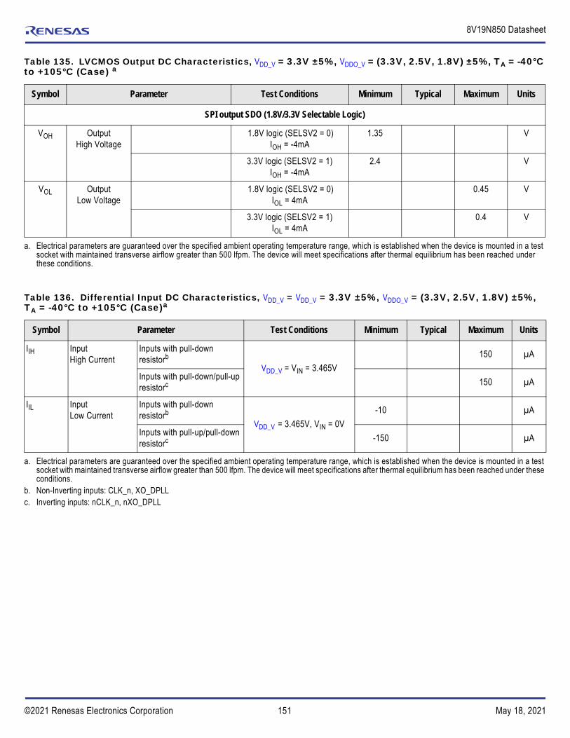
151©2021 Renesas Electronics Corporation May 18, 2021
8V19N850 Datasheet
SPI output SDO (1.8V/3.3V Selectable Logic)
VOH OutputHigh Voltage
1.8V logic (SELSV2 = 0)IOH = -4mA
1.35 V
3.3V logic (SELSV2 = 1)IOH = -4mA
2.4 V
VOL OutputLow Voltage
1.8V logic (SELSV2 = 0)IOL = 4mA
0.45 V
3.3V logic (SELSV2 = 1)IOL = 4mA
0.4 V
a. Electrical parameters are guaranteed over the specified ambient operating temperature range, which is established when the device is mounted in a test socket with maintained transverse airflow greater than 500 lfpm. The device will meet specifications after thermal equilibrium has been reached under these conditions.
Table 136. Differential Input DC Characteristics, VDD_V = VDD_V = 3.3V ±5%, VDDO_V = (3.3V, 2.5V, 1.8V) ±5%, TA = -40°C to +105°C (Case)a
a. Electrical parameters are guaranteed over the specified ambient operating temperature range, which is established when the device is mounted in a test socket with maintained transverse airflow greater than 500 lfpm. The device will meet specifications after thermal equilibrium has been reached under these conditions.
Symbol Parameter Test Conditions Minimum Typical Maximum Units
IIH InputHigh Current
Inputs with pull-down resistorb
b. Non-Inverting inputs: CLK_n, XO_DPLL
VDD_V = VIN = 3.465V
150 µA
Inputs with pull-down/pull-up resistorc
c. Inverting inputs: nCLK_n, nXO_DPLL
150 µA
IIL InputLow Current
Inputs with pull-down resistorb
VDD_V = 3.465V, VIN = 0V
-10 µA
Inputs with pull-up/pull-down resistorc -150 µA
Table 135. LVCMOS Output DC Characteristics, VDD_V = 3.3V ±5%, VDDO_V = (3.3V, 2.5V, 1.8V) ±5%, TA = -40°C to +105°C (Case) a
Symbol Parameter Test Conditions Minimum Typical Maximum Units

152©2021 Renesas Electronics Corporation May 18, 2021
8V19N850 Datasheet
Table 137. LVPECL DC Characteristics (QCLK_y, QREF_r, STYLE = 0), VDD_V = 3.3V ±5%, VDDO_V = (3.3V, 2.5V, 1.8V) ±5%, TA = -40°C to +105°C (Case)a
Symbol Parameter Test Conditions Minimum Typical Maximum Units
VOH Output High Voltageb 350mV Amplitude Setting VDDO_V - 0.98 V
500mV Amplitude Setting VDDO_V - 1.04 V
750mV Amplitude Settingc VDDO_V - 1.06 V
1000mV Amplitude Settingd VDDO_V - 1.12 V
VOL Output Low Voltageb 350mV Amplitude Setting VDDO_V - 1.32 V
500mV Amplitude Setting VDDO_V - 1.56 V
750mV Amplitude Settinge VDDO_V - 1.81 V
1000mV Amplitude Settingf VDDO_V - 2.09 V
a. Electrical parameters are guaranteed over the specified ambient operating temperature range, which is established when the device is mounted in a test socket with maintained transverse airflow greater than 500 lfpm. The device will meet specifications after thermal equilibrium has been reached under these conditions.
b. LVPECL outputs terminated with 50 to VDDO_V – 1.5V (350mV amplitude setting), VDDO_V – 1.75V (500mV amplitude setting), VDDO_V – 2.0V (750mV amplitude setting), VDDO_V – 2.25V (1000mV amplitude setting)
c. 750mV amplitude setting is available at VDDO_V = 3.3Vd. 1000mV amplitude setting is available at VDDO_V = 3.3Ve. 750mV amplitude setting is available at VDDO_V = 3.3Vf. 1000mV amplitude setting is available at VDDO_V = 3.3V
Table 138. LVDS DC Characteristics (QCLK_d, QCLK_y, QREF_r, STYLE = 1), VDD_V = 3.3V ±5%, VDDO_V = (3.3V, 2.5V, 1.8V) ±5%, TA = -40°C to +105°C (Case)a
a. Electrical parameters are guaranteed over the specified ambient operating temperature range, which is established when the device is mounted in a test socket with maintained transverse airflow greater than 500 lfpm. The device will meet specifications after thermal equilibrium has been reached under these conditions.
Symbol Parameter Test Conditions Minimum Typical Maximum Units
VOS Offset Voltageb
QCLK_d_VOS = 0QCLK_y_VOS = 0QREF_r_VOS = 0
b. VOS changes with VDDO_V
VDDO_V= 3.3V350mV Amplitude Setting 1.92 2.2 2.55 V
500mV Amplitude Setting 1.77 2.1 2.45 V
VDDO_V= 2.5V350mV Amplitude Setting 1.17 1.4 1.70 V
500mV Amplitude Setting 1.01 1.3 1.60 V
VDDO_V= 1.8V350mV Amplitude Setting 0.47 0.7 0.95 V
500mV Amplitude Setting 0.34 0.6 0.85 V
Offset Voltagec
c. VOS is internally regulated to 1.25V.
VDDO_V= 3.3V Any Amplitude Setting 1.13 1.25 1.54 V
VOS VOS Magnitude Change
10 70 mV

153©2021 Renesas Electronics Corporation May 18, 2021
8V19N850 Datasheet
AC Characteristics Table 139. AC Characteristics, VDD_V = 3.3V ±5%, VDDO_V = (3.3V, 2.5V, 1.8V) ±5%, TA = -40°C to +105°C (Case)a
Symbol Parameter Test Conditions Minimum Typical Maximum Units
RF-PLL and Device Clock Domain (VCO = 2949.12MHz)
fVCO VCO Frequency 2949.12 MHz
fOUT Output Frequency RF-PLL Clock Outputs QCLK_y
QCLK_y, N = ÷1 2949.12 MHz
QCLK_y, N = ÷6 491.52 MHz
… …
QCLK_y, any N 2949.12 ÷ N MHz
… …
QCLK_y, N = ÷3072 0.96 MHz
RF-PLL SYSREF Outputs QCLK_r
QREF_r, N = ÷96 30.72 MHz
QREF_r, N = ÷384 7.68 MHz
QREF_r, N = ÷1536 1.92 MHz
… …
QREF_r, N = ÷3072 0.96 MHz
APLL-2, Digital Clock Domain, (VCO = 3600-3868MHz)
fVCO VCO Frequency 3600 3868 MHz
DPLL-0/APLL-0 and DPLL-1/APLL-1
fCLK Input Frequency CLK_n 0.001(1PPSb)
1000 MHz
fVCO VCO frequency APLL-0 2450 2500 2580MHz
APLL-1 3932.16
VIN Input Voltage Amplitudec
CLK_n0.16 1.2 V
VDIFF_IN Differential Input
Voltage Amplitudec, dCLK_n
0.32 2.4 V
VCMR Common Mode Input Voltage0.92
VDD_V – (VIN / 2)
V

154©2021 Renesas Electronics Corporation May 18, 2021
8V19N850 Datasheet
Startup time Configuration 00 & 10 100 ms
Configuration 10
DPLL-0 Locked, CLK_0=156.25MHz9.2PPM offset between local XO and input(<40ns MTIE per G.8262)
15e s
Configuration 11
DPLL-0 & DPLL-1 Locked, CLK_1=15.36MHz9.2PPM offset between local XO and input(<65ns MTIE per 3GPP TS 36.133)
15f s
Output Characteristics
odc Output Duty Cycle QCLK_y, QREF_r Any frequency 45 50 55 %
| tPH-tPL g | at 122.88, 245.76, 491.52MHz
0 150 ps
QCLK_d Any frequency 45 50 55 %
| tPH-tPL | at 100, 125, 156.25, 312.5MHz
150 ps
tR / tF Output Rise/Fall Time QCLK_y, QCLK_r LVDS, 20% to 80% 45 250 ps
QCLK_dh LVDS, 20% to 80% 45 250 ps
QCLK_d (Normal slew rate, high drive strength setting)
LVCMOS, 20% to 80%210 315 ps
GPIO Outputs LVCMOS, 20%-80% 0.59 1 ns
SR Differential Output Slew Rate
QCLK_y, QCLK_r LVPECL, VDDO_V = 3.3VLVDS, VDDO_V = 3.3V
1.3 V/ns
QCLK_d LVPECL, VDDO_V = 3.3VLVDS, VDDO_V = 3.3V
1.9 V/ns
SR LVCMOS Output Slew Rate
QCLK_d, Normal slew rate
LVCMOS, VDDO_V = 3.3VQCLK_d_SR[1:0] = 00
3.7 V/ns
VO(PP)i QCLK_y, QREF_r,
LVPECL Output Voltage Amplitude, Peak-to-peak, see also Table 137
350mV Amplitude 491.52MHz320 mV
500mV Amplitude 491.52MHz 475 mV
750mV Amplitude 491.52MHz 675 mV
1000mV Amplitude 491.52MHz 875 mV
Table 139. AC Characteristics, VDD_V = 3.3V ±5%, VDDO_V = (3.3V, 2.5V, 1.8V) ±5%, TA = -40°C to +105°C (Case)a
Symbol Parameter Test Conditions Minimum Typical Maximum Units

155©2021 Renesas Electronics Corporation May 18, 2021
8V19N850 Datasheet
VO(PP)j QCLK_d LVPECL
Output Voltage Amplitude, Peak-to-peak, see also Table 137
350mV Amplitude 312.5MHz320 mV
500mV Amplitude 312.5MHz 490 mV
750mV Amplitude 312.5MHz 675 mV
1000mV Amplitude 312.5MHz 880 mV
VODk QCLK_y, QREF_r,
LVDS Output Voltage Swing, Peak-to-peak, see also Table 138
350mV Amplitude 491.52MHz 240 400 mV
500mV Amplitude 491.52MHz375 600 mV
VODl QCLK_d, LVDS
Output Voltage Swing, Peak-to-peak, see also Table 138
350mV Amplitude 312.5MHz 235 400 mV
500mV Amplitude 312.5MHz365 600 mV
Output Phase Change for Hitless Reference Switchingm
Switching to an input reference with frequency 960kHz n
100 300 ps
Switching to an input reference with frequency < 960kHz o
1 2.5 ns
RF-PLL Delay and Clock Phase Characteristics
tPD Propagation delay variation CLK_n to any QCLK_y, QCLK_r
-500 +500 ps
CLK_n to any QCLK_d -500 +500 ps
tsk(o) Output to output skew, outputs configured (static phase delay) for an incident edge
QCLK_y, QCLK_r to any QCLK_y, QCLK_r
74 ps
QCLK_d (LVDS) 50 ps
QCLK_y to any QCLK_d 60 ps
tPD SYSREF Propagation delay EXT_SYS to SYSREF output(SRG=000)p 0.8 2.2 ns
tS SYSREF Setup Time EXT_SYS to CLK_n(SRG = 001, configuration 01)q
-1
nstH SYSREF Hold Time 6
tW SYSREF Pulse Width SRG = 010 or 100 4
SRG = 001 (4Nx/Fvco)
tsk(o) Output to output skew variation (drift) over temperature
QCLK_y, QCLK_r to any QCLK_y, QCLK_r
1ps/°C
ΔΦ Output isolation between any neighboring clock output
QCLK_DnfOUT = 312.5MHz
65 58.5 dB
QCLK_ Rn,fOUT = 491.52MHz
76 74.8 dB
Table 139. AC Characteristics, VDD_V = 3.3V ±5%, VDDO_V = (3.3V, 2.5V, 1.8V) ±5%, TA = -40°C to +105°C (Case)a
Symbol Parameter Test Conditions Minimum Typical Maximum Units

156©2021 Renesas Electronics Corporation May 18, 2021
8V19N850 Datasheet
Figure 23. EXT_SYS Input Timing Diagram (SRG = 001)
ΔΦ Output isolation between any QCLK_y, QREF_r output
Both SYSREF and clock signals active
70.5 dB
PSNR Supply Noise Rejectionr 10kHz100kHz1MHz10MHz
10973
mV RMSmV RMSmV RMSmV RMS
PSNR Supply Noise Rejection
Sinusoidal signal injected.f =10Hz-1MHz
61.7 dB
Sinusoidal signal injected: f=1MHz-40MHz
84.5 dB
a. Electrical parameters are guaranteed over the specified ambient operating temperature range, which is established when the device is mounted in a test socket with maintained transverse airflow greater than 500 lfpm. The device will meet specifications after thermal equilibrium has been reached under these conditions.
b. Supports 1Hz / 1PPS utilizing a frequency snap and phase snap mechanism.c. VIL should not be less than -0.3V and VIH should not be greater than VDD_Vd. Common Mode Input Voltage is defined as the cross-point voltage.e. Based on default DPLL-0 settings for BW, damping, and lock threshold. Use of fast lock or tighter lock threshold will improve settling time.f. Based on default DPLL-0 and DPLL-1 settings for BW, damping, and lock threshold. Use of fast lock or tighter lock threshold will improve settling time.g. tPH = High pulse period; tPL = Low pulse period. h. Applicable to the default startup configurations 00 and 10. i. LVPECL outputs terminated with 50 to VDDO_V – 1.5V (350mV amplitude setting), VDDO_V – 1.75V (500mV amplitude setting), VDDO_V – 2.0V (750mV
amplitude setting), VDDO_V – 2.25V (1000mV amplitude setting and VDDO_V = 3.3V)j. LVPECL outputs terminated with 50 to VDDO_V – 1.5V (350mV amplitude setting), VDDO_V – 1.75V (500mV amplitude setting), VDDO_V – 2.0V (750mV
amplitude setting), VDDO_V – 2.25V (1000mV amplitude setting and VDDO_V = 3.3V)k. LVDS outputs terminated 100 across terminals. l. LVDS outputs terminated 100 across terminals. m. This parameter was measured with a low phase noise reference provided to the system APLL.n. Tested with 960kHz input reference, with modified Hitless Filter values (Avg = 7 and Shift = 16). o. Tested with 1kHz input reference, with modified Hitless Filter values (Avg = 7 and Shift = 14)p. Delay values in SYSREF path set to 0q. Configuration for SYSREF ext. trigger modes SRG=001: fIN = 30.72MHz and DPLL-1 locked using RF-PLL feedback, fIN-RFPLL = 122.88MHz, delay stages
set to 0, SYSREF = 7.68MHz. See Figure 23 for setup and hold time definition.r. PSNR is measured at a differential output pair with the criteria: output spurious specification is met with an injected sinusoidal signal at the specified
frequency and amplitude.
Table 139. AC Characteristics, VDD_V = 3.3V ±5%, VDDO_V = (3.3V, 2.5V, 1.8V) ±5%, TA = -40°C to +105°C (Case)a
Symbol Parameter Test Conditions Minimum Typical Maximum Units
CLK_n
EXT_SYS
QREF_r High Impedance
tS tH
Valid EXT_SYStW

157©2021 Renesas Electronics Corporation May 18, 2021
8V19N850 Datasheet
Table 140. RF-PLL Device Clock Domain QCLK_y Clock Phase Noise Characteristics, VDD_V = 3.3V ±5%, TA = -40°C to +105°C (Case) a b c d
Symbol Parameter Test Conditions Minimum Typical Maximum Units
tjit(Ø) RMS Phase Jitter (Random)RF-PLL Clock on QCLK_y, 491.52MHz
Integration Range: 1kHz – 100MHzDefault configuration 00Default configuration 01
168144
fs
Integration Range: 10kHz – 20MHzDefault configuration 00Default configuration 01
147123
250 fs
tjit(Ø) RMS Phase Jitter (Random)RF-PLL Clock on QCLK_y, 245.76MHz
Integration Range: 10kHz – 20MHzDefault configuration 10 129 250 fs
tjit(Ø) RMS Phase Jitter (Random)RF-PLL Clock on QCLK_y, 122.88MHz
Integration Range: 10kHz – 20MHzDefault configuration 00Default configuration 01Default configuration 10Default configuration 11
159136141162
250 fs
Ø(10) Clock Single-side Band Phase Noise
QCLK_y, 491.52MHze,f
10Hz offset -81.4 dBc/Hz
Ø(100) 100Hz offset -108 dBc/Hz
Ø(500) 500Hz offset from carrier -118.8 dBc/Hz
Ø(1k) 1kHz offset from carrier -120.9 -117.5 dBc/Hz
Ø(10k) 10kHz offset from carrier -125 -122.1 dBc/Hz
Ø(100k) 100kHz offset from carrier -128.8 -127.8 dBc/Hz
Ø(300k) 300kHz offset from carrier -132.4 -131.5 dBc/Hz
Ø(1M) 1MHz offset from carrier -140.6 -137.9 dBc/Hz
Ø(2M) 2MHz offset from carrier -152.7 -150.5 dBc/Hz
Ø(10M) 10MHz offset from carrier -157.7 -155.6 dBc/Hz
Ø(20M) 20MHz offset from carrier and noise floor
-158.3 -156 dBc/Hz
Ø(1) Clock Single-side Band Phase Noise
QCLK_y, 245.76MHzg
1Hz offset -56.6 dBc/Hz
Ø(10) 10Hz offset -85.5 dBc/Hz
Ø(100) 100Hz offset from carrier -113.3 dBc/Hz
Ø(1k) 1kHz offset from carrier -126 -120 dBc/Hz
Ø(10k) 10kHz offset from carrier -127 -123 dBc/Hz
Ø(100k) 100kHz offset from carrier -132.9 -131 dBc/Hz
Ø(300k) 300kHz offset from carrier -140.4 -137 dBc/Hz
Ø(1M) 1MHz offset from carrier -149.4 -144 dBc/Hz
Ø(2M) 2MHz offset from carrier -156.7 -153 dBc/Hz
ØN(10M) 10MHz offset from carrier -159.1 -157 dBc/Hz
ØN(20M) 20MHz offset from carrier and noise floor
-160.3 -155 dBc/Hz

158©2021 Renesas Electronics Corporation May 18, 2021
8V19N850 Datasheet
Ø(1) Clock Single-side Band Phase Noise
QCLK_y, 122.88MHzh
1Hz offset -65.1 dBc/Hz
Ø(10) 10Hz offset -91.3 dBc/Hz
Ø(100) 100Hz offset from carrier -117.8 dBc/Hz
Ø(1k) 1kHz offset from carrier -130.4 -126.2 dBc/Hz
Ø(10k) 10kHz offset from carrier -132.1 -129.3 dBc/Hz
Ø(100k) 100kHz offset from carrier -137.9 -135 dBc/Hz
Ø(300k) 300kHz offset from carrier -145.1 -141.2 dBc/Hz
Ø(1M) 1MHz offset from carrier -155.5 -148.2 dBc/Hz
Ø(2M) 2MHz offset from carrier -161.8 -158 dBc/Hz
ØN(10M) 10MHz offset from carrier -164.4 -162.5 dBc/Hz
ØN(20M) 20MHz offset from carrier and noise floor
-165 -163.3 dBc/Hz
Table 140. RF-PLL Device Clock Domain QCLK_y Clock Phase Noise Characteristics, VDD_V = 3.3V ±5%, TA = -40°C to +105°C (Case) a b c d (Cont.)
Symbol Parameter Test Conditions Minimum Typical Maximum Units

159©2021 Renesas Electronics Corporation May 18, 2021
8V19N850 Datasheet
Ø Spurious Signal Rejection(QCLK, QREF as clock)
491.52MHz 2Hz – <100HzDefault configuration 00Default configuration 01
58.655.7
dB
100Hz – <1kHzDefault configuration 00Default configuration 01
99.196.1
dB
1kHz – <983.04MHzDefault configuration 00Default configuration 01
68.277.1
dB
245.76MHz[g] 2Hz – <100Hz 62.5 dB
100Hz – <1kHz 103 dB
1kHz – <491.52MHz 83 dB
122.88MHz 2Hz – <100HzDefault configuration 00Default configuration 01Default configuration 10Default configuration 11
60.465.663.865.5
dB
100Hz – <1kHzDefault configuration 00Default configuration 01Default configuration 10Default configuration 11
‘104.9103.5104.787.5
dB
1kHz – <245.76MHzDefault configuration 00Default configuration 01Default configuration 10Default configuration 11
74.481.391.579.8
dB
Harmonic rejection
491.52MHz[e]
[f]Even order harmonics 47.5 dB
245.76MHz[g] 49.0 dB
122.88MHz[h] 50.3 dB
a. Phase noise and spurious specifications apply for device operation with QREF_r outputs active (SYSREF pulses generated).Phase noise specifications are applicable for all outputs active, N_x dividers not equal.
b. Electrical parameters are guaranteed over the specified ambient operating temperature range, which is established when the device is mounted in a test socket with maintained transverse airflow greater than 500lfpm. The device will meet specifications after thermal equilibrium has been reached under these conditions.
c. Phase noise characteristics at lower frequency offsets (1Hz ~1kHz) is primarily a function of the TCXO phase noise. TXCO: MX-503: -65dBc/Hz at 1Hz, -93dBc/Hz at 10Hz, -118dBc/Hz at 100Hz, -140dBc/Hz at 1kHz.
d. Test conditions and data are based on the default configurations. The phase noise performance can be improved by optimization of the configuration and/or re-arrangement of clock outputs. For more information, please contact Renesas.
e. Configuration 00f. Configuration 01g. Configuration 10h. Configuration 11
Table 140. RF-PLL Device Clock Domain QCLK_y Clock Phase Noise Characteristics, VDD_V = 3.3V ±5%, TA = -40°C to +105°C (Case) a b c d (Cont.)
Symbol Parameter Test Conditions Minimum Typical Maximum Units

160©2021 Renesas Electronics Corporation May 18, 2021
8V19N850 Datasheet
Table 141. Digital Clock Domain QCLK_d Clock Phase Noise Characteristics, VDD_V = 3.3V ±5%, TA = -40°C to +105°C (Case) a b c d
Symbol Parameter Test Conditions Minimum Typical Maximum Units
tjit(Ø) RMS Phase Jitter (Random)DPLL-0 (2500MHz) Clock on QCLK_d, 312.5MHHz
Integration Range: 10kHz – 20MHzDefault configuration 00Default configuration 01
292285
fs
tjit(Ø) RMS Phase Jitter (Random)DPLL-0 (2500MHz) Clock on QCLK_d, 156.25MHz
Integration Range: 10kHz – 20MHzDefault configuration 10Default configuration 11
257253
fs
Ø(100) Clock Single-side Band Phase Noise
QCLK_d, 100MHze,f
100Hz offset from carrier -121 dBc/Hz
Ø(1k) 1kHz offset from carrier -136.4 -133 dBc/Hz
Ø(10k) 10kHz offset from carrier -139.1 -132 dBc/Hz
Ø(100k) 100kHz offset from carrier -142.9 -141 dBc/Hz
Ø(1M) 1MHz offset from carrier -156.4 -154 dBc/Hz
Ø(10M) 10MHz offset from carrier and noise floor
-162.1 -160 dBc/Hz
Ø(100) Clock Single-side Band Phase Noise
QCLK_d, 156.25MHzg
100Hz offset -118.6 dBc/Hz
Ø(1k) 1kHz offset from carrier -131.8 -126 dBc/Hz
Ø(10k) 10kHz offset from carrier -134.5 -130 dBc/Hz
Ø(100k) 100kHz offset from carrier -137.6 -135 dBc/Hz
Ø(1M) 1MHz offset from carrier -150.8 -147 dBc/Hz
Ø(10M) 10MHz offset from carrier and noise floor
-155.3 -152 dBc/Hz
Ø(100) Clock Single-side Band Phase Noise
QCLK_d, 156.25MHzh
100Hz offset -113.9 dBc/Hz
Ø(1k) 1kHz offset from carrier -127.1 -120 dBc/Hz
Ø(10k) 10kHz offset from carrier -129.7 -123 dBc/Hz
Ø(100k) 100kHz offset from carrier -135.4 -131 dBc/Hz
Ø(1M) 1MHz offset from carrier -149 -143 dBc/Hz
Ø(10M) 10MHz offset from carrier and noise floor
-154.2 -152 dBc/Hz

161©2021 Renesas Electronics Corporation May 18, 2021
8V19N850 Datasheet
Ø(100) Clock Single-side Band Phase Noise
QCLK_d, 312.5MHz[e][f]
100Hz offset -112.3 dBc/Hz
Ø(1k) 1kHz offset from carrier -126.6 -122 dBc/Hz
Ø(10k) 10kHz offset from carrier -129.1 -125 dBc/Hz
Ø(100k) 100kHz offset from carrier -133 -131 dBc/Hz
Ø(1M) 1MHz offset from carrier -147.8 -144 dBc/Hz
Ø(10M) 10MHz offset from carrier and noise floor
-158.7 -155 dBc/Hz
Ø Spurious Signal Rejection(QCLK_d)
312.5MHz 100Hz – 625MHzDefault configuration 00Default configuration 01
63.660.6
dB
156.25MHz 100Hz – 312.5MHzDefault configuration 10Default configuration 11
64.456.6
dB
100MHz 100Hz – 200MHzDefault configuration 00Default configuration 01
66.766.7
dB
a. Phase noise and spurious specifications apply for device operation with QREF_r outputs active (SYSREF pulses generated).Phase noise specifications are applicable for all outputs active, N_x dividers not equal.
b. Electrical parameters are guaranteed over the specified ambient operating temperature range, which is established when the device is mounted in a test socket with maintained transverse airflow greater than 500lfpm. The device will meet specifications after thermal equilibrium has been reached under these conditions.
c. Phase noise characteristics at lower frequency offsets (1Hz ~1kHz) is primarily a function of the TCXO phase noise. TXCO: MX-503: -65dBc/Hz at 1Hz, -93dBc/Hz at 10Hz, -118dBc/Hz at 100Hz, -140dBc/Hz at 1kHz.
d. Test conditions and data are based on the default configurations. The phase noise performance can be improved by optimization of the configuration and/or re-arrangement of clock outputs. For more information, please contact Renesas.
e. Configuration 00f. Configuration 01g. Configuration 10h. Configuration 11
Table 141. Digital Clock Domain QCLK_d Clock Phase Noise Characteristics, VDD_V = 3.3V ±5%, TA = -40°C to +105°C (Case) a b c d (Cont.)
Symbol Parameter Test Conditions Minimum Typical Maximum Units
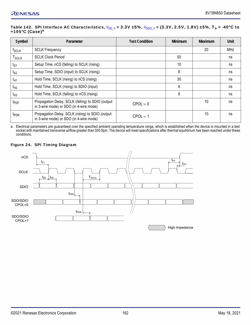
162©2021 Renesas Electronics Corporation May 18, 2021
8V19N850 Datasheet
Figure 24. SPI Timing Diagram
Table 142. SPI Interface AC Characteristics, VDD_V = 3.3V ±5%, VDDO_V = (3.3V, 2.5V, 1.8V) ±5%, TA = -40°C to +105°C (Case)a
Symbol Parameter Test Condition Minimum Maximum Unit
fSCLK SCLK Frequency 20 MHz
TSCLK SCLK Clock Period 50 ns
tS1 Setup Time, nCS (falling) to SCLK (rising) 10 ns
tS2 Setup Time, SDIO (input) to SCLK (rising) 8 ns
tH1 Hold Time, SCLK (rising) to nCS (rising) 30 ns
tH2 Hold Time, SCLK (rising) to SDIO (input) 8 ns
tH3 Hold Time, SCLK (falling) to nCS (rising) 8 ns
tPDF Propagation Delay, SCLK (falling) to SDIO (output in 3-wire mode) or SDO (in 4-wire mode)
CPOL 0 10 ns
tPDR Propagation Delay, SCLK (rising) to SDIO (output in 3-wire mode) or SDO (in 4-wire mode)
CPOL 1 10 ns
a. Electrical parameters are guaranteed over the specified ambient operating temperature range, which is established when the device is mounted in a test socket with maintained transverse airflow greater than 500 lfpm. The device will meet specifications after thermal equilibrium has been reached under these conditions.
nCS
SCLK
tS1
SDIO
tS2 tH2
SDO/SDIOCPOL=0
tPDF
High Impedance
SDO/SDIOCPOL=1
tPDR
tH1
TSCLK
tH3

163©2021 Renesas Electronics Corporation May 18, 2021
8V19N850 Datasheet
Figure 25. I3C Interface Timing Diagram for SCL (SDR Mode)
Table 143. I3C Interface AC Characteristics, VDD_V = 3.3V ± 5%, VDDO_V = (3.3V, 2.5V, 1.8V)± 5%, TA = -40°C to +105°C (Case)a
Symbol Parameter Test Conditions Minimum Typical Maximum Units
I3CSDR Mode (Push-Pull Timing Parameters)
fSCL SCL Clock Frequency 0.01 12.5 12.9 MHz
tLOW SCL Clock Low Period 24 ns
tDIG_L 32 ns
tHIG SCL Clock High Period 24 ns
tDIG_H 32 ns
tSCO Clock in to Data Out (Slave) 17.5b ns
tCR SCL Clock Rise Time 60 ns
tCF SCL Clock Fall Time 60 ns
tHD_PP SDA Signal Data Hold Time 2c ns
tSU_PP SDA Signal Data Setup Time 3 ns
Cb Capacitive Load per Bus Line (SDA, SCL) 50 pF
a. Electrical parameters are guaranteed over the specified ambient operating temperature range, which is established when the device is mounted in a test socket with maintained transverse airflow greater than 500 lfpm. The device will meet specifications after thermal equilibrium has been reached under these conditions.
b. I3C specification is 12nsc. I3C specification is 0ns

164©2021 Renesas Electronics Corporation May 18, 2021
8V19N850 Datasheet
Figure 26. I3C Timing Diagram for Slave Output (SDA)
Figure 27. I3C Timing Diagram for Slave Output (SDA)

165©2021 Renesas Electronics Corporation May 18, 2021
8V19N850 Datasheet
Figure 28. Legacy I2C Slave Timing Diagram
Table 144. Legacy I2C Interface AC Characteristics, VDD_V = 3.3V ± 5%, VDDO_V = (3.3V, 2.5V, 1.8V)± 5%, TA = -40°C to +105°C (Case)a
a. Electrical parameters are guaranteed over the specified ambient operating temperature range, which is established when the device is mounted in a test socket with maintained transverse airflow greater than 500 lfpm. The device will meet specifications after thermal equilibrium has been reached under these conditions.
Parameter Description
Fast-mode Fast-mode Plus
UnitsMinimum Maximum Minimum Maximum
fSCL SCL clock frequency 0 400 0 1000 kHz
tHD:STA Hold time (repeated) START condition 600 - 260 - ns
tLOW LOW period of the SCL clock 1300 - 500 - ns
tHIGH HIGH period of the SCL clock 600 - 260 - ns
tSU:STA Set-up time for a repeated START condition 600 - 260 - ns
tHD:DAT Data hold timeb
b. tHD:DAT is the data hold time that is measured from the falling edge of SCL, applies to data in transmission and the acknowledge.
0c
c. A device must internally provide a hold time of at least 300 ns for the SDA signal (with respect to the VIH(min) of the SCL signal) to bridge the undefined region of the falling edge of SCL.
-d
d. The maximum tHD:DAT could be 3.45 μs and 0.9 μs for Standard-mode and Fast-mode, but must be less than the maximum of tVD;DAT or tVD;ACK by a transition time. This maximum must only be met if the device does not stretch the LOW period (tLOW) of the SCL signal. If the clock stretches the SCL, the data must be valid by the set-up time before it releases the clock.
0 - ns
tSU:DAT Data set-up time 100e
e. A Fast-mode I2C-bus device can be used in a Standard-mode I2C-bus system, but the requirement tSU:DAT 250 ns must then be met. This will automatically be the case if the device does not stretch the LOW period of the SCL signal. If such a device does stretch the LOW period of the SCL signal, it must output the next data bit to the SDA line tr(max) + tSU:DAT = 1000 + 250 = 1250 ns (according to the Standard-mode I2C-bus specification) before the SCL line is released. Also the acknowledge timing must meet this set-up time.
- 50 - ns
tSU:STO Set-up time for STOP condition 600 - 260 - ns
tBUF Bus free time between a STOP and START condition
1300 - 500 - ns
tr Rise time of both SDA and SCL signals 20 300 - 120 ns
tf Fall time of both SDA and SCL signalsfghi
f. A device must internally provide a hold time of at least 300 ns for the SDA signal (with respect to the VIH(min) of the SCL signal) to bridge the undefined region of the falling edge of SCL.
20 × (VDD_V / 5.5 V)
300 20 × (VDD_V / 5.5 V)j
120[i] ns
stHD:STA
tLOW
tHIGH tSU:STAsr
tHD:STA
tSU:STO
tBUF
sP
SCL
SDA MSB
tSU:DAT
tHD:DAT

166©2021 Renesas Electronics Corporation May 18, 2021
8V19N850 Datasheet
Application InformationTermination for QCLK_y, QREF_r LVDS Outputs (STYLE = 0)Figure 29 shows an example termination for the QCLK_y, QREF_r LVDS outputs. In this example, the characteristic transmission line impedance is 50. The termination resistor R (100) is matched to the line impedance. The termination resistor must be placed at the line end. No external termination resistor is required if R is an internal part of the receiver circuit. The LVDS termination in Figure 29 is applicable for any output amplitude setting specified in Table 23.
Figure 29. LVDS (STYLE = 0) Output Termination
AC Termination for QCLK_y, QREF_r LVDS Outputs (STYLE = 0)Figure 30 and Figure 31 show example AC terminations for the QCLK_y, QREF_r LVDS outputs. In the examples, the characteristic transmission line impedance is 50. In Figure 30, the termination resistor R (100) is placed at the line end. No external termination resistor is required if R is an internal part of the receiver circuit, which is shown in Figure 30. The LVDS terminations in both Figure 30 and Figure 31 are applicable for any output amplitude setting specified in Table 23. The receiver input should be re-biased according to its common mode range specifications.
Figure 30. LVDS (STYLE = 0) AC Output Termination
g. If mixed with Hs-mode devices, faster fall times are allowed.
h. The maximum tf for the SDA and SCL bus lines is specified at 300 ns. The maximum fall time for the SDA output stage tf is specified at 250 ns. This allows series protection resistors to be connected in between the SDA and the SCL pins and the SDA/SCL bus lines without exceeding the maximum specified tf.
i. In Fast-mode Plus, fall time is specified the same for both output stage and bus timing. If series resistors are used, designers should allow for this when considering bus timing.
j. Necessary to be backwards compatible to Fast-mode.
R=100
VDDO_V
LVDS
T=50
VDDO_V
LVDS
T=50 0.1µF
0.1µF
R=100
VBIAS

167©2021 Renesas Electronics Corporation May 18, 2021
8V19N850 Datasheet
Figure 31. LVDS (STYLE = 0) AC Output Termination
Termination for QCLK_y, QREF_r LVPECL Outputs (STYLE = 1)Figure 32 shows an example termination for the QCLK_y, QREF_r LVPECL outputs. In this example, the characteristic transmission line impedance is 50. The R1 (50) and R2 (50)resistors are matched load terminations. The output is terminated to the termination voltage VT. The VT must be set according to the output amplitude setting defined in Table 23. The termination resistors must be placed close at the line end.
Figure 32. LVPECL (STYLE = 1) Output Termination
VDDO_V
LVDS
T=50 0.1µF
0.1µF
R=100
R1=50 R2=50
VDDO_V
LVPECL
T=50
VT
VT = VDDO_V - 1.50V (350mV Amplitude)
VT = VDDO_V - 1.75V (500mV Amplitude)
VT = VDDO_V - 2.00V (750mV Amplitude)
VT = VDDO_V - 2.25V (1000mV Amplitude)

168©2021 Renesas Electronics Corporation May 18, 2021
8V19N850 Datasheet
Thermal CharacteristicsThe 8V19N850 is a multi-functional, high-speed device that targets a wide variety of clock frequencies and applications. Since this device is highly programmable with a broad range of features and functionality, the power consumption will vary as each of these features and functions is enabled. The device was designed and characterized to operate within the board temperature range of -40°C to +105°C. The ambient temperature represents the temperature around the device, not the junction temperature. When using the device in extreme cases, such as maximum operating frequency and high ambient temperature, external air flow may be required in order to ensure a safe and reliable junction temperature. Extreme care must be taken to avoid exceeding 125°C junction temperature. For any concerns on calculating the power dissipation for your own specific configuration, please contact Renesas technical support.
Case Temperature ConsiderationsThe device supports applications in a natural convection environment as long as the junction temperature does not exceed the specified junction temperature, TJ. In applications where the heat dissipates through the PCB, ΘJB is the correct metric to calculate the junction temperature. ΘJB is the right metric in all other applications where the majority of the heat dissipates through the board (80%) and a minority (20%) through the top of the device. The following calculation uses the junction-to-board thermal characterization parameter ΘJB to calculate the junction temperature, TJ. Care must be taken to not exceed the maximum allowed junction temperature, TJ, of 125 °C.
The junction temperature TJ is calculated using the following equation:
TJ = TB + ΘJB x PD, where
TJ Junction temperature at steady state condition in (oC).
TB Case temperature (Bottom) at steady state condition in (oC).
ΘJB Thermal characterization parameter to report the difference between TJ and TB
PD Total power dissipation (W)
The 8V19N850 Maximum power dissipation scenario: With the maximum allowed junction temperature, the maximum device power consumption and at the maximum supply voltage of 3.3V + 5%, the maximum supported board temperature can be determined. In this example, the part is configured to GPIO[1:0]=00 or GPIO[1:0]=10. The the maximum current consumption, IDD_TOT is 1432mA (see Table 133): Total system power dissipation (including termination resistor power): PTOT = VDD_V, MAX × IDD_V, MAX = 3.465V × 1432mA = 4.96W
Total device power dissipation (excluding termination resistor power): PTOT = 4.94W
In this scenario and with the ΘJB thermal model, the maximum supported board temperature is:
TB, MAX = TJ, MAX - ΘJB × PTOT
TB, MAX = 125°C - 0.3°C/W × 4.94W
TB, MAX = 123.5°C
Table 145. Thermal Characteristics for the 88-VFQFPN Packagea
a. Standard JEDEC 2S2P multilayer PCB
Multi-Layer PCB, JEDEC Standard Test Board
Symbol Thermal Parameter Condition Value Unit
JA Junction to ambient 0 m/s air flow 21.7 °C/W
1 m/s air flow 18.2
2 m/s air flow 16.9
3 m/s air flow 16
4 m/s air flow 15.7
5 m/s air flow 15.5
JC Junction to case — 10
JB Junction to board — 0.3
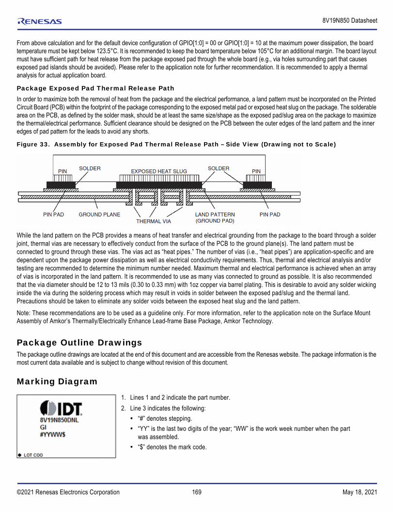
169©2021 Renesas Electronics Corporation May 18, 2021
8V19N850 Datasheet
From above calculation and for the default device configuration of GPIO[1:0] = 00 or GPIO[1:0] = 10 at the maximum power dissipation, the board temperature must be kept below 123.5°C. It is recommended to keep the board temperature below 105°C for an additional margin. The board layout must have sufficient path for heat release from the package exposed pad through the whole board (e.g., via holes surrounding part that causes exposed pad islands should be avoided). Please refer to the application note for further recommendation. It is recommended to apply a thermal analysis for actual application board.
Package Exposed Pad Thermal Release PathIn order to maximize both the removal of heat from the package and the electrical performance, a land pattern must be incorporated on the Printed Circuit Board (PCB) within the footprint of the package corresponding to the exposed metal pad or exposed heat slug on the package. The solderable area on the PCB, as defined by the solder mask, should be at least the same size/shape as the exposed pad/slug area on the package to maximize the thermal/electrical performance. Sufficient clearance should be designed on the PCB between the outer edges of the land pattern and the inner edges of pad pattern for the leads to avoid any shorts.
Figure 33. Assembly for Exposed Pad Thermal Release Path – Side View (Drawing not to Scale)
While the land pattern on the PCB provides a means of heat transfer and electrical grounding from the package to the board through a solder joint, thermal vias are necessary to effectively conduct from the surface of the PCB to the ground plane(s). The land pattern must be connected to ground through these vias. The vias act as “heat pipes.” The number of vias (i.e., “heat pipes”) are application-specific and are dependent upon the package power dissipation as well as electrical conductivity requirements. Thus, thermal and electrical analysis and/or testing are recommended to determine the minimum number needed. Maximum thermal and electrical performance is achieved when an array of vias is incorporated in the land pattern. It is recommended to use as many vias connected to ground as possible. It is also recommended that the via diameter should be 12 to 13 mils (0.30 to 0.33 mm) with 1oz copper via barrel plating. This is desirable to avoid any solder wicking inside the via during the soldering process which may result in voids in solder between the exposed pad/slug and the thermal land. Precautions should be taken to eliminate any solder voids between the exposed heat slug and the land pattern.
Note: These recommendations are to be used as a guideline only. For more information, refer to the application note on the Surface Mount Assembly of Amkor’s Thermally/Electrically Enhance Lead-frame Base Package, Amkor Technology.
Package Outline DrawingsThe package outline drawings are located at the end of this document and are accessible from the Renesas website. The package information is the most current data available and is subject to change without revision of this document.
Marking Diagram
1. Lines 1 and 2 indicate the part number.
2. Line 3 indicates the following:
“#” denotes stepping.
“YY” is the last two digits of the year; “WW” is the work week number when the part was assembled.
“$” denotes the mark code.
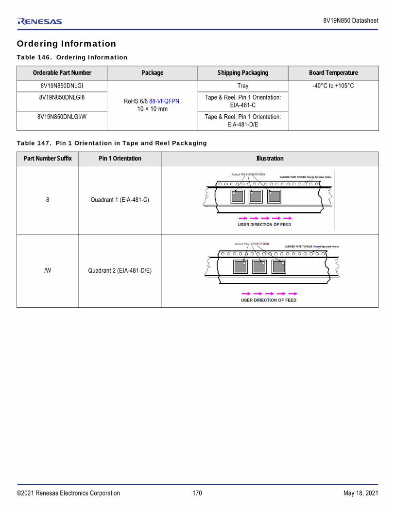
170©2021 Renesas Electronics Corporation May 18, 2021
8V19N850 Datasheet
Ordering Information Table 146. Ordering Information
Orderable Part Number Package Shipping Packaging Board Temperature
8V19N850DNLGI
RoHS 6/6 88-VFQFPN, 10 × 10 mm
Tray -40°C to +105°C
8V19N850DNLGI8 Tape & Reel, Pin 1 Orientation: EIA-481-C
8V19N850DNLGI/W Tape & Reel, Pin 1 Orientation: EIA-481-D/E
Table 147. Pin 1 Orientation in Tape and Reel Packaging
Part Number Suffix Pin 1 Orientation Illustration
8 Quadrant 1 (EIA-481-C)
/W Quadrant 2 (EIA-481-D/E)

171©2021 Renesas Electronics Corporation May 18, 2021
8V19N850 Datasheet
GlossaryTable 148. Abbreviations and Nomenclature
Abbreviation Description
Index n Denominates a clock input CLK_n. Range: 0 to 1
Index x Denominates a RF clock channel, clock and SYSREF outputs, clock frequency divider, delay circuits and the associated configuration bits. Range: R0, R1, R2, R3
Index y Denominates a QCLK RF-PLL output and associated configuration bits. Range: R0, R1, R2, R3, R4, R5
Index d Denominates a QCLK DPLL output and associated configuration bits. Range: D0, D1, D2, D3
Index r Denominates a QREF RF-PLL SYSREF output and associated configuration bits. Range: R0, R1, R2, R3, R4, R5
VDD_V Denominates voltage supply pins. Range: VDD_DPLL0, VDD_DPLL1, VDD_GPIO, VDD_APLL, VDD_RFPLL, VDD_RFVCO, VDD_DCO1, VDD_INP, VDD_SPI, VDD_OSC, VDD_XO, VDD_SYNC
VDDO_V Denominates voltage supply pins. Range: VDDO_QREF, VDDO_D0, VDDO_D1, VDDO_D2, VDDO_D3, VDDO_R01, VDDO_R23, VDDO_R4, VDDO_R5, VDDO_QR, VDDO_REF
status_condition Status conditions.
[...] Index brackets describe a group associated with a logical function or a bank of outputs.
… List of discrete values
Device clock Clock generated from the RF-PLL to drive converters (ADC, DAC). For converters, the device clock is a master clock signal from which a device must generate its local clocks.
SYSREF A periodic or continues, one-shot (strobe-type), or “gapped” periodic signal used to align the boundaries of local clocks in JESD204B/C subclass 1 devices. SYSREF output signals are synchronous with the device clock.
DPLL-0 with DCO-0, APLL-0
Functional unit of a digital PLL zero that contains a digitally controlled oscillator (DCO-0) and an analog PLL (APLL-0) for jitter attenuation and frequency conversion.
DPLL-1 with DCO-1, APLL-1
Functional unit of a digital PLL one that contains a digitally controlled oscillator (DCO-1) and an analog PLL (APLL-1) for jitter attenuation and frequency conversion.
APLL-2 Functional unit of an analog PLL 2, independently operating from other PLLs.
RF-PLL Functional unit of an analog PLL for RF frequency generation, independently operating from other PLLs.
SYS-APLL System analog PLL. Provides internal clock signals.
SYS-DPLL System digital PLL.
1PPS A 1Hz synchronization signal (one pulse per second)
FCW Frequency control word
TDC Time-to-Digital converter. Front-end of the DPLLs
PEC Phase Error Compensation
DSM or ΔΣ Delta-Sigma modulator
R/O Read-only register bit
R/W Register bit with read/write access
RW1C Register bit with read/write access, bit is cleared (reset to 0) by writing a “1”. Used for latched status bits
W1AC Register bit with write access and auto-clear
172©2021 Renesas Electronics Corporation May 18, 2021
8V19N850 Datasheet
Errata
Revision History
Table 149. Functional Errata
# Parameter/Function Description Work-Around
D1 tSCO - Clock in to Data Out (Slave)tHD_PP - SDA Signal Data Hold Time
Violations to I3C specification - see footnotes in Table 143
None.
D2 I3C/I2C Protocol After the device NACKs for any errors, the master should issue a stop and then do a start for continuing the transaction. A Repeat start after the NACK does not ACK for the continuing transactions.
Master needs to issue single START.
D3 I3C/I2C Protocol RSTDAA CCC - The slave does not respond to I2C after RSTDAA CCC instruction was sent.I2C does not respond after issuing the 7E address.
Not supported.
D6 Hitless switching and switching between low frequency clocks (< 1MHz).
When using hitless switching, for low frequency clocks (< 960kHz), larger than expect phase transient may be seen at the clock outputs. Worse case maximum is < 2.5ns.
To meet < 1ns, use clocks > 960kHz. AC/DC specification updated to reflect.
D7 Reference switching between 1PPS clocks. Reference switching (both normal and hitless) is not supported with 1PPS input clocks.
None.
Revision Date Description
May 18, 2021 Updated the following figures: – Figure 1– Figure in Table 6– Figure in Table 7– Figure 13– Figure 14
March 15, 2021 Corrected description of “Optimized for low phase noise” in Features and Features (Full List) Corrected several typos in Table 140
February 25, 2021 Updated the address offsets in Table 51
February 17, 2021 Clarified throughout document that operating temperature range is based on “board” temperature Clarified in all AC/DC Tables that 105oC is measured at case Corrected that APLL-0 VCO supports range of 2.45-2.58GHz Corrected default value for HITLESS_BW_SHIFT_DPLL0[4:0] and HITLESS_BW_SHIFT_DPLL1[4:0] Update Table 139 to add “Output Phase Change for Hitless Reference Switching” Added D6 and D7 to Erratum section Other minor text edits for clarification or to fix typos
January 21, 2021 Initial release.
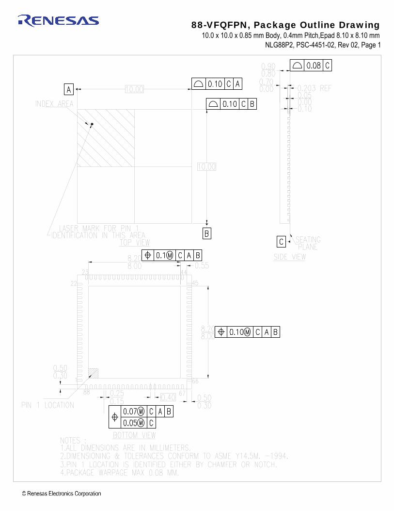
© Integrated Device Technology, Inc.
88-VFQFPN, Package Outline Drawing
10.0 x 10.0 x 0.85 mm Body, 0.4mm Pitch,Epad 8.10 x 8.10 mmNLG88P2, PSC-4451-02, Rev 02, Page 1

© Integrated Device Technology, Inc.
88-VFQFPN, Package Outline Drawing
10.0 x 10.0 x 0.85 mm Body, 0.4mm Pitch,Epad 8.10 x 8.10 mmNLG88P2, PSC-4451-02, Rev 02, Page 2
Description
Dec 4, 2017 Rev 01 New Format
Package Revision HistoryRev No.Date Created
March 8, 2018 Rev 02 Change QFN to VFQFPN, Change Pin 1 Identifier
Corporate HeadquartersTOYOSU FORESIA, 3-2-24 Toyosu,Koto-ku, Tokyo 135-0061, Japanwww.renesas.com
Contact InformationFor further information on a product, technology, the most up-to-date version of a document, or your nearest sales office, please visit:www.renesas.com/contact/
TrademarksRenesas and the Renesas logo are trademarks of Renesas Electronics Corporation. All trademarks and registered trademarks are the property of their respective owners.
IMPORTANT NOTICE AND DISCLAIMER
RENESAS ELECTRONICS CORPORATION AND ITS SUBSIDIARIES (“RENESAS”) PROVIDES TECHNICAL SPECIFICATIONS AND RELIABILITY DATA (INCLUDING DATASHEETS), DESIGN RESOURCES (INCLUDING REFERENCE DESIGNS), APPLICATION OR OTHER DESIGN ADVICE, WEB TOOLS, SAFETY INFORMATION, AND OTHER RESOURCES “AS IS” AND WITH ALL FAULTS, AND DISCLAIMS ALL WARRANTIES, EXPRESS OR IMPLIED, INCLUDING, WITHOUT LIMITATION, ANY IMPLIED WARRANTIES OF MERCHANTABILITY, FITNESS FOR A PARTICULAR PURPOSE, OR NON-INFRINGEMENT OF THIRD PARTY INTELLECTUAL PROPERTY RIGHTS.
These resources are intended for developers skilled in the art designing with Renesas products. You are solely responsible for (1) selecting the appropriate products for your application, (2) designing, validating, and testing your application, and (3) ensuring your application meets applicable standards, and any other safety, security, or other requirements. These resources are subject to change without notice. Renesas grants you permission to use these resources only for development of an application that uses Renesas products. Other reproduction or use of these resources is strictly prohibited. No license is granted to any other Renesas intellectual property or to any third party intellectual property. Renesas disclaims responsibility for, and you will fully indemnify Renesas and its representatives against, any claims, damages, costs, losses, or liabilities arising out of your use of these resources. Renesas' products are provided only subject to Renesas' Terms and Conditions of Sale or other applicable terms agreed to in writing. No use of any Renesas resources expands or otherwise alters any applicable warranties or warranty disclaimers for these products.
(Rev.1.0 Mar 2020)
© 2020 Renesas Electronics Corporation. All rights reserved.


