Embed Size (px)
Citation preview

.JT-j."/2 _' '"3
Radio Links for the NASA ABTS
Final ReportDean C. Jeutter
11 December 1996
Marquette University
Biotelemetry Laboratory
Radio Links for the NASA ABTS:
NASA University Consortium Grant REF# 96-108
Project Dates: 5 DEC 95 to 4 DEC 96
Contract # NCC2-5108
https://ntrs.nasa.gov/search.jsp?R=19980217139 2018-09-03T22:21:29+00:00Z

Goals
• Determine Out-Link FSK Bandwidth
• Develop FSK Outlink Transmitter
• Develop Wideband Outlink FSK Receiver
• Develop OOK In-Link Transmitter
• Develop OOK In-Link Receiver
• Marry Out-Link & In-Link Components
Outlink FSK Bandwidth preliminary inlink transmitter were
accomplished in Summer 1995 visit. The calculation of FSK
bandwidth is repeated in these notes. Spectrum analyzer
measurements of the actual FSK spectrum agree well with thecalculations.
• The goal to develop a wideband FSK receiver for outlink data was
given first priority for end of Summer 1996 completion.
The goal of developing OOK inlink transmitter and receiver system
components and interfacing all outlink and inlink components into an
operating closed loop prototypical system was given a December 1,
1996 completion date.
2
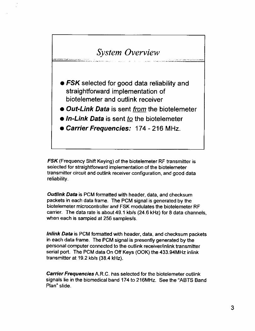
System Overview
• FSK selected for good data reliability and
straightforward implementation ofbiotelemeter and outlink receiver
• Out-Link Data is sent from the biotelemeter
• In-Link Data is sent to the biotelemeter
• Carrier Frequencies: 174 - 216 MHz.
FSK (Frequency Shift Keying) of the biotelemeter RF transmitter is
selected for straightforward implementation of the biotelemeter
transmitter circuit and outlink receiver configuration, and good datareliability.
Outlink Data is PCM formatted with header, data, and checksum
packets in each data frame. The PCM signal is generated by thebiotelemeter microcontroller and FSK modulates the biotelemeter RF
carrier. The data rate is about 49.1 kb/s (24.6 kHz) for 8 data channels,
when each is sampled at 256 samples/s.
Inlink Data is PCM formatted with header, data, and checksum packets
in each data frame. The PCM signal is presently generated by the
personal computer connected to the outlink receiver/inlink transmitter
serial port. The PCM data On Off Keys (OOK) the 433.94MHz inlink
transmitter at 19.2 kb/s (38.4 kHz).
Carrier Frequencies A.R.C. has selected for the biotelemeter outlink
signals lie in the biomedical band 174 to 216MHz. See the "ABTS BandPlan" slide.
3
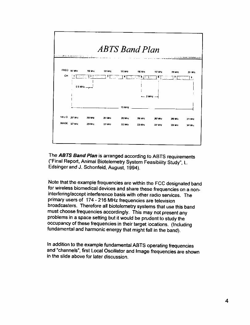
ABTS Band Plan
FREQ 187 MHz 189 MHz t91 MHz 193 MHz 196 MHz 197 MHz 199 MHz 201 MHz
i I
05 MHz _ i
_2MHz _
15MHz
1st k O : 257 MHz 2fi9 MHz 261 MHz 263 MHz 265 MHz 26? MHz 26_ MHz 271 MHz
IMAGE: 327 MHz 329 MHz 331 MHz 333 MHz 335 MHz 337 MHz 339 MHz 341 MHz
The ABTS Band Plan is arranged according to ABTS requirements
("Final Report, Animal Biotelemetry System Feasibility Study", L.Edsinger and J. Schonfeld, August, 1994).
Note that the example frequencies are within the FCC designated band
for wireless biomedical devices and share these frequencies on a non-interfering�accept interference basis with other radio services. The
primary users of 174 - 216 MHz frequencies are television
broadcasters. Therefore all biotelemetry systems that use this band
must choose frequencies accordingly. This may not present any
problems in a space setting but it would be prudent to study the
occupancy of these frequencies in their target iocations. (Including
fundamental and harmonic energy that might fall in the band).
In addition to the example fundamental ABTS operating frequencies
and =channels", first Local Oscillator and Image frequencies are shownin the slide above for later discussion.
4

Outlink Bandwidth Calculations
• Packet Rate
• Packet Length
• Baud Rate
• Signal Bandwidth
Packet Rate
Maximum 8 Data Channels + Header and Checksum = 256 Samples/sper channel
Packet Length
1 byte (header) + 16 bytes (data) + 1 byte (checksum) = 16bytes/packet
8 bits (data) + 2 bits (start & stop) = 10 bits/byte
18 bytes/packet X 10 bits/byte = 180 bits/packet
Baud Rate
180 bits/packet X 256 packets/s = 49.1 kb/s
The apparent data rate then is 24.6 kHz
Signal Bandwidth
BW = FMOD [ 213+ 1 ] (Carson's Theorem)
Choose Modulation Index = 5 (Allows 5 harmonics)
So signal BW = 24.6 kHz X 11 = 270 kHz
5

Out-Link Receiver Features
• Frequency coverage: 174- 216 MHz
• Synthesized: 0.01, 0.1, 1, 2 MHz steps
• Dynamic Range: BDR=67dB; IMD-DR=87dB
• MDS: -115 dBm (SINAD)
• I.F. Bandwidth: 280 kHz
• Outputs: PCM; RSSI; Detector; PLL; Squelch
• Compatibility with other biotelemetry systems
6

Receiver Block Diagrams
• Receiver RF Subsystem
• Microcontroller Subsystem
• Frequency Synthesizer
• Power Supplies and Audio Output
See following four slides
7

Receiver RF Subsystem
C Broadband
J Match
Image RejectionFilter
Voltage Tuned TuningVoltage
12442 6MHzF'rs"°I loo-HFrequency Voltage Controlled -= Converter
Synlhesize¢ Oscillator
I 80.TMHz.I I
Programming from I Wideband
Microcontrolier IIO FM IF Subsystem
Board _ Second I.F. Filter _ MC13158
FO = 10.7 MHz. _BW = 280 kHz
II I I I
Outputs _ Squelch RSSI PCM Data Detector
MMIC
I.F. Amplifier
1SAW
Band Pass Filter
Fe = 70 MHzBW = 280 kHz
IPLL Lock
8

Microcontroller
IFREQ: 194 010 MHz I ILCD CONTRAST I
L I Adj.=n.t IISTEP:,o,.z I I P°"_"e'°rII iquid Crystal Disp4ay
OlSPLAYLTCHES
I Octal D Flip-Flop
I ,MC68HC11E2FN
I Microcontroller
FREQUENCY SET
Opbcal Encoder
Subsystem
IN-LINK
Antenna
I IMAGE REJECTION
FILTER
Center Frequency
Tuning Potentiometer
AGC
Level Adjustment
Potentiorneter
_ FREQUENCY
PROGRAMMING
To Rlcelve¢
Board
J
I
10 mW MMIC TRANSMITTER RS-232 / to/from
Amplifier SAW AM Hybnd DRIVER/RECEIVER erso¢_l Computer
Note that the Image Rejection Filter tuning voltage and the AGC
(Automatic Gain Control) voltage can be readily provided by DAC's
(Digital to Analog Converter) under microcontroller supervision. In the
present receiver implementation these voltages are supplied by
potentiometers. The tuning voltage is buffered and available to external
preselector filter and preamplifier. This allows tuning the complete
system with just one frequency command input.
9

Frequency Synthesizer
1DLIALMCEKILUSDIVIDE _ PLLFREQUENCY H
BY40/41 PRESC,ALER SYNTI-EStZER LOOP FILTERMC12016 MC145152 LF3Sl
IFREQUENCY _NG I
INPUT FromMcrocollt_lerI/O Board
1From244 - 288 M-lz.
FirstL.Q
Volta_ ConUdledOscil_mor
PLLLOCK DETECTOR /
MC33171 p LOCK
To 244 - 288 MHz.First L.O.
VottageCo.oiledOscillator
The Frequency Synthesizer is of conventional design.
• The MC45152 PLL is a CMOS device and the MC12016 is a ECLdevice.
• The Loop Filter is a 3rd order filter that was designed and modeledusing PSPICE.
• An LF351 FET input operational amplifier is the active device in the filter.
• The PLL Lock Detector is a pulse integrator and comparator circuit usinga single supply operational amplifier for the active device. A PLL lockindication is provided by a green LED on the receiver's front panel.
• Loop Iockup time is about 10 ms for 2 MHz steps
The frequency programming procedure for the synthesizer is detailedin the following two slides.
10

Power Supplies and Audio Output
15- 28VDC =_
POWER INPUT
Power Consumption:
VIN = 15VDC
I_N= 280mA
P_N= 4.2W
Audio from FM IF
Subsystem !
12 VDC / Regulated 12VOC to Receiver RF
REGULATOR _I_ and Frequency SynthesizerSubsystems
5 VDC | Regulated 5VDC to Miorontrolle¢
REGULATOR _ Subsystem
I AUDIO VOLUME IPotentiocneter
1
i I
11

Frequency Programming Procedure
• Uses Motorola MC145152 PLL
• FRx = 174 to 216MHz and FIF = 70MHz
• FLo "" 244 to 286MHz
• 2-Modulus Prescaler with 40/41 Divide
• FSTEP= FREF = 10kHz
• Clock Divide Value = 1024 so
FXTAL= 10.240MHz
• MC145152 PLL has N and A registers
• Registers are loaded in parallel from two latches
• Total divide value = N T - N x P + A
• Nr = FLO / FSTEP = FLO/10kHz
• Use MC12106 ECL Divider with P = 40
Example: Let FRX= 195.09 so FLO = 265.09MHz
Step___!: Set A = 0:
NTOT = 265.090/0.010 = 26509
Nlo = 26509 / P = 26509 / 40 = 662.725
Step 2: Take Integer part of N10: Nlo = 662
Ste__3: Convert Nlo = 662 to binary:
N2 = 1010010110
Ste__4: Find A = NTo-r - N x P
Alo = 26509 - 662 x 40 = 29
Ste__5: Convert A10 = 29 to binary:
A z = 011101
Program Microcontroller to Generate N and A from
Optical Encoder Receiver Frequency Adjust
Step 7_
12

Synthesizer Design Spreadsheet
• Design Aid for PLL Programming
• Uses High-Side Local Oscillator Injection
• For Dual and Single Modulus Prescalers
• Enter Receiver Frequency Range,
Frequency Step Size, I.F., Prescale Value,Clock Divide Value
• Spreadsheet shows N and A Register
Programming values in Decimal and Binary
NASA ABTS RECEIVER - PLL PROGRAMMING
"" HIGH SIDE INJECTION *°°
Enter frequency step size, (Fatep) kHz : 10 Enter clock divide value (R), MHz: 1024
Enter Lowest input receive freq, (Frx) MHz: 174 Dual Modulus: (N and A Counters)
Freference, kHz = 10 000
Enter Highest input receive freq, (Frx) MHz: 216 Fxtel, MHz = 10.240
Fin max to PLL, kHz will be: 10 000
Enter Receiver I.F,, MHz: 70
Single Modulus: (N Counter Only)
Enter praacale value, (P): (0 = NONE) 40 Freference, kHz = 0.250
Fxtel. MHz = 0256
Enter TABLE (below) increment, kHz: 2000 Fin max to PLL. kHz will be: 7100.00
Manual Calculation: Enter Receive Frequency, MHz. = 190
I".........zj _o..... I...........oI .,o.,o...2 I" ...... I ...... I^°':el°l _b'"' II_tID.UU ZOO UUU ZOOUU 101 l 111UTUI 1UIU 0130 1UU11UUUI U 1UlU
H eCnlVe, MHZ
1#4,00
110.00
1/8.00
18000
162.00
184.00
100.00
100.00
lY0,00
102.00
lY4.00
lY§.00
1WeUU
20000
202.00
Z04.00
ZUO,UU
208.00
210,00
21zgu
2140U
214.UU
ZIO.UU
L.U., MHZ
244.000
240000
Z48.08U
200.000
252,000
254.000
Z00.guo
200.000
250.000
252.000
Z540UU
265.0U0
208.0U0
2rU,800
2/2 .UUU
2 f4 .UUU
2 rS.UUU
218.080
ZUU.OUU
ZeZUUU
ZnE.UU8
zn4.ugu
205.000
24400
24500
24800
23000
25200
25400
ZbSUU
20500
2§000
25200
25400
25§00
25800
Z/UUU
ZI2UU
z/4gg
Z/500
ZIUUU
28008
ZUZUU
20400
28400
ZB50U
10 NtOtnlDeSO 2
101111101010000
101111101010001
101111101010010
10111110101°011
101111101010100
181111101010101
181111101U10110
101111101010111
101111101011000
101111101011001
101111101011010
101111181011011
101111101011100
1011111U1011101
101111101811110
101111101011111
1011111011U0000
101111101100001
101111101100010
101111101100511
10111110110(1100
11011111011(1111
11011111011100(1
610
§20
5Zb
030
¢J_D
540
54_
550
5b5
55(I
555
§/0
5/5
08(1
50_
5WU
5_5
/on
100
/10
I10
110
10 N base 2
10011U0010
1001100010
10U1100UIU
108110(1018
180110(1010
1U0110U010
1001100010
1001100(110
1001100010
1001100010
1001100010
10011U0010
10(11180010
1001100010
1001100010
100110U010
100110°010
10011(10010
100110°°10
100110(1010
100110001(1
1U11001010
1°11001°11
A base 2
10
t_o101
110
111
lOgO
1001
1010
1011
1100
1101
1118
1111
10°Ug
10001
1UUIU
10011
1UIUU
lg_111
13

Receiver Performance Tests
• Blocking Dynamic Range
• Intermodulation Distortion and 31P
• S+N+D and N+D
• 1st & 2nd Conversion Image Responses
• Mixer Spurs
• 1st & 2nd IF Rejection
• RSSI vs Signal Input Level
Each of these Receiver Performance Tests are detailed in the
following slides and notes.
14
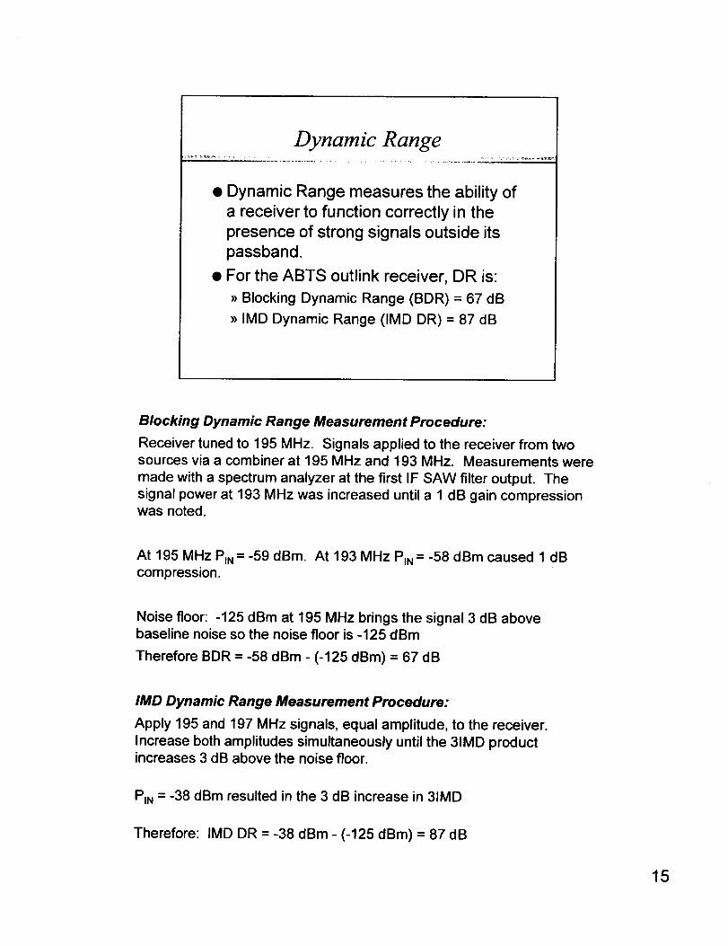
Dynamic Range
• Dynamic Range measures the ability of
a receiver to function correctly in the
presence of strong signals outside its
passband.
• For the ABTS outlink receiver, DR is:
)) Blocking Dynamic Range (BDR) = 67 dB
>>IMD Dynamic Range (IMD DR) = 87 dB
Blocking Dynamic Range Measurement Procedure:
Receiver tuned to 195 MHz, Signals applied to the receiver from twosources via a combiner at 195 MHz and 193 MHz. Measurements were
made with a spectrum analyzer at the first IF SAW filter output. The
signal power at 193 MHz was increased until a 1 dB gain compressionwas noted.
At 195 MHz P0N = -59 dBm. At 193 MHz PIN = -58 dBm caused 1 dBcompression.
Noise floor: -125 dBm at 195 MHz brings the signal 3 dB abovebaseline noise so the noise floor is -125 dBm
Therefore BDR = -58 dBm - (-125 dBm) = 67 dB
IMD Dynamic Range Measurement Procedure:
Apply 195 and 197 MHz signals, equal amplitude, to the receiver.
Increase both amplitudes simultaneously until the 31MD productincreases 3 dB above the noise floor.
PIN = -38 dBm resulted in the 3 dB increase in 31MD
Therefore: IMD DR = -38 dBm - (-125 dBm) = 87 dB
15

Intermodulation Distortion
IMD = 39 dB
I2F1-F 2 F_ F 2
-39dBm
-78dBm
Intermodulation Distortion occurs when a strong signal nearby in
frequency to the desired signal combines with the desired signal to
generate unwanted products (especially those close-by the desired
signal frequency) that can cause interference. It is the non-linear
operation of amplifiers, etc. that cause generation of IMD products.
The "close-in" unwanted signals are called the third order distortion
products or 31MD. They occur at 2XF 2 - F 1 and 2XF 1 - F 2
The results shown in the slide above were obtained by applying equal
amplitude unmodulated carriers (-40dBm) simultaneously to the
receiver from two signal sources combined with a 2-way, 0 o combiner
(Mini-Circuits ZSC-1, 4db insertion loss). F1 was 195 MHz and F2 was
197 MHz with 31MD products at 193 and 199 MHz. Second order
responses at 390, 394, 784, and 4 MHz were not significant.
A figure of merit for IMD is the 3rd order intercept point (30IP). It wascalculated from the 31MD measurements as follows:
rt X PA - PIMn
n-1
16

At 193 MHz:
]P3-3xPv,-Pi93 -117+75= --21 dBm
3-1 2
At 199 MHz:
ip 3 = 3xPFI -Pis_ = -117+78 --19.5 dBm3-1 2
Measurements were made at the first mixer input using a Tektronix
495P Spectrum Analyzer.
17

S+N+D and N+D
S+N+D and N+D vs. Input Signal Level5
m•0 0 ......
-5
_+ -10 .........
+a -25 .......
_ -35 : .......... i
I I
RF Input Signal Level, dBm
S+N+D
N+D
F0= 194MHz
FOEv= _125kHz
FMOo = lkHz
IF BW (3dB) = 280kHz
Procedure for S+N+D Measurement:
Apply 194MHz FM signal with 125kHz deviation, lkHz sine
baseband to the receiver. Measure S+N+D voltage (rms) at the
detector output as P_N is increased from -127 dBm.
Procedure for N+D Measurement:
Apply 194MHz unmodulated signal to the receiver. Measure
S+N+D voltage (rms) at the detector output as P_N is increasedfrom -127 dBm.
Minimum Detectable Signal (MDS):
One measure of MDS is the input power (dBm) where the S+N+D
is 3dB (i.e.: twice) the N+D. From the data:
MDS = -115 dBm
S+N+D and N+D detector output voltage measurements were made
with a HP-311A Audio Distortion Analyzer.
17

First Conversion Image Response
,' I
7O
F_F
70 MHz
_95 265
Fo FLo
70 MHz
335 F. MHz
FBG
With high-side injection of the first L.O. the First IF is:
FIFI=IFo-FLml =I195-265j=70MHz (FLm>F o)
The important Image Frequency is:
FIM G = F o + 2 x FIF 1 = 195 + 2 x 70 = 335 MHz
Measured Image Rejection Procedure:
Apply F o at Po then FIM G at PIMG to the Receiver Input
Output Reference" -50 dBm at the 70 MHz SAW I.F. Output
Results:
At F o = 195 MHz
At FIM G = 335 MHz
Po was -105 dBm
PIMG was -32 dBm
Therefore the Measured Image Rejection = Po" PIMG = -73 dB
See the "ABTS Band Plan" slide for complete Image frequency data
18

Second Conversion Image Response
/_)htude J_ 10.7 k//tz
J
107 70
F_2 F,_
,, -- 10.7 MI4z -_---.J
80.1 91.4 F, MHz
FLo_ F,um
With high-side injection of the second L.O. the Second IF is:
F=F2= I Fro1 - FLo2 J= J70 - 80.7 J = 10.7 MHz (FLo 2 > Fro1 )
The important Image Frequency is:
FIM G = FIF1 + 2 x FIF 2 = 70 + 2 x 10.7 = 91.4 MHz
Measured Image Rejection Procedure:
Apply FIF 1 at PZF1then FLO 2 at PLO2 to the Receiver Input
Output Reference: -60 dBm at the 10.7 MHz I.F. Amplifier Output
Results:
At FIF 1 = 70 MHz
At FIF 2 - 91.4 MHz
PIF1 was -105 dBm
PIF2 was -32 dBm
Therefore the Measured Image Rejection = PIFJ - PIF2 - -73 dB
19

Receiver Spur Analysis
input Center Frequency (195.00):195.00 BW (42.000):42.000
Output Center Frequency (70.000): 70.000 BW (0.5000):0.5000
Fixed or Variabia LO (V): V Frequency InversionLO Center Frequency (265): 265.00 BW (42.000): 42.000
Model Highest Harmonic: |nput(9): 9 LO (9): 9EXAMPLE: Frequency Steps: Input (21): 21 LO (21): 21RF=-10dBm
LO=+10dBm SPURS vl.01 - Kirt Blattenberger 1992
• LO " (-dBc)
0 1 2 3 4 S 6 7 II 90
1 OO2 69
3 5O
R 4F 5
6
• 78
9
# Cases Tasted: 193600
66
63 6974
72 77
83 8377
Tuesday lS Juf 1996 10:14:20 AM
Spurious Response analysis identifies the frequencies and
approximate levels of spurious signals that might be generated by thefirst mixer. This analysis aids in the choice of first IF frequency. Thetable shows acceptable spur levels for a 70 MHz IF for the receiver.
20

Receiver LF. Rejection
• Measured First I.F. Rejection:
• Measured Second I.F. Rejection:
Measured First LF. Rejection Procedure:
Apply F o at Po then FIF 1 at PIF1 to the Receiver Input
Output Reference: -50 dBm at the 70 MHz SAW I.F. Output
Results:
At Fo = 195 MHz
At FjF1 = 70 MHz
Po was -105 dBm
PtF1 was -7 dBm
Therefore the Measured First LF. Rejection = PIF1 - PIF2 = -98 dB
Measured Second LF. Rejection
Apply Fo at Po then FIF 2 at PIF2 to the Receiver Input
Output Reference: -60 dBm at the 10.7 MHz I.F. Amplifier Output
Results:
At Fo = 195 MHz
At FIF2 = 10.7 MHz
Po was -105 dBm
PIF2 was > 0 dBm
Therefore the Measured Second I.F. Rejection = Po - PtF2 > -105 dB
21

RSSI
RSSI Output Voltage vs. Signal Input Level
3
2.6 i i_iiii_i _> 2,4
_ 2,2
> 1.81.6
_ 1.41.2
1
"T "T _,
Signal Input Level, dBm
RSSI Dynamic Range:
The approximately linear RSSI range is -120 dBm to -40 dBm
so the RSSI Dynamic Range is 80 dB
RSSI Sensitivity:
The RSSI Sensitivity is the slope of the RSSI Output Voltage vs. Signal
Input Level curve:
Sensitivity = 1.7V / 80dB = 21.25 mV per dB
22

Receiver I/O Signals for External Use
• PC Control
• Detector Output
• RSSI Output
• Conditioned PCM Data
• Squelch
• PLL Lock Indication
PC Control provides I/O in RS-232 format via a rear apron DB-9 connector.
This is presently configured for connection to a personal computer forreceiver control and biotelemeter programming and for display of decoded
physiologic signals. The enabling software is a WINDOWS application
designed by J. Carter.
Detector output provides a voltage proportional to a biotelemeter frequency
variation from a programmed frequency. In the event that a biotelemeter
slowly drifts after implant this signal can be used to retune the outlink
receiver (within an established range).
RSSI output is a voltage that indicates the strength of the received
biotelemeter signal. It could be used in conjunction with other received data
parameters to suggest animal activity; it is an immediate indication of a
signal dropout. It also provides a demodulated AM output for potential usewith biotelemeters of other manufacture.
Conditioned PCM data is the data presented to the inlink transmitter.
Squelch is a high (carrier strength acceptable_ or low (carrier too weak)
voltage determined by an adjustable threshold. It is useful for disabling
external circuits so that they are not presented with noise.
PLL Lock indication is a voltage (High or Low) that reveals the lock status
of the PLL in the frequency synthesizer.
23

Receiver Usability with Other
Biotelemetry Systems
• Frequency Coverage 174 to 216 MHz
• PCM Data Output from FSK:
>>Buffered Raw data from FM Detector
>>Personal Computer Formatted (RS-232)
• PCM Data Output from PAM:
>>Buffered Raw Data from RSSI
>>Data BW = 3 kHz
The receiver design provides the flexibility for operation with a variety of
FSK, FM, and AM biotelemeters using PCM, PIM, PPM, etc. pulse
formatted time multiplexed encoding.
24

Team Involved
• Marquette University -
)) Andrea Biegel - Research Assistant
)) Aaron Jeutter - Receiver Micro Programmer
)) Dean Jeutter - RF Circuit Design
• Triomed Electronics -
)) Jerry Carter - WINDOWS GUI PC Software
)) Mark Geisler - Software Development for theBiotelemeter Microcontroller
25

Next Steps
• Summary: A functional Closed Loop
prototype demonstrates the feasibility of the
ABTS approach.
• Future:
_ Habitat/Glove box/Centrifuge projects
_ Biotelemetry System
_ Needed from ARC Group
Summary:
The closed loop prototype has operational bi-directional wireless links.The Wideband PCM-FSK receiver has been designed and
characterized. Now that both links function, communication
performance can be addressed. For example, noise problems with the
received outlink signal that caused the PC program to Iockup were just
recently revealed and minimized by software "enhancements" to the
Windows based PC program.
A similar problem with inlink communication was uncovered several
days before this report: A noise spike or dropout (expected events in
the animal Habitat) caused an interrupt to the implant microcontroller
which halted outlink transmission. Recovery of outlink transmission did
not reliably occur. The problem has been defined and implant software
is being modified to better recognize noise from data by changing the
timing associated with valid data packet identification and by better
utilizing the error flags generated by the microcontroller's SCI circuits.
Excellent inlink performance will also require improvements in the
implant's receiver. The biggest performance improvement can be
provided by antenna design for the Habitat. The quarter wavelength
whip antennas used with the demo prototype inlink leave much to bedesired.
Future: See Next Three Slides
26


Hab itat,
Future."
Glovebox, Centrifuge
• Install system in a Habitat, Glove box,
centrifuge project
)> Parallel activities at both ARC and MU
using identical systems
>_ Interface RF subsystems with targetenclosures' antennas
• Use appropriate enclosure antennas
(e.g.: Dr. Philip Carter designs)
• An efficient approach to adapting the ABTS to the Habitat, Glove box,
centrifuge project enclosures can be to provide MU with enclosures and
antennas and at the same time provide ARC with ABTS components.
• The PCM-FSK receiver was design with a 50 Ohm broadband input.
This was done to facilitate easy matching with an external low noise
preamplifier and Habitat antenna (Dr. Carter's design). The preamplifier
should have a preselector filter matched to the Habitat antenna. The
preselector filter can be voltage tuned by the tuning voltage provided at
the PCM-FSK receiver output connector. The addition of such a
preamplifier can improve overall receiver performance (noise, IMD,
dynamic range). Further, with the preamplifier located in close
proximity to the Habitat antenna, and with a 50 Ohm coaxial connection
to the remotely situated PCM-FSK receiver, overall receiver
performance is expected to be excellent.
• The interfacing of the inUnk RF with enclosure antenna(s) should beconsidered soon. The best situation would have one common antenna
serving both inlink and outlink. This might require the development of
duplexing circuits.
27

Future." Biotelemetry System
• Biotelemeter
• Outlink Receiver
• Inlink Transmitter
• Inlink Receiver
Biotelemeter
• Prune PCM frame, compress PCM data, and implement new
microcontroller (Microchip Corp. PIC Processor) for decreasedbiotelemeter power consumption
• Finalize implant RF transmitter- minimize power
• Crystal control the implant's transmitter. The CTS-Marden CrystalManufacturing Co. (Burlington, WI) was contacted recently to discuss
the possibility of fabricating a very miniature quartz crystal withfundamental oscillating frequencies available in the 174 - 216 MHz.
biotelemetry band. Such a crystal would lend frequency stability (vs.temperature and battery voltage) to the implant's transmitted signal.Reactance modulation would provide the needed FSK.
Interface with outlink and inlink antennas
Finalize modular approach to physiologic experiment flexibility
Begin plans for miniaturization and packaging
Outlink Receiver
• Add DAC's for automatic outlink receiver Image Rejection Filtertuning and for AGC control by receiver microcontroller
• These additions will be made in conjunction with a differentmicrocontroller having more I/O ports including two serial ports (suchas Motorola MC68HC12 or Phillips P51XA)
28

Future." Needed from ARC Group
• ABTS interface specifications
• System Decisions:
)) Antennas
)) Receivers
)) Receiver Multiplexing
• Habitat/Glovebox/Centrifuge Test Fixture
• Identify 1 or 2 initial physiology experiments
AB TS interface specifications
• Local and/or PC control? PC-104?
• Volume, cc; Ambient temperature; Vibration, etc.?
• Power available?
System Decisions
• Antennas for Biotelemeter Outlink and Inlink
• Number of outlink receivers per habitat?
• RF Multiplexing required?
Habitat / Glovebox / Centrifuge Test Fixture
• Configuration of Habitat outlink receivers and inlink transmitter
• Separate receiver boxes .
Identity One or Two Initial Physiology Experiments
• To set a goal for an initial trial
• Type, number of biomedical signals
• Sequencing time per animal
• Where will all that data go?
29

Inlink Transmitter
• Improve design for communication in Habitat (increase power?)
Inlink Receiver
• Sensitivity improvements depend largely on design of biotelemeterand Habitat antennas and inlink transmitter power. Communication
software improvements in the implant's software will continue.
3O