Embed Size (px)
Citation preview

National Aeronautics and Space Administration
Rad-Hard Structured ASIC Body of Knowledge
Jason Heidecker Jet Propulsion Laboratory
Pasadena, California
Jet Propulsion Laboratory California Institute of Technology
Pasadena, California
JPL Publication 13-11 7/13

i
National Aeronautics and Space Administration
Rad-Hard Structured ASIC Body of Knowledge
NASA Electronic Parts and Packaging (NEPP) Program
Office of Safety and Mission Assurance
Jason Heidecker Jet Propulsion Laboratory
Pasadena, California
NASA WBS: 104593 JPL Project Number: 104593 Task Number: 40.49.01.12
Jet Propulsion Laboratory 4800 Oak Grove Drive Pasadena, CA 91109
http://nepp.nasa.gov
ii
This research was carried out at the Jet Propulsion Laboratory, California Institute of Technology, and was
sponsored by the National Aeronautics and Space Administration Electronic Parts and Packaging (NEPP) Program.
Reference herein to any specific commercial product, process, or service by trade name, trademark, manufacturer, or
otherwise, does not constitute or imply its endorsement by the United States Government or the Jet Propulsion
Laboratory, California Institute of Technology.
©2013. California Institute of Technology. Government sponsorship acknowledged.

iii
TABLE OF CONTENTS 1.0 Introduction ........................................................................................................................................................... 1
2.0 Sandia National Laboratories: ViArray .................................................................................................................. 2 2.1.1 Performance Specs and Radiation Characterization ......................................................................... 2 2.1.2 Flight Heritage ................................................................................................................................... 3 2.1.3 Design Tools ..................................................................................................................................... 3 2.1.4 Design Security ................................................................................................................................. 4 2.1.5 Contact .............................................................................................................................................. 4
3.0 Honeywell: HX5000 ............................................................................................................................................... 5 3.1.1 Performance Specs and Radiation Characterization ......................................................................... 5 3.1.2 Flight Heritage ................................................................................................................................... 5 3.1.3 Design Tools ..................................................................................................................................... 5 3.1.4 Design Security ................................................................................................................................. 6 3.1.5 Contact .............................................................................................................................................. 6
4.0 Triad: VCA ............................................................................................................................................................ 7 4.1.1 Performance Specs and Radiation Characterization ......................................................................... 7 4.1.2 Flight Heritage ................................................................................................................................... 7 4.1.3 Design Tools ..................................................................................................................................... 7 4.1.4 Design Security ................................................................................................................................. 8 4.1.5 Contact .............................................................................................................................................. 8
5.0 Aeroflex ................................................................................................................................................................. 9
6.0 Conclusion .......................................................................................................................................................... 10
7.0 References .......................................................................................................................................................... 11

1
1.0 INTRODUCTION Structured Application-Specific Integrated Circuit (ASIC) technology is a platform between traditional ASICs and Field-Programmable Gate Arrays (FPGA). The motivation behind structured ASICs is to combine the low non-recurring engineering costs (NRE) costs of FPGAs with the high performance of ASICs.
FPGA technology is designed and fabricated in a process that is completely independent of end-user applications. It is a “one size fits all” approach to providing a programmable circuit that can support many applications. Because the customer has no involvement in FPGA development, there is no NRE cost to the customer. Moreover, because FPGAs are programmable (and some reprogrammable) by the end-user, FPGAs offer maximum flexibility in terms of programming, debugging, and prototyping. However, the routing complexity required to facilitate this flexibility comes at a large price in terms of the speed and performance achievable with an FPGA.
ASICs, on the other hand, are designed and developed with the end user’s application fully in mind. The ASIC is built to support only a single application, and is therefore a one-off development activity for the manufacturer. NRE costs are very high, as entirely new mask sets must be developed to support just a single customer’s needs. In contrast, with the FPGA, every chip is identical. However, because back-end development of an ASIC is done with a single customer’s application in mind, much higher speed and performance is achievable, as routing can be fully optimized for the customer’s specific application.
Structured ASICs aim to offer an intermediate solution. Structured ASICs have essentially the same structure as an FPGA, but they are mask-programmable instead of field-programmable. The manufacturer, therefore, goes through a single design and development activity to produce a structured ASIC platform, then finalizes the chip for each customer through a relatively simple programming step at the end. It follows that some interaction between the manufacturer and customer is required to produce the final circuit, which means more NRE than an FPGA but much less than an ASIC. Structured ASIC programming involves actual fabrication process steps that configure via layers between metal layers to produce the desired circuit. The routing complexity needed is much less than what is required for full field-programmability, so much greater speeds and performance are possible.
This report provides an overview of the structured ASIC platforms that are radiation-hardened and intended for space application.

2
2.0 SANDIA NATIONAL LABORATORIES: VIARRAY Sandia’s structured ASIC product line, known as “ViArray,” debuted in 2005 with the VA260 digital platform. The ViArray process was originally developed for nuclear weapon applications in a harsh radiation environment, making it ideal for space applications. The VA260 was implemented in Sandia’s 0.35 μm radiation-hardened SOI CMOS, 3.3 V technology. The platform offered 260K logic gates, 354 Kb of SRAM, 352 Kb of ROM, an on-chip oscillator, and 170 configurable I/Os.
Figure 2.0-1. Sample chips of Sandia’s Eiger (digital) and Whistler (mixed-signal) structured ASIC platforms [1].
The ViArray product line quickly moved away from VA260 in 2007 with the announcement of the Eiger (digital) and Whistler (mixed-signal, 2009) platforms (see Figure 2.0-1). The baseline process behind these platforms is also the radiation-hardened 3.3 V, 0.35 μm SOI CMOS. It has advanced significantly since the VA260 days and now supports 24 mask levels, SOI substrate, STI hardened field oxide, nitride trench capacitors, LDD implants, 7 nm tunnel oxide thickness, poly SEU transistors, titanium silicide, tungsten via fills, metal/metal capacitors, and LEFF of 0.28 μm (VT ~0.7 V and 1.0 V).
In addition to the Eiger and Whistler platforms, Sandia also offers ViArray embedded in custom ASICs. Beginning in 2012, 3D-ViArray (stacked chips) went into development to bring more performance in a smaller package/footprint. So far, all ViArray chips have been in plastic BGA packages. However, Sandia has started development on ceramic column grid arrays, flip-chip PBGA, and flip-chip on-board technologies.
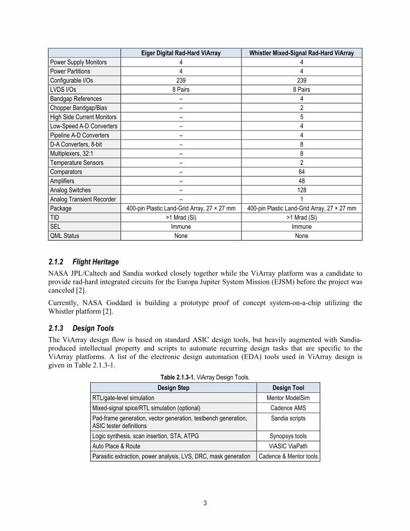
2.1.1 Performance Specs and Radiation Characterization A comparison of the Eiger and Whistler platforms, including radiation performance, is given in Table 2.1.1-1.
Table 2.1.1-1. Sandia Rad-Hard Structured ASIC Platforms. Eiger Digital Rad-Hard ViArray Whistler Mixed-Signal Rad-Hard ViArray
Process 0.35 μm SOI CMOS 0.35 μm SOI CMOS VDD 3.3 V 3.3 V Operating Temperature −55°C to 125°C −55°C to 125°C ASIC gate-equivalent 276K 138K Dual-Port SRAM 368 Kb 184 Kb Configurable ROM 384 Kb 192 Kb Volatile Memory 2 Kb – Oscillators 4 2 Phase Lock Loops 4 2
3
Eiger Digital Rad-Hard ViArray Whistler Mixed-Signal Rad-Hard ViArray Power Supply Monitors 4 4 Power Partitions 4 4 Configurable I/Os 239 239 LVDS I/Os 8 Pairs 8 Pairs Bandgap References – 4 Chopper Bandgap/Bias – 2 High Side Current Monitors – 5 Low-Speed A-D Converters – 4 Pipeline A-D Converters – 4 D-A Converters, 8-bit – 8 Multiplexers, 32:1 – 8 Temperature Sensors – 2 Comparators – 64 Amplifiers – 48 Analog Switches – 128 Analog Transient Recorder – 1 Package 400-pin Plastic Land-Grid Array, 27 × 27 mm 400-pin Plastic Land-Grid Array, 27 × 27 mm TID >1 Mrad (Si) >1 Mrad (Si) SEL Immune Immune QML Status None None
2.1.2 Flight Heritage NASA JPL/Caltech and Sandia worked closely together while the ViArray platform was a candidate to provide rad-hard integrated circuits for the Europa Jupiter System Mission (EJSM) before the project was canceled [2].
Currently, NASA Goddard is building a prototype proof of concept system-on-a-chip utilizing the Whistler platform [2].
2.1.3 Design Tools The ViArray design flow is based on standard ASIC design tools, but heavily augmented with Sandia-produced intellectual property and scripts to automate recurring design tasks that are specific to the ViArray platforms. A list of the electronic design automation (EDA) tools used in ViArray design is given in Table 2.1.3-1.
Table 2.1.3-1. ViArray Design Tools. Design Step Design Tool
RTL/gate-level simulation Mentor ModelSim Mixed-signal spice/RTL simulation (optional) Cadence AMS Pad-frame generation, vector generation, testbench generation, ASIC tester definitions
Sandia scripts
Logic synthesis, scan insertion, STA, ATPG Synopsys tools Auto Place & Route ViASIC ViaPath Parasitic extraction, power analysis, LVS, DRC, mask generation Cadence & Mentor tools

4
2.1.4 Design Security FPGAs have a distinct advantage over ASICs (and structured ASICs) in terms of design security. Since FPGAs are field-programmable by the end-user, the application design does not need to be shared with a third party (the manufacturer). However, by using a trusted vendor, security risks can be mitigated.
Sandia is a DoD Category 1A Accredited Supplier of both “trusted design and foundry services” with ISO 9001 certified process optimized for custom radiation-hardened, digital, analog, and mixed-signal ASICs.
2.1.5 Contact Michael Holmes Manager – Mixed Signal ASIC/SoC Products Sandia National Laboratories 1515 Eubank Blvd. SE MS-1072 Albuquerque, NM 87123 Office: 505-284-9673

5
3.0 HONEYWELL: HX5000 The HX5000 standard cell, structured ASIC platform went into production in 2007 and received QML Class Q qualification in 2008 [3].
HX5000 is a digital platform built on Honeywell’s S150 process, a 1.8 V, 0.15 μm SOI CMOS technology. HX5000 provides more than 15M usable gates and supports up to 1000 signal I/Os.
3.1.1 Performance Specs and Radiation Characterization Table 3.1.1-1. Honeywell HX5000 Performance Specs and Radiation Characterization.
HX5000 (Digital) Process 0.15 μm SOI CMOS Operating Temperature −55°C to 125°C VDD 1.8 V Signal I/O 1000 ASIC gate-equivalent 15M Package Ceramic LGA or QFP TID >1 Mrad (Si) SEL Immune QML Status Class Q
3.1.2 Flight Heritage Honeywell has delivered over 700 ASIC designs on their HX2000, HX3000, and HX5000 process lines. The percentage of these designs that are on the HX5000 standard cell/structured array process is unknown.
3.1.3 Design Tools Honeywell utilizes the Synopsys Pilot design flow/environment and Mentor tool set, including:
• Design Compiler • PrimeTime SI • PrimeTime PX • Formality • TetraMAX • IC Compiler • StarRCXT • VCS • Mentor ModelSim • Mentor Tessent M-BIST
Honeywell-provided VDS-VI tools:
• IOGen • Verify • SpecBuilder/TestSpec • Test Collar

6
3.1.4 Design Security Honeywell Aerospace Plymouth is a Category 1A trusted source with accreditation of trust from the Defense Microelectronics Activity (DMEA) as defined by Instruction 8500.2 of the Department of Defense Directives.
3.1.5 Contact Thomas Romanko, Microelectronics Application Engineer Honeywell Microelectronics 1200 Highway 55 Plymouth, MN 55441 Office: 763-954-2103

7
4.0 TRIAD: VCA Triad is currently in development on radiation-hardened mixed-signal structured ASICs using their patented via-configurable array (VCA) technology, which is based on ViASIC (acquired by Triad in 2011) ViaMask technology [4]. ViASIC used the base technology in high volume commercial applications since 2000. Now Triad is working on using radiation-hardened-by-design (RHBD) techniques to take the product to the military/space market.
Similar to Sandia, Triad offers two platforms: mixed signal and purely digital. The mixed-signal platform is known as “VCA-301” and the six digital platforms are numbered from “VCA-501” thru “VCA-506.”
4.1.1 Performance Specs and Radiation Characterization Table 4.1.1-1 gives a comparison between the VCA-201 mixed signal platform and the VCA-501 digital platform from Triad. The differences among the six digital platforms are given in Table 4.1.1-2.
Table 4.1.1-1. Triad Rad-Hard Structured ASIC Platforms. VCA-301
Mixed Signal VCA-501 Digital
Process 0.18 µm CMOS IBM 9LP 90 nm CMOS Operating Temperature −55°C to 125°C −55°C to 125°C Voltage 1.8 or 3.3 V 1.2 V, 1.2–2.5 V I/O TID >300 krad (Si) >1 Mrad (Si) Gates 28K >1M SEU <1e−5 errors/day <1e−5 errors/day SEL Immune Immune
Table 4.1.1-2. Triad Digital Platforms.
Array Gates Distributed RAM Block RAM VROM SERDES VCA-501 107k 78 kb – 288 kb – VCA-502 177k 129 kb 5× 8k×8 288 kb 4 ch VCA-503 239k 213 kb – 288 kb – VCA-504 490k 356 kb 8× 8k×8 288 kb 8 ch VCA-505 225k 164 kb 32× 8k×8 288 kb – VCA-506 1.17M 848 kb 12× 8k×8 288 kb 16 ch
4.1.2 Flight Heritage None yet. Technology is still under development although prototype chips have undergone TID and SEE testing. Production/flight products are expected late 2013.
4.1.3 Design Tools One of the biggest selling points for Triad is their ViaDesigner and ViaPath design tools, which promises very rapid ASIC development. With ViaDesigner, you design and simulate your design using high-level resources. ViaPath is then the automatic place and route software that maps your design to a VCA.

8
4.1.4 Design Security Triad’s foundry partner is austriamicrosystems (ams), headquartered in Graz, Austria. This is also where their foundry is located, so space programs with requirements for US-trusted foundries may have an issue with this. ams also partners with UMC (Taiwan), TSMC (Taiwan), IBM (US), OKINS (Philippines), FCI (Singapore), Amkor (US/Japan/Philippines), and Carsem (Malaysia) for foundry, test, and assembly services. With so many entities involved in the design, production, and test of the structured ASIC chip, maintaining design security could be an issue.
4.1.5 Contact Jim Kemerling, CTO Triad Semiconductor, Inc. 3900 Westpoint Blvd Ste D Winston-Salem, NC 27103 Office: 336-774-2150
9
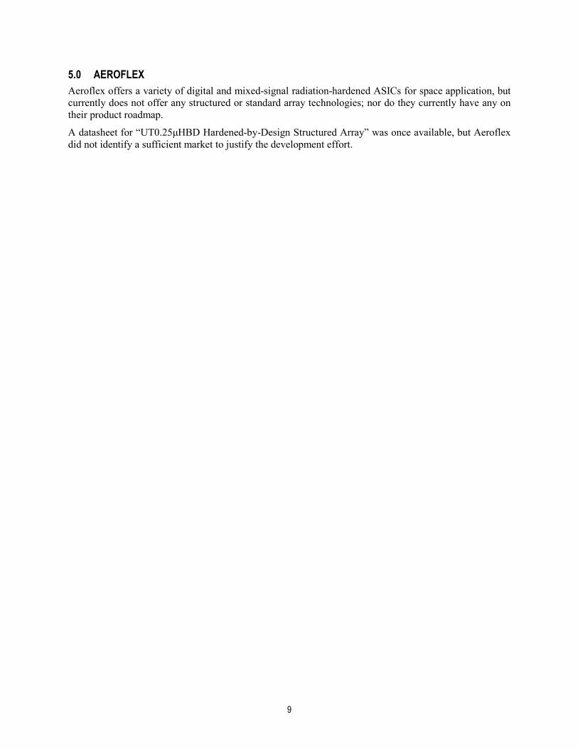
5.0 AEROFLEX Aeroflex offers a variety of digital and mixed-signal radiation-hardened ASICs for space application, but currently does not offer any structured or standard array technologies; nor do they currently have any on their product roadmap.
A datasheet for “UT0.25μHBD Hardened-by-Design Structured Array” was once available, but Aeroflex did not identify a sufficient market to justify the development effort.
10
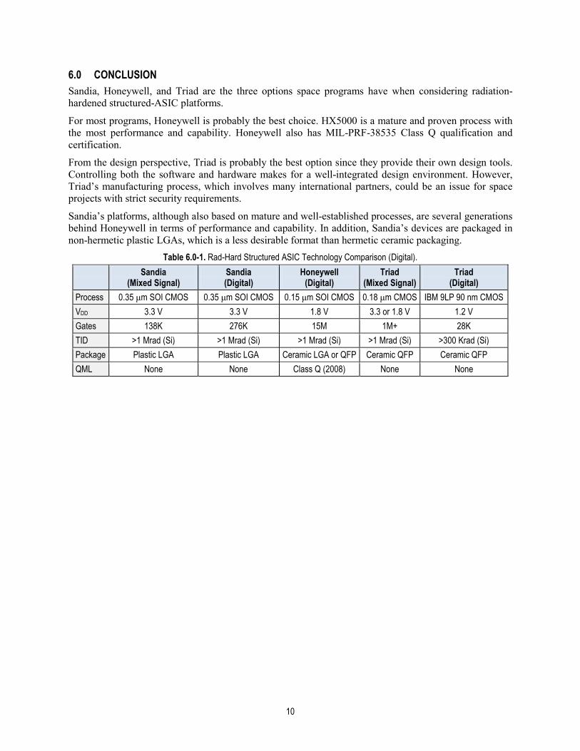
6.0 CONCLUSION Sandia, Honeywell, and Triad are the three options space programs have when considering radiation-hardened structured-ASIC platforms.
For most programs, Honeywell is probably the best choice. HX5000 is a mature and proven process with the most performance and capability. Honeywell also has MIL-PRF-38535 Class Q qualification and certification.
From the design perspective, Triad is probably the best option since they provide their own design tools. Controlling both the software and hardware makes for a well-integrated design environment. However, Triad’s manufacturing process, which involves many international partners, could be an issue for space projects with strict security requirements.
Sandia’s platforms, although also based on mature and well-established processes, are several generations behind Honeywell in terms of performance and capability. In addition, Sandia’s devices are packaged in non-hermetic plastic LGAs, which is a less desirable format than hermetic ceramic packaging.
Table 6.0-1. Rad-Hard Structured ASIC Technology Comparison (Digital). Sandia
(Mixed Signal) Sandia (Digital)
Honeywell (Digital)
Triad (Mixed Signal)
Triad (Digital)
Process 0.35 μm SOI CMOS 0.35 μm SOI CMOS 0.15 μm SOI CMOS 0.18 μm CMOS IBM 9LP 90 nm CMOS VDD 3.3 V 3.3 V 1.8 V 3.3 or 1.8 V 1.2 V Gates 138K 276K 15M 1M+ 28K TID >1 Mrad (Si) >1 Mrad (Si) >1 Mrad (Si) >1 Mrad (Si) >300 Krad (Si) Package Plastic LGA Plastic LGA Ceramic LGA or QFP Ceramic QFP Ceramic QFP QML None None Class Q (2008) None None

11
7.0 REFERENCES [1] http://sandia.gov/mtsc [2] Email between Sandia and report author. [3] http://www.honeywellmicroelectronics.com/ [4] http://www.triadsemi.com/