Embed Size (px)
Citation preview
R02DS0011EJ0110 Rev.1.10 Page 1 of 117 May. 31, 2014
Datasheet
RAA730300 Monolithic Programmable Analog IC
Overview The RAA730300 is a monolithic programmable analog IC that supports low voltages and features a range of on-chip circuits such as configurable amplifiers, general-purpose operational amplifiers, D/A converters, and a temperature sensor, allowing the RAA730300 to be used as an analog front-end device for processing minute sensor signals. The RAA730300 uses a Serial Peripheral Interface (SPI) to allow external devices to control each on-chip circuit, enabling a more compact package and a reduction in the number of control pins. The compact package used by the RAA730300—a 48-pin LQFP—in turns enables a more compact set design.
Features • On-chip configurable amplifier × 3 ch
• On-chip general-purpose operational amplifier × 2 ch
• On-chip low-pass filter × 1 ch
• On-chip high-pass filter × 1 ch
• On-chip D/A converter × 7 ch
• On-chip variable output voltage regulator × 1 ch
• On-chip temperature sensor × 1 ch
• On-chip SPI × 1 ch
• Includes a low-current mode.
• Operating voltage range: 2.2 V ≤ VDD ≤ 3.6 V
• Operating temperature range: −40°C ≤ TA ≤ 105°C
• Package: 48-pin plastic LQFP (fine pitch) (7 × 7)
Applications • Home appliances
• Industrial equipment
• Healthcare equipment
R02DS0011EJ0110 Rev.1.10
May. 31, 2014
RAA730300
R02DS0011EJ0110 Rev.1.10 Page 2 of 117 May. 31, 2014
Ordering Information Pin count Package Part Number
48 pins 48-pin plastic LQFP (fine pitch) (7 × 7) RAA730300CFP, RAA730300DFP
Part No.
Package type
Classification
Device
ASSP product
Analog ASIC
Mixed signal IC
Renesas semiconductor product
FP: LQFP
C: Industrial applicationsD: Consumer applications
Smart Analog IC group
R A A 7 3 0 3 0 0 D F P
How to Read This Manual It is assumed that the readers of this manual have general knowledge of electrical engineering, electronic circuits. • To gain a general understanding of functions: →Read this manual in the order of the CONTENTS. • To check the revised points : →The mark <R> shows major revised points. The revised points can be easily searched by copying an “<R>” in the PDF file and specifying it in the “Find what: ” field.
Conventions Data significance : Higher digits on the left and lower digits on the right Active low representations : xxx (overscore over pin and signal name) Note : Footnote for item marked with Note in the text Caution : Information requiring particular attention Remark : Supplementary information Numerical representations : Binary ...xxxx or xxxxB Decimal ...xxxx Hexadecimal ...xxxxH
RAA730300
R02DS0011EJ0110 Rev.1.10 Page 3 of 117 May. 31, 2014
Contents
1. Pin Configuration ............................................................................................................................... 5 1.1 Pin Layout ............................................................................................................................................................. 5 1.2 Block Diagram ...................................................................................................................................................... 6 1.3 Pin Functions ........................................................................................................................................................ 7 1.4 Connection of Unused Pins ................................................................................................................................... 9 1.5 Pin I/O Circuits ................................................................................................................................................... 10
2. Configurable Amplifiers .................................................................................................................. 14 2.1 Overview of Configurable Amplifier Features ................................................................................................... 14 2.2 Block Diagram .................................................................................................................................................... 15 2.3 Registers Controlling the Configurable Amplifiers ............................................................................................ 18 2.4 Procedure for Operating the Configurable Amplifiers ........................................................................................ 36
3. General-Purpose Operational Amplifier .......................................................................................... 53 3.1 Overview of General-Purpose Operational Amplifier Features .......................................................................... 53 3.2 Block Diagram .................................................................................................................................................... 54 3.3 Registers Controlling the General-Purpose Operational Amplifier .................................................................... 55 3.4 Procedure for Operating the General-Purpose Operational Amplifier ................................................................ 57
4. D/A Converters ................................................................................................................................ 59 4.1 Overview of D/A Converter Features ................................................................................................................. 59 4.2 Block Diagram .................................................................................................................................................... 60 4.3 Registers Controlling the D/A Converters .......................................................................................................... 61 4.4 Procedure for Operating the D/A Converters ...................................................................................................... 64 4.5 Notes on Using D/A Converters ......................................................................................................................... 65
5. Low-Pass Filter ................................................................................................................................ 66 5.1 Overview of Low-Pass Filter Features ................................................................................................................ 66 5.2 Block Diagram .................................................................................................................................................... 66 5.3 Registers Controlling the Low-Pass Filter .......................................................................................................... 67 5.4 Procedure for Operating the Low-Pass Filter ...................................................................................................... 69
6. High-Pass Filter ............................................................................................................................... 70 6.1 Overview of High-Pass Filter Features ............................................................................................................... 70 6.2 Block Diagram .................................................................................................................................................... 70 6.3 Registers Controlling the High-Pass Filter.......................................................................................................... 71 6.4 Procedure for Operating the High-Pass Filter ..................................................................................................... 73
7. Temperature Sensor ......................................................................................................................... 74 7.1 Overview of Temperature Sensor Features ......................................................................................................... 74 7.2 Block Diagram .................................................................................................................................................... 74 7.3 Registers Controlling the Temperature Sensor ................................................................................................... 75 7.4 Procedure for Operating the Temperature Sensor ............................................................................................... 76
8. Variable Output Voltage Regulator ................................................................................................. 77 8.1 Overview of Variable Output Voltage Regulator Features ................................................................................. 77 8.2 Block Diagram .................................................................................................................................................... 77 8.3 Registers Controlling the Variable Output Voltage Regulator............................................................................ 78 8.4 Procedure for Operating the Variable Output Voltage Regulator ....................................................................... 80
RAA730300
R02DS0011EJ0110 Rev.1.10 Page 4 of 117 May. 31, 2014
9. SPI .................................................................................................................................................... 81 9.1 Overview of SPI Features ................................................................................................................................... 81 9.2 SPI Communication ............................................................................................................................................ 82
10. Reset ............................................................................................................................................... 84 10.1 Overview of Reset Feature .................................................................................................................................. 84 10.2 Registers Controlling the Reset Feature .............................................................................................................. 87
11. Electrical Specifications ................................................................................................................. 88 11.1 Absolute Maximum Ratings ............................................................................................................................... 88 11.2 Operating Condition ............................................................................................................................................ 89 11.3 Supply Current Characteristics ........................................................................................................................... 90 11.4 Electrical Specifications of Each Block .............................................................................................................. 92
12. Package Drawing ......................................................................................................................... 111
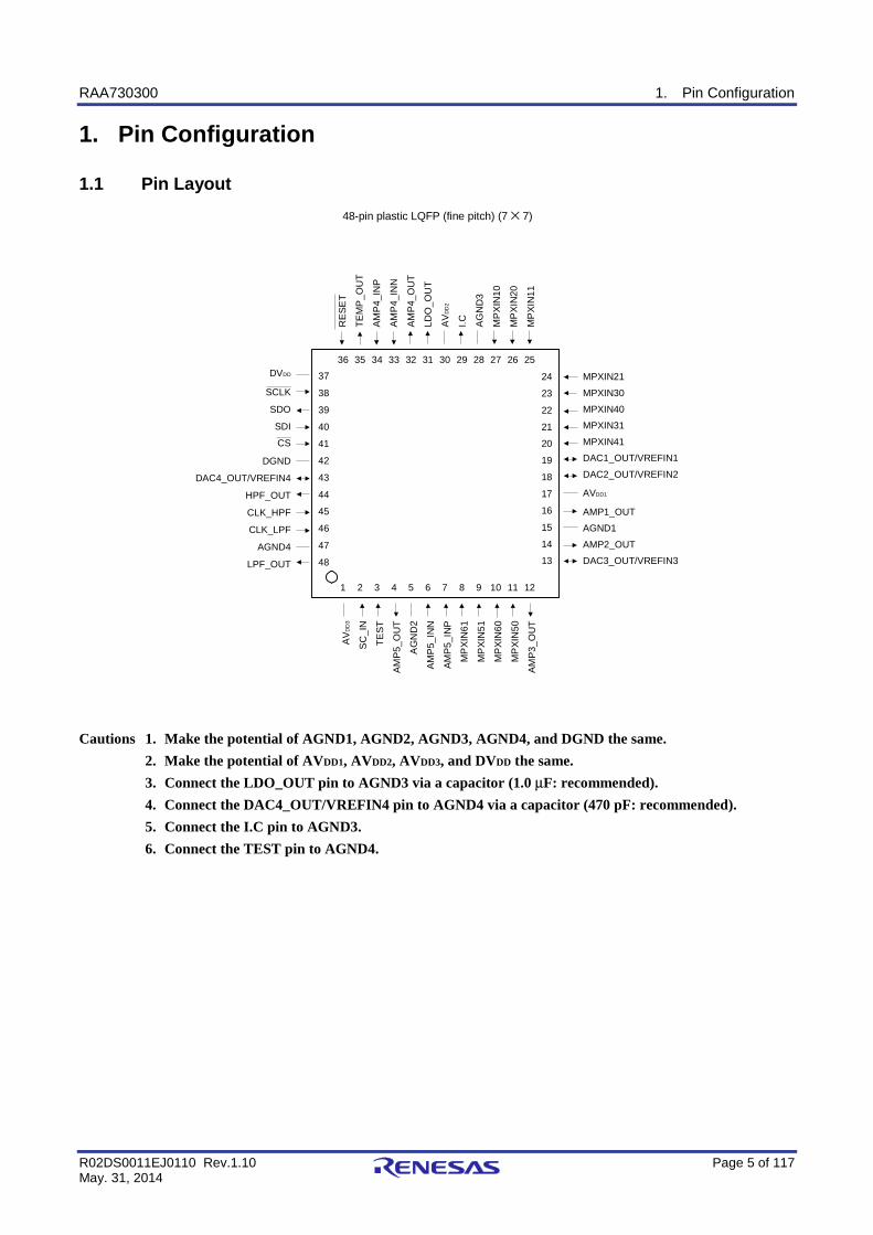
RAA730300 1. Pin Configuration
R02DS0011EJ0110 Rev.1.10 Page 5 of 117 May. 31, 2014
1. Pin Configuration
1.1 Pin Layout
48-pin plastic LQFP (fine pitch) (7 × 7)
36 35 34 33 32 31 30 29 28 27 26 25
24
23
22
21
20
19
18
17
16
15
14
13
1 2 3 4 5 6 7 8 9 10 11 12
45
41
42
43
44
37
48
46
47
40
38
39
RE
SET
AM
P4_
OU
T
LDO
_OU
T
I.C MP
XIN
10
MP
XIN
20
MP
XIN
11
AV
DD
2
AG
ND
3
AM
P4_
INN
AM
P4_
INP
TEM
P_O
UT
CS
CLK_HPF
HPF_OUT
DVDD
SCLK
SDI
LPF_OUT
CLK_LPF
DGND
DAC4_OUT/VREFIN4
AGND4
SDO MPXIN40
MPXIN21
MPXIN30
MPXIN31
MPXIN41
DAC1_OUT/VREFIN1
DAC2_OUT/VREFIN2
AVDD1
AMP1_OUT
AGND1
AMP2_OUT
DAC3_OUT/VREFIN3
AVD
D3
SC
_IN
TEST
AM
P5_
OU
T
AG
ND
2
AMP
5_IN
N
AMP
5_IN
P
MP
XIN
61
MP
XIN
51
MP
XIN
60
MP
XIN
50
AM
P3_
OU
T
Cautions 1. Make the potential of AGND1, AGND2, AGND3, AGND4, and DGND the same. 2. Make the potential of AVDD1, AVDD2, AVDD3, and DVDD the same. 3. Connect the LDO_OUT pin to AGND3 via a capacitor (1.0 μF: recommended). 4. Connect the DAC4_OUT/VREFIN4 pin to AGND4 via a capacitor (470 pF: recommended). 5. Connect the I.C pin to AGND3. 6. Connect the TEST pin to AGND4.
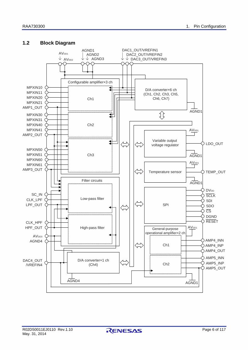
RAA730300 1. Pin Configuration
R02DS0011EJ0110 Rev.1.10 Page 6 of 117 May. 31, 2014
1.2 Block Diagram
DAC3_OUT/VREFIN3
TEMP_OUT
LDO_OUT
RESETDGND
SCLKSDISDOCS
AGND1AGND2
Ch1
Ch2
Ch3
Low-pass filter
Filter circuits
AGND3
AGND1
SPI
Variable output voltage regulator
AMP4_INNAMP4_INP
AMP5_INNAMP5_INPAMP5_OUT
AGND1
AMP4_OUT
DAC4_OUT/VREFIN4
AGND4 AGND1
AGND4
DAC1_OUT/VREFIN1DAC2_OUT/VREFIN2
MPXIN10MPXIN11MPXIN20MPXIN21
AMP1_OUT
MPXIN30MPXIN31MPXIN40MPXIN41
AMP2_OUT
MPXIN50MPXIN51MPXIN60MPXIN61
AMP3_OUT
LPF_OUTCLK_LPF
HPF_OUTCLK_HPF
SC_IN
Ch1
Ch2
AGND1
Temperature sensor
High-pass filter
AVDD3
D/A converter×1 ch(Ch4)
Configurable amplifier×3 ch
AVDD1
AVDD2
D/A converter×6 ch(Ch1, Ch2, Ch3, Ch5,
Ch6, Ch7)
AVDD1
AVDD1
DVDD
General-purposeoperational amplifier×2 ch
AVDD1
RAA730300 1. Pin Configuration
R02DS0011EJ0110 Rev.1.10 Page 7 of 117 May. 31, 2014
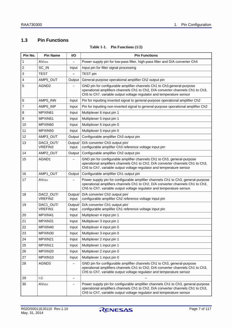
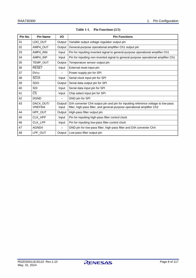
1.3 Pin Functions Table 1-1. Pin Functions (1/2)
Pin No. Pin Name I/O Pin Functions
1 AVDD3 – Power supply pin for low-pass filter, high-pass filter and D/A converter Ch4
2 SC_IN Input Input pin for filter signal processing
3 TEST – TEST pin
4 AMP5_OUT Output General-purpose operational amplifier Ch2 output pin
5 AGND2 – GND pin for configurable amplifier channels Ch1 to Ch3,general-purpose operational amplifiers channels Ch1 to Ch2, D/A converter channels Ch1 to Ch3, Ch5 to Ch7, variable output voltage regulator and temperature sensor
6 AMP5_INN Input Pin for inputting inverted signal to general-purpose operational amplifier Ch2
7 AMP5_INP Input Pin for inputting non-inverted signal to general-purpose operational amplifier Ch2
8 MPXIN61 Input Multiplexer 6 input pin 1
9 MPXIN51 Input Multiplexer 5 input pin 1
10 MPXIN60 Input Multiplexer 6 input pin 0
11 MPXIN50 Input Multiplexer 5 input pin 0
12 AMP3_OUT Output Configurable amplifier Ch3 output pin
13 DAC3_OUT/ VREFIN3
Output/ input
D/A converter Ch3 output pin/ configurable amplifier Ch3 reference voltage input pin
14 AMP2_OUT Output Configurable amplifier Ch2 output pin
15 AGND1 – GND pin for configurable amplifier channels Ch1 to Ch3, general-purpose operational amplifiers channels Ch1 to Ch2, D/A converter channels Ch1 to Ch3, Ch5 to Ch7, variable output voltage regulator and temperature sensor
16 AMP1_OUT Output Configurable amplifier Ch1 output pin
17 AVDD1 – Power supply pin for configurable amplifier channels Ch1 to Ch3, general-purpose operational amplifiers channels Ch1 to Ch2, D/A converter channels Ch1 to Ch3, Ch5 to Ch7, variable output voltage regulator and temperature sensor.
18 DAC2_OUT/ VREFIN2
Output/ input
D/A converter Ch2 output pin/ configurable amplifier Ch2 reference voltage input pin
19 DAC1_OUT/ VREFIN1
Output/ input
D/A converter Ch1 output pin/ configurable amplifier Ch1 reference voltage input pin
20 MPXIN41 Input Multiplexer 4 input pin 1
21 MPXIN31 Input Multiplexer 3 input pin 1
22 MPXIN40 Input Multiplexer 4 input pin 0
23 MPXIN30 Input Multiplexer 3 input pin 0
24 MPXIN21 Input Multiplexer 2 input pin 1
25 MPXIN11 Input Multiplexer 1 input pin 1
26 MPXIN20 Input Multiplexer 2 input pin 0
27 MPXIN10 Input Multiplexer 1 input pin 0
28 AGND3 – GND pin for configurable amplifier channels Ch1 to Ch3, general-purpose operational amplifiers channels Ch1 to Ch2, D/A converter channels Ch1 to Ch3, Ch5 to Ch7, variable output voltage regulator and temperature sensor
29 I.C – –
30 AVDD2 – Power supply pin for configurable amplifier channels Ch1 to Ch3, general-purpose operational amplifiers channels Ch1 to Ch2, D/A converter channels Ch1 to Ch3, Ch5 to Ch7, variable output voltage regulator and temperature sensor
RAA730300 1. Pin Configuration
R02DS0011EJ0110 Rev.1.10 Page 8 of 117 May. 31, 2014
Table 1-1. Pin Functions (2/2)
Pin No. Pin Name I/O Pin Functions
31 LDO_OUT Output Variable output voltage regulator output pin
32 AMP4_OUT Output General-purpose operational amplifier Ch1 output pin
33 AMP4_INN Input Pin for inputting inverted signal to general-purpose operational amplifier Ch1
34 AMP4_INP Input Pin for inputting non-inverted signal to general-purpose operational amplifier Ch1
35 TEMP_OUT Output Temperature sensor output pin
36 RESET Input External reset input pin
37 DVDD – Power supply pin for SPI
38 SCLK Input Serial clock input pin for SPI
39 SDO Output Serial data output pin for SPI
40 SDI Input Serial data input pin for SPI
41 CS Input Chip select input pin for SPI
42 DGND – GND pin for SPI
43 DAC4_OUT/ VREFIN4
Output/ input
D/A converter Ch4 output pin and pin for inputting reference voltage to low-pass filter, high-pass filter, and general-purpose operational amplifier Ch2
44 HPF_OUT Output High-pass filter output pin
45 CLK_HPF Input Pin for inputting high-pass filter control clock
46 CLK_LPF Input Pin for inputting low-pass filter control clock
47 AGND4 – GND pin for low-pass filter, high-pass filter and D/A converter Ch4
48 LPF_OUT Output Low-pass filter output pin

RAA730300 1. Pin Configuration
R02DS0011EJ0110 Rev.1.10 Page 9 of 117 May. 31, 2014
1.4 Connection of Unused Pins
Table 1-2. Connection of Unused Pins
Pin Name I/O Recommended Connection of Unused Pins
SC_IN Input Directly connect to AGND4.
AMP5_OUT Output Leave open.
AMP5_INN Input Directly connect to AGND1.
AMP5_INP Input
MPXIN61 Input
MPXIN51 Input
MPXIN60 Input
MPXIN50 Input
AMP3_OUT Output Leave open.
DAC3_OUT/VREFIN3 Output/input
AMP2_OUT Output
AMP1_OUT Output
DAC2_OUT/VREFIN2 Output/input
DAC1_OUT/VREFIN1 Output/input
MPXIN41 Input Directly connect to AGND1.
MPXIN31 Input
MPXIN40 Input
MPXIN30 Input
MPXIN21 Input
MPXIN11 Input
MPXIN20 Input
MPXIN10 Input
AMP4_OUT Output Leave open.
AMP4_INN Input Directly connect to AGND1.
AMP4_INP Input
TEMP_OUT Output Leave open.
SCLK Input Connect to Ground.Note
SDO Output Leave open.
SDI Input Connect to Ground.Note
CS Input
DAC4_OUT/VREFIN4 Output/input Leave open.
HPF_OUT Output
CLK_HPF Input
CLK_LPF Input
LPF_OUT Output
LDO_OUT Output
RESET Input Connect to DVDD directly or via a resistor. Note Ground means the same electrical potential as AGND1, AGND2, AGND3, AGND4 and DGND.
RAA730300 1. Pin Configuration
R02DS0011EJ0110 Rev.1.10 Page 10 of 117 May. 31, 2014
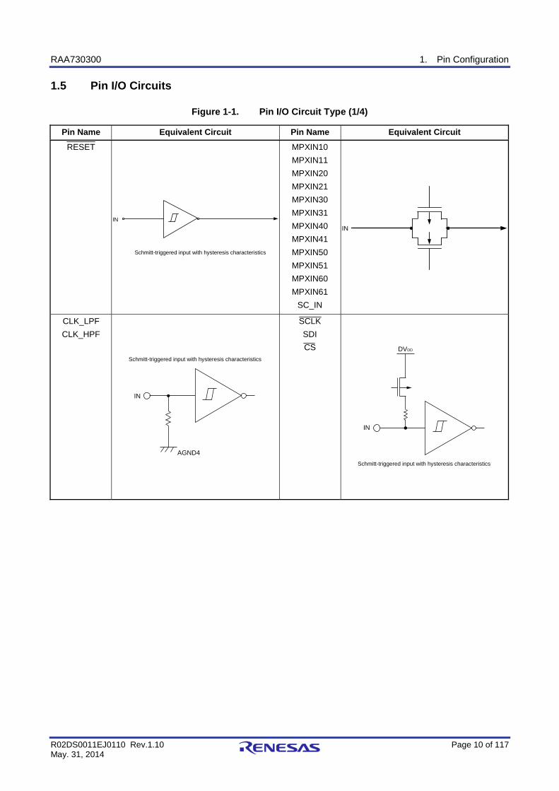
1.5 Pin I/O Circuits
Figure 1-1. Pin I/O Circuit Type (1/4)
Pin Name Equivalent Circuit Pin Name Equivalent Circuit
RESET
IN
Schmitt-triggered input with hysteresis characteristics
MPXIN10 MPXIN11 MPXIN20 MPXIN21 MPXIN30 MPXIN31 MPXIN40 MPXIN41 MPXIN50 MPXIN51 MPXIN60 MPXIN61
SC_IN
IN
CLK_LPF CLK_HPF
Schmitt-triggered input with hysteresis characteristics
IN
AGND4
SCLK SDI CS
IN
DVDD
Schmitt-triggered input with hysteresis characteristics
RAA730300 1. Pin Configuration
R02DS0011EJ0110 Rev.1.10 Page 11 of 117 May. 31, 2014
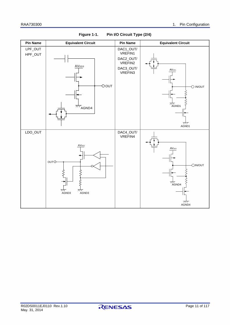
Figure 1-1. Pin I/O Circuit Type (2/4)
Pin Name Equivalent Circuit Pin Name Equivalent Circuit
LPF_OUT HPF_OUT
AVDD3
AGND4
OUT
DAC1_OUT/VREFIN1
DAC2_OUT/VREFIN2
DAC3_OUT/VREFIN3
AGND1
AGND1
AVDD1
IN/OUT
LDO_OUT
AVDD2
OUT
AGND3AGND3
DAC4_OUT/VREFIN4
AGND4
AGND4
AVDD3
IN/OUT
RAA730300 1. Pin Configuration
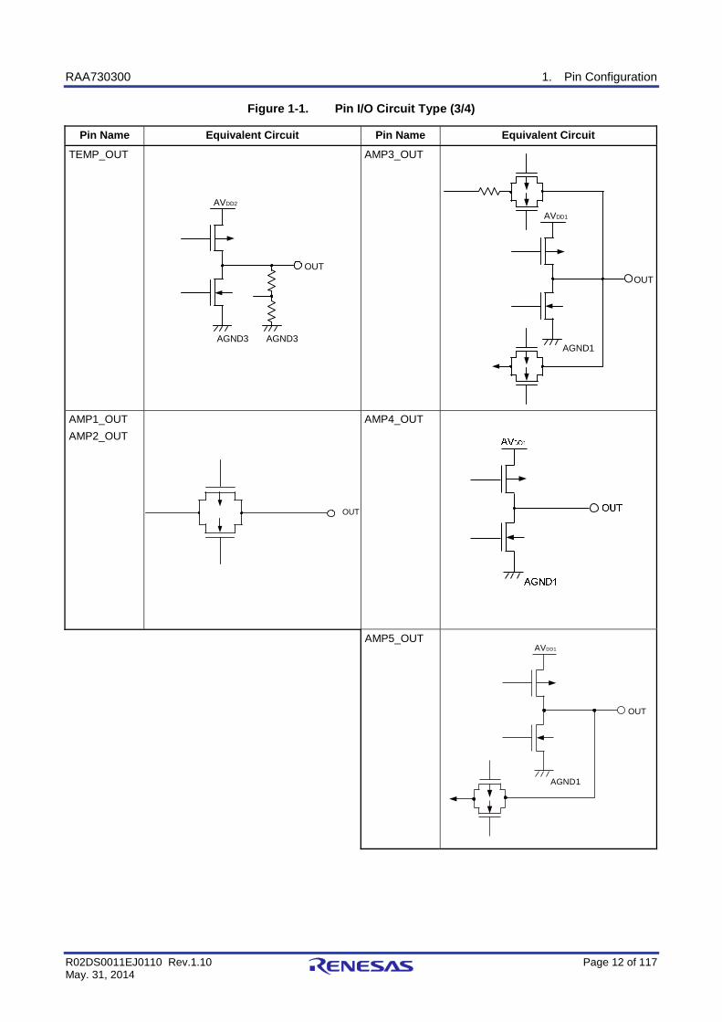
R02DS0011EJ0110 Rev.1.10 Page 12 of 117 May. 31, 2014
Figure 1-1. Pin I/O Circuit Type (3/4)
Pin Name Equivalent Circuit Pin Name Equivalent Circuit
TEMP_OUT
AVDD2
AGND3
OUT
AGND3
AMP3_OUT
AVDD1
AGND1
OUT
AMP1_OUT AMP2_OUT
OUT
AMP4_OUT
AMP5_OUT
OUT
AVDD1
AGND1
RAA730300 1. Pin Configuration
R02DS0011EJ0110 Rev.1.10 Page 13 of 117 May. 31, 2014
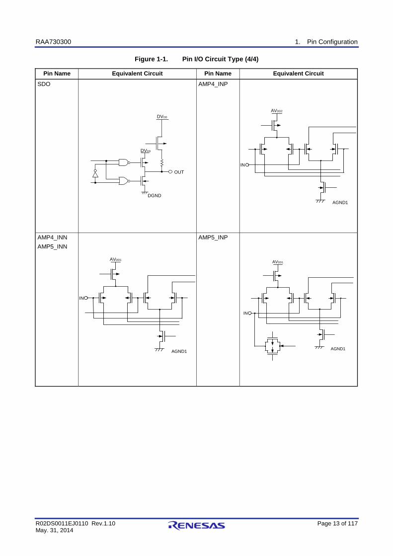
Figure 1-1. Pin I/O Circuit Type (4/4)
Pin Name Equivalent Circuit Pin Name Equivalent Circuit
SDO
DVDD
DVDD
OUT
DGND
AMP4_INP
AVDD2
AGND1
IN
AMP4_INN AMP5_INN
AVDD1
AGND1
IN
AMP5_INP
AVDD1
AGND1
IN
RAA730300 2. Configurable Amplifiers
R02DS0011EJ0110 Rev.1.10 Page 14 of 117 May. 31, 2014
2. Configurable Amplifiers
The RAA730300 has three on-chip configurable amplifier channels.
2.1 Overview of Configurable Amplifier Features
By specifying settings in the SPI control registers, the configurable amplifiers can be used to realize the following features:
• Single-channel operation
⎯ Non-inverting amplifier
• The gain can be specified between 9.5 dB and 40.1 dB in 18 steps • Four operating modes are available • Includes an input mode switching function • Includes a power-off function
⎯ Inverting amplifier
• The gain can be specified between 6 dB and 40 dB in 18 steps • Four operating modes are available • Includes an input mode switching function • Includes a power-off function
⎯ Differential amplifier
• The gain can be specified between 6 dB and 40 dB in 18 steps • Four operating modes are available • Includes an input mode switching function • Includes a power-off function
⎯ Transimpedance amplifier
• The feedback resistance can be specified between 20 kΩ and 640 kΩ in 6 steps • Four operating modes are available • Includes an input mode switching function • Includes a power-off function
⎯ General-purpose operational amplifier
• Four operating modes are available • Includes an input mode switching function • Includes a power-off function
• Multiple-channel operation
⎯ Instrumentation amplifier
• The gain can be specified between 15.5 dB and 33.5 dB in 10 steps • Four operating modes are available • Includes an input mode switching function • Includes a power-off function
And also, the output signal from D/A converter Ch n (n = 1 to 3, 5 to 7) can be used as the reference voltage for each configurable amplifier. If D/A converters are powered off, the external reference voltage is to be input to DACn_OUT/VREFINn (n = 1 to 3) pin. For details about use of D/A converter, see 4. D/A Converter.
<R>
RAA730300 2. Configurable Amplifiers
R02DS0011EJ0110 Rev.1.10 Page 15 of 117 May. 31, 2014
2.2 Block Diagram
Figure 2-1. Block Diagram of Configurable Amplifier Ch1
SW12SW11 SW13SW10 AMPG11AMPG13 AMPG12 AMPG10AMPG14
+
-
8-bitDAC1
MPXIN20
MPXIN21
MPXIN10
MPXIN11
MPX2
MPX1
AMP1_OUT
SW11
SW12
SW13
MPX20 MPX31 MPX30MPX10 MPX21MPX11
CC10CC11
AMP1OF DAC1OF DAC12 DAC11DAC14 DAC13 01CAD51CAD61CADDAC17
MPX3
MPXIN30
MPXIN31
SW00 SW01
SW00
SW01
AVDD1
AGND1
VRB0VRT0 VRB1VRT1
DAC5
DAC5OF
DAC52 DAC51DAC54 DAC53 05CAD55CAD65CADDAC57
SW10
IMS1
DAC1_OUT/VREFIN1
D/A converterCh6 output signal
MPX setting register 1 (MPX1) Power control register 1 (PC1)
Power control register 2 (PC2)
DAC control register 1 (DAC1C) DAC reference voltage control register (DACRC)
Internal bus
Internal busInput mode control register (IMS)
Configuration register 2(CONFIG2)
Configuration register 1(CONFIG1)
Gain control register 1 (GC1)
AMP operation mode control register (AOMC)
DAC control register 5 (DAC5C)
8-bit
Source of configurable ampCh2 non-inverted input
Selector
Selector
Selector
MPX5, MPX6, MPX7
RAA730300 2. Configurable Amplifiers
R02DS0011EJ0110 Rev.1.10 Page 16 of 117 May. 31, 2014
Figure 2-2. Block Diagram of Configurable Amplifier Ch2
SW22SW21 SW23SW20 AMPG21AMPG23 AMPG22 AMPG20AMPG24
+
–
DAC2
SW23
MPX30 MPX41 MPX40MPX10 MPX31MPX11
CC20CC21
AMP2OF DAC2OF DAC22 DAC21DAC24 DAC23 02CAD52CAD62CADDAC27
SW00 SW02
VRB0VRT0 VRB1VRT1
DAC6
DAC6OF
DAC62 DAC61DAC64 DAC63 06CAD56CAD66CADDAC67I MS2
AVDD1
MPXIN10
MPXIN11
MPX1
MPXIN40
MPXIN41
MPXIN30
MPXIN31
MPX3
MPX4
SW00
SW20SW02
AGND1
AMP2_OUT
DAC2_OUT/VREFIN2
SW22
SW21
8-bit
D/A converterCh5 output signal
MPX setting register 1 (MPX1) Power control register 1 (PC1)
Power control register 2 (PC2)
DAC control register 2 (DAC2C) DAC reference voltage control register (DACRC)
Internal busInput mode control register (IMS)
Configuration register 2(CONFIG2)
Configuration register 1(CONFIG1)
Gain control register 2 (GC2)
AMP operation mode control register (AOMC)
DAC control register 6 (DAC6C)
8-bit
Source of configurable ampCh1 non-inverted input
Selector
Selector
Selector
Internal bus
MPX5, MPX6, MPX7
<R>
RAA730300 2. Configurable Amplifiers
R02DS0011EJ0110 Rev.1.10 Page 17 of 117 May. 31, 2014
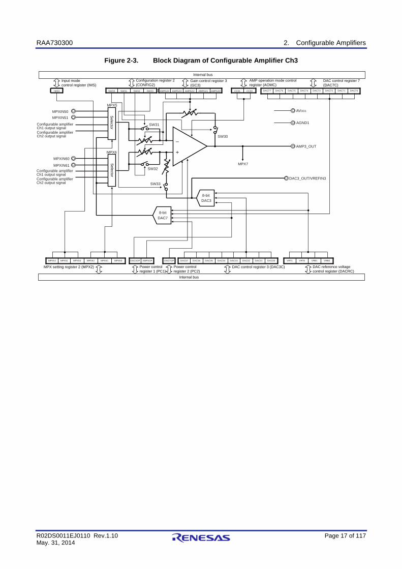
Figure 2-3. Block Diagram of Configurable Amplifier Ch3
SW32SW31 SW33SW30 AMPG31AMPG33 AMPG32 AMPG30AMPG34
+
–
CC30CC31
AMP3OF DAC3OF DAC32 DAC31DAC34 DAC33 03CAD53CAD63CADDAC37 VRB0VRT0 VRB1VRT1DAC7OF
DAC72 DAC71DAC74 DAC73 07CAD57CAD67CADDAC77I MS3
MPX62 MPX61 MPX60MPX51 MPX50MPX52
MPXIN50MPXIN51
MPX6
MPXIN60
MPXIN61
SW30
SW31
MPX5
SW32
SW33
DAC7
MPX7
DAC3
AMP3_OUT
DAC3_OUT/VREFIN3
AVDD1
AGND1
8-bit
Configurable amplifierCh1 output signal
MPX setting register 2 (MPX2) Power control register 1 (PC1)
Power control register 2 (PC2)
DAC control register 3 (DAC3C) DAC reference voltage control register (DACRC)
Internal busInput mode control register (IMS)
Configuration register 2(CONFIG2)
Gain control register 3 (GC3)
AMP operation mode control register (AOMC)
DAC control register 7 (DAC7C)
8-bit
Selector
Selector
Internal bus
Configurable amplifierCh2 output signal
Configurable amplifierCh1 output signalConfigurable amplifierCh2 output signal
RAA730300 2. Configurable Amplifiers
R02DS0011EJ0110 Rev.1.10 Page 18 of 117 May. 31, 2014
2.3 Registers Controlling the Configurable Amplifiers
The configurable amplifiers are controlled by the following 10 registers:
• Configuration register 1 (CONFIG1)
• Configuration register 2 (CONFIG2)
• MPX setting register 1 (MPX1)
• MPX setting register 2 (MPX2)
• Gain control register 1 (GC1)
• Gain control register 2 (GC2)
• Gain control register 3 (GC3)
• AMP operation mode control register (AOMC)
• Power control register 1 (PC1) • Input mode control register (IMS)
RAA730300 2. Configurable Amplifiers
R02DS0011EJ0110 Rev.1.10 Page 19 of 117 May. 31, 2014
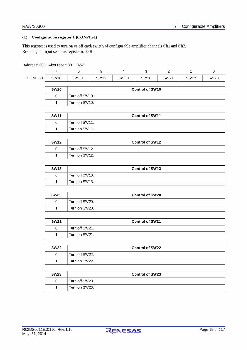
(1) Configuration register 1 (CONFIG1)
This register is used to turn on or off each switch of configurable amplifier channels Ch1 and Ch2. Reset signal input sets this register to 88H.
Address: 00H After reset: 88H R/W
7 6 5 4 3 2 1 0
CONFIG1 SW10 SW11 SW12 SW13 SW20 SW21 SW22 SW23
SW10 Control of SW10
0 Turn off SW10.
1 Turn on SW10.
SW11 Control of SW11
0 Turn off SW11.
1 Turn on SW11.
SW12 Control of SW12
0 Turn off SW12.
1 Turn on SW12.
SW13 Control of SW13
0 Turn off SW13.
1 Turn on SW13.
SW20 Control of SW20
0 Turn off SW20.
1 Turn on SW20.
SW21 Control of SW21
0 Turn off SW21.
1 Turn on SW21.
SW22 Control of SW22
0 Turn off SW22.
1 Turn on SW22.
SW23 Control of SW23
0 Turn off SW23.
1 Turn on SW23.

RAA730300 2. Configurable Amplifiers
R02DS0011EJ0110 Rev.1.10 Page 20 of 117 May. 31, 2014
(2) Configuration register 2 (CONFIG2)
This register is used to turn on or off each switch of configurable amplifier channels Ch1 to Ch3. Reset signal input sets this register to 80H.
Address: 01H After reset: 80H R/W
7 6 5 4 3 2 1 0
CONFIG2 SW30 SW31 SW32 SW33 0 SW02 SW01 SW00
SW30 Control of SW30
0 Turn off SW30.
1 Turn on SW30.
SW31 Control of SW31
0 Turn off SW31.
1 Turn on SW31.
SW32 Control of SW32
0 Turn off SW32.
1 Turn on SW32.
SW33 Control of SW33
0 Turn off SW33.
1 Turn on SW33.
SW02 Control of SW02
0 Turn off SW02.
1 Turn on SW02.
SW01 Control of SW01
0 Turn off SW01.
1 Turn on SW01.
SW00 Control of SW00
0 Turn off SW00.
1 Turn on SW00. Remark Bit 3 can be set to 1, but this has no effect on the function.
RAA730300 2. Configurable Amplifiers
R02DS0011EJ0110 Rev.1.10 Page 21 of 117 May. 31, 2014
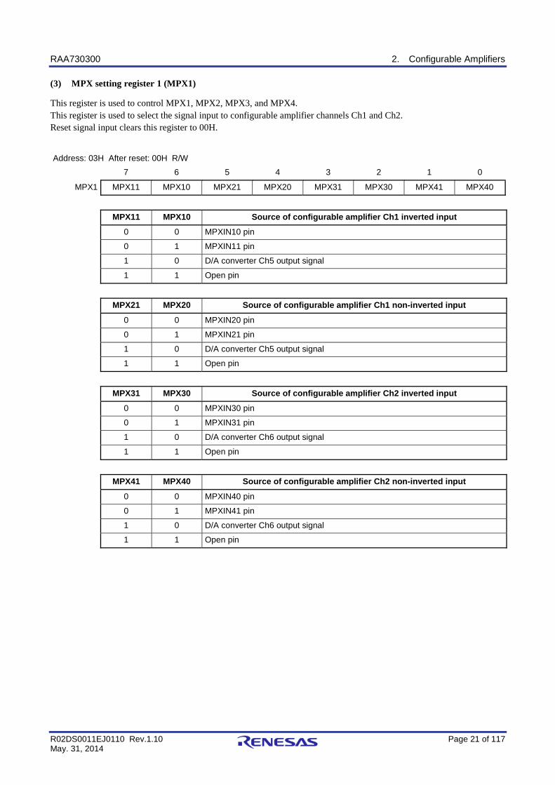
(3) MPX setting register 1 (MPX1)
This register is used to control MPX1, MPX2, MPX3, and MPX4. This register is used to select the signal input to configurable amplifier channels Ch1 and Ch2. Reset signal input clears this register to 00H.
Address: 03H After reset: 00H R/W
7 6 5 4 3 2 1 0
MPX1 MPX11 MPX10 MPX21 MPX20 MPX31 MPX30 MPX41 MPX40
MPX11 MPX10 Source of configurable amplifier Ch1 inverted input
0 0 MPXIN10 pin
0 1 MPXIN11 pin
1 0 D/A converter Ch5 output signal
1 1 Open pin
MPX21 MPX20 Source of configurable amplifier Ch1 non-inverted input
0 0 MPXIN20 pin
0 1 MPXIN21 pin
1 0 D/A converter Ch5 output signal
1 1 Open pin
MPX31 MPX30 Source of configurable amplifier Ch2 inverted input
0 0 MPXIN30 pin
0 1 MPXIN31 pin
1 0 D/A converter Ch6 output signal
1 1 Open pin
MPX41 MPX40 Source of configurable amplifier Ch2 non-inverted input
0 0 MPXIN40 pin
0 1 MPXIN41 pin
1 0 D/A converter Ch6 output signal
1 1 Open pin

RAA730300 2. Configurable Amplifiers
R02DS0011EJ0110 Rev.1.10 Page 22 of 117 May. 31, 2014
(4) MPX setting register 2 (MPX2)
This register is used to control MPX5 and MPX6. This register is used to select the signal input to configurable amplifier Ch3. Reset signal input clears this register to 00H.
Address: 04H After reset: 00H R/W
7 6 5 4 3 2 1 0
MPX2 0 MPX52 MPX51 MPX50 0 MPX62 MPX61 MPX60
MPX52 MPX51 MPX50 Source of configurable amplifier Ch3 inverted input
0 0 0 MPXIN50 pin
0 0 1 MPXIN51 pin
0 1 0 Configurable amplifier Ch1 output signal
0 1 1 Configurable amplifier Ch2 output signal
1 0 0 D/A converter Ch7 output signal
Other than above Setting prohibited
MPX62 MPX61 MPX60 Source of configurable amplifier Ch3 non-inverted input
0 0 0 MPXIN60 pin
0 0 1 MPXIN61 pin
0 1 0 Output signal of configurable amplifier Ch1
0 1 1 Configurable amplifier Ch2 output signal
1 0 0 D/A converter Ch7 output signal
Other than above Setting prohibited Remark Bits 7 and 3 can be set to 1, but this has no effect on the function.
RAA730300 2. Configurable Amplifiers
R02DS0011EJ0110 Rev.1.10 Page 23 of 117 May. 31, 2014
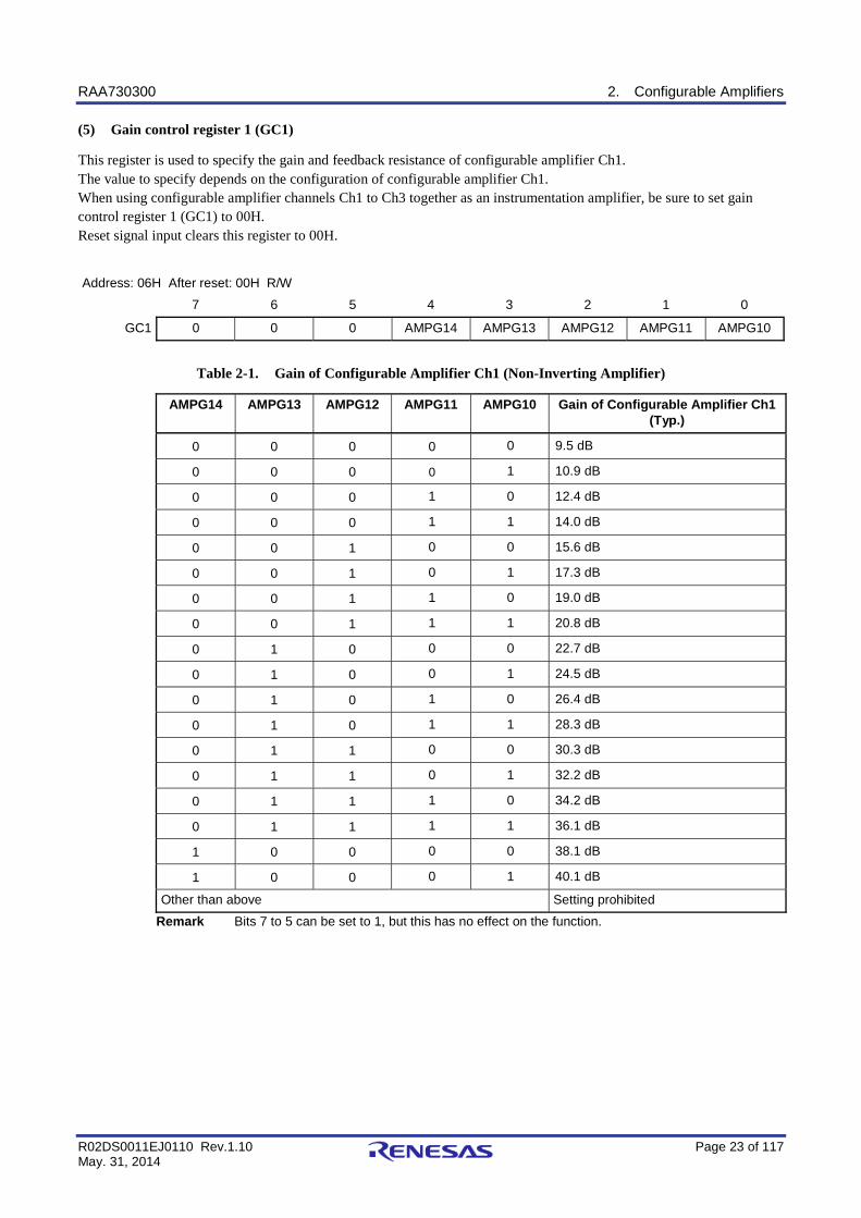
(5) Gain control register 1 (GC1)
This register is used to specify the gain and feedback resistance of configurable amplifier Ch1. The value to specify depends on the configuration of configurable amplifier Ch1. When using configurable amplifier channels Ch1 to Ch3 together as an instrumentation amplifier, be sure to set gain control register 1 (GC1) to 00H. Reset signal input clears this register to 00H.
Address: 06H After reset: 00H R/W
7 6 5 4 3 2 1 0
GC1 0 0 0 AMPG14 AMPG13 AMPG12 AMPG11 AMPG10
Table 2-1. Gain of Configurable Amplifier Ch1 (Non-Inverting Amplifier)
AMPG14 AMPG13 AMPG12 AMPG11 AMPG10 Gain of Configurable Amplifier Ch1 (Typ.)
0 0 0 0 0 9.5 dB
0 0 0 0 1 10.9 dB
0 0 0 1 0 12.4 dB
0 0 0 1 1 14.0 dB
0 0 1 0 0 15.6 dB
0 0 1 0 1 17.3 dB
0 0 1 1 0 19.0 dB
0 0 1 1 1 20.8 dB
0 1 0 0 0 22.7 dB
0 1 0 0 1 24.5 dB
0 1 0 1 0 26.4 dB
0 1 0 1 1 28.3 dB
0 1 1 0 0 30.3 dB
0 1 1 0 1 32.2 dB
0 1 1 1 0 34.2 dB
0 1 1 1 1 36.1 dB
1 0 0 0 0 38.1 dB
1 0 0 0 1 40.1 dB
Other than above Setting prohibited
Remark Bits 7 to 5 can be set to 1, but this has no effect on the function.
RAA730300 2. Configurable Amplifiers
R02DS0011EJ0110 Rev.1.10 Page 24 of 117 May. 31, 2014
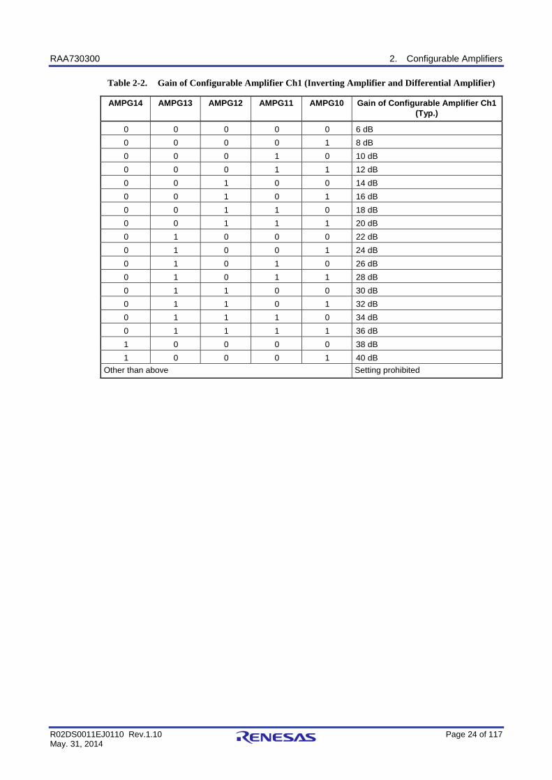
Table 2-2. Gain of Configurable Amplifier Ch1 (Inverting Amplifier and Differential Amplifier)
AMPG14 AMPG13 AMPG12 AMPG11 AMPG10 Gain of Configurable Amplifier Ch1 (Typ.)
0 0 0 0 0 6 dB 0 0 0 0 1 8 dB 0 0 0 1 0 10 dB 0 0 0 1 1 12 dB 0 0 1 0 0 14 dB 0 0 1 0 1 16 dB 0 0 1 1 0 18 dB 0 0 1 1 1 20 dB 0 1 0 0 0 22 dB 0 1 0 0 1 24 dB 0 1 0 1 0 26 dB 0 1 0 1 1 28 dB 0 1 1 0 0 30 dB 0 1 1 0 1 32 dB 0 1 1 1 0 34 dB 0 1 1 1 1 36 dB 1 0 0 0 0 38 dB 1 0 0 0 1 40 dB
Other than above Setting prohibited

RAA730300 2. Configurable Amplifiers
R02DS0011EJ0110 Rev.1.10 Page 25 of 117 May. 31, 2014
Table 2-3. Feedback Resistance of Configurable Amplifier Ch1 (Transimpedance Amplifier)
AMPG14 AMPG13 AMPG12 AMPG11 AMPG10 Feedback Resistance of Configurable Amplifier Ch1 (Typ.)
0 0 0 0 0 20 kΩ 0 0 0 0 1 0 0 0 1 0 0 0 0 1 1 40 kΩ 0 0 1 0 0 0 0 1 0 1 0 0 1 1 0 80 kΩ 0 0 1 1 1 0 1 0 0 0 0 1 0 0 1 160 kΩ 0 1 0 1 0 0 1 0 1 1 0 1 1 0 0 320 kΩ 0 1 1 0 1 0 1 1 1 0 0 1 1 1 1 640 kΩ 1 0 0 0 0 1 0 0 0 1
Other than above Setting prohibited
RAA730300 2. Configurable Amplifiers
R02DS0011EJ0110 Rev.1.10 Page 26 of 117 May. 31, 2014
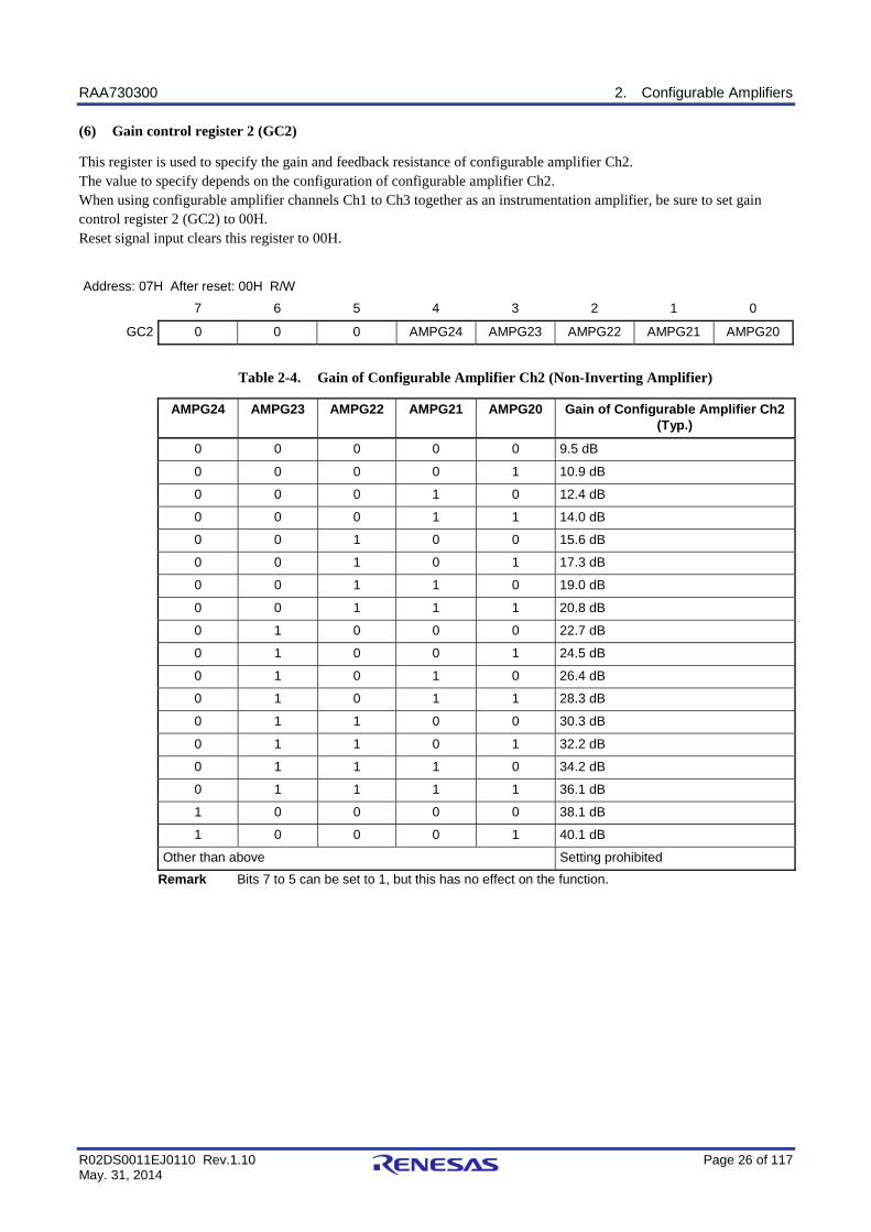
(6) Gain control register 2 (GC2)
This register is used to specify the gain and feedback resistance of configurable amplifier Ch2. The value to specify depends on the configuration of configurable amplifier Ch2. When using configurable amplifier channels Ch1 to Ch3 together as an instrumentation amplifier, be sure to set gain control register 2 (GC2) to 00H. Reset signal input clears this register to 00H.
Address: 07H After reset: 00H R/W
7 6 5 4 3 2 1 0
GC2 0 0 0 AMPG24 AMPG23 AMPG22 AMPG21 AMPG20
Table 2-4. Gain of Configurable Amplifier Ch2 (Non-Inverting Amplifier)
AMPG24 AMPG23 AMPG22 AMPG21 AMPG20 Gain of Configurable Amplifier Ch2 (Typ.)
0 0 0 0 0 9.5 dB
0 0 0 0 1 10.9 dB
0 0 0 1 0 12.4 dB
0 0 0 1 1 14.0 dB
0 0 1 0 0 15.6 dB
0 0 1 0 1 17.3 dB
0 0 1 1 0 19.0 dB
0 0 1 1 1 20.8 dB
0 1 0 0 0 22.7 dB
0 1 0 0 1 24.5 dB
0 1 0 1 0 26.4 dB
0 1 0 1 1 28.3 dB
0 1 1 0 0 30.3 dB
0 1 1 0 1 32.2 dB
0 1 1 1 0 34.2 dB
0 1 1 1 1 36.1 dB
1 0 0 0 0 38.1 dB
1 0 0 0 1 40.1 dB
Other than above Setting prohibited
Remark Bits 7 to 5 can be set to 1, but this has no effect on the function.

RAA730300 2. Configurable Amplifiers
R02DS0011EJ0110 Rev.1.10 Page 27 of 117 May. 31, 2014
Table 2-5. Gain of Configurable Amplifier Ch2 (Inverting Amplifier and Differential Amplifier)
AMPG24 AMPG23 AMPG22 AMPG21 AMPG20 Gain of Configurable Amplifier Ch2 (Typ.)
0 0 0 0 0 6 dB
0 0 0 0 1 8 dB
0 0 0 1 0 10 dB
0 0 0 1 1 12 dB
0 0 1 0 0 14 dB
0 0 1 0 1 16 dB
0 0 1 1 0 18 dB
0 0 1 1 1 20 dB
0 1 0 0 0 22 dB
0 1 0 0 1 24 dB
0 1 0 1 0 26 dB
0 1 0 1 1 28 dB
0 1 1 0 0 30 dB
0 1 1 0 1 32 dB
0 1 1 1 0 34 dB
0 1 1 1 1 36 dB
1 0 0 0 0 38 dB
1 0 0 0 1 40 dB
Other than above Setting prohibited

RAA730300 2. Configurable Amplifiers
R02DS0011EJ0110 Rev.1.10 Page 28 of 117 May. 31, 2014
Table 2-6. Feedback Resistance of Configurable Amplifier Ch2 (Transimpedance Amplifier)
AMPG24 AMPG23 AMPG22 AMPG21 AMPG20 Feedback Resistance of Configurable Amplifier Ch2 (Typ.)
0 0 0 0 0 20 kΩ
0 0 0 0 1
0 0 0 1 0
0 0 0 1 1 40 kΩ
0 0 1 0 0
0 0 1 0 1
0 0 1 1 0 80 kΩ
0 0 1 1 1
0 1 0 0 0
0 1 0 0 1 160 kΩ
0 1 0 1 0
0 1 0 1 1
0 1 1 0 0 320 kΩ
0 1 1 0 1
0 1 1 1 0
0 1 1 1 1 640 kΩ
1 0 0 0 0
1 0 0 0 1
Other than above Setting prohibited

RAA730300 2. Configurable Amplifiers
R02DS0011EJ0110 Rev.1.10 Page 29 of 117 May. 31, 2014
(7) Gain control register 3 (GC3)
This register is used to specify the gain and feedback resistance of configurable amplifier Ch3. The value to specify depends on the configuration of configurable amplifier Ch3. When using configurable amplifier channels Ch1 to Ch3 together as an instrumentation amplifier, be sure to set gain control register 1 (GC1) and gain control register 2 (GC2) to 00H, respectively. Reset signal input clears this register to 00H.
Address: 08H After reset: 00H R/W
7 6 5 4 3 2 1 0
GC3 0 0 0 AMPG34 AMPG33 AMPG32 AMPG31 AMPG30
Table 2-7. Gain of Configurable Amplifier Ch3 (Non-Inverting Amplifier)
AMPG34 AMPG33 AMPG32 AMPG31 AMPG30 Gain of Configurable Amplifier Ch3 (Typ.)
0 0 0 0 0 9.5 dB
0 0 0 0 1 10.9 dB
0 0 0 1 0 12.4 dB
0 0 0 1 1 14.0 dB
0 0 1 0 0 15.6 dB
0 0 1 0 1 17.3 dB
0 0 1 1 0 19.0 dB
0 0 1 1 1 20.8 dB
0 1 0 0 0 22.7 dB
0 1 0 0 1 24.5 dB
0 1 0 1 0 26.4 dB
0 1 0 1 1 28.3 dB
0 1 1 0 0 30.3 dB
0 1 1 0 1 32.2 dB
0 1 1 1 0 34.2 dB
0 1 1 1 1 36.1 dB
1 0 0 0 0 38.1 dB
1 0 0 0 1 40.1 dB
Other than above Setting prohibited
Remark Bits 7 to 5 can be set to 1, but this has no effect on the function.
RAA730300 2. Configurable Amplifiers
R02DS0011EJ0110 Rev.1.10 Page 30 of 117 May. 31, 2014
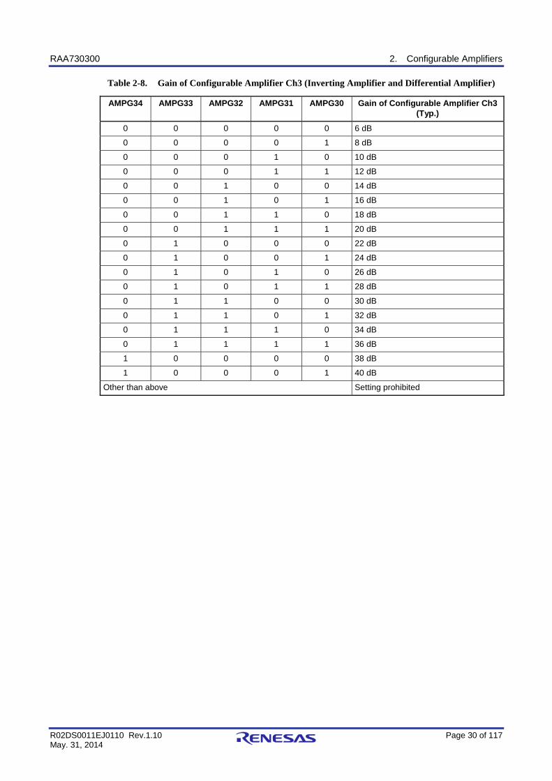
Table 2-8. Gain of Configurable Amplifier Ch3 (Inverting Amplifier and Differential Amplifier)
AMPG34 AMPG33 AMPG32 AMPG31 AMPG30 Gain of Configurable Amplifier Ch3 (Typ.)
0 0 0 0 0 6 dB
0 0 0 0 1 8 dB
0 0 0 1 0 10 dB
0 0 0 1 1 12 dB
0 0 1 0 0 14 dB
0 0 1 0 1 16 dB
0 0 1 1 0 18 dB
0 0 1 1 1 20 dB
0 1 0 0 0 22 dB
0 1 0 0 1 24 dB
0 1 0 1 0 26 dB
0 1 0 1 1 28 dB
0 1 1 0 0 30 dB
0 1 1 0 1 32 dB
0 1 1 1 0 34 dB
0 1 1 1 1 36 dB
1 0 0 0 0 38 dB
1 0 0 0 1 40 dB
Other than above Setting prohibited
RAA730300 2. Configurable Amplifiers
R02DS0011EJ0110 Rev.1.10 Page 31 of 117 May. 31, 2014
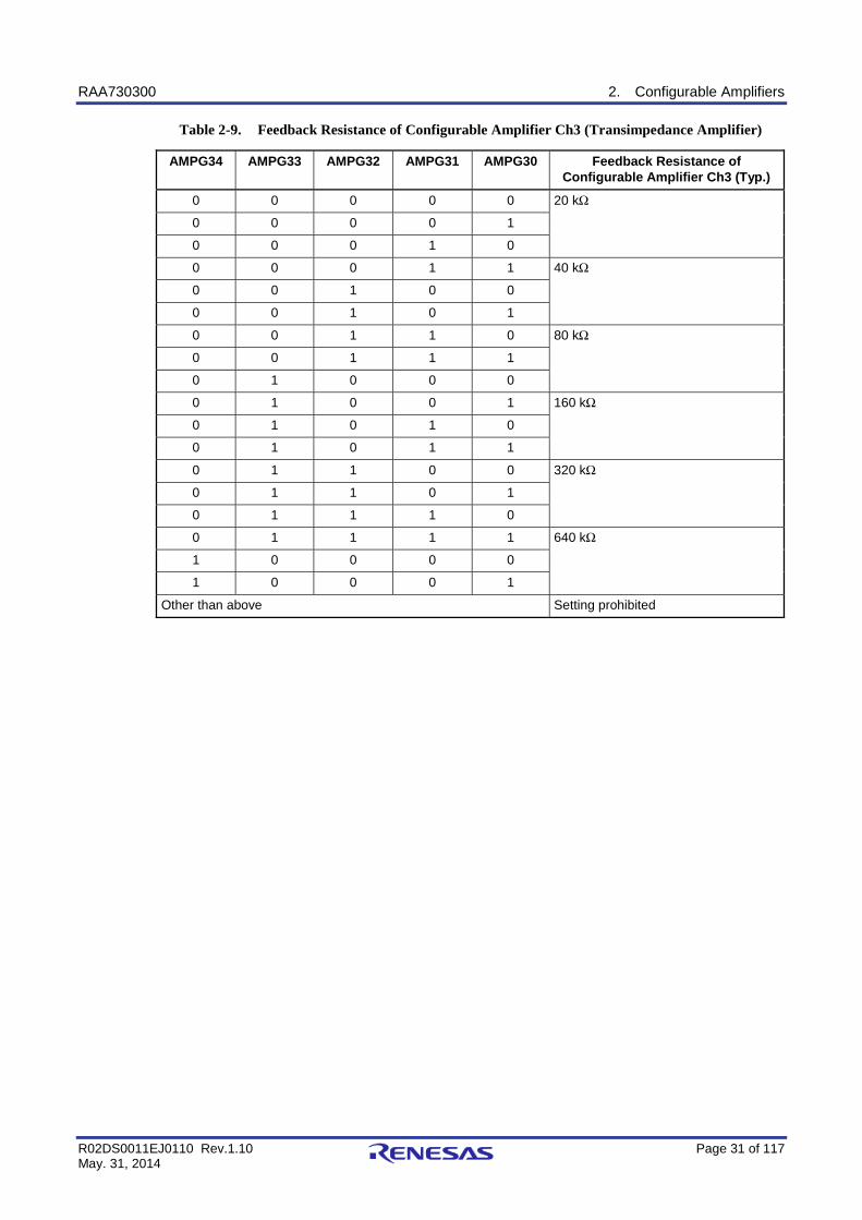
Table 2-9. Feedback Resistance of Configurable Amplifier Ch3 (Transimpedance Amplifier)
AMPG34 AMPG33 AMPG32 AMPG31 AMPG30 Feedback Resistance of Configurable Amplifier Ch3 (Typ.)
0 0 0 0 0 20 kΩ
0 0 0 0 1
0 0 0 1 0
0 0 0 1 1 40 kΩ
0 0 1 0 0
0 0 1 0 1
0 0 1 1 0 80 kΩ
0 0 1 1 1
0 1 0 0 0
0 1 0 0 1 160 kΩ
0 1 0 1 0
0 1 0 1 1
0 1 1 0 0 320 kΩ
0 1 1 0 1
0 1 1 1 0
0 1 1 1 1 640 kΩ
1 0 0 0 0
1 0 0 0 1
Other than above Setting prohibited
RAA730300 2. Configurable Amplifiers
R02DS0011EJ0110 Rev.1.10 Page 32 of 117 May. 31, 2014
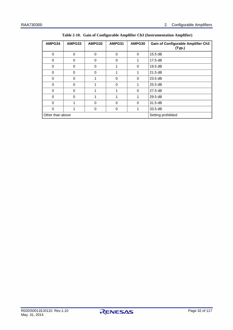
Table 2-10. Gain of Configurable Amplifier Ch3 (Instrumentation Amplifier)
AMPG34 AMPG33 AMPG32 AMPG31 AMPG30 Gain of Configurable Amplifier Ch3 (Typ.)
0 0 0 0 0 15.5 dB
0 0 0 0 1 17.5 dB
0 0 0 1 0 19.5 dB
0 0 0 1 1 21.5 dB
0 0 1 0 0 23.5 dB
0 0 1 0 1 25.5 dB
0 0 1 1 0 27.5 dB
0 0 1 1 1 29.5 dB
0 1 0 0 0 31.5 dB
0 1 0 0 1 33.5 dB
Other than above Setting prohibited
RAA730300 2. Configurable Amplifiers
R02DS0011EJ0110 Rev.1.10 Page 33 of 117 May. 31, 2014
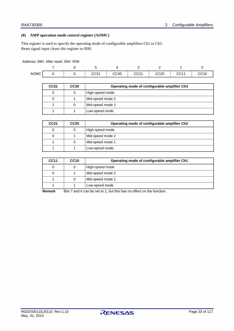
(8) AMP operation mode control register (AOMC)
This register is used to specify the operating mode of configurable amplifiers Ch1 to Ch3. Reset signal input clears this register to 00H.
Address: 09H After reset: 00H R/W
7 6 5 4 3 2 1 0
AOMC 0 0 CC31 CC30 CC21 CC20 CC11 CC10
CC31 CC30 Operating mode of configurable amplifier Ch3
0 0 High-speed mode
0 1 Mid-speed mode 2
1 0 Mid-speed mode 1
1 1 Low-speed mode
CC21 CC20 Operating mode of configurable amplifier Ch2
0 0 High-speed mode
0 1 Mid-speed mode 2
1 0 Mid-speed mode 1
1 1 Low-speed mode
CC11 CC10 Operating mode of configurable amplifier Ch1
0 0 High-speed mode
0 1 Mid-speed mode 2
1 0 Mid-speed mode 1
1 1 Low-speed mode
Remark Bits 7 and 6 can be set to 1, but this has no effect on the function.
RAA730300 2. Configurable Amplifiers
R02DS0011EJ0110 Rev.1.10 Page 34 of 117 May. 31, 2014
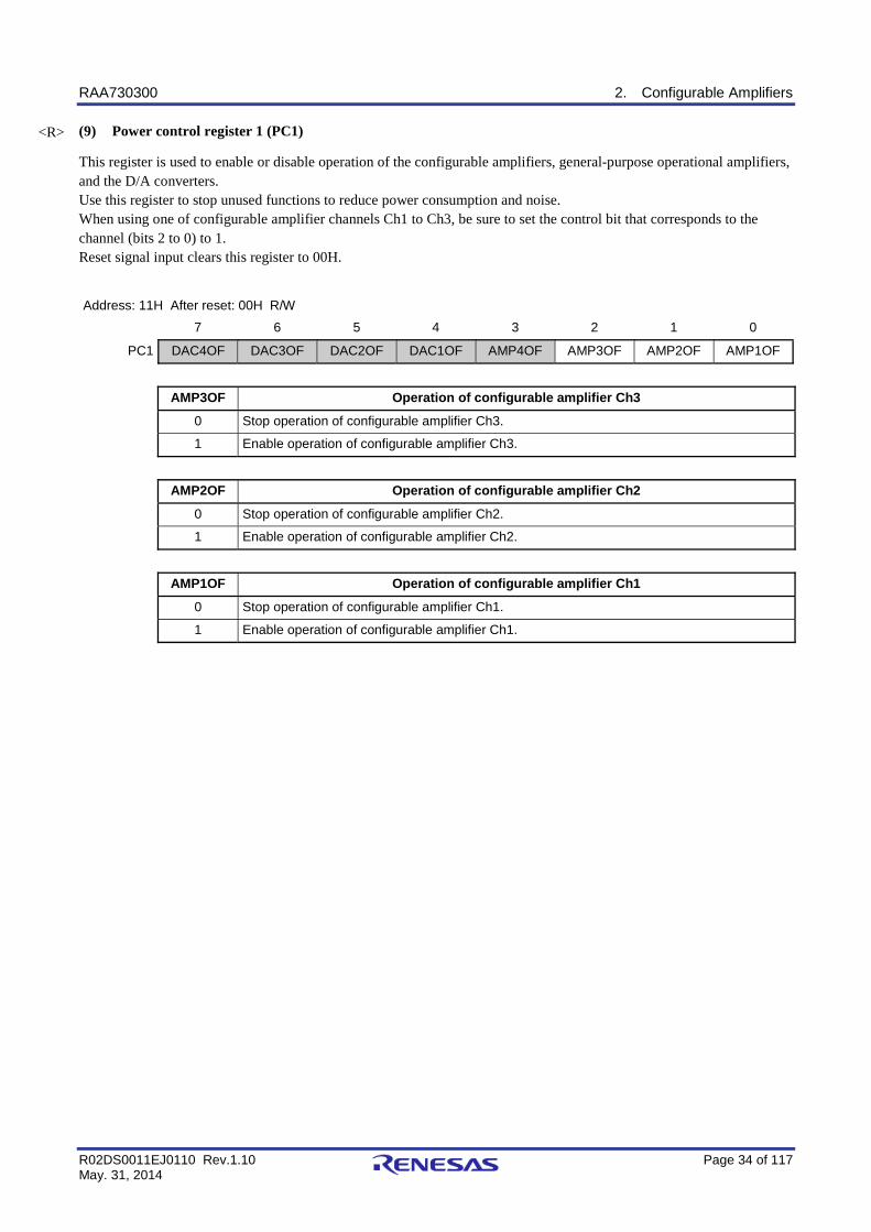
(9) Power control register 1 (PC1)
This register is used to enable or disable operation of the configurable amplifiers, general-purpose operational amplifiers, and the D/A converters. Use this register to stop unused functions to reduce power consumption and noise. When using one of configurable amplifier channels Ch1 to Ch3, be sure to set the control bit that corresponds to the channel (bits 2 to 0) to 1. Reset signal input clears this register to 00H.
Address: 11H After reset: 00H R/W
7 6 5 4 3 2 1 0
PC1 DAC4OF DAC3OF DAC2OF DAC1OF AMP4OF AMP3OF AMP2OF AMP1OF
AMP3OF Operation of configurable amplifier Ch3
0 Stop operation of configurable amplifier Ch3.
1 Enable operation of configurable amplifier Ch3.
AMP2OF Operation of configurable amplifier Ch2
0 Stop operation of configurable amplifier Ch2.
1 Enable operation of configurable amplifier Ch2.
AMP1OF Operation of configurable amplifier Ch1
0 Stop operation of configurable amplifier Ch1.
1 Enable operation of configurable amplifier Ch1.
<R>
RAA730300 2. Configurable Amplifiers
R02DS0011EJ0110 Rev.1.10 Page 35 of 117 May. 31, 2014
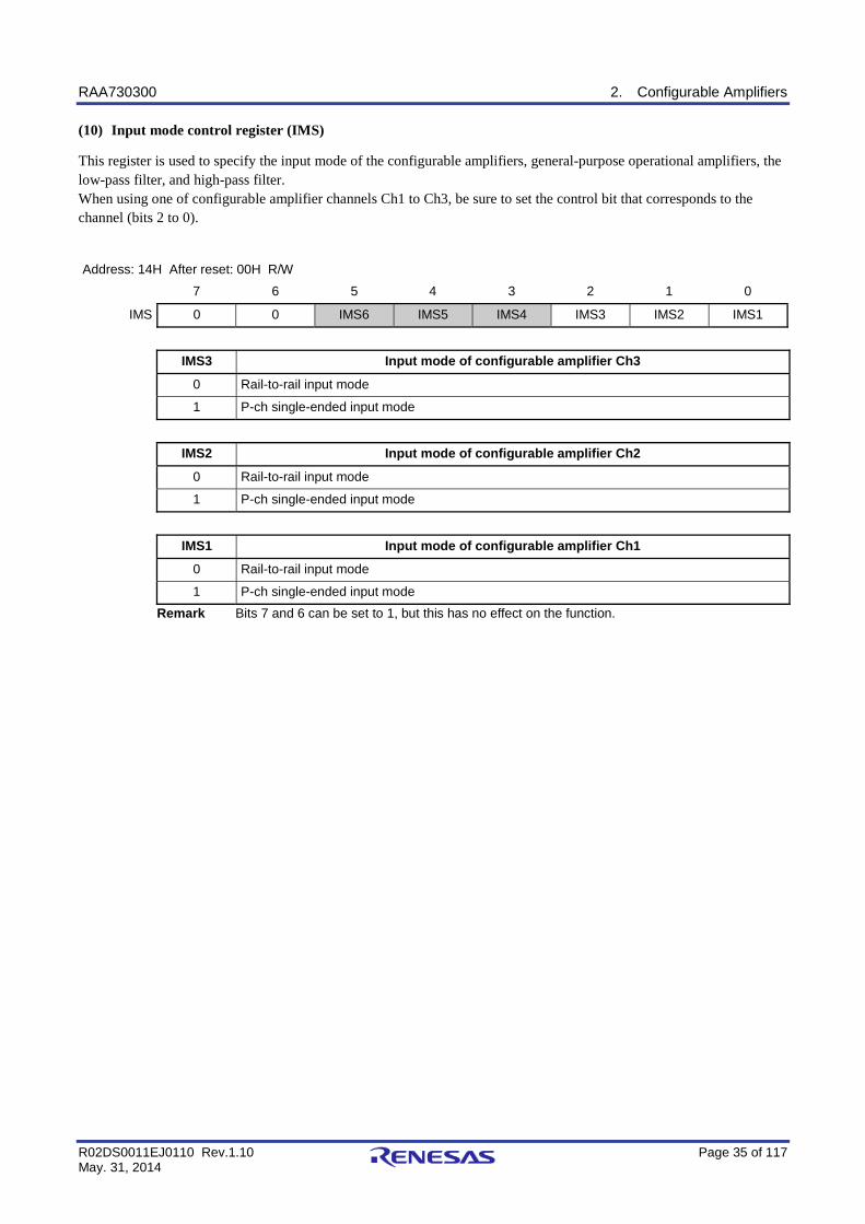
(10) Input mode control register (IMS)
This register is used to specify the input mode of the configurable amplifiers, general-purpose operational amplifiers, the low-pass filter, and high-pass filter. When using one of configurable amplifier channels Ch1 to Ch3, be sure to set the control bit that corresponds to the channel (bits 2 to 0).
Address: 14H After reset: 00H R/W
7 6 5 4 3 2 1 0
IMS 0 0 IMS6 IMS5 IMS4 IMS3 IMS2 IMS1
IMS3 Input mode of configurable amplifier Ch3
0 Rail-to-rail input mode
1 P-ch single-ended input mode
IMS2 Input mode of configurable amplifier Ch2
0 Rail-to-rail input mode
1 P-ch single-ended input mode
IMS1 Input mode of configurable amplifier Ch1
0 Rail-to-rail input mode
1 P-ch single-ended input mode Remark Bits 7 and 6 can be set to 1, but this has no effect on the function.
RAA730300 2. Configurable Amplifiers
R02DS0011EJ0110 Rev.1.10 Page 36 of 117 May. 31, 2014
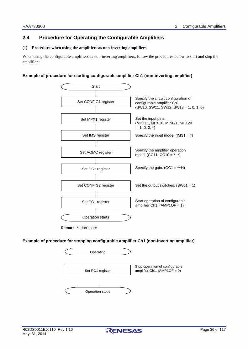
2.4 Procedure for Operating the Configurable Amplifiers
(1) Procedure when using the amplifiers as non-inverting amplifiers
When using the configurable amplifiers as non-inverting amplifiers, follow the procedures below to start and stop the amplifiers.
Example of procedure for starting configurable amplifier Ch1 (non-inverting amplifier)
Set the output switches. (SW01 = 1)
Start
Specify the circuit configuration of configurable amplifier Ch1.(SW10, SW11, SW12, SW13 = 1, 0, 1, 0)
Set the input pins.(MPX11, MPX10, MPX21, MPX20 = 1, 0, 0, *)
Remark *: don't care
Specify the gain. (GC1 = **H)
Start operation of configurable amplifier Ch1. (AMP1OF = 1)
Specify the amplifier operation mode. (CC11, CC10 = *, *)
Specify the input mode. (IMS1 = *)Set IMS register
Set CONFIG1 register
Set MPX1 register
Operation starts
Set PC1 register
Set CONFIG2 register
Set GC1 register
Set AOMC register
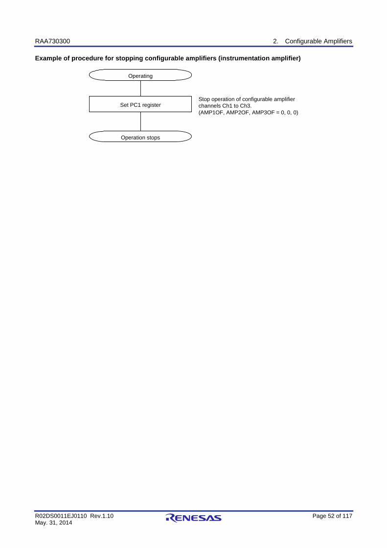
Example of procedure for stopping configurable amplifier Ch1 (non-inverting amplifier)
Operating
Set PC1 register
Operation stops
Stop operation of configurable amplifier Ch1. (AMP1OF = 0)

RAA730300 2. Configurable Amplifiers
R02DS0011EJ0110 Rev.1.10 Page 37 of 117 May. 31, 2014
Example of procedure for starting configurable amplifier Ch2 (non-inverting amplifier)
Example of procedure for stopping configurable amplifier Ch2 (non-inverting amplifier)
Operating
Set PC1 register
Operation stops
Stop operation of configurable amplifier Ch2. (AMP2OF = 0)
RAA730300 2. Configurable Amplifiers
R02DS0011EJ0110 Rev.1.10 Page 38 of 117 May. 31, 2014
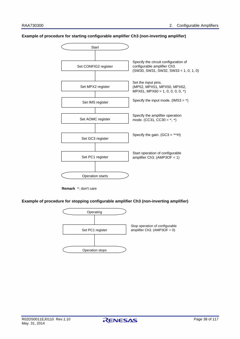
Example of procedure for starting configurable amplifier Ch3 (non-inverting amplifier)
Start
Set CONFIG2 registerSpecify the circuit configuration of configurable amplifier Ch3.(SW30, SW31, SW32, SW33 = 1, 0, 1, 0)
Set MPX2 registerSet the input pins.(MP52, MPX51, MPX50, MPX62, MPX61, MPX60 = 1, 0, 0, 0, 0, *)
Remark *: don't care
Set GC3 registerSpecify the gain. (GC3 = **H)
Set PC1 registerStart operation of configurable amplifier Ch3. (AMP3OF = 1)
Operation starts
Set AOMC registerSpecify the amplifier operation mode. (CC31, CC30 = *, *)
Specify the input mode. (IMS3 = *)Set IMS register
Example of procedure for stopping configurable amplifier Ch3 (non-inverting amplifier)
Operating
Set PC1 register
Operation stops
Stop operation of configurable amplifier Ch3. (AMP3OF = 0)
RAA730300 2. Configurable Amplifiers
R02DS0011EJ0110 Rev.1.10 Page 39 of 117 May. 31, 2014
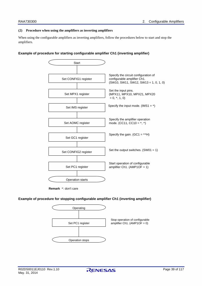
(2) Procedure when using the amplifiers as inverting amplifiers
When using the configurable amplifiers as inverting amplifiers, follow the procedures below to start and stop the amplifiers.
Example of procedure for starting configurable amplifier Ch1 (inverting amplifier)
Start
Set CONFIG1 registerSpecify the circuit configuration of configurable amplifier Ch1.(SW10, SW11, SW12, SW13 = 1, 0, 1, 0)
Set MPX1 registerSet the input pins.(MPX11, MPX10, MPX21, MPX20 = 0, *, 1, 0)
Remark *: don't care
Set GC1 registerSpecify the gain. (GC1 = **H)
Set CONFIG2 register Set the output switches. (SW01 = 1)
Set PC1 registerStart operation of configurable amplifier Ch1. (AMP1OF = 1)
Operation starts
Set AOMC registerSpecify the amplifier operation mode. (CC11, CC10 = *, *)
Specify the input mode. (IMS1 = *)Set IMS register
Example of procedure for stopping configurable amplifier Ch1 (inverting amplifier)
Operating
Set PC1 register
Operation stops
Stop operation of configurable amplifier Ch1. (AMP1OF = 0)
RAA730300 2. Configurable Amplifiers
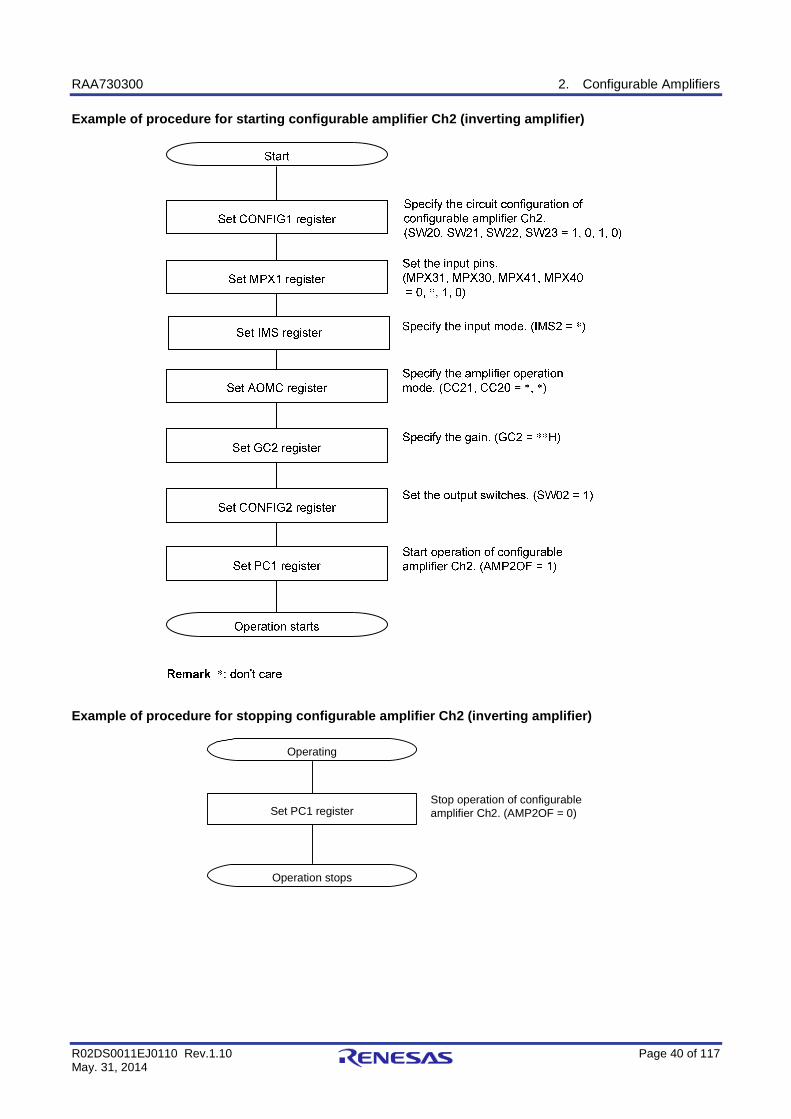
R02DS0011EJ0110 Rev.1.10 Page 40 of 117 May. 31, 2014
Example of procedure for starting configurable amplifier Ch2 (inverting amplifier)
Example of procedure for stopping configurable amplifier Ch2 (inverting amplifier)
Operating
Set PC1 register
Operation stops
Stop operation of configurable amplifier Ch2. (AMP2OF = 0)
RAA730300 2. Configurable Amplifiers
R02DS0011EJ0110 Rev.1.10 Page 41 of 117 May. 31, 2014
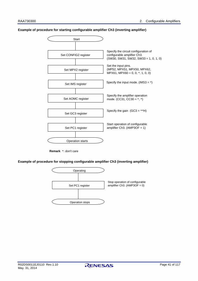
Example of procedure for starting configurable amplifier Ch3 (inverting amplifier)
Start
Set CONFIG2 registerSpecify the circuit configuration of configurable amplifier Ch3.(SW30, SW31, SW32, SW33 = 1, 0, 1, 0)
Set MPX2 registerSet the input pins.(MP52, MPX51, MPX50, MPX62, MPX61, MPX60 = 0, 0, *, 1, 0, 0)
Remark *: don't care
Set GC3 registerSpecify the gain (GC3 = **H)
Set PC1 registerStart operation of configurable amplifier Ch3. (AMP3OF = 1)
Operation starts
Set AOMC registerSpecify the amplifier operation mode. (CC31, CC30 = *, *)
Specify the input mode. (IMS3 = *)Set IMS register
Example of procedure for stopping configurable amplifier Ch3 (inverting amplifier)
Operating
Set PC1 register
Operation stops
Stop operation of configurable amplifier Ch3. (AMP3OF = 0)

RAA730300 2. Configurable Amplifiers
R02DS0011EJ0110 Rev.1.10 Page 42 of 117 May. 31, 2014
(3) Procedure when using the amplifiers as differential amplifiers
When using the configurable amplifiers together as a differential amplifier, follow the procedures below to start and stop the amplifier.
Example of procedure for starting configurable amplifier Ch1 (differential amplifier)
Start
Set CONFIG1 registerSpecify the circuit configuration of configurable amplifier Ch1.(SW10, SW11, SW12, SW13 = 1, 0, 0, 1)
Set MPX1 registerSet the input pins.(MPX11, MPX10, MPX21, MPX20 = 0, *, 0, *)
Remark *: don't care
Set GC1 registerSpecify the gain. (GC1 = **H)
Set CONFIG2 registerSet the output switches. (SW01 = 1)
Set PC1 registerStart operation of configurable amplifier Ch1. (AMP1OF = 1)
Operation starts
Set AOMC registerSpecify the amplifier operation mode. (CC11, CC10 = *, *)
Specify the input mode. (IMS1 = *)Set IMS register
Example of procedure for stopping configurable amplifier Ch1 (differential amplifier)
Operating
Set PC1 register
Operation stops
Stop operation of configurable amplifier Ch1. (AMP1OF = 0)

RAA730300 2. Configurable Amplifiers
R02DS0011EJ0110 Rev.1.10 Page 43 of 117 May. 31, 2014
Example of procedure for starting configurable amplifier Ch2 (differential amplifier)
Start
Set CONFIG1 registerSpecify the circuit configuration of configurable amplifier Ch2.(SW20, SW21, SW22, SW23 = 1, 0, 0, 1)
Set MPX1 registerSet the input pins.(MPX31, MPX30, MPX41, MPX40 = 0, *, 0, *)
Remark *: don't care
Set GC2 registerSpecify the gain. (GC2 = **H)
Set CONFIG2 registerSet the output switches. (SW02 = 1)
Set PC1 registerStart operation of configurable amplifier Ch2. (AMP2OF = 1)
Operation starts
Set AOMC registerSpecify the amplifier operation mode. (CC21, CC20 = *, *)
Specify the input mode. (IMS2 = *)Set IMS register
Example of procedure for stopping configurable amplifier Ch2 (differential amplifier)
Operating
Set PC1 register
Operation stops
Stop operation of configurable amplifier Ch2. (AMP2OF = 0)

RAA730300 2. Configurable Amplifiers
R02DS0011EJ0110 Rev.1.10 Page 44 of 117 May. 31, 2014
Example of procedure for starting configurable amplifier Ch3 (differential amplifier)
Start
Set CONFIG2 registerSpecify the circuit configuration of configurable amplifier Ch3.(SW30, SW31, SW32, SW33 = 1, 0, 0, 1)
Set MPX2 registerSet the input pins.(MP52, MPX51, MPX50, MPX62, MPX61, MPX60 = 0, 0, *, 0, 0, *)
Remark *: don't care
Set GC3 registerSpecify the gain. (GC3 = **H)
Set PC1 registerStart operation of configurable amplifier Ch3. (AMP3OF = 1)
Operation starts
Set AOMC registerSpecify the amplifier operation mode. (CC31, CC30 = *, *)
Specify the input mode. (IMS3 = *)Set IMS register
Example of procedure for stopping configurable amplifier Ch3 (differential amplifier)
Operating
Set PC1 register
Operation stops
Stop operation of configurable amplifier Ch3. (AMP3OF = 0)

RAA730300 2. Configurable Amplifiers
R02DS0011EJ0110 Rev.1.10 Page 45 of 117 May. 31, 2014
(4) Procedure when using the amplifiers as a transimpedance amplifier
When using the configurable amplifiers as transimpedance amplifiers, follow the procedures below to start and stop the amplifiers.
Example of procedure for starting configurable amplifier Ch1 (transimpedance amplifier)
Start
Set CONFIG1 registerSpecify the circuit configuration of configurable amplifier Ch1.(SW10, SW11, SW12, SW13 = 1, 1, 1, 0)
Set MPX1 registerSet the input pins.(MPX11, MPX10, MPX21, MPX20 = 0, *, 1, 0)
Remark *: don't care
Set GC1 registerSpecify the feedback resistance. (GC1 = **H)
Set CONFIG2 registerSet the output switches. (SW01 = 1)
Set PC1 registerStart operation of configurable amplifier Ch1. (AMP1OF = 1)
Operation starts
Set AOMC registerSpecify the amplifier operation mode. (CC11, CC10 = *, *)
Specify the input mode. (IMS1 = *)Set IMS register
Example of procedure for stopping configurable amplifier Ch1 (transimpedance amplifier)
Operating
Set PC1 register
Operation stops
Stop operation of configurable amplifier Ch1. (AMP1OF = 0)
RAA730300 2. Configurable Amplifiers
R02DS0011EJ0110 Rev.1.10 Page 46 of 117 May. 31, 2014
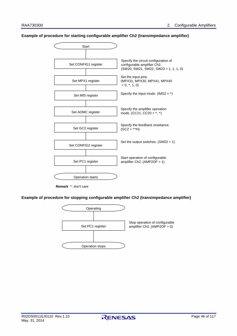
Example of procedure for starting configurable amplifier Ch2 (transimpedance amplifier)
Start
Set CONFIG1 registerSpecify the circuit configuration of configurable amplifier Ch2.(SW20, SW21, SW22, SW23 = 1, 1, 1, 0)
Set MPX1 registerSet the input pins.(MPX31, MPX30, MPX41, MPX40 = 0, *, 1, 0)
Remark *: don't care
Set GC2 registerSpecify the feedback resistance. (GC2 = **H)
Set CONFIG2 registerSet the output switches. (SW02 = 1)
Set PC1 registerStart operation of configurable amplifier Ch2. (AMP2OF = 1)
Operation starts
Set AOMC registerSpecify the amplifier operation mode. (CC21, CC20 = *, *)
Specify the input mode. (IMS2 = *)Set IMS register
Example of procedure for stopping configurable amplifier Ch2 (transimpedance amplifier)
Operating
Set PC1 register
Operation stops
Stop operation of configurable amplifier Ch2. (AMP2OF = 0)
RAA730300 2. Configurable Amplifiers
R02DS0011EJ0110 Rev.1.10 Page 47 of 117 May. 31, 2014
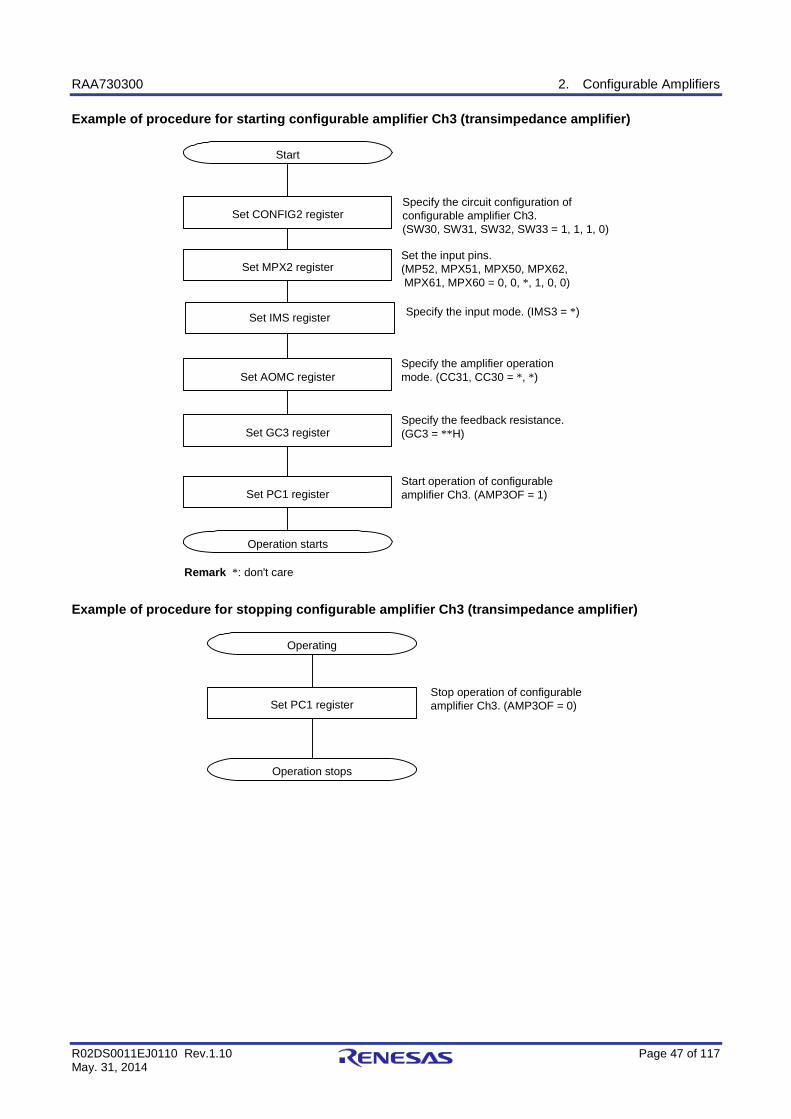
Example of procedure for starting configurable amplifier Ch3 (transimpedance amplifier)
Start
Set CONFIG2 registerSpecify the circuit configuration of configurable amplifier Ch3.(SW30, SW31, SW32, SW33 = 1, 1, 1, 0)
Set MPX2 registerSet the input pins.(MP52, MPX51, MPX50, MPX62, MPX61, MPX60 = 0, 0, *, 1, 0, 0)
Remark *: don't care
Set GC3 registerSpecify the feedback resistance. (GC3 = **H)
Set PC1 registerStart operation of configurable amplifier Ch3. (AMP3OF = 1)
Operation starts
Set AOMC registerSpecify the amplifier operation mode. (CC31, CC30 = *, *)
Specify the input mode. (IMS3 = *)Set IMS register
Example of procedure for stopping configurable amplifier Ch3 (transimpedance amplifier)
Operating
Set PC1 register
Operation stops
Stop operation of configurable amplifier Ch3. (AMP3OF = 0)
RAA730300 2. Configurable Amplifiers
R02DS0011EJ0110 Rev.1.10 Page 48 of 117 May. 31, 2014
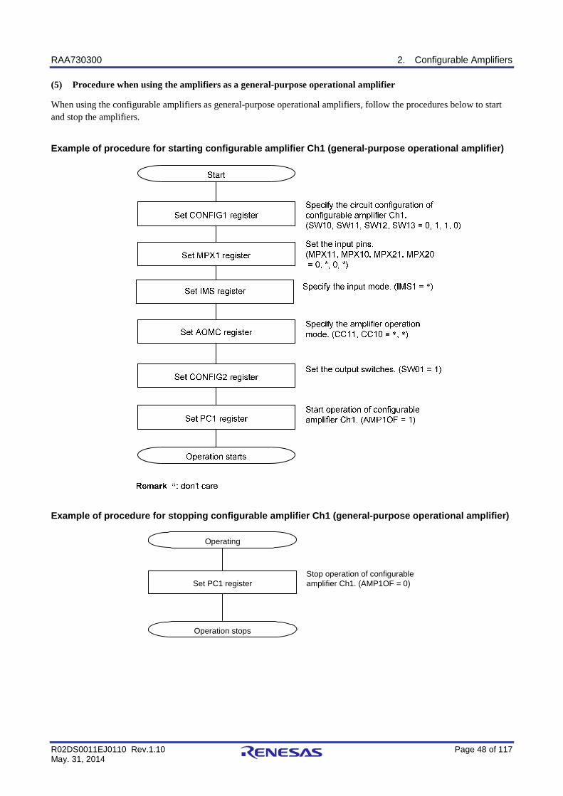
(5) Procedure when using the amplifiers as a general-purpose operational amplifier
When using the configurable amplifiers as general-purpose operational amplifiers, follow the procedures below to start and stop the amplifiers.
Example of procedure for starting configurable amplifier Ch1 (general-purpose operational amplifier)
Example of procedure for stopping configurable amplifier Ch1 (general-purpose operational amplifier)
Operating
Set PC1 register
Operation stops
Stop operation of configurable amplifier Ch1. (AMP1OF = 0)
RAA730300 2. Configurable Amplifiers
R02DS0011EJ0110 Rev.1.10 Page 49 of 117 May. 31, 2014
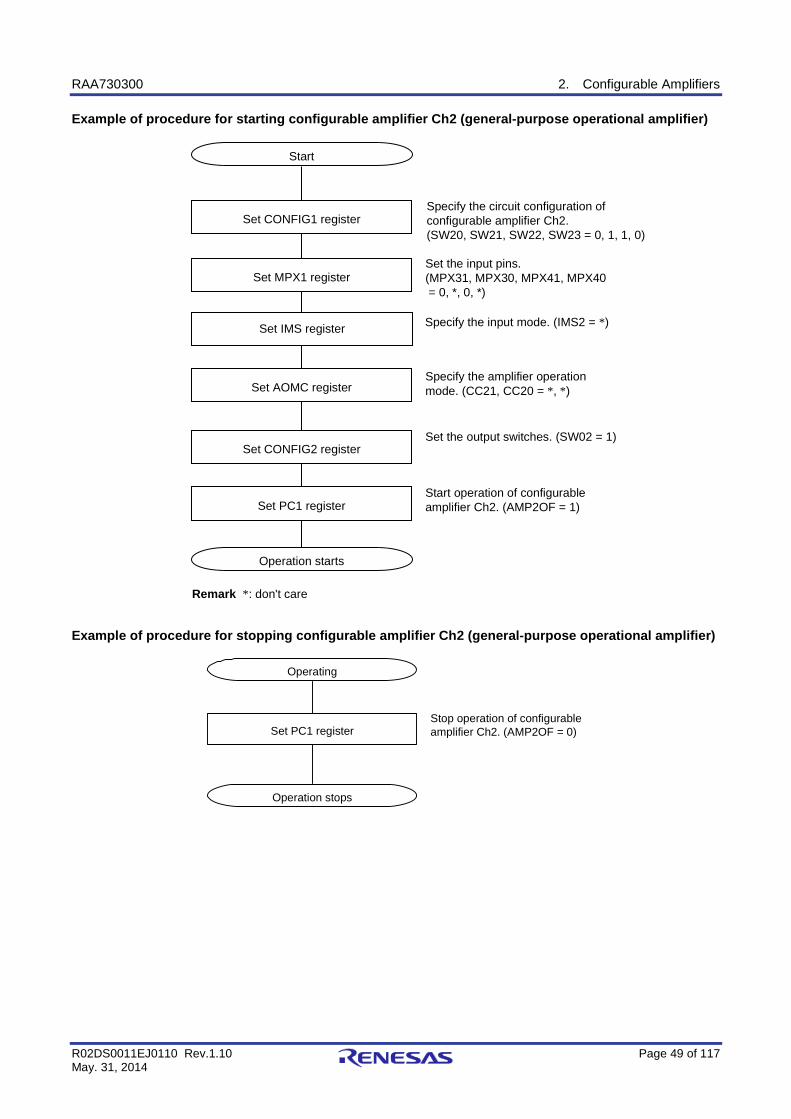
Example of procedure for starting configurable amplifier Ch2 (general-purpose operational amplifier)
Start
Set CONFIG1 registerSpecify the circuit configuration of configurable amplifier Ch2.(SW20, SW21, SW22, SW23 = 0, 1, 1, 0)
Set MPX1 registerSet the input pins.(MPX31, MPX30, MPX41, MPX40 = 0, *, 0, *)
Remark *: don't care
Set CONFIG2 registerSet the output switches. (SW02 = 1)
Set PC1 registerStart operation of configurable amplifier Ch2. (AMP2OF = 1)
Operation starts
Set AOMC registerSpecify the amplifier operation mode. (CC21, CC20 = *, *)
Specify the input mode. (IMS2 = *)Set IMS register
Example of procedure for stopping configurable amplifier Ch2 (general-purpose operational amplifier)
Operating
Set PC1 register
Operation stops
Stop operation of configurable amplifier Ch2. (AMP2OF = 0)
RAA730300 2. Configurable Amplifiers
R02DS0011EJ0110 Rev.1.10 Page 50 of 117 May. 31, 2014
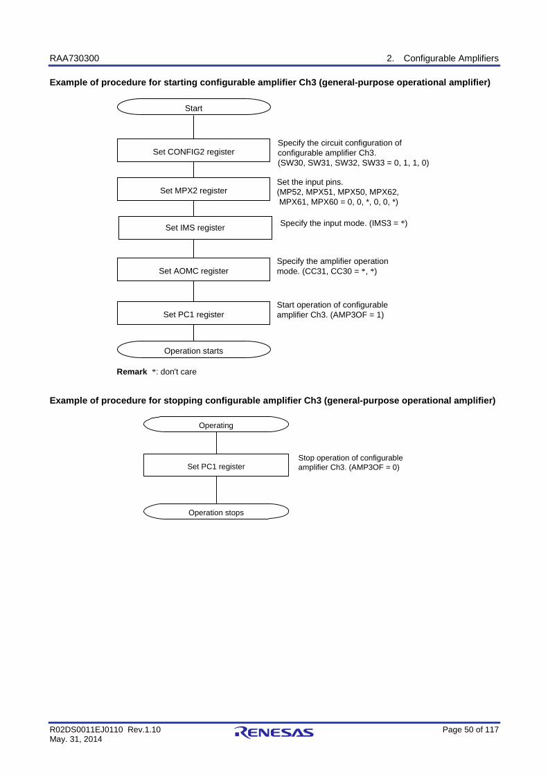
Example of procedure for starting configurable amplifier Ch3 (general-purpose operational amplifier)
Start
Set CONFIG2 registerSpecify the circuit configuration of configurable amplifier Ch3.(SW30, SW31, SW32, SW33 = 0, 1, 1, 0)
Set MPX2 registerSet the input pins.(MP52, MPX51, MPX50, MPX62, MPX61, MPX60 = 0, 0, *, 0, 0, *)
Remark *: don't care
Set PC1 registerStart operation of configurable amplifier Ch3. (AMP3OF = 1)
Operation starts
Set AOMC registerSpecify the amplifier operation mode. (CC31, CC30 = *, *)
Specify the input mode. (IMS3 = *)Set IMS register
Example of procedure for stopping configurable amplifier Ch3 (general-purpose operational amplifier)
Operating
Set PC1 register
Operation stops
Stop operation of configurable amplifier Ch3. (AMP3OF = 0)
RAA730300 2. Configurable Amplifiers
R02DS0011EJ0110 Rev.1.10 Page 51 of 117 May. 31, 2014
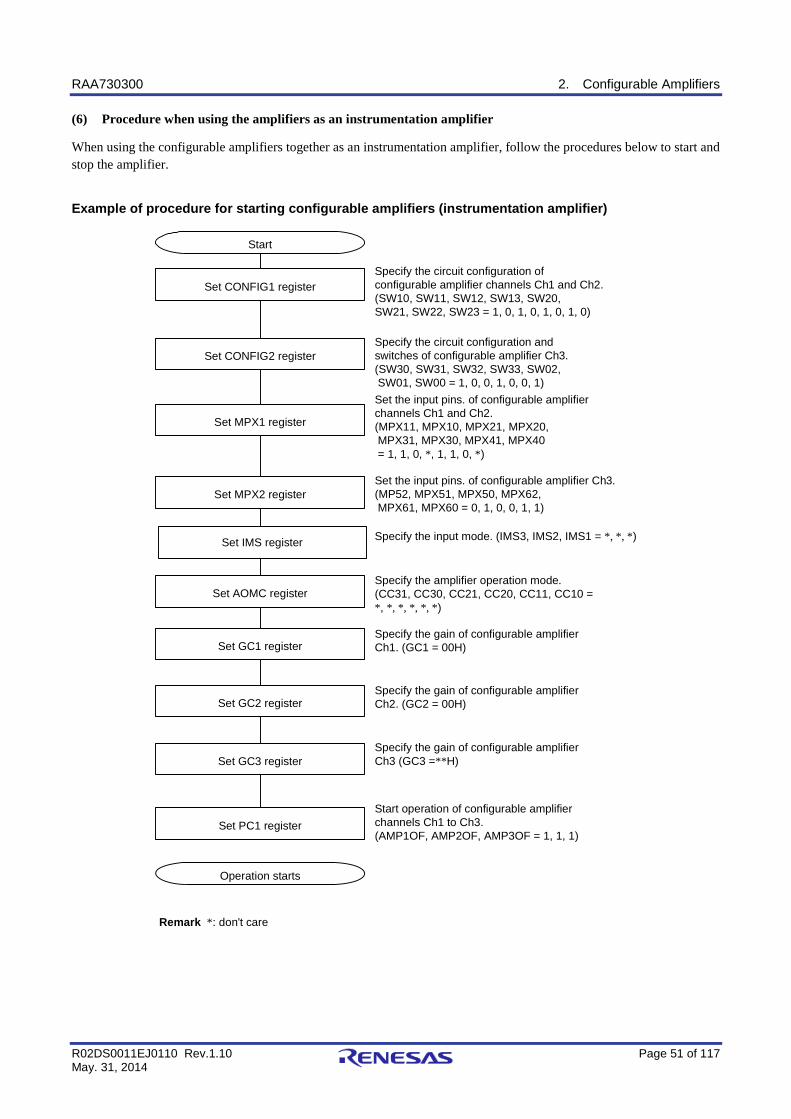
(6) Procedure when using the amplifiers as an instrumentation amplifier
When using the configurable amplifiers together as an instrumentation amplifier, follow the procedures below to start and stop the amplifier.
Example of procedure for starting configurable amplifiers (instrumentation amplifier)
Start
Set CONFIG1 registerSpecify the circuit configuration of configurable amplifier channels Ch1 and Ch2.(SW10, SW11, SW12, SW13, SW20,SW21, SW22, SW23 = 1, 0, 1, 0, 1, 0, 1, 0)
Set MPX1 register
Set the input pins. of configurable amplifier channels Ch1 and Ch2. (MPX11, MPX10, MPX21, MPX20, MPX31, MPX30, MPX41, MPX40 = 1, 1, 0, *, 1, 1, 0, *)
Remark *: don't care
Set GC1 registerSpecify the gain of configurable amplifier Ch1. (GC1 = 00H)
Set PC1 register
Operation starts
Set CONFIG2 registerSpecify the circuit configuration and switches of configurable amplifier Ch3.(SW30, SW31, SW32, SW33, SW02, SW01, SW00 = 1, 0, 0, 1, 0, 0, 1)
Set MPX2 registerSet the input pins. of configurable amplifier Ch3.(MP52, MPX51, MPX50, MPX62, MPX61, MPX60 = 0, 1, 0, 0, 1, 1)
Set GC2 registerSpecify the gain of configurable amplifier Ch2. (GC2 = 00H)
Set GC3 registerSpecify the gain of configurable amplifier Ch3 (GC3 =**H)
Set AOMC registerSpecify the amplifier operation mode. (CC31, CC30, CC21, CC20, CC11, CC10 = *, *, *, *, *, *)
Specify the input mode. (IMS3, IMS2, IMS1 = *, *, *)Set IMS register
Start operation of configurable amplifier channels Ch1 to Ch3. (AMP1OF, AMP2OF, AMP3OF = 1, 1, 1)
RAA730300 2. Configurable Amplifiers
R02DS0011EJ0110 Rev.1.10 Page 52 of 117 May. 31, 2014
Example of procedure for stopping configurable amplifiers (instrumentation amplifier)
Operating
Set PC1 register
Operation stops
Stop operation of configurable amplifier channels Ch1 to Ch3.(AMP1OF, AMP2OF, AMP3OF = 0, 0, 0)

RAA730300 3. General-Purpose Operational Amplifier
R02DS0011EJ0110 Rev.1.10 Page 53 of 117 May. 31, 2014
3. General-Purpose Operational Amplifier
The RAA730300 has two on-chip general-purpose operational amplifier channels.
3.1 Overview of General-Purpose Operational Amplifier Features
The general-purpose operational amplifiers have the following features:
• Includes an input mode switching function
• Includes a power-off function.
And also, the output signal from D/A converter Ch4 can be used as the reference voltage for a general-purpose operational amplifier Ch2. If D/A converter Ch4 is powered off, the external reference voltage is to be input to DAC4_OUT/VREFIN4 pin. For details about use of D/A converter, see 4. D/A Converter.
<R>
RAA730300 3. General-Purpose Operational Amplifier
R02DS0011EJ0110 Rev.1.10 Page 54 of 117 May. 31, 2014
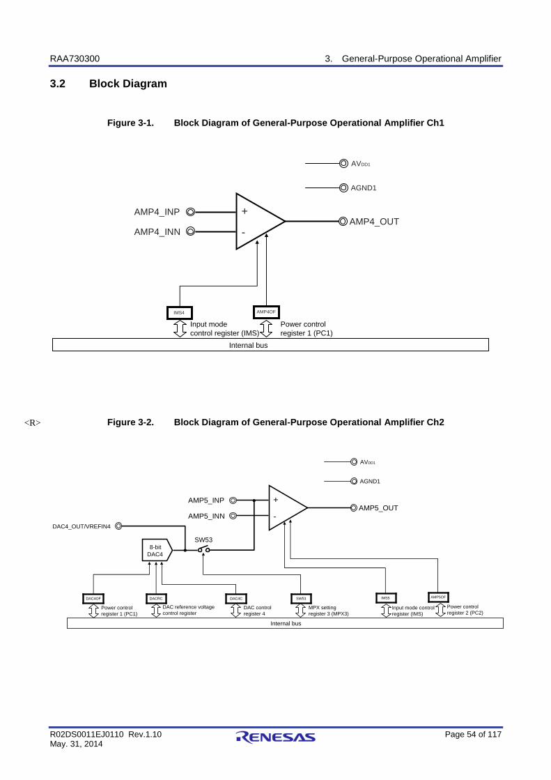
3.2 Block Diagram
Figure 3-1. Block Diagram of General-Purpose Operational Amplifier Ch1
+
-AMP4_OUT
AMP4_INN
AMP4_INP
AMP4OF
AVDD1
AGND1
IMS4
Power control register 1 (PC1)
Input mode control register (IMS)
Internal bus
Figure 3-2. Block Diagram of General-Purpose Operational Amplifier Ch2
+
-AMP5_OUT
AMP5_INN
AMP5_INP
AMP5OF
AVDD1
AGND1
IMS5
DAC4
SW53
DAC4_OUT/VREFIN4
Power control register 2 (PC2)
Input mode control register (IMS)
Internal bus
Power control register 1 (PC1)
DAC controlregister 4
DAC reference voltage control register
8-bit
DAC4OF DACRC DAC4C
MPX settingregister 3 (MPX3)
SW53
<R>
RAA730300 3. General-Purpose Operational Amplifier
R02DS0011EJ0110 Rev.1.10 Page 55 of 117 May. 31, 2014
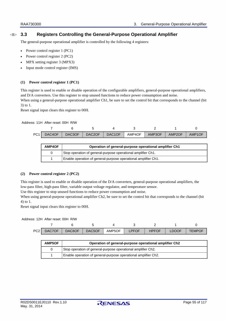
3.3 Registers Controlling the General-Purpose Operational Amplifier
The general-purpose operational amplifier is controlled by the following 4 registers:
• Power control register 1 (PC1) • Power control register 2 (PC2) • MPX setting register 3 (MPX3)
• Input mode control register (IMS)
(1) Power control register 1 (PC1)
This register is used to enable or disable operation of the configurable amplifiers, general-purpose operational amplifiers, and D/A converters. Use this register to stop unused functions to reduce power consumption and noise. When using a general-purpose operational amplifier Ch1, be sure to set the control bit that corresponds to the channel (bit 3) to 1. Reset signal input clears this register to 00H.
Address: 11H After reset: 00H R/W
7 6 5 4 3 2 1 0
PC1 DAC4OF DAC3OF DAC2OF DAC1OF AMP4OF AMP3OF AMP2OF AMP1OF
AMP4OF Operation of general-purpose operational amplifier Ch1
0 Stop operation of general-purpose operational amplifier Ch1.
1 Enable operation of general-purpose operational amplifier Ch1.
(2) Power control register 2 (PC2)
This register is used to enable or disable operation of the D/A converters, general-purpose operational amplifiers, the low-pass filter, high-pass filter, variable output voltage regulator, and temperature sensor. Use this register to stop unused functions to reduce power consumption and noise. When using general-purpose operational amplifier Ch2, be sure to set the control bit that corresponds to the channel (bit 4) to 1. Reset signal input clears this register to 00H.
Address: 12H After reset: 00H R/W
7 6 5 4 3 2 1 0
PC2 DAC7OF DAC6OF DAC5OF AMP5OF LPFOF HPFOF LDOOF TEMPOF
AMP5OF Operation of general-purpose operational amplifier Ch2
0 Stop operation of general-purpose operational amplifier Ch2.
1 Enable operation of general-purpose operational amplifier Ch2.
<R>
RAA730300 3. General-Purpose Operational Amplifier
R02DS0011EJ0110 Rev.1.10 Page 56 of 117 May. 31, 2014
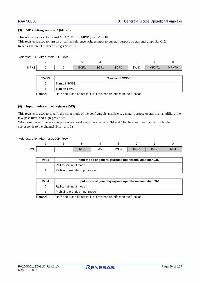
(3) MPX setting register 3 (MPX3)
This register is used to control MPX7, MPX8, MPX9, and MPX10. This register is used to turn on or off the reference voltage input to general-purpose operational amplifier Ch2. Reset signal input clears this register to 00H.
Address: 05H After reset: 00H R/W
7 6 5 4 3 2 1 0
MPX3 0 0 SCF2 SCF1 SCF0 SW53 MPX71 MPX70
SW53 Control of SW53
0 Turn off SW53.
1 Turn on SW53.
Remark Bits 7 and 6 can be set to 1, but this has no effect on the function.
(4) Input mode control register (IMS)
This register is used to specify the input mode of the configurable amplifiers, general-purpose operational amplifiers, the low-pass filter, and high-pass filter. When using one of general-purpose operational amplifier channels Ch1 and Ch2, be sure to set the control bit that corresponds to the channel (bits 4 and 3).
Address: 14H After reset: 00H R/W
7 6 5 4 3 2 1 0
IMS 0 0 IMS6 IMS5 IMS4 IMS3 IMS2 IMS1
IMS5 Input mode of general-purpose operational amplifier Ch2
0 Rail-to-rail input mode
1 P-ch single-ended input mode
IMS4 Input mode of general-purpose operational amplifier Ch1
0 Rail-to-rail input mode
1 P-ch single-ended input mode
Remark Bits 7 and 6 can be set to 1, but this has no effect on the function.

RAA730300 3. General-Purpose Operational Amplifier
R02DS0011EJ0110 Rev.1.10 Page 57 of 117 May. 31, 2014
3.4 Procedure for Operating the General-Purpose Operational Amplifier
Follow the procedures below to start and stop the general-purpose operational amplifier.
Example of procedure for starting the general-purpose operational amplifier Ch1
Start
Set PC1 register
Operation starts
Set IMS register Specify the input mode.(IMS4 = *)
Start operation of the general-purpose operationalamplifier. (AMP4OF = 1)
Example of procedure for stopping the general-purpose operational amplifier Ch1
Operating
Set PC1 register
Operation stops
Stop operation of the general-purpose operationalamplifier. (AMP4OF = 0)
RAA730300 3. General-Purpose Operational Amplifier
R02DS0011EJ0110 Rev.1.10 Page 58 of 117 May. 31, 2014
Example of procedure for starting the general-purpose operational amplifier Ch2
Start
Set PC2 register
Operation starts
Set IMS register
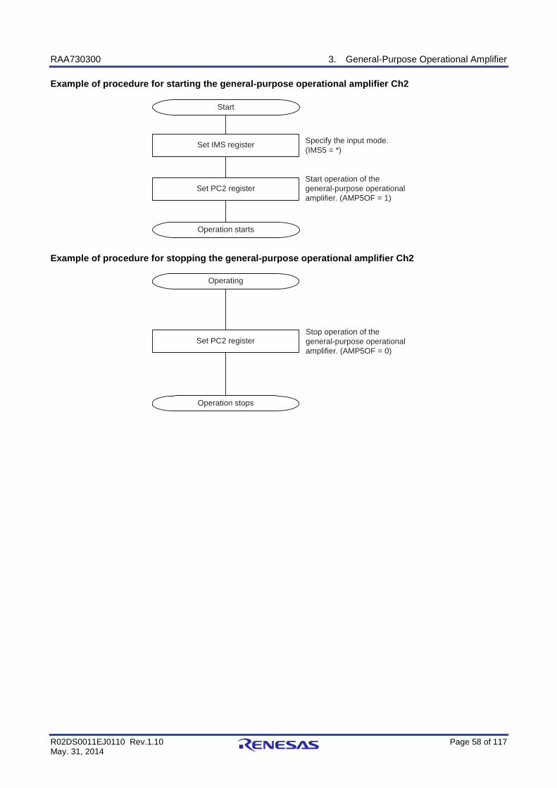
Start operation of the general-purpose operationalamplifier. (AMP5OF = 1)
Specify the input mode.(IMS5 = *)
Example of procedure for stopping the general-purpose operational amplifier Ch2
Operating
Set PC2 register
Operation stops
Stop operation of the general-purpose operationalamplifier. (AMP5OF = 0)

RAA730300 4. D/A Converters
R02DS0011EJ0110 Rev.1.10 Page 59 of 117 May. 31, 2014
4. D/A Converters
The RAA730300 has seven on-chip D/A converter channels.
Channel D/A Converter Output Pins
1 to 4 Provided
5 to 7 Not provided Note Note Output pins are not provided although the channels are incorporated.
4.1 Overview of D/A Converter Features
The D/A converters are 8-bit resolution converters that convert digital input signals into analog signals. The D/A converters have the following features:
• 8-bit resolution (× 7 ch: Ch1 to Ch7)
• R-2R ladder method
• Analog output voltage: Output voltage can be calculated with the equation shown below.
Output voltage = {(Reference voltage upper limit – Reference voltage lower limit) × m/256}
+ Reference voltage lower limit (m = 0 to 255: Value set to DACnC register)
• Controls the reference voltage for the configurable amplifier channels, general-purpose operational amplifier Ch2, low-pass filter, and high-pass filter
• Includes a power-off function.
Remark n = 1 to 7
<R>
RAA730300 4. D/A Converters
R02DS0011EJ0110 Rev.1.10 Page 60 of 117 May. 31, 2014
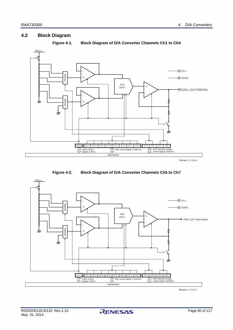
4.2 Block Diagram
Figure 4-1. Block Diagram of D/A Converter Channels Ch1 to Ch4
AVDD1
+
-
+
-
DACn +
-DACn_OUT/VREFINn
VRB0VRT0 VRB1VRT1DACnOF
AVDD1
AGND1
DACn2 DACn1DACn4 DACn3 0nCAD5nCAD6nCADDACn7
Power control register 1 (PC1)
DAC control register n (DACnC) DAC reference voltage control register (DACRC)
Internal bus
8-bit
Selector
Selector
Remark n = 1 to 4
Figure 4-2. Block Diagram of D/A Converter Channels Ch5 to Ch7
AVDD1
+
-
+
-
DACn +
-
VRB0VRT0 VRB1VRT1DACnOF
AVDD1
AGND1
DACn2 DACn1DACn4 DACn3 0nCAD5nCAD6nCADDACn7
Power control register 2 (PC2)
DAC control register n (DACnC) DAC reference voltage control register (DACRC)
Internal bus
8-bit
Selector
Selector
Remark n = 5 to 7
DACn_OUT output signal
RAA730300 4. D/A Converters
R02DS0011EJ0110 Rev.1.10 Page 61 of 117 May. 31, 2014
4.3 Registers Controlling the D/A Converters The D/A converters are controlled by the following 4 registers:
• DAC reference voltage control register (DACRC)
• DAC control registers 1, 2, 3, 4, 5, 6, 7 (DAC1C, DAC2C, DAC3C, DAC4C, DAC5C, DAC6C, DAC7C)
• Power control register 1 (PC1)
• Power control register 2 (PC2)
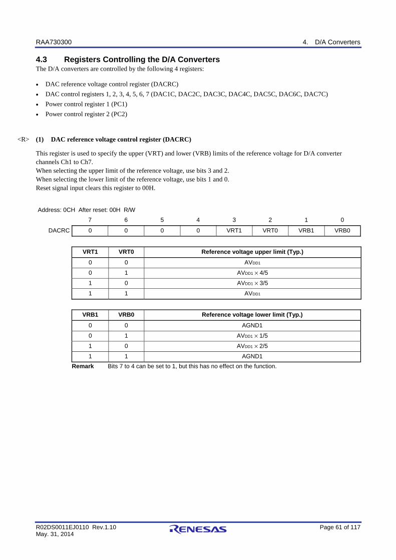
(1) DAC reference voltage control register (DACRC)
This register is used to specify the upper (VRT) and lower (VRB) limits of the reference voltage for D/A converter channels Ch1 to Ch7. When selecting the upper limit of the reference voltage, use bits 3 and 2. When selecting the lower limit of the reference voltage, use bits 1 and 0. Reset signal input clears this register to 00H.
Address: 0CH After reset: 00H R/W
7 6 5 4 3 2 1 0
DACRC 0 0 0 0 VRT1 VRT0 VRB1 VRB0
VRT1 VRT0 Reference voltage upper limit (Typ.)
0 0 AVDD1
0 1 AVDD1 × 4/5
1 0 AVDD1 × 3/5
1 1 AVDD1
VRB1 VRB0 Reference voltage lower limit (Typ.)
0 0 AGND1
0 1 AVDD1 × 1/5
1 0 AVDD1 × 2/5
1 1 AGND1 Remark Bits 7 to 4 can be set to 1, but this has no effect on the function.
<R>
RAA730300 4. D/A Converters
R02DS0011EJ0110 Rev.1.10 Page 62 of 117 May. 31, 2014
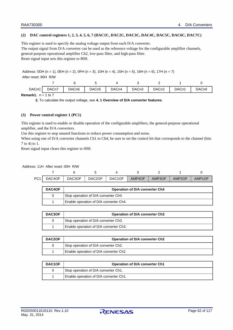
(2) DAC control registers 1, 2, 3, 4, 5, 6, 7 (DAC1C, DAC2C, DAC3C, DAC4C, DAC5C, DAC6C, DAC7C)
This register is used to specify the analog voltage output from each D/A converter. The output signal from D/A converter can be used as the reference voltage for the configurable amplifier channels, general-purpose operational amplifier Ch2, low-pass filter, and high-pass filter. Reset signal input sets this register to 80H.
Address: 0DH (n = 1), 0EH (n = 2), 0FH (n = 3), 10H (n = 4), 15H (n = 5), 16H (n = 6), 17H (n = 7) After reset: 80H R/W
7 6 5 4 3 2 1 0
DACnC DACn7 DACn6 DACn5 DACn4 DACn3 DACn2 DACn1 DACn0 Remark1. n = 1 to 7
2. To calculate the output voltage, see 4. 1 Overview of D/A converter features.
(3) Power control register 1 (PC1)
This register is used to enable or disable operation of the configurable amplifiers, the general-purpose operational amplifier, and the D/A converters. Use this register to stop unused functions to reduce power consumption and noise. When using one of D/A converter channels Ch1 to Ch4, be sure to set the control bit that corresponds to the channel (bits 7 to 4) to 1. Reset signal input clears this register to 00H.
Address: 11H After reset: 00H R/W
7 6 5 4 3 2 1 0
PC1 DAC4OF DAC3OF DAC2OF DAC1OF AMP4OF AMP3OF AMP2OF AMP1OF
DAC4OF Operation of D/A converter Ch4
0 Stop operation of D/A converter Ch4.
1 Enable operation of D/A converter Ch4.
DAC3OF Operation of D/A converter Ch3
0 Stop operation of D/A converter Ch3.
1 Enable operation of D/A converter Ch3.
DAC2OF Operation of D/A converter Ch2
0 Stop operation of D/A converter Ch2.
1 Enable operation of D/A converter Ch2.
DAC1OF Operation of D/A converter Ch1
0 Stop operation of D/A converter Ch1.
1 Enable operation of D/A converter Ch1.
RAA730300 4. D/A Converters
R02DS0011EJ0110 Rev.1.10 Page 63 of 117 May. 31, 2014
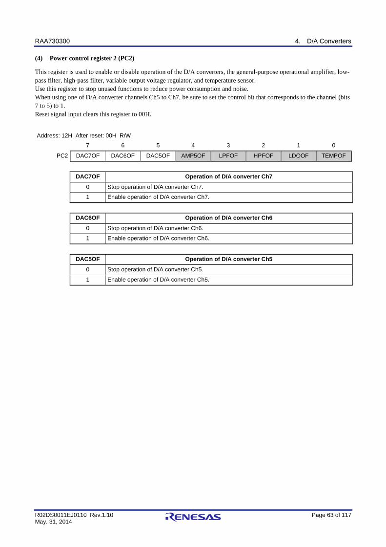
(4) Power control register 2 (PC2)
This register is used to enable or disable operation of the D/A converters, the general-purpose operational amplifier, low-pass filter, high-pass filter, variable output voltage regulator, and temperature sensor. Use this register to stop unused functions to reduce power consumption and noise. When using one of D/A converter channels Ch5 to Ch7, be sure to set the control bit that corresponds to the channel (bits 7 to 5) to 1. Reset signal input clears this register to 00H.
Address: 12H After reset: 00H R/W
7 6 5 4 3 2 1 0
PC2 DAC7OF DAC6OF DAC5OF AMP5OF LPFOF HPFOF LDOOF TEMPOF
DAC7OF Operation of D/A converter Ch7
0 Stop operation of D/A converter Ch7.
1 Enable operation of D/A converter Ch7.
DAC6OF Operation of D/A converter Ch6
0 Stop operation of D/A converter Ch6.
1 Enable operation of D/A converter Ch6.
DAC5OF Operation of D/A converter Ch5
0 Stop operation of D/A converter Ch5.
1 Enable operation of D/A converter Ch5.
RAA730300 4. D/A Converters
R02DS0011EJ0110 Rev.1.10 Page 64 of 117 May. 31, 2014
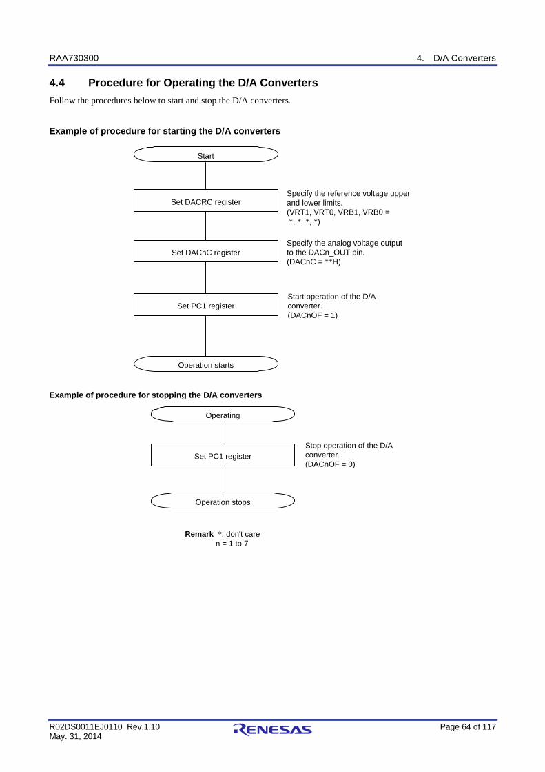
4.4 Procedure for Operating the D/A Converters
Follow the procedures below to start and stop the D/A converters.
Example of procedure for starting the D/A converters
Start
Set DACRC registerSpecify the reference voltage upper and lower limits.(VRT1, VRT0, VRB1, VRB0 = *, *, *, *)
Set DACnC registerSpecify the analog voltage output to the DACn_OUT pin. (DACnC = **H)
Set PC1 registerStart operation of the D/A converter. (DACnOF = 1)
Operation starts
Example of procedure for stopping the D/A converters
Remark *: don't caren = 1 to 7
Operating
Set PC1 register
Operation stops
Stop operation of the D/A converter. (DACnOF = 0)
RAA730300 4. D/A Converters
R02DS0011EJ0110 Rev.1.10 Page 65 of 117 May. 31, 2014
4.5 Notes on Using D/A Converters
Observe the following points when using the D/A converters:
(1) Only a very small current can flow from the DACn_OUT pin because the output impedance of the D/A converters is
high. If the load input impedance is low, insert a follower amplifier between the load and the DACn_OUT pin. Also, make sure that the wiring between the pin and the follower amplifier or load is as short as possible (because of the high output impedance). If it is not possible to keep the wiring short, take measures such as surrounding the pin with a ground pattern.
(2) If inputting an external reference power supply to the VREFINn pin, be sure to set the DACnOF bit to 0.
Remark n = 1 to 4
RAA730300 5. Low-Pass Filter
R02DS0011EJ0110 Rev.1.10 Page 66 of 117 May. 31, 2014
5. Low-Pass Filter
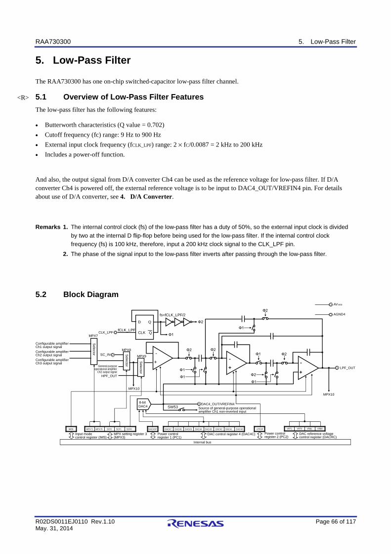
The RAA730300 has one on-chip switched-capacitor low-pass filter channel.
5.1 Overview of Low-Pass Filter Features
The low-pass filter has the following features:
• Butterworth characteristics (Q value = 0.702)
• Cutoff frequency (fc) range: 9 Hz to 900 Hz
• External input clock frequency (fCLK_LPF) range: 2 × fC/0.0087 = 2 kHz to 200 kHz
• Includes a power-off function.
And also, the output signal from D/A converter Ch4 can be used as the reference voltage for low-pass filter. If D/A converter Ch4 is powered off, the external reference voltage is to be input to DAC4_OUT/VREFIN4 pin. For details about use of D/A converter, see 4. D/A Converter.
Remarks 1. The internal control clock (fs) of the low-pass filter has a duty of 50%, so the external input clock is divided by two at the internal D flip-flop before being used for the low-pass filter. If the internal control clock frequency (fs) is 100 kHz, therefore, input a 200 kHz clock signal to the CLK_LPF pin.
2. The phase of the signal input to the low-pass filter inverts after passing through the low-pass filter.
5.2 Block Diagram
+
-
+ -
+
-
D Q
QCLK
fs=fCLK_LPF/2
MPX8SC_IN
CLK_LPF
DAC4
MPX9
HPF_OUT
MPX10
LPF_OUT
DAC4_OUT/VREFIN4
LPFOF DAC4OF MPX71 MPX70 SCF1 SCF0SCF2
AVDD3
AGND4
VRB0VRT0 VRB1VRT1DAC42 DAC41DAC44 DAC43 04CAD54CAD64CADDAC47
fCLK_LPFMPX7
IMS6
MPX setting register 3 (MPX3)
Power control register 1 (PC1)
DAC control register 4 (DAC4C) DAC reference voltage control register (DACRC)
Input mode control register (IMS)
8-bit
Source of general-purpose operationalamplifier Ch1 non-inverted input
Selector S
elector
Selector
Power control register 2 (PC2)
Configurable amplifierCh1 output signal
Internal bus
Configurable amplifierCh2 output signalConfigurable amplifierCh3 output signal
General-purpose operational amplifier
Ch2 output signal
SW53
MPX10
<R>
RAA730300 5. Low-Pass Filter
R02DS0011EJ0110 Rev.1.10 Page 67 of 117 May. 31, 2014
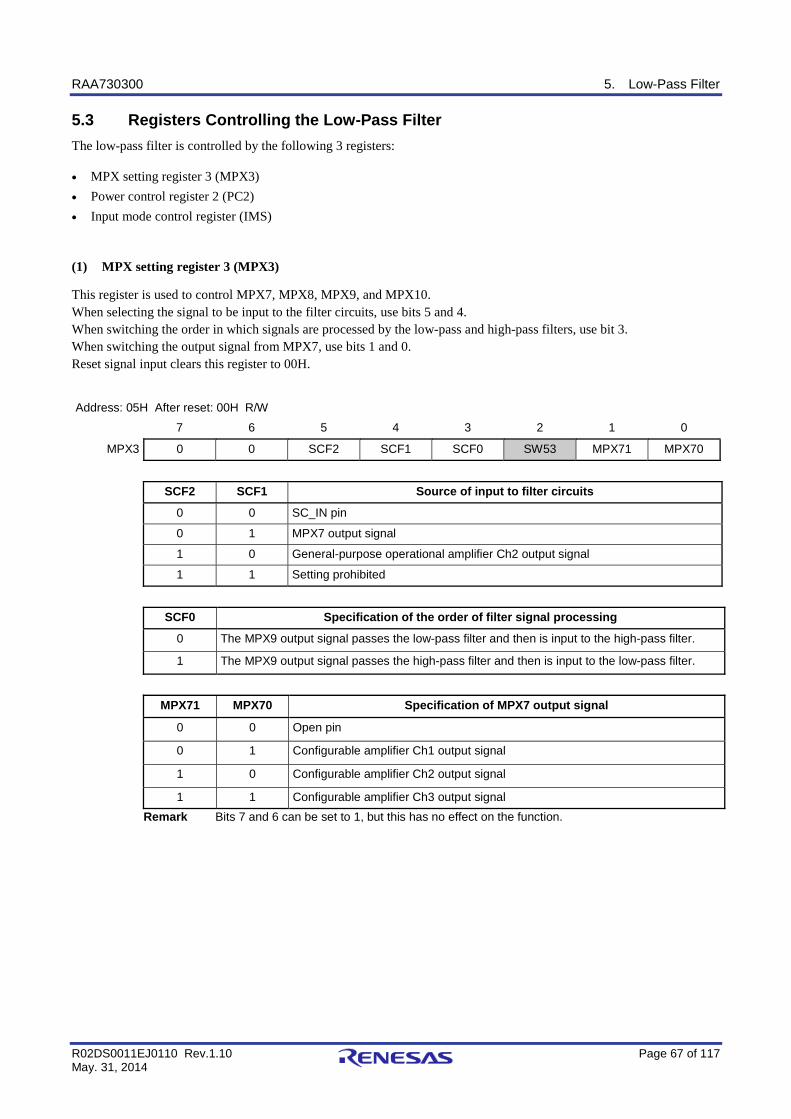
5.3 Registers Controlling the Low-Pass Filter
The low-pass filter is controlled by the following 3 registers:
• MPX setting register 3 (MPX3)
• Power control register 2 (PC2)
• Input mode control register (IMS)
(1) MPX setting register 3 (MPX3)
This register is used to control MPX7, MPX8, MPX9, and MPX10. When selecting the signal to be input to the filter circuits, use bits 5 and 4. When switching the order in which signals are processed by the low-pass and high-pass filters, use bit 3. When switching the output signal from MPX7, use bits 1 and 0. Reset signal input clears this register to 00H.
Address: 05H After reset: 00H R/W
7 6 5 4 3 2 1 0
MPX3 0 0 SCF2 SCF1 SCF0 SW53 MPX71 MPX70
SCF2 SCF1 Source of input to filter circuits
0 0 SC_IN pin
0 1 MPX7 output signal
1 0 General-purpose operational amplifier Ch2 output signal
1 1 Setting prohibited
SCF0 Specification of the order of filter signal processing
0 The MPX9 output signal passes the low-pass filter and then is input to the high-pass filter.
1 The MPX9 output signal passes the high-pass filter and then is input to the low-pass filter.
MPX71 MPX70 Specification of MPX7 output signal
0 0 Open pin
0 1 Configurable amplifier Ch1 output signal
1 0 Configurable amplifier Ch2 output signal
1 1 Configurable amplifier Ch3 output signal Remark Bits 7 and 6 can be set to 1, but this has no effect on the function.
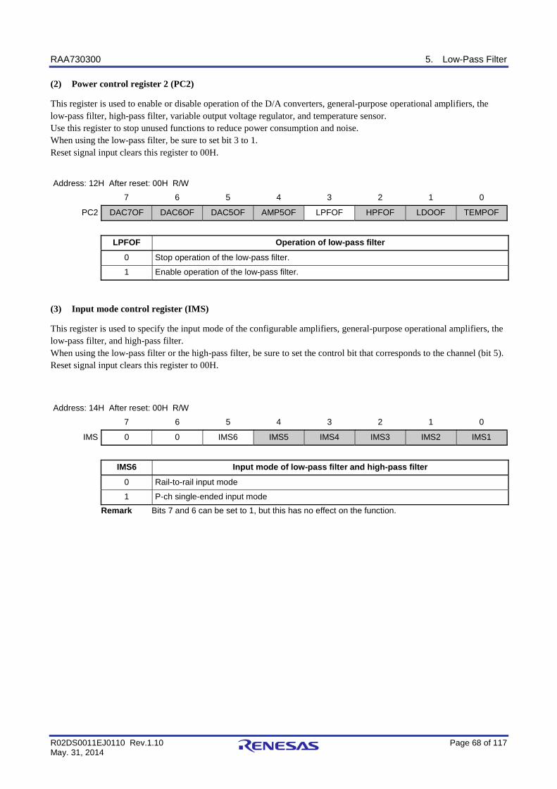
RAA730300 5. Low-Pass Filter
R02DS0011EJ0110 Rev.1.10 Page 68 of 117 May. 31, 2014
(2) Power control register 2 (PC2)
This register is used to enable or disable operation of the D/A converters, general-purpose operational amplifiers, the low-pass filter, high-pass filter, variable output voltage regulator, and temperature sensor. Use this register to stop unused functions to reduce power consumption and noise. When using the low-pass filter, be sure to set bit 3 to 1. Reset signal input clears this register to 00H.
Address: 12H After reset: 00H R/W
7 6 5 4 3 2 1 0
PC2 DAC7OF DAC6OF DAC5OF AMP5OF LPFOF HPFOF LDOOF TEMPOF
LPFOF Operation of low-pass filter
0 Stop operation of the low-pass filter.
1 Enable operation of the low-pass filter.
(3) Input mode control register (IMS)
This register is used to specify the input mode of the configurable amplifiers, general-purpose operational amplifiers, the low-pass filter, and high-pass filter. When using the low-pass filter or the high-pass filter, be sure to set the control bit that corresponds to the channel (bit 5). Reset signal input clears this register to 00H.
Address: 14H After reset: 00H R/W
7 6 5 4 3 2 1 0
IMS 0 0 IMS6 IMS5 IMS4 IMS3 IMS2 IMS1
IMS6 Input mode of low-pass filter and high-pass filter
0 Rail-to-rail input mode
1 P-ch single-ended input mode Remark Bits 7 and 6 can be set to 1, but this has no effect on the function.
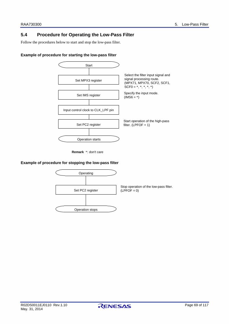
RAA730300 5. Low-Pass Filter
R02DS0011EJ0110 Rev.1.10 Page 69 of 117 May. 31, 2014
5.4 Procedure for Operating the Low-Pass Filter
Follow the procedures below to start and stop the low-pass filter.
Example of procedure for starting the low-pass filter
Start
Set MPX3 register
Remark *: don't care
Set PC2 registerStart operation of the high-pass filter. (LPFOF = 1)
Operation starts
Input control clock to CLK_LPF pin
Set IMS register Specify the input mode. (IMS6 = *)
Select the filter input signal and signal processing route.(MPX71, MPX70, SCF2, SCF1, SCF0 = *, *, *, *, *)
Example of procedure for stopping the low-pass filter
Operating
Set PC2 register
Operation stops
Stop operation of the low-pass filter. (LPFOF = 0)
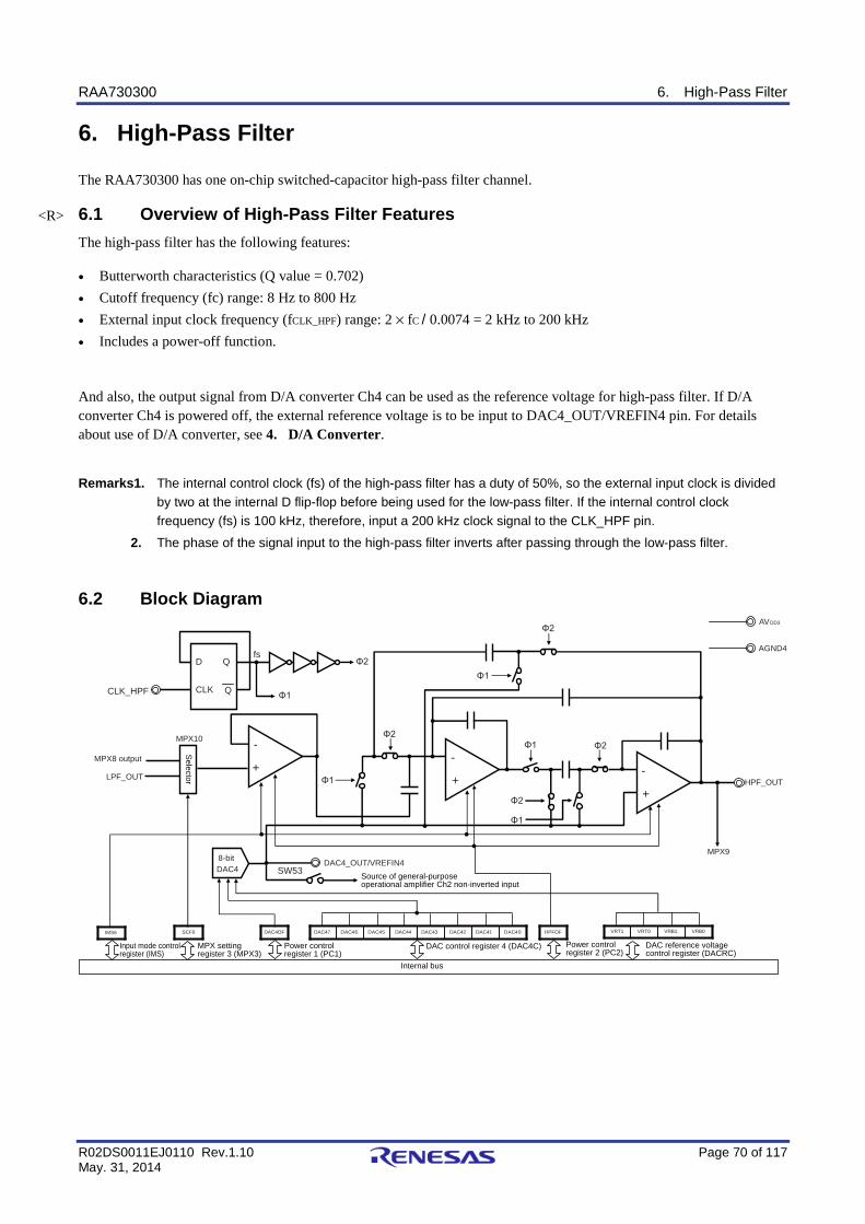
RAA730300 6. High-Pass Filter
R02DS0011EJ0110 Rev.1.10 Page 70 of 117 May. 31, 2014
6. High-Pass Filter
The RAA730300 has one on-chip switched-capacitor high-pass filter channel.
6.1 Overview of High-Pass Filter Features
The high-pass filter has the following features:
• Butterworth characteristics (Q value = 0.702)
• Cutoff frequency (fc) range: 8 Hz to 800 Hz
• External input clock frequency (fCLK_HPF) range: 2 × fC / 0.0074 = 2 kHz to 200 kHz
• Includes a power-off function.
And also, the output signal from D/A converter Ch4 can be used as the reference voltage for high-pass filter. If D/A converter Ch4 is powered off, the external reference voltage is to be input to DAC4_OUT/VREFIN4 pin. For details about use of D/A converter, see 4. D/A Converter.
Remarks1. The internal control clock (fs) of the high-pass filter has a duty of 50%, so the external input clock is divided
by two at the internal D flip-flop before being used for the low-pass filter. If the internal control clock frequency (fs) is 100 kHz, therefore, input a 200 kHz clock signal to the CLK_HPF pin.
2. The phase of the signal input to the high-pass filter inverts after passing through the low-pass filter.
6.2 Block Diagram
CLK_HPF
+
-
+
-
+
-
D Q
QCLK
fs
DAC4
MPX10
LPF_OUT
DAC4_OUT/VREFIN4
HPF_OUT
MPX9
HPFOF DAC4OF SCF0
AVDD3
AGND4
VRB0VRT0 VRB1VRT1DAC42 DAC41DAC44 DAC43 04CAD54CAD64CADDAC47IMS6
MPX setting register 3 (MPX3)
Power control register 1 (PC1)
DAC control register 4 (DAC4C) DAC reference voltage control register (DACRC)
Input mode control register (IMS)
8-bit
Source of general-purposeoperational amplifier Ch2 non-inverted input
Selector
Power control register 2 (PC2)
Internal bus
MPX8 output
SW53
<R>
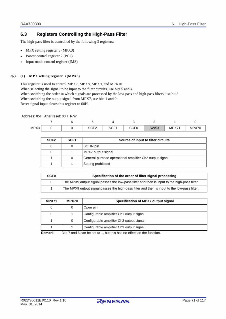
RAA730300 6. High-Pass Filter
R02DS0011EJ0110 Rev.1.10 Page 71 of 117 May. 31, 2014
6.3 Registers Controlling the High-Pass Filter
The high-pass filter is controlled by the following 3 registers:
• MPX setting register 3 (MPX3)
• Power control register 2 (PC2)
• Input mode control register (IMS)
(1) MPX setting register 3 (MPX3)
This register is used to control MPX7, MPX8, MPX9, and MPX10. When selecting the signal to be input to the filter circuits, use bits 5 and 4. When switching the order in which signals are processed by the low-pass and high-pass filters, use bit 3. When switching the output signal from MPX7, use bits 1 and 0. Reset signal input clears this register to 00H.
Address: 05H After reset: 00H R/W
7 6 5 4 3 2 1 0
MPX3 0 0 SCF2 SCF1 SCF0 SW53 MPX71 MPX70
SCF2 SCF1 Source of input to filter circuits
0 0 SC_IN pin
0 1 MPX7 output signal
1 0 General-purpose operational amplifier Ch2 output signal
1 1 Setting prohibited
SCF0 Specification of the order of filter signal processing
0 The MPX9 output signal passes the low-pass filter and then is input to the high-pass filter.
1 The MPX9 output signal passes the high-pass filter and then is input to the low-pass filter.
MPX71 MPX70 Specification of MPX7 output signal
0 0 Open pin
0 1 Configurable amplifier Ch1 output signal
1 0 Configurable amplifier Ch2 output signal
1 1 Configurable amplifier Ch3 output signal Remark Bits 7 and 6 can be set to 1, but this has no effect on the function.
<R>
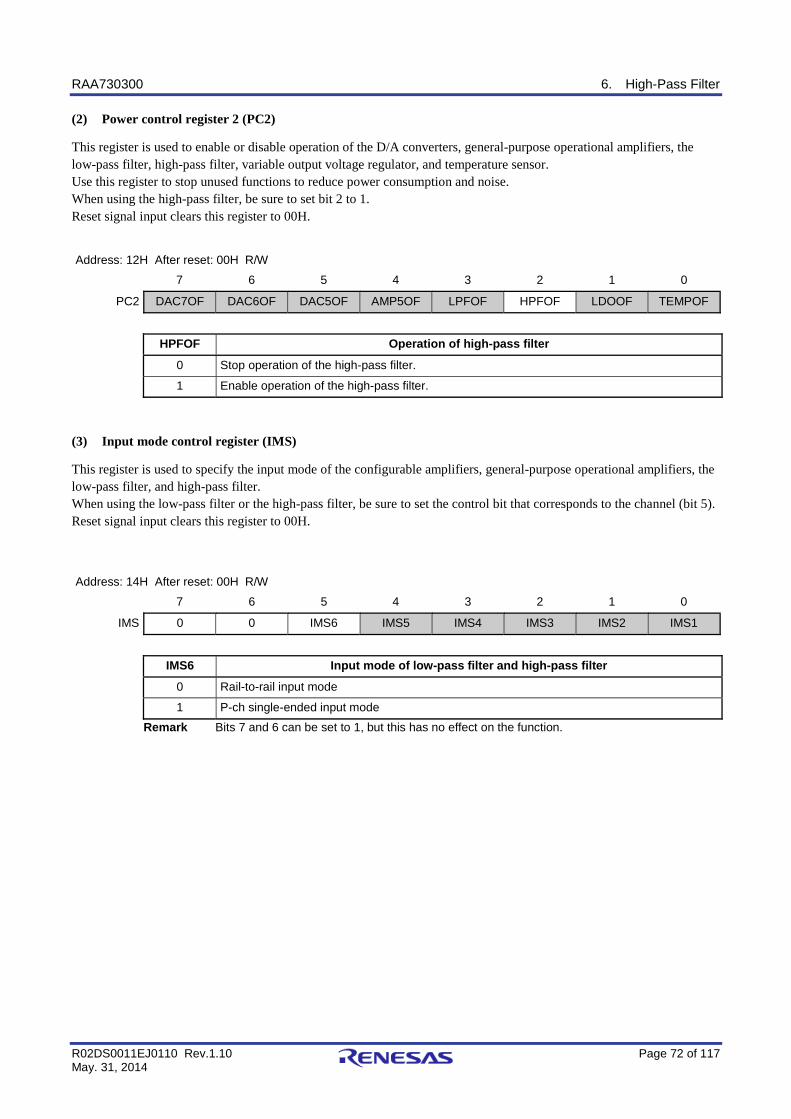
RAA730300 6. High-Pass Filter
R02DS0011EJ0110 Rev.1.10 Page 72 of 117 May. 31, 2014
(2) Power control register 2 (PC2)
This register is used to enable or disable operation of the D/A converters, general-purpose operational amplifiers, the low-pass filter, high-pass filter, variable output voltage regulator, and temperature sensor. Use this register to stop unused functions to reduce power consumption and noise. When using the high-pass filter, be sure to set bit 2 to 1. Reset signal input clears this register to 00H.
Address: 12H After reset: 00H R/W
7 6 5 4 3 2 1 0
PC2 DAC7OF DAC6OF DAC5OF AMP5OF LPFOF HPFOF LDOOF TEMPOF
HPFOF Operation of high-pass filter
0 Stop operation of the high-pass filter.
1 Enable operation of the high-pass filter.
(3) Input mode control register (IMS)
This register is used to specify the input mode of the configurable amplifiers, general-purpose operational amplifiers, the low-pass filter, and high-pass filter. When using the low-pass filter or the high-pass filter, be sure to set the control bit that corresponds to the channel (bit 5). Reset signal input clears this register to 00H.
Address: 14H After reset: 00H R/W
7 6 5 4 3 2 1 0
IMS 0 0 IMS6 IMS5 IMS4 IMS3 IMS2 IMS1
IMS6 Input mode of low-pass filter and high-pass filter
0 Rail-to-rail input mode
1 P-ch single-ended input mode
Remark Bits 7 and 6 can be set to 1, but this has no effect on the function.

RAA730300 6. High-Pass Filter
R02DS0011EJ0110 Rev.1.10 Page 73 of 117 May. 31, 2014
6.4 Procedure for Operating the High-Pass Filter
Follow the procedures below to start and stop the high-pass filter.
Example of procedure for starting the high-pass filter
Start
Set MPX3 registerSelect the signal processing route. (SCF0 = *)
Remark *: don't care
Set PC2 registerStart operation of the high-pass filter. (HPFOF = 1)
Operation starts
Input control clock to CLK_HPF pin
Set IMS register Specify the input mode. (IMS6 = *)
Example of procedure for stopping the high-pass filter
Operating
Set PC2 register
Operation stops
Stop operation of the high-pass filter. (HPFOF = 0)

RAA730300 7. Temperature Sensor
R02DS0011EJ0110 Rev.1.10 Page 74 of 117 May. 31, 2014
7. Temperature Sensor
The RAA730300 has one on-chip temperature sensor channel.
7.1 Overview of Temperature Sensor Features
The temperature sensor has the following features:
• Output voltage temperature coefficient: −4 mV/°C (Typ.)
• Includes a power-off function.
7.2 Block Diagram
+
-
AVDD2
TEMP_OUT
Internal bus
TEMPOF
AVDD2
AGND3
Power control register 2 (PC2)

RAA730300 7. Temperature Sensor
R02DS0011EJ0110 Rev.1.10 Page 75 of 117 May. 31, 2014
7.3 Registers Controlling the Temperature Sensor
The temperature sensor is controlled by power control register 2 (PC2).
(1) Power control register 2 (PC2)
This register is used to enable or disable operation of the D/A converters, general-purpose operational amplifiers, the low-pass filter, high-pass filter, variable output voltage regulator, and temperature sensor. Use this register to stop unused functions to reduce power consumption and noise. When selecting the signal to be input to the temperature sensor, be sure to set bit 0 to 1. Reset signal input clears this register to 00H.
Address: 12H After reset: 00H R/W
7 6 5 4 3 2 1 0
PC2 DAC7OF DAC6OF DAC5OF AMP5OF LPFOF HPFOF LDOOF TEMPOF
TEMPOF Operation of temperature sensor
0 Stop operation of the temperature sensor.
1 Enable operation of the temperature sensor.

RAA730300 7. Temperature Sensor
R02DS0011EJ0110 Rev.1.10 Page 76 of 117 May. 31, 2014
7.4 Procedure for Operating the Temperature Sensor
Follow the procedures below to start and stop the temperature sensor.
Example of procedure for starting the temperature sensor
Start
Set PC2 registerStart operation of the temperature sensor. (TEMPOF = 1)
Operation starts
Example of procedure for stopping the temperature sensor
Operating
Set PC2 register
Operation stops
Stop operation of the temperature sensor. (TEMPOF = 0)
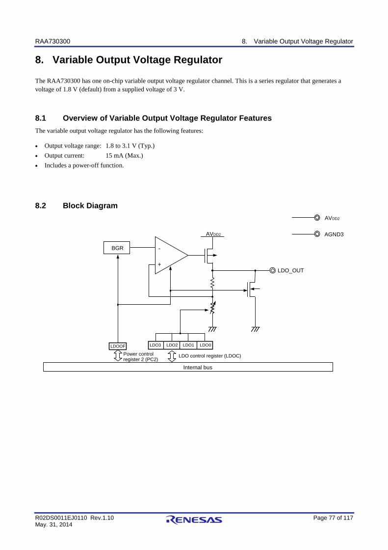
RAA730300 8. Variable Output Voltage Regulator
R02DS0011EJ0110 Rev.1.10 Page 77 of 117 May. 31, 2014
8. Variable Output Voltage Regulator
The RAA730300 has one on-chip variable output voltage regulator channel. This is a series regulator that generates a voltage of 1.8 V (default) from a supplied voltage of 3 V.
8.1 Overview of Variable Output Voltage Regulator Features
The variable output voltage regulator has the following features:
• Output voltage range: 1.8 to 3.1 V (Typ.)
• Output current: 15 mA (Max.)
• Includes a power-off function.
8.2 Block Diagram
AVDD2
+
-BGR
LDO_OUT
LDO2 LDO1LDO3
LDO control register (LDOC)
Internal bus
LDOOF
Power control register 2 (PC2)
AVDD2
AGND3
LDO0
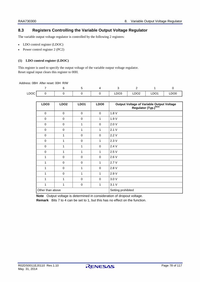
RAA730300 8. Variable Output Voltage Regulator
R02DS0011EJ0110 Rev.1.10 Page 78 of 117 May. 31, 2014
8.3 Registers Controlling the Variable Output Voltage Regulator
The variable output voltage regulator is controlled by the following 2 registers:
• LDO control register (LDOC)
• Power control register 2 (PC2)
(1) LDO control register (LDOC)
This register is used to specify the output voltage of the variable output voltage regulator. Reset signal input clears this register to 00H.
Address: 0BH After reset: 00H R/W
7 6 5 4 3 2 1 0
LDOC 0 0 0 0 LDO3 LDO2 LDO1 LDO0
LDO3 LDO2 LDO1 LDO0 Output Voltage of Variable Output Voltage Regulator (Typ.)Note
0 0 0 0 1.8 V
0 0 0 1 1.9 V
0 0 1 0 2.0 V
0 0 1 1 2.1 V
0 1 0 0 2.2 V
0 1 0 1 2.3 V
0 1 1 0 2.4 V
0 1 1 1 2.5 V
1 0 0 0 2.6 V
1 0 0 1 2.7 V
1 0 1 0 2.8 V
1 0 1 1 2.9 V
1 1 0 0 3.0 V
1 1 0 1 3.1 V
Other than above Setting prohibited
Note Output voltage is determined in consideration of dropout voltage. Remark Bits 7 to 4 can be set to 1, but this has no effect on the function.

RAA730300 8. Variable Output Voltage Regulator
R02DS0011EJ0110 Rev.1.10 Page 79 of 117 May. 31, 2014
(2) Power control register 2 (PC2)
This register is used to enable or disable operation of the D/A converters, general-purpose operational amplifiers, the low-pass filter, high-pass filter, variable output voltage regulator, and temperature sensor. Use this register to stop unused functions to reduce power consumption and noise. When using the variable output voltage regulator, be sure to set bit 1 to 1. Reset signal input clears this register to 00H.
Address: 12H After reset: 00H R/W
7 6 5 4 3 2 1 0
PC2 DAC7OF DAC6OF DAC5OF AMP5OF LPFOF HPFOF LDOOF TEMPOF
LDOOF Operation of variable output voltage regulator
0 Stop operation of the variable output voltage regulator.
1 Enable operation of the variable output voltage regulator.
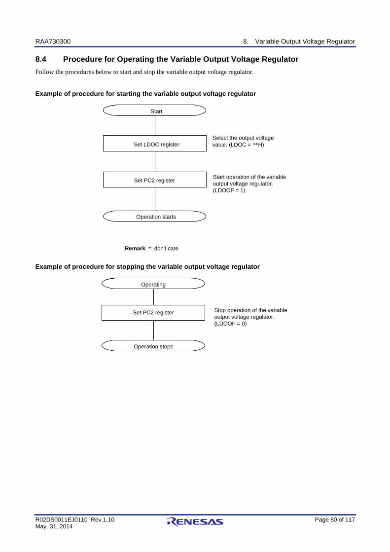
RAA730300 8. Variable Output Voltage Regulator
R02DS0011EJ0110 Rev.1.10 Page 80 of 117 May. 31, 2014
8.4 Procedure for Operating the Variable Output Voltage Regulator
Follow the procedures below to start and stop the variable output voltage regulator.
Example of procedure for starting the variable output voltage regulator
Start
Set LDOC registerSelect the output voltage value. (LDOC = **H)
Remark *: don't care
Set PC2 register Start operation of the variable output voltage regulator. (LDOOF = 1)
Operation starts
Example of procedure for stopping the variable output voltage regulator
Operating
Set PC2 register
Operation stops
Stop operation of the variable output voltage regulator. (LDOOF = 0)
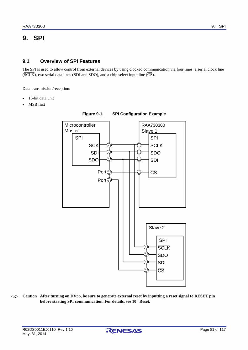
RAA730300 9. SPI
R02DS0011EJ0110 Rev.1.10 Page 81 of 117 May. 31, 2014
9. SPI
9.1 Overview of SPI Features
The SPI is used to allow control from external devices by using clocked communication via four lines: a serial clock line (SCLK), two serial data lines (SDI and SDO), and a chip select input line (CS).
Data transmission/reception:
• 16-bit data unit
• MSB first
Figure 9-1. SPI Configuration Example
MicrocontrollerMaster
SPISCKSDI
SDO
RAA730300Slave 1
SPISCLKSDOSDI
CS
Slave 2
SPISCLKSDOSDI
CS
Port
Port
Caution After turning on DVDD, be sure to generate external reset by inputting a reset signal to RESET pin before starting SPI communication. For details, see 10 Reset.
<R>
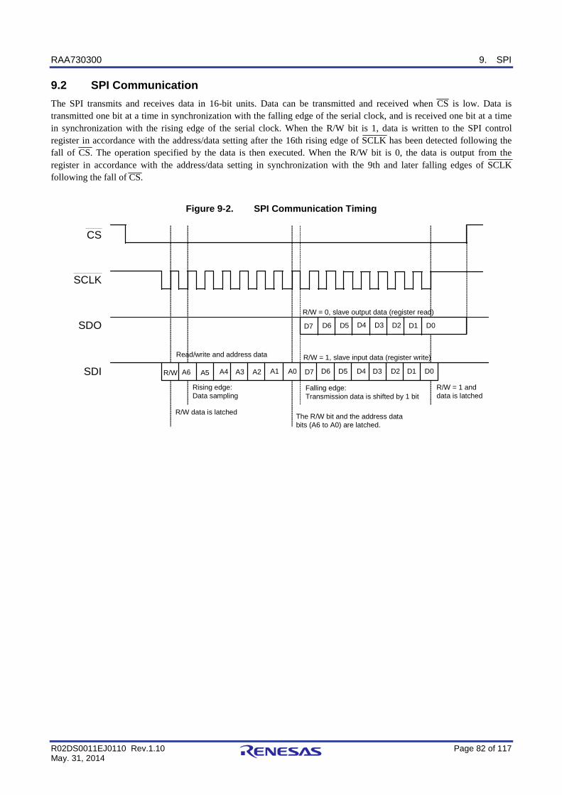
RAA730300 9. SPI
R02DS0011EJ0110 Rev.1.10 Page 82 of 117 May. 31, 2014
9.2 SPI Communication
The SPI transmits and receives data in 16-bit units. Data can be transmitted and received when CS is low. Data is transmitted one bit at a time in synchronization with the falling edge of the serial clock, and is received one bit at a time in synchronization with the rising edge of the serial clock. When the R/W bit is 1, data is written to the SPI control register in accordance with the address/data setting after the 16th rising edge of SCLK has been detected following the fall of CS. The operation specified by the data is then executed. When the R/W bit is 0, the data is output from the register in accordance with the address/data setting in synchronization with the 9th and later falling edges of SCLK following the fall of CS.
Figure 9-2. SPI Communication Timing
Read/write and address data
R/W = 0, slave output data (register read)
R/W = 1, slave input data (register write)
Rising edge: Data sampling
R/W = 1 and data is latched
Falling edge: Transmission data is shifted by 1 bit
The R/W bit and the address data bits (A6 to A0) are latched.
SDI
R/W data is latched
SCLK
CS
SDO D7 D6 D5 D4 D3 D2 D1 D0
R/W A6 A5 A4 A3 A2 A1 A0 D7 D6 D5 D4 D3 D2 D1 D0
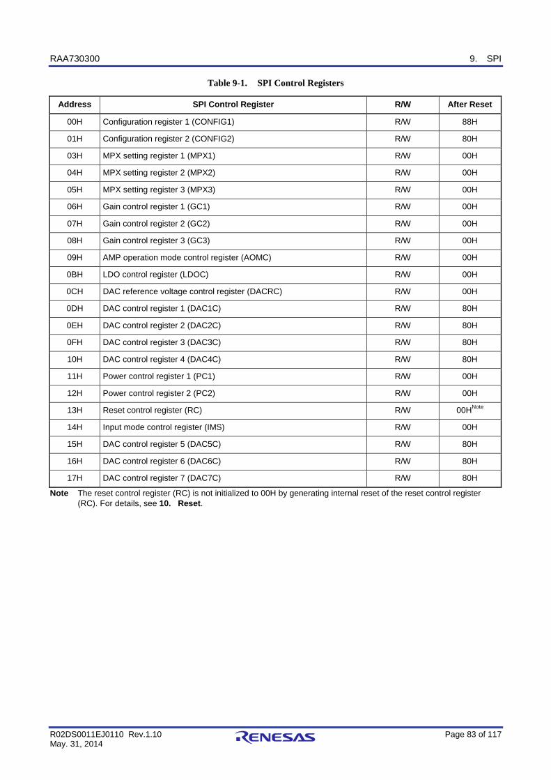
RAA730300 9. SPI
R02DS0011EJ0110 Rev.1.10 Page 83 of 117 May. 31, 2014
Table 9-1. SPI Control Registers
Address SPI Control Register R/W After Reset
00H Configuration register 1 (CONFIG1) R/W 88H
01H Configuration register 2 (CONFIG2) R/W 80H
03H MPX setting register 1 (MPX1) R/W 00H
04H MPX setting register 2 (MPX2) R/W 00H
05H MPX setting register 3 (MPX3) R/W 00H
06H Gain control register 1 (GC1) R/W 00H
07H Gain control register 2 (GC2) R/W 00H
08H Gain control register 3 (GC3) R/W 00H
09H AMP operation mode control register (AOMC) R/W 00H
0BH LDO control register (LDOC) R/W 00H
0CH DAC reference voltage control register (DACRC) R/W 00H
0DH DAC control register 1 (DAC1C) R/W 80H
0EH DAC control register 2 (DAC2C) R/W 80H
0FH DAC control register 3 (DAC3C) R/W 80H
10H DAC control register 4 (DAC4C) R/W 80H
11H Power control register 1 (PC1) R/W 00H
12H Power control register 2 (PC2) R/W 00H
13H Reset control register (RC) R/W 00HNote
14H Input mode control register (IMS) R/W 00H
15H DAC control register 5 (DAC5C) R/W 80H
16H DAC control register 6 (DAC6C) R/W 80H
17H DAC control register 7 (DAC7C) R/W 80H
Note The reset control register (RC) is not initialized to 00H by generating internal reset of the reset control register (RC). For details, see 10. Reset.
RAA730300 10. Reset
R02DS0011EJ0110 Rev.1.10 Page 84 of 117 May. 31, 2014
10. Reset
10.1 Overview of Reset Feature
The RAA730300 has an on-chip reset function. The SPI control registers are initialized by reset. A reset can be generated in the following two ways:
• External reset by inputting an external reset signal to the RESET pin
• Internal reset by writing 1 to the RESET bit of the reset control register (RC)
The functions of the external reset and the internal reset are described below.
• After turning on DVDD, be sure to generate external reset by inputting a reset signal to RESET pin before starting SPI communication.
• During reset, each function is shifted to the status shown in Table 10-1. The status of each SPI control register after reset has been acknowledged is shown in Table 10-2. After reset, the status of each pin is shown in Table 10-3.
• External reset is generated when a low-level signal is input to the RESET pin. On the other hand, internal reset is generated when 1 is written to the RESET bit of the reset control register (RC).
• External reset is subsequently cancelled by inputting a high-level signal to RESET pin after a low-level signal is input to this pin. On the other hand, internal reset is subsequently cancelled by writing 0 to the RESET bit of the reset control register (RC) after 1 is written to the same bit of this register.
Caution When generating an external reset, input a low-level signal to the RESET pin for at least 10 μs.
<R>
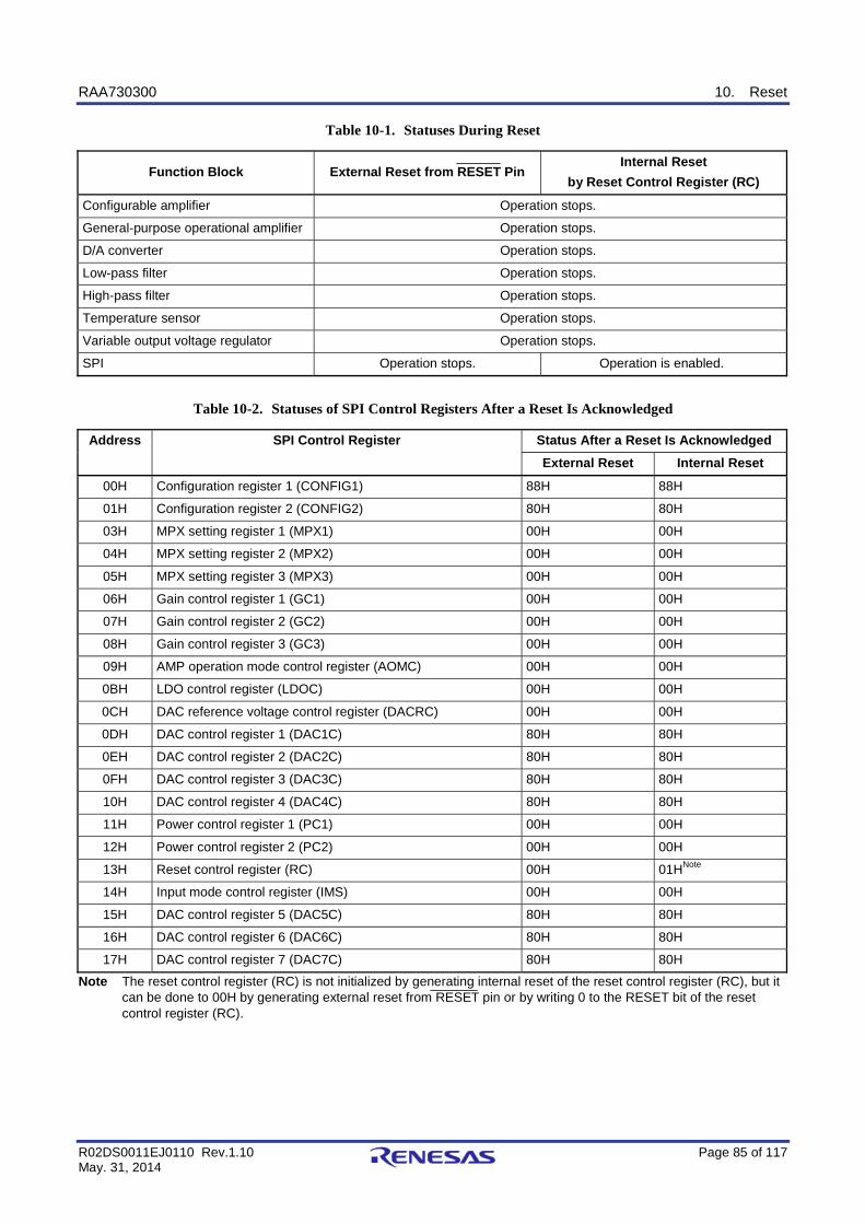
RAA730300 10. Reset
R02DS0011EJ0110 Rev.1.10 Page 85 of 117 May. 31, 2014
Table 10-1. Statuses During Reset
Function Block External Reset from RESET Pin Internal Reset
by Reset Control Register (RC)
Configurable amplifier Operation stops.
General-purpose operational amplifier Operation stops.
D/A converter Operation stops.
Low-pass filter Operation stops.
High-pass filter Operation stops.
Temperature sensor Operation stops.
Variable output voltage regulator Operation stops.
SPI Operation stops. Operation is enabled.
Table 10-2. Statuses of SPI Control Registers After a Reset Is Acknowledged
Address SPI Control Register Status After a Reset Is Acknowledged
External Reset Internal Reset
00H Configuration register 1 (CONFIG1) 88H 88H
01H Configuration register 2 (CONFIG2) 80H 80H
03H MPX setting register 1 (MPX1) 00H 00H
04H MPX setting register 2 (MPX2) 00H 00H
05H MPX setting register 3 (MPX3) 00H 00H
06H Gain control register 1 (GC1) 00H 00H
07H Gain control register 2 (GC2) 00H 00H
08H Gain control register 3 (GC3) 00H 00H
09H AMP operation mode control register (AOMC) 00H 00H
0BH LDO control register (LDOC) 00H 00H
0CH DAC reference voltage control register (DACRC) 00H 00H
0DH DAC control register 1 (DAC1C) 80H 80H
0EH DAC control register 2 (DAC2C) 80H 80H
0FH DAC control register 3 (DAC3C) 80H 80H
10H DAC control register 4 (DAC4C) 80H 80H
11H Power control register 1 (PC1) 00H 00H
12H Power control register 2 (PC2) 00H 00H
13H Reset control register (RC) 00H 01HNote
14H Input mode control register (IMS) 00H 00H
15H DAC control register 5 (DAC5C) 80H 80H
16H DAC control register 6 (DAC6C) 80H 80H
17H DAC control register 7 (DAC7C) 80H 80H
Note The reset control register (RC) is not initialized by generating internal reset of the reset control register (RC), but it can be done to 00H by generating external reset from RESET pin or by writing 0 to the RESET bit of the reset control register (RC).
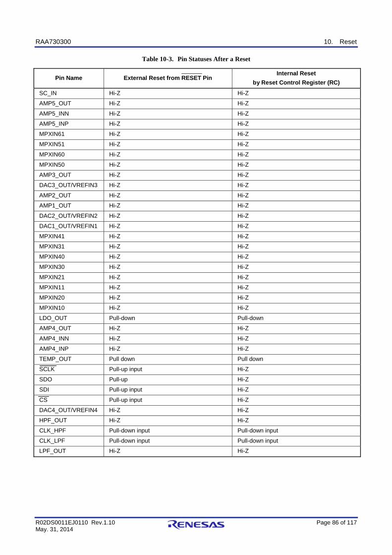
RAA730300 10. Reset
R02DS0011EJ0110 Rev.1.10 Page 86 of 117 May. 31, 2014
Table 10-3. Pin Statuses After a Reset
Pin Name External Reset from RESET Pin Internal Reset
by Reset Control Register (RC)
SC_IN Hi-Z Hi-Z
AMP5_OUT Hi-Z Hi-Z
AMP5_INN Hi-Z Hi-Z
AMP5_INP Hi-Z Hi-Z
MPXIN61 Hi-Z Hi-Z
MPXIN51 Hi-Z Hi-Z
MPXIN60 Hi-Z Hi-Z
MPXIN50 Hi-Z Hi-Z
AMP3_OUT Hi-Z Hi-Z
DAC3_OUT/VREFIN3 Hi-Z Hi-Z
AMP2_OUT Hi-Z Hi-Z
AMP1_OUT Hi-Z Hi-Z
DAC2_OUT/VREFIN2 Hi-Z Hi-Z
DAC1_OUT/VREFIN1 Hi-Z Hi-Z
MPXIN41 Hi-Z Hi-Z
MPXIN31 Hi-Z Hi-Z
MPXIN40 Hi-Z Hi-Z
MPXIN30 Hi-Z Hi-Z
MPXIN21 Hi-Z Hi-Z
MPXIN11 Hi-Z Hi-Z
MPXIN20 Hi-Z Hi-Z
MPXIN10 Hi-Z Hi-Z
LDO_OUT Pull-down Pull-down
AMP4_OUT Hi-Z Hi-Z
AMP4_INN Hi-Z Hi-Z
AMP4_INP Hi-Z Hi-Z
TEMP_OUT Pull down Pull down
SCLK Pull-up input Hi-Z
SDO Pull-up Hi-Z
SDI Pull-up input Hi-Z
CS Pull-up input Hi-Z
DAC4_OUT/VREFIN4 Hi-Z Hi-Z
HPF_OUT Hi-Z Hi-Z
CLK_HPF Pull-down input Pull-down input
CLK_LPF Pull-down input Pull-down input
LPF_OUT Hi-Z Hi-Z
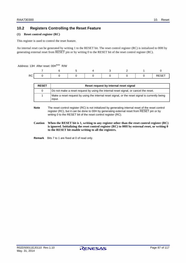
RAA730300 10. Reset
R02DS0011EJ0110 Rev.1.10 Page 87 of 117 May. 31, 2014
10.2 Registers Controlling the Reset Feature
(1) Reset control register (RC)
This register is used to control the reset feature.
An internal reset can be generated by writing 1 to the RESET bit. The reset control register (RC) is initialized to 00H by generating external reset from RESET pin or by writing 0 to the RESET bit of the reset control register (RC).
Address: 13H After reset: 00HNote R/W
7 6 5 4 3 2 1 0
RC 0 0 0 0 0 0 0 RESET
RESET Reset request by internal reset signal
0 Do not make a reset request by using the internal reset signal, or cancel the reset.
1 Make a reset request by using the internal reset signal, or the reset signal is currently being input.
Note The reset control register (RC) is not initialized by generating internal reset of the reset control
register (RC), but it can be done to 00H by generating external reset from RESET pin or by writing 0 to the RESET bit of the reset control register (RC).
Caution When the RESET bit is 1, writing to any register other than the reset control register (RC)
is ignored. Initializing the reset control register (RC) to 00H by external reset, or writing 0 to the RESET bit enable writing to all the registers.
Remark Bits 7 to 1 are fixed at 0 of read only.
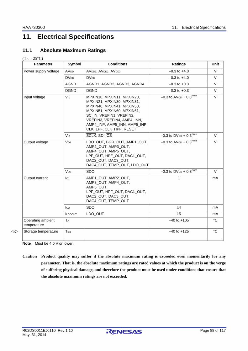
RAA730300 11. Electrical Specifications
R02DS0011EJ0110 Rev.1.10 Page 88 of 117 May. 31, 2014
11. Electrical Specifications
11.1 Absolute Maximum Ratings
(TA = 25°C) Parameter Symbol Conditions Ratings Unit
Power supply voltage AVDD AVDD1, AVDD2, AVDD3 −0.3 to +4.0 V
DVDD DVDD −0.3 to +4.0 V
AGND AGND1, AGND2, AGND3, AGND4 −0.3 to +0.3 V
DGND DGND −0.3 to +0.3 V
Input voltage VI1 MPXIN10, MPXIN11, MPXIN20, MPXIN21, MPXIN30, MPXIN31, MPXIN40, MPXIN41, MPXIN50, MPXIN51, MPXIN60, MPXIN61, SC_IN, VREFIN1, VREFIN2, VREFIN3, VREFIN4, AMP4_INN, AMP4_INP, AMP5_INN, AMP5_INP, CLK_LPF, CLK_HPF, RESET
−0.3 to AVDD + 0.3Note V
VI2 SCLK, SDI, CS −0.3 to DVDD + 0.3Note V
Output voltage VO1 LDO_OUT, BGR_OUT, AMP1_OUT, AMP2_OUT, AMP3_OUT, AMP4_OUT, AMP5_OUT, LPF_OUT, HPF_OUT, DAC1_OUT, DAC2_OUT, DAC3_OUT, DAC4_OUT, TEMP_OUT, LDO_OUT
−0.3 to AVDD + 0.3Note V
VO2 SDO −0.3 to DVDD + 0.3Note V
Output current IO1 AMP1_OUT, AMP2_OUT, AMP3_OUT, AMP4_OUT, AMP5_OUT, LPF_OUT, HPF_OUT, DAC1_OUT, DAC2_OUT, DAC3_OUT, DAC4_OUT, TEMP_OUT
1 mA
IO2 SDO ±4 mA
ILDOOUT LDO_OUT 15 mA
Operating ambient temperature
TA −40 to +105 °C
Storage temperature
Tstg −40 to +125 °C
Note Must be 4.0 V or lower.
Caution Product quality may suffer if the absolute maximum rating is exceeded even momentarily for any parameter. That is, the absolute maximum ratings are rated values at which the product is on the verge of suffering physical damage, and therefore the product must be used under conditions that ensure that the absolute maximum ratings are not exceeded.
<R>
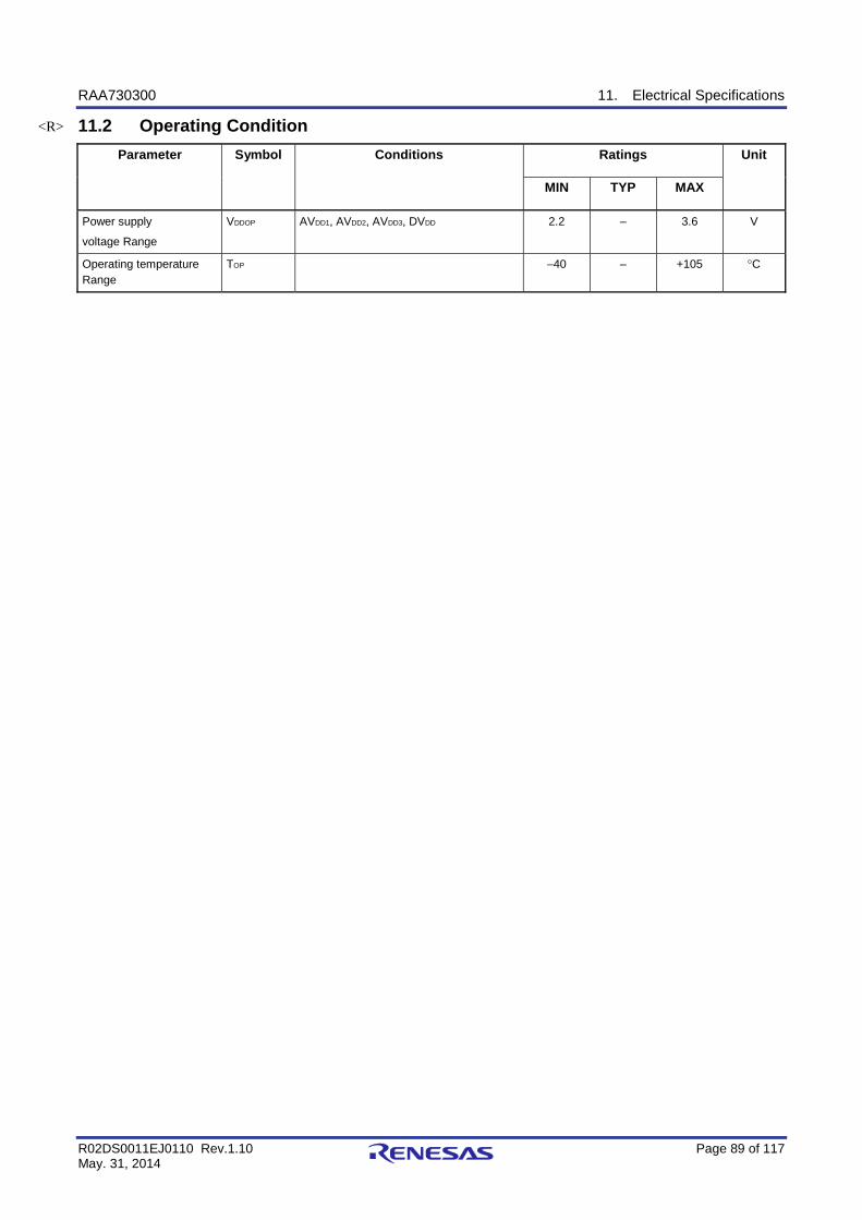
RAA730300 11. Electrical Specifications
R02DS0011EJ0110 Rev.1.10 Page 89 of 117 May. 31, 2014
11.2 Operating Condition
Parameter Symbol Conditions Ratings Unit
MIN TYP MAX
Power supply
voltage Range
VDDOP AVDD1, AVDD2, AVDD3, DVDD 2.2 – 3.6 V
Operating temperature Range
TOP −40 – +105 °C
<R>
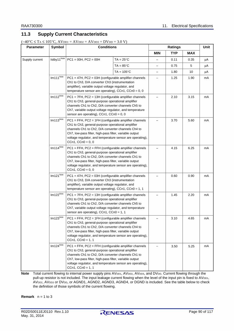
RAA730300 11. Electrical Specifications
R02DS0011EJ0110 Rev.1.10 Page 90 of 117 May. 31, 2014
11.3 Supply Current Characteristics
(−40°C ≤ TA ≤ 105°C, AVDD1 = AVDD2 = AVDD3 = DVDD = 3.0 V) Parameter Symbol Conditions Ratings Unit
MIN TYP MAX
Supply current Istby11Note PC1 = 00H, PC2 = 00H TA = 25°C – 0.11 0.35 μA
TA = 85°C – 0.75 5 μA
TA = 105°C – 1.80 10 μA
Im111Note PC1 = 47H, PC2 = 03H (configurable amplifier channels Ch1 to Ch3, D/A converter Ch3 (instrumentation amplifier), variable output voltage regulator, and temperature sensor are operating), CCn1, CCn0 = 0, 0
– 1.25 1.90 mA
Im112Note PC1 = 7FH, PC2 = 13H (configurable amplifier channels Ch1 to Ch3, general-purpose operational amplifier channels Ch1 to Ch2, D/A converter channels Ch5 to Ch7, variable output voltage regulator, and temperature sensor are operating), CCn1, CCn0 = 0, 0
– 2.10 3.15 mA
Im113Note PC1 = FFH, PC2 = 1FH (configurable amplifier channels Ch1 to Ch3, general-purpose operational amplifier channels Ch1 to Ch2, D/A converter channels Ch4 to Ch7, low-pass filter, high-pass filter, variable output voltage regulator, and temperature sensor are operating), CCn1, CCn0 = 0, 0
– 3.70 5.60 mA
Im114Note PC1 = FFH, PC2 = FFH (configurable amplifier channels Ch1 to Ch3, general-purpose operational amplifier channels Ch1 to Ch2, D/A converter channels Ch1 to Ch7, low-pass filter, high-pass filter, variable output voltage regulator, and temperature sensor are operating), CCn1, CCn0 = 0, 0
– 4.15 6.25 mA
Im121Note PC1 = 47H, PC2 = 03H (configurable amplifier channels Ch1 to Ch3, D/A converter Ch3 (instrumentation amplifier), variable output voltage regulator, and temperature sensor are operating), CCn1, CCn0 = 1, 1
– 0.60 0.90 mA
Im122Note PC1 = 7FH, PC2 = 13H (configurable amplifier channels Ch1 to Ch3, general-purpose operational amplifier channels Ch1 to Ch2, D/A converter channels Ch5 to Ch7, variable output voltage regulator, and temperature sensor are operating), CCn1, CCn0 = 1, 1
– 1.45 2.20 mA
Im123Note PC1 = FFH, PC2 = 1FH (configurable amplifier channels Ch1 to Ch3, general-purpose operational amplifier channels Ch1 to Ch2, D/A converter channels Ch4 to Ch7, low-pass filter, high-pass filter, variable output voltage regulator, and temperature sensor are operating), CCn1, CCn0 = 1, 1
– 3.10 4.65 mA
Im124Note PC1 = FFH, PC2 = FFH (configurable amplifier channels Ch1 to Ch3, general-purpose operational amplifier channels Ch1 to Ch2, D/A converter channels Ch1 to Ch7, low-pass filter, high-pass filter, variable output voltage regulator, and temperature sensor are operating), CCn1, CCn0 = 1, 1
– 3.50 5.25 mA
Note Total current flowing to internal power supply pins AVDD1, AVDD2, AVDD3, and DVDD. Current flowing through the pull-up resistor is not included. The input leakage current flowing when the level of the input pin is fixed to AVDD1, AVDD2, AVDD3 or DVDD, or AGND1, AGND2, AGND3, AGND4, or DGND is included. See the table below to check the definition of those symbols of the current flowing.
Remark n = 1 to 3
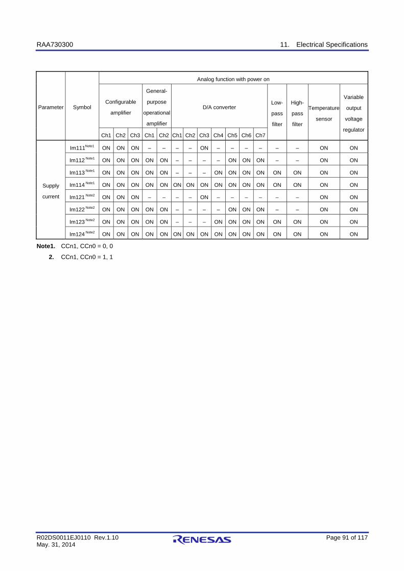
RAA730300 11. Electrical Specifications
R02DS0011EJ0110 Rev.1.10 Page 91 of 117 May. 31, 2014
Note1. CCn1, CCn0 = 0, 0
2. CCn1, CCn0 = 1, 1
Parameter Symbol
Analog function with power on
Configurable
amplifier
General-
purpose
operational
amplifier
D/A converter Low-
pass
filter
High-
pass
filter
Temperature
sensor
Variable
output
voltage
regulatorCh1 Ch2 Ch3 Ch1 Ch2 Ch1 Ch2 Ch3 Ch4 Ch5 Ch6 Ch7
Supply
current
Im111Note1 ON ON ON – – – – ON – – – – – – ON ON
Im112 Note1 ON ON ON ON ON – – – – ON ON ON – – ON ON
Im113 Note1 ON ON ON ON ON – – – ON ON ON ON ON ON ON ON
Im114 Note1 ON ON ON ON ON ON ON ON ON ON ON ON ON ON ON ON
Im121 Note2 ON ON ON – – – – ON – – – – – – ON ON
Im122 Note2 ON ON ON ON ON – – – – ON ON ON – – ON ON
Im123 Note2 ON ON ON ON ON – – – ON ON ON ON ON ON ON ON
Im124 Note2 ON ON ON ON ON ON ON ON ON ON ON ON ON ON ON ON

RAA730300 11. Electrical Specifications
R02DS0011EJ0110 Rev.1.10 Page 92 of 117 May. 31, 2014
11.4 Electrical Specifications of Each Block
(1) Configurable amplifier block characteristics
(−40°C ≤ TA ≤ 105°C, AVDD1 = AVDD2 = AVDD3 = DVDD = 3.0 V, VREFIN1 = VREFIN2 = VREFIN3 = 1.5 V, AMP1OF = AMP2OF = AMP3OF = 1, DAC1OF = DAC2OF = DAC3OF = 0, non-inverting amplifier)
Parameter Symbol Conditions Ratings Unit
MIN TYP MAX
Current consumption Note
Icc00 CCn1, CCn0 = 0, 0 – 330 500 μA
Icc01 CCn1, CCn0 = 0, 1 – 250 380 μA
Icc10 CCn1, CCn0 = 1, 0 – 170 260 μA
Icc11 CCn1, CCn0 = 1, 1 – 90 150 μA
Input voltage 1 VINL1 IMSn = 0 AGND1 – 0.05 – – V
VINH1 IMSn = 0 – – AVDD1 + 0.1 V
Input voltage 2 VINL2 IMSn = 1 AGND1 – 0.05 – – V
VINH2 IMSn = 1 – – AVDD1 – 1.4 V
Output voltage VOUTL IOL = –200 μA – – AGND1 + 0.1 V
VOUTH IOH = 200 μA AVDD1 – 0.1 – – V
Settling time tSET_AMP00 GCn = 00H (9.5 dB), CCn1, CCn0 = 0, 0, CL = 30 pF, output voltage = 1VPP, output convergence voltage VPP = 999 mV
– – 8 μs
tSET_AMP01 GCn = 00H (9.5 dB), CCn1, CCn0 = 0, 1, CL = 30 pF, output voltage = 1VPP, output convergence voltage VPP = 999 mV
– – 10 μs
tSET_AMP10 GCn = 00H (9.5 dB), CCn1, CCn0 = 1, 0, CL = 30 pF, output voltage = 1VPP, output convergence voltage VPP = 999 mV
– – 16 μs
tSET_AMP11 GCn = 00H (9.5 dB), CCn1, CCn0 = 1, 1, CL = 30 pF, output voltage = 1VPP, output convergence voltage VPP = 999 mV
– – 42 μs
Gain bandwidth GBW00 CLMAX = 30 pF, CCn1, CCn0 = 0, 0
GCn = 11H (40.1 dB)
– 1.35 – MHz
GBW01 CLMAX = 30 pF, CCn1, CCn0 = 0, 1
GCn = 11H (40.1 dB)
– 1.1 – MHz
GBW10 CLMAX = 30 pF, CCn1, CCn0 = 1, 0
GCn = 11H (40.1 dB)
– 0.75 – MHz
GBW11 CLMAX = 30 pF, CCn1, CC0 = 1, 1
GCn = 11H (40.1 dB)
– 0.4 – MHz
Equivalent input noise
En00 CCn1, CCn0 = 0, 0
f = 1 kHz, GCn = 11H (40.1 dB)
– 67 – nV/√ Hz
En01 CCn1, CCn0 = 0, 1 f = 1 kHz, GCn = 11H (40.1 dB)
– 75 – nV/√ Hz
En10 CCn1, CCn0 = 1, 0 f = 1 kHz, GCn = 11H (40.1 dB)
– 110 – nV/√ Hz
En11 CCn1, CCn0 = 1, 1 f = 1 kHz, GCn = 11H (40.1 dB)
– 145 – nV/√ Hz
Note These are the values for one channel of configurable amplifier. Remark n = 1 to 3
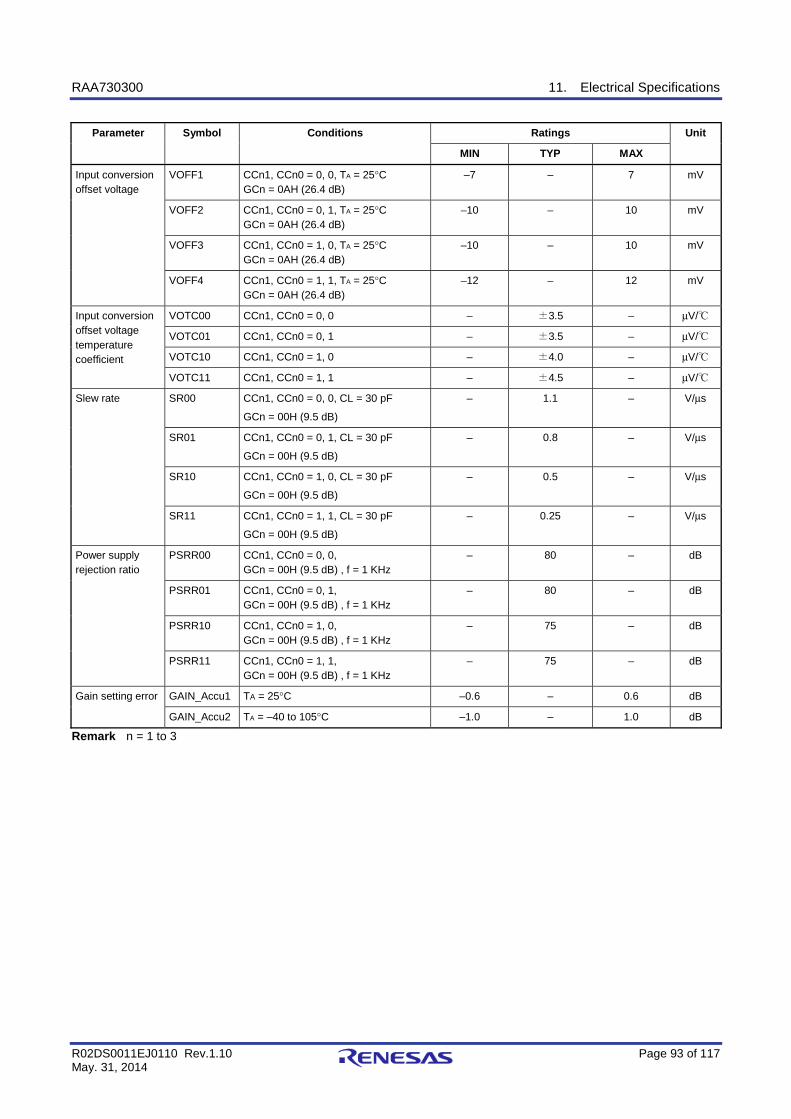
RAA730300 11. Electrical Specifications
R02DS0011EJ0110 Rev.1.10 Page 93 of 117 May. 31, 2014
Parameter Symbol Conditions Ratings Unit
MIN TYP MAX
Input conversion offset voltage
VOFF1 CCn1, CCn0 = 0, 0, TA = 25°C GCn = 0AH (26.4 dB)
–7 – 7 mV
VOFF2 CCn1, CCn0 = 0, 1, TA = 25°C GCn = 0AH (26.4 dB)
–10 – 10 mV
VOFF3 CCn1, CCn0 = 1, 0, TA = 25°C GCn = 0AH (26.4 dB)
–10 – 10 mV
VOFF4 CCn1, CCn0 = 1, 1, TA = 25°C GCn = 0AH (26.4 dB)
–12 – 12 mV
Input conversion offset voltage temperature coefficient
VOTC00 CCn1, CCn0 = 0, 0 – ±3.5 – μV/℃
VOTC01 CCn1, CCn0 = 0, 1 – ±3.5 – μV/℃
VOTC10 CCn1, CCn0 = 1, 0 – ±4.0 – μV/℃
VOTC11 CCn1, CCn0 = 1, 1 – ±4.5 – μV/℃
Slew rate SR00 CCn1, CCn0 = 0, 0, CL = 30 pF
GCn = 00H (9.5 dB)
– 1.1 – V/μs
SR01 CCn1, CCn0 = 0, 1, CL = 30 pF
GCn = 00H (9.5 dB)
– 0.8 – V/μs
SR10 CCn1, CCn0 = 1, 0, CL = 30 pF
GCn = 00H (9.5 dB)
– 0.5 – V/μs
SR11 CCn1, CCn0 = 1, 1, CL = 30 pF
GCn = 00H (9.5 dB)
– 0.25 – V/μs
Power supply rejection ratio
PSRR00 CCn1, CCn0 = 0, 0, GCn = 00H (9.5 dB) , f = 1 KHz
– 80 – dB
PSRR01 CCn1, CCn0 = 0, 1, GCn = 00H (9.5 dB) , f = 1 KHz
– 80 – dB
PSRR10 CCn1, CCn0 = 1, 0, GCn = 00H (9.5 dB) , f = 1 KHz
– 75 – dB
PSRR11 CCn1, CCn0 = 1, 1, GCn = 00H (9.5 dB) , f = 1 KHz
– 75 – dB
Gain setting error GAIN_Accu1 TA = 25°C –0.6 – 0.6 dB
GAIN_Accu2 TA = –40 to 105°C –1.0 – 1.0 dB
Remark n = 1 to 3
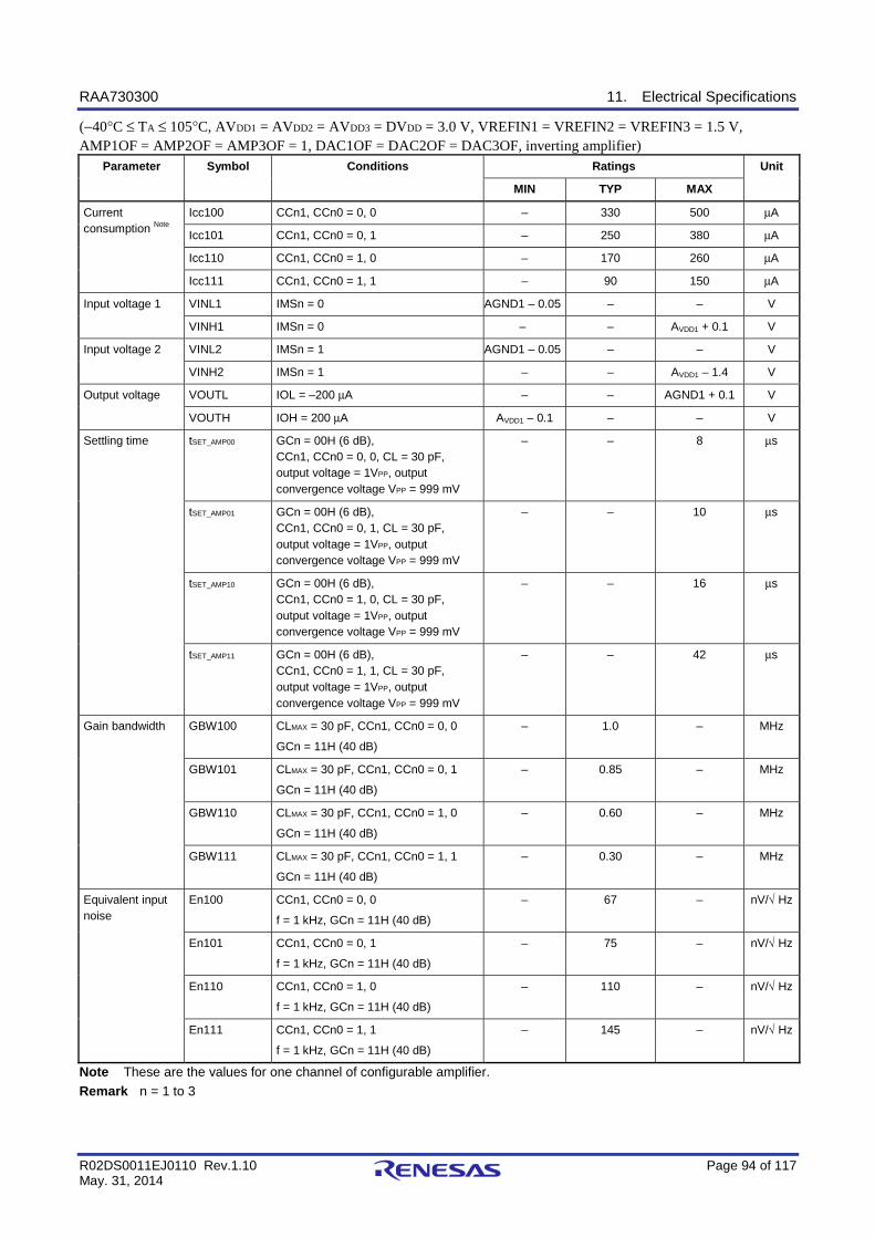
RAA730300 11. Electrical Specifications
R02DS0011EJ0110 Rev.1.10 Page 94 of 117 May. 31, 2014
(−40°C ≤ TA ≤ 105°C, AVDD1 = AVDD2 = AVDD3 = DVDD = 3.0 V, VREFIN1 = VREFIN2 = VREFIN3 = 1.5 V, AMP1OF = AMP2OF = AMP3OF = 1, DAC1OF = DAC2OF = DAC3OF, inverting amplifier)
Parameter Symbol Conditions Ratings Unit
MIN TYP MAX
Current consumption Note
Icc100 CCn1, CCn0 = 0, 0 – 330 500 μA
Icc101 CCn1, CCn0 = 0, 1 – 250 380 μA
Icc110 CCn1, CCn0 = 1, 0 – 170 260 μA
Icc111 CCn1, CCn0 = 1, 1 – 90 150 μA
Input voltage 1 VINL1 IMSn = 0 AGND1 – 0.05 – – V
VINH1 IMSn = 0 – – AVDD1 + 0.1 V
Input voltage 2 VINL2 IMSn = 1 AGND1 – 0.05 – – V
VINH2 IMSn = 1 – – AVDD1 – 1.4 V
Output voltage VOUTL IOL = –200 μA – – AGND1 + 0.1 V
VOUTH IOH = 200 μA AVDD1 – 0.1 – – V
Settling time tSET_AMP00 GCn = 00H (6 dB), CCn1, CCn0 = 0, 0, CL = 30 pF, output voltage = 1VPP, output convergence voltage VPP = 999 mV
– – 8 μs
tSET_AMP01 GCn = 00H (6 dB), CCn1, CCn0 = 0, 1, CL = 30 pF, output voltage = 1VPP, output convergence voltage VPP = 999 mV
– – 10 μs
tSET_AMP10 GCn = 00H (6 dB), CCn1, CCn0 = 1, 0, CL = 30 pF, output voltage = 1VPP, output convergence voltage VPP = 999 mV
– – 16 μs
tSET_AMP11 GCn = 00H (6 dB), CCn1, CCn0 = 1, 1, CL = 30 pF, output voltage = 1VPP, output convergence voltage VPP = 999 mV
– – 42 μs
Gain bandwidth GBW100 CLMAX = 30 pF, CCn1, CCn0 = 0, 0
GCn = 11H (40 dB)
– 1.0 – MHz
GBW101 CLMAX = 30 pF, CCn1, CCn0 = 0, 1
GCn = 11H (40 dB)
– 0.85 – MHz
GBW110 CLMAX = 30 pF, CCn1, CCn0 = 1, 0
GCn = 11H (40 dB)
– 0.60 – MHz
GBW111 CLMAX = 30 pF, CCn1, CCn0 = 1, 1
GCn = 11H (40 dB)
– 0.30 – MHz
Equivalent input noise
En100 CCn1, CCn0 = 0, 0
f = 1 kHz, GCn = 11H (40 dB)
– 67 – nV/√ Hz
En101 CCn1, CCn0 = 0, 1
f = 1 kHz, GCn = 11H (40 dB)
– 75 – nV/√ Hz
En110 CCn1, CCn0 = 1, 0
f = 1 kHz, GCn = 11H (40 dB)
– 110 – nV/√ Hz
En111 CCn1, CCn0 = 1, 1
f = 1 kHz, GCn = 11H (40 dB)
– 145 – nV/√ Hz
Note These are the values for one channel of configurable amplifier. Remark n = 1 to 3

RAA730300 11. Electrical Specifications
R02DS0011EJ0110 Rev.1.10 Page 95 of 117 May. 31, 2014
Parameter Symbol Conditions Ratings Unit
MIN TYP MAX
Input conversion offset voltage
VOFF1 CCn1, CCn0 = 0, 0, TA = 25°C GCn = 0AH (26 dB)
–7 – 7 mV
VOFF2 CCn1, CCn0 = 0, 1, TA = 25°C GCn = 0AH (26 dB)
–10 – 10 mV
VOFF3 CCn1, CCn0 = 1, 0, TA = 25°C GCn = 0AH (26 dB)
–10 – 10 mV
VOFF4 CCn1, CCn0 = 1, 1, TA = 25°C GCn = 0AH (26 dB)
–12 – 12 mV
Input conversion offset voltage temperature coefficient
VOTC00 CCn1, CCn0 = 0, 0 – ±3.5 – μV/℃
VOTC01 CCn1, CCn0 = 0, 1 – ±3.5 – μV/℃
VOTC10 CCn1, CCn0 = 1, 0 – ±4.0 – μV/℃
VOTC11 CCn1, CCn0 = 1, 1 – ±4.5 – μV/℃
Slew rate SR100 CCn1, CCn0 = 0, 0, CL = 30 pF
GCn = 00H (6 dB)
– 1.2 – V/μs
SR101 CCn1, CCn0 = 0, 1, CL = 30 pF
GCn = 00H (6 dB)
– 0.9 – V/μs
SR110 CCn1, CCn0 = 1, 0, CL = 30 pF
GCn = 00H (6 dB)
– 0.6 – V/μs
SR111 CCn1, CCn0 = 1, 1, CL = 30 pF
GCn = 00H (6 dB)
– 0.3 – V/μs
Power supply rejection ratio
PSRR100 CCn1, CCn0 = 0, 0, GCn = 00H (6 dB), f = 1 kHz
– 80 – dB
PSRR101 CCn1, CCn0 = 0, 1, GCn = 00H (6 dB) , f = 1 kHz
– 80 – dB
PSRR110 CCn1, CCn0 = 1, 0, GCn = 00H (6 dB) , f = 1 kHz
– 80 – dB
PSRR111 CCn1, CCn0 = 1, 1, GCn = 00H (6 dB) , f = 1 kHz
– 80 – dB
Gain setting error GAIN_Accu1 TA = 25°C –0.6 – 0.6 dB
GAIN_Accu2 TA = –40 to 105°C –1.0 – 1.0 dB
Remark n = 1 to 3

RAA730300 11. Electrical Specifications
R02DS0011EJ0110 Rev.1.10 Page 96 of 117 May. 31, 2014
(−40°C ≤ TA ≤ 105°C, AVDD1 = AVDD2 = AVDD3 = DVDD = 3.0 V, VREFIN = VREFIN2 = VREFIN3 = 1.5 V, AMP1OF = AMP2OF = AMP3OF = 1, DAC1OF = DAC2OF = DAC3OF = 0, differential amplifier)
Parameter Symbol Conditions Ratings Unit
MIN TYP MAX
Current consumption Note
Icc00 CCn1, CCn0 = 0, 0 – 330 500 μA
Icc01 CCn1, CCn0 = 0, 1 – 250 380 μA
Icc10 CCn1, CCn0 = 1, 0 – 170 260 μA
Icc11 CCn1, CCn0 = 1, 1 – 90 150 μA
Input voltage 1 VINL1 IMSn = 0 AGND1 – 0.05 – – V
VINH1 IMSn = 0 – – AVDD1 + 0.1 V
Input voltage 2 VINL2 IMSn = 1 AGND1 – 0.05 – – V
VINH2 IMSn = 1 – – AVDD1 – 1.4 V
Output voltage VOUTL IOL = –200 μA – – AGND1 + 0.1 V
VOUTH IOH = 200 μA AVDD1 – 0.1 – – V
Settling time tSET_AMP00 GCn = 00H (6 dB), CCn1, CCn0 = 0, 0, CL = 30 pF, output voltage = 1VPP, output convergence voltage VPP = 999 mV
– – 8 μs
tSET_AMP01 GCn = 00H (6 dB), CCn1, CCn0 = 0, 1, CL = 30 pF, output voltage = 1VPP, output convergence voltage VPP = 999 mV
– – 10 μs
tSET_AMP10 GCn = 00H (6 dB), CCn1, CCn0 = 1, 0, CL = 30 pF, output voltage = 1VPP, output convergence voltage VPP = 999 mV
– – 16 μs
tSET_AMP11 GCn = 00H (6 dB), CCn1, CCn0 = 1, 1, CL = 30 pF, output voltage = 1VPP, output convergence voltage VPP = 999 mV
– – 42 μs
Gain bandwidth GBW00 CLMAX = 30 pF, CCn1, CCn0 = 0, 0
GCn = 11H (40 dB)
– 1.0 – MHz
GBW01 CLMAX = 30 pF, CCn1, CCn0 = 0, 1
GCn = 11H (40 dB)
– 0.85 – MHz
GBW10 CLMAX = 30 pF, CCn1, CCn0 = 1, 0
GCn = 11H (40 dB)
– 0.60 – MHz
GBW11 CLMAX = 30 pF, CCn1, CCn0 = 1, 1
GCn = 11H (40 dB)
– 0.30 – MHz
Equivalent input noise
En00 CCn1, CCn0 = 0, 0 f = 1 kHz, GCn = 11H (40 dB)
– 67 – nV/√ Hz
En01 CCn1, CCn0 = 0, 1 f = 1 kHz, GCn = 11H (40 dB)
– 75 – nV/√ Hz
En10 CCn1, CCn0 = 1, 0 f = 1 kHz, GCn = 11H (40 dB)
– 110 – nV/√ Hz
En11 CCn1, CCn0 = 1, 1 f = 1 kHz, GCn = 11H (40 dB)
– 145 – nV/√ Hz
Note These are the values for one channel of configurable amplifier. Remark n = 1 to 3
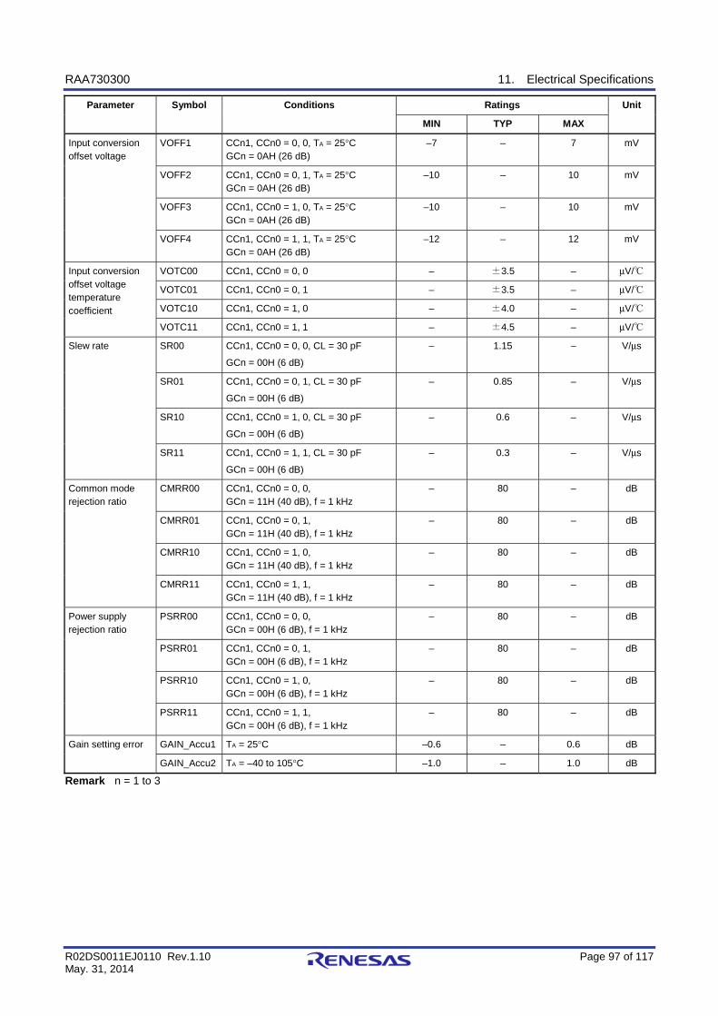
RAA730300 11. Electrical Specifications
R02DS0011EJ0110 Rev.1.10 Page 97 of 117 May. 31, 2014
Parameter Symbol Conditions Ratings Unit
MIN TYP MAX
Input conversion offset voltage
VOFF1 CCn1, CCn0 = 0, 0, TA = 25°C GCn = 0AH (26 dB)
–7 – 7 mV
VOFF2 CCn1, CCn0 = 0, 1, TA = 25°C GCn = 0AH (26 dB)
–10 – 10 mV
VOFF3 CCn1, CCn0 = 1, 0, TA = 25°C GCn = 0AH (26 dB)
–10 – 10 mV
VOFF4 CCn1, CCn0 = 1, 1, TA = 25°C GCn = 0AH (26 dB)
–12 – 12 mV
Input conversion offset voltage temperature coefficient
VOTC00 CCn1, CCn0 = 0, 0 – ±3.5 – μV/℃
VOTC01 CCn1, CCn0 = 0, 1 – ±3.5 – μV/℃
VOTC10 CCn1, CCn0 = 1, 0 – ±4.0 – μV/℃
VOTC11 CCn1, CCn0 = 1, 1 – ±4.5 – μV/℃
Slew rate SR00 CCn1, CCn0 = 0, 0, CL = 30 pF
GCn = 00H (6 dB)
– 1.15 – V/μs
SR01 CCn1, CCn0 = 0, 1, CL = 30 pF
GCn = 00H (6 dB)
– 0.85 – V/μs
SR10 CCn1, CCn0 = 1, 0, CL = 30 pF
GCn = 00H (6 dB)
– 0.6 – V/μs
SR11 CCn1, CCn0 = 1, 1, CL = 30 pF
GCn = 00H (6 dB)
– 0.3 – V/μs
Common mode rejection ratio
CMRR00 CCn1, CCn0 = 0, 0, GCn = 11H (40 dB), f = 1 kHz
– 80 – dB
CMRR01 CCn1, CCn0 = 0, 1, GCn = 11H (40 dB), f = 1 kHz
– 80 – dB
CMRR10 CCn1, CCn0 = 1, 0, GCn = 11H (40 dB), f = 1 kHz
– 80 – dB
CMRR11 CCn1, CCn0 = 1, 1, GCn = 11H (40 dB), f = 1 kHz
– 80 – dB
Power supply rejection ratio
PSRR00 CCn1, CCn0 = 0, 0, GCn = 00H (6 dB), f = 1 kHz
– 80 – dB
PSRR01 CCn1, CCn0 = 0, 1, GCn = 00H (6 dB), f = 1 kHz
– 80 – dB
PSRR10 CCn1, CCn0 = 1, 0, GCn = 00H (6 dB), f = 1 kHz
– 80 – dB
PSRR11 CCn1, CCn0 = 1, 1, GCn = 00H (6 dB), f = 1 kHz
– 80 – dB
Gain setting error GAIN_Accu1 TA = 25°C –0.6 – 0.6 dB
GAIN_Accu2 TA = –40 to 105°C –1.0 – 1.0 dB
Remark n = 1 to 3
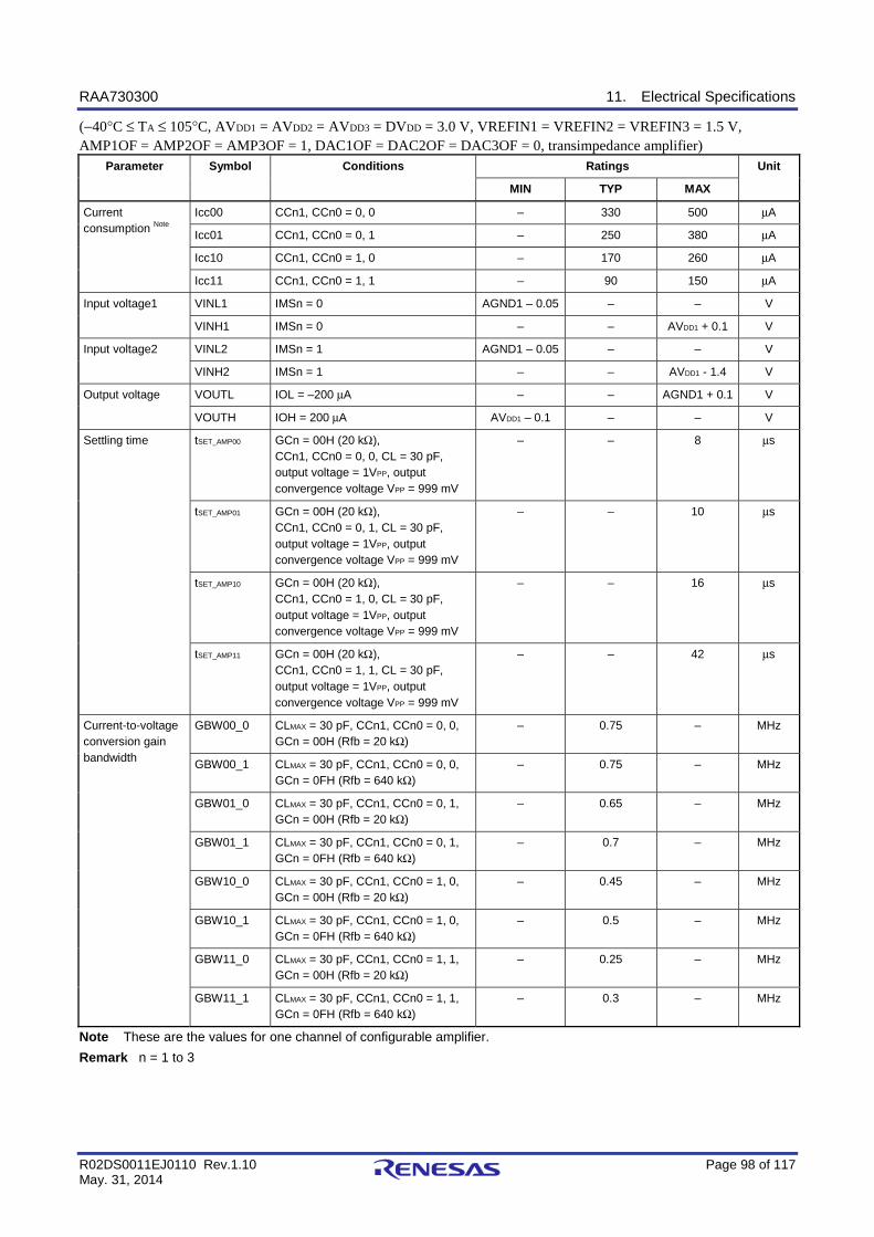
RAA730300 11. Electrical Specifications
R02DS0011EJ0110 Rev.1.10 Page 98 of 117 May. 31, 2014
(−40°C ≤ TA ≤ 105°C, AVDD1 = AVDD2 = AVDD3 = DVDD = 3.0 V, VREFIN1 = VREFIN2 = VREFIN3 = 1.5 V, AMP1OF = AMP2OF = AMP3OF = 1, DAC1OF = DAC2OF = DAC3OF = 0, transimpedance amplifier)
Parameter Symbol Conditions Ratings Unit
MIN TYP MAX
Current consumption Note
Icc00 CCn1, CCn0 = 0, 0 – 330 500 μA
Icc01 CCn1, CCn0 = 0, 1 – 250 380 μA
Icc10 CCn1, CCn0 = 1, 0 – 170 260 μA
Icc11 CCn1, CCn0 = 1, 1 – 90 150 μA
Input voltage1 VINL1 IMSn = 0 AGND1 – 0.05 – – V
VINH1 IMSn = 0 – – AVDD1 + 0.1 V
Input voltage2 VINL2 IMSn = 1 AGND1 – 0.05 – – V
VINH2 IMSn = 1 – – AVDD1 - 1.4 V
Output voltage VOUTL IOL = –200 μA – – AGND1 + 0.1 V
VOUTH IOH = 200 μA AVDD1 – 0.1 – – V
Settling time tSET_AMP00 GCn = 00H (20 kΩ), CCn1, CCn0 = 0, 0, CL = 30 pF, output voltage = 1VPP, output convergence voltage VPP = 999 mV
– – 8 μs
tSET_AMP01 GCn = 00H (20 kΩ), CCn1, CCn0 = 0, 1, CL = 30 pF, output voltage = 1VPP, output convergence voltage VPP = 999 mV
– – 10 μs
tSET_AMP10 GCn = 00H (20 kΩ), CCn1, CCn0 = 1, 0, CL = 30 pF, output voltage = 1VPP, output convergence voltage VPP = 999 mV
– – 16 μs
tSET_AMP11 GCn = 00H (20 kΩ), CCn1, CCn0 = 1, 1, CL = 30 pF, output voltage = 1VPP, output convergence voltage VPP = 999 mV
– – 42 μs
Current-to-voltage conversion gain bandwidth
GBW00_0 CLMAX = 30 pF, CCn1, CCn0 = 0, 0, GCn = 00H (Rfb = 20 kΩ)
– 0.75 – MHz
GBW00_1 CLMAX = 30 pF, CCn1, CCn0 = 0, 0, GCn = 0FH (Rfb = 640 kΩ)
– 0.75 – MHz
GBW01_0 CLMAX = 30 pF, CCn1, CCn0 = 0, 1, GCn = 00H (Rfb = 20 kΩ)
– 0.65 – MHz
GBW01_1 CLMAX = 30 pF, CCn1, CCn0 = 0, 1, GCn = 0FH (Rfb = 640 kΩ)
– 0.7 – MHz
GBW10_0 CLMAX = 30 pF, CCn1, CCn0 = 1, 0, GCn = 00H (Rfb = 20 kΩ)
– 0.45 – MHz
GBW10_1 CLMAX = 30 pF, CCn1, CCn0 = 1, 0, GCn = 0FH (Rfb = 640 kΩ)
– 0.5 – MHz
GBW11_0 CLMAX = 30 pF, CCn1, CCn0 = 1, 1, GCn = 00H (Rfb = 20 kΩ)
– 0.25 – MHz
GBW11_1 CLMAX = 30 pF, CCn1, CCn0 = 1, 1, GCn = 0FH (Rfb = 640 kΩ)
– 0.3 – MHz
Note These are the values for one channel of configurable amplifier. Remark n = 1 to 3
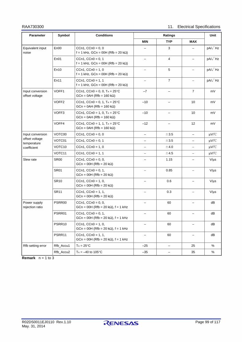
RAA730300 11. Electrical Specifications
R02DS0011EJ0110 Rev.1.10 Page 99 of 117 May. 31, 2014
Parameter Symbol Conditions Ratings Unit
MIN TYP MAX
Equivalent input noise
En00 CCn1, CCn0 = 0, 0 f = 1 kHz, GCn = 00H (Rfb = 20 kΩ)
– 3 – pA/√Hz
En01 CCn1, CCn0 = 0, 1 f = 1 kHz, GCn = 00H (Rfb = 20 kΩ)
– 4 – pA/√Hz
En10 CCn1, CCn0 = 1, 0 f = 1 kHz, GCn = 00H (Rfb = 20 kΩ)
– 5 – pA/√Hz
En11 CCn1, CCn0 = 1, 1 f = 1 kHz, GCn = 00H (Rfb = 20 kΩ)
– 7 – pA/√Hz
Input conversion offset voltage
VOFF1 CCn1, CCn0 = 0, 0, TA = 25°C GCn = 0AH (Rfb = 160 kΩ)
–7 – 7 mV
VOFF2 CCn1, CCn0 = 0, 1, TA = 25°C GCn = 0AH (Rfb = 160 kΩ)
–10 – 10 mV
VOFF3 CCn1, CCn0 = 1, 0, TA = 25°C GCn = 0AH (Rfb = 160 kΩ)
–10 – 10 mV
VOFF4 CCn1, CCn0 = 1, 1, TA = 25°C GCn = 0AH (Rfb = 160 kΩ)
–12 – 12 mV
Input conversion offset voltage temperature coefficient
VOTC00 CCn1, CCn0 = 0, 0 – ±3.5 – μV/℃
VOTC01 CCn1, CCn0 = 0, 1 – ±3.5 – μV/℃
VOTC10 CCn1, CCn0 = 1, 0 – ±4.0 – μV/℃
VOTC11 CCn1, CCn0 = 1, 1 – ±4.5 – μV/℃
Slew rate SR00 CCn1, CCn0 = 0, 0, GCn = 00H (Rfb = 20 kΩ)
– 1.15 – V/μs
SR01 CCn1, CCn0 = 0, 1, GCn = 00H (Rfb = 20 kΩ)
– 0.85 – V/μs
SR10 CCn1, CCn0 = 1, 0, GCn = 00H (Rfb = 20 kΩ)
– 0.6 – V/μs
SR11 CCn1, CCn0 = 1, 1, GCn = 00H (Rfb = 20 kΩ)
– 0.3 – V/μs
Power supply rejection ratio
PSRR00 CCn1, CCn0 = 0, 0, GCn = 00H (Rfb = 20 kΩ), f = 1 kHz
– 60 – dB
PSRR01 CCn1, CCn0 = 0, 1, GCn = 00H (Rfb = 20 kΩ), f = 1 kHz
– 60 – dB
PSRR10 CCn1, CCn0 = 1, 0, GCn = 00H (Rfb = 20 kΩ), f = 1 kHz
– 60 – dB
PSRR11 CCn1, CCn0 = 1, 1, GCn = 00H (Rfb = 20 kΩ), f = 1 kHz
– 60 – dB
Rfb setting error Rfb_Accu1 TA = 25°C –25 – 25 %
Rfb_Accu2 TA = –40 to 105°C –35 – 35 %
Remark n = 1 to 3

RAA730300 11. Electrical Specifications
R02DS0011EJ0110 Rev.1.10 Page 100 of 117 May. 31, 2014
(−40°C ≤ TA ≤ 105°C, AVDD1 = AVDD2 = AVDD3 = DVDD = 3.0 V, VREFIN1 = VREFIN2 = VREFIN3 = 1.5 V, AMP1OF = AMP2OF = AMP3OF = 1, DAC1OF = DAC2OF = DAC3OF = 0, GC1 = GC2 = 00H, instrumentation amplifier)
Parameter Symbol Conditions Ratings Unit
MIN TYP MAX
Current consumption
Icc00 AMP1OF = AMP2OF = AMP3OF = 1, CCn1, CCn0 = 0, 0
– 960 1400 μA
Icc01 AMP1OF = AMP2OF = AMP3OF = 1, CCn1, CCn0 = 0, 1
– 750 1100 μA
Icc10 AMP1OF = AMP2OF = AMP3OF = 1, CCn1, CCn0 = 1, 0
– 520 750 μA
Icc11 AMP1OF = AMP2OF = AMP3OF = 1, CCn1, CCn0 = 1, 1
– 310 450 μA
Input voltage 1 VINL1 IMSn = 0 AGND1 – 0.05 – – V
VINH1 IMSn = 0 – – AVDD1 + 0.1 V
Input voltage 2 VINL2 IMSn = 1 AGND1 – 0.05 – – V
VINH2 IMSn = 1 – – AVDD1 – 1.4 V
Output voltage VOUTL IOL = –200 μA – – AGND1 + 0.05 V
VOUTH IOH = 200 μA AVDD1 – 0.05 – – V
Settling time tSET_AMP00 GCn = 00H (15.5 dB), CCn1, CCn0 = 0, 0, CL = 30 pF, output voltage = 1VPP, output convergence voltage VPP = 999 mV
– – 9 μs
tSET_AMP01 GCn = 00H (15.5 dB), CCn1, CCn0 = 0, 1, CL = 30 pF, output voltage = 1VPP, output convergence voltage VPP = 999 mV
– – 12 μs
tSET_AMP10 GCn = 00H (15.5 dB), CCn1, CCn0 = 1, 0, CL = 30 pF, output voltage = 1VPP, output convergence voltage VPP = 999 mV
– – 20 μs
tSET_AMP11 GCn = 00H (15.5 dB), CCn1, CCn0 = 1, 1, CL = 30 pF, output voltage = 1VPP, output convergence voltage VPP = 999 mV
– – 56 μs
Gain bandwidth GBW00 CLMAX = 30 pF, CCn1, CCn0 = 0, 0 GC3 = 09H (33.5 dB)
– 1.0 – MHz
GBW01 CLMAX = 30 pF, CCn1, CCn0 = 0, 1
GC3 = 09H (33.5 dB)
– 0.9 – MHz
GBW10 CLMAX = 30 pF, CCn1, CCn0 = 1, 0
GC3 = 09H (33.5 dB)
– 0.65 – MHz
GBW11 CLMAX = 30 pF, CCn1, CCn0 = 1, 1
GC3 = 09H (33.5 dB)
– 0.35 – MHz
Equivalent input noise
En00 CCn1, CCn0 = 0, 0
GC3 = 09H (33.5 dB), f = 1 kHz
– 95 – nV/√ Hz
En01 CCn1, CCn0 = 0, 1
GC3 = 09H (33.5 dB), f = 1 kHz
– 110 – nV/√ Hz
En10 CCn1, CCn0 = 1, 0
GC3 = 09H (33.5 dB), f = 1 kHz
– 135 – nV/√ Hz
En11 CCn1, CCn0 = 1, 1
GC3 = 09H (33.5 dB), f = 1 kHz
– 200 – nV/√ Hz
Remark n = 1 to 3
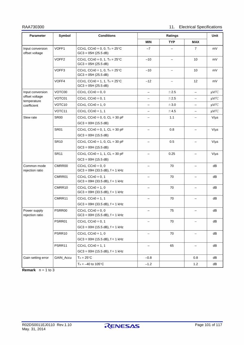
RAA730300 11. Electrical Specifications
R02DS0011EJ0110 Rev.1.10 Page 101 of 117 May. 31, 2014
Parameter Symbol Conditions Ratings Unit
MIN TYP MAX
Input conversion offset voltage
VOFF1 CCn1, CCn0 = 0, 0, TA = 25°C GC3 = 05H (25.5 dB)
–7 – 7 mV
VOFF2 CCn1, CCn0 = 0, 1, TA = 25°C GC3 = 05H (25.5 dB)
–10 – 10 mV
VOFF3 CCn1, CCn0 = 1, 0, TA = 25°C GC3 = 05H (25.5 dB)
–10 – 10 mV
VOFF4 CCn1, CCn0 = 1, 1, TA = 25°C GC3 = 05H (25.5 dB)
–12 – 12 mV
Input conversion offset voltage temperature coefficient
VOTC00 CCn1, CCn0 = 0, 0 – ±2.5 – μV/℃
VOTC01 CCn1, CCn0 = 0, 1 – ±2.5 – μV/℃
VOTC10 CCn1, CCn0 = 1, 0 – ±3.0 – μV/℃
VOTC11 CCn1, CCn0 = 1, 1 – ±4.5 – μV/℃
Slew rate SR00 CCn1, CCn0 = 0, 0, CL = 30 pF
GC3 = 00H (15.5 dB)
– 1.1 – V/μs
SR01 CCn1, CCn0 = 0, 1, CL = 30 pF
GC3 = 00H (15.5 dB)
– 0.8 – V/μs
SR10 CCn1, CCn0 = 1, 0, CL = 30 pF
GC3 = 00H (15.5 dB)
– 0.5 – V/μs
SR11 CCn1, CCn0 = 1, 1, CL = 30 pF
GC3 = 00H (15.5 dB)
– 0.25 – V/μs
Common mode rejection ratio
CMRR00 CCn1, CCn0 = 0, 0 GC3 = 09H (33.5 dB), f = 1 kHz
– 70 – dB
CMRR01 CCn1, CCn0 = 0, 1 GC3 = 09H (33.5 dB), f = 1 kHz
– 70 – dB
CMRR10 CCn1, CCn0 = 1, 0 GC3 = 09H (33.5 dB), f = 1 kHz
– 70 – dB
CMRR11 CCn1, CCn0 = 1, 1
GC3 = 09H (33.5 dB), f = 1 kHz
– 70 – dB
Power supply rejection ratio
PSRR00 CCn1, CCn0 = 0, 0 GC3 = 00H (15.5 dB), f = 1 kHz
– 75 – dB
PSRR01 CCn1, CCn0 = 0, 1
GC3 = 00H (15.5 dB), f = 1 kHz
– 70 – dB
PSRR10 CCn1, CCn0 = 1, 0
GC3 = 00H (15.5 dB), f = 1 kHz
– 70 – dB
PSRR11 CCn1, CCn0 = 1, 1
GC3 = 00H (15.5 dB), f = 1 kHz
– 65 – dB
Gain setting error GAIN_Accu TA = 25°C –0.8 0.8 dB
TA = –40 to 105°C –1.2 1.2 dB
Remark n = 1 to 3
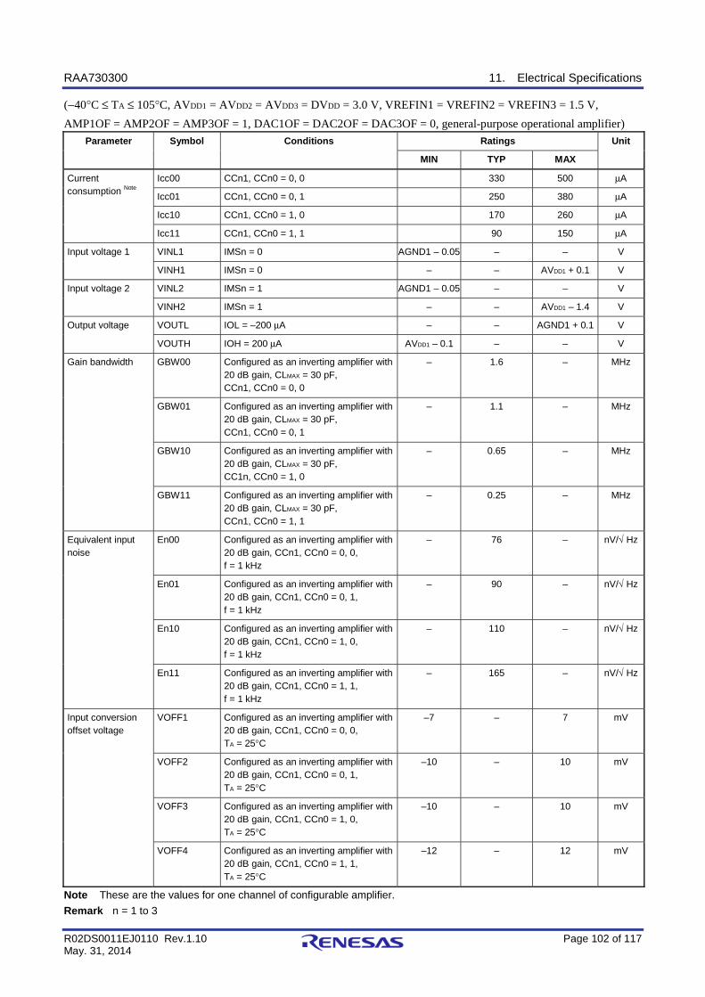
RAA730300 11. Electrical Specifications
R02DS0011EJ0110 Rev.1.10 Page 102 of 117 May. 31, 2014
(−40°C ≤ TA ≤ 105°C, AVDD1 = AVDD2 = AVDD3 = DVDD = 3.0 V, VREFIN1 = VREFIN2 = VREFIN3 = 1.5 V,
AMP1OF = AMP2OF = AMP3OF = 1, DAC1OF = DAC2OF = DAC3OF = 0, general-purpose operational amplifier)
Parameter Symbol Conditions Ratings Unit
MIN TYP MAX
Current consumption Note
Icc00 CCn1, CCn0 = 0, 0 330 500 μA
Icc01 CCn1, CCn0 = 0, 1 250 380 μA
Icc10 CCn1, CCn0 = 1, 0 170 260 μA
Icc11 CCn1, CCn0 = 1, 1 90 150 μA
Input voltage 1 VINL1 IMSn = 0 AGND1 – 0.05 – – V
VINH1 IMSn = 0 – – AVDD1 + 0.1 V
Input voltage 2 VINL2 IMSn = 1 AGND1 – 0.05 – – V
VINH2 IMSn = 1 – – AVDD1 – 1.4 V
Output voltage VOUTL IOL = –200 μA – – AGND1 + 0.1 V
VOUTH IOH = 200 μA AVDD1 – 0.1 – – V
Gain bandwidth GBW00 Configured as an inverting amplifier with 20 dB gain, CLMAX = 30 pF, CCn1, CCn0 = 0, 0
– 1.6 – MHz
GBW01 Configured as an inverting amplifier with 20 dB gain, CLMAX = 30 pF, CCn1, CCn0 = 0, 1
– 1.1 – MHz
GBW10 Configured as an inverting amplifier with 20 dB gain, CLMAX = 30 pF, CC1n, CCn0 = 1, 0
– 0.65 – MHz
GBW11 Configured as an inverting amplifier with 20 dB gain, CLMAX = 30 pF, CCn1, CCn0 = 1, 1
– 0.25 – MHz
Equivalent input noise
En00 Configured as an inverting amplifier with 20 dB gain, CCn1, CCn0 = 0, 0, f = 1 kHz
– 76 – nV/√ Hz
En01 Configured as an inverting amplifier with 20 dB gain, CCn1, CCn0 = 0, 1, f = 1 kHz
– 90 – nV/√ Hz
En10 Configured as an inverting amplifier with 20 dB gain, CCn1, CCn0 = 1, 0, f = 1 kHz
– 110 – nV/√ Hz
En11 Configured as an inverting amplifier with 20 dB gain, CCn1, CCn0 = 1, 1, f = 1 kHz
– 165 – nV/√ Hz
Input conversion offset voltage
VOFF1 Configured as an inverting amplifier with 20 dB gain, CCn1, CCn0 = 0, 0, TA = 25°C
–7 – 7 mV
VOFF2 Configured as an inverting amplifier with 20 dB gain, CCn1, CCn0 = 0, 1, TA = 25°C
–10 – 10 mV
VOFF3 Configured as an inverting amplifier with 20 dB gain, CCn1, CCn0 = 1, 0, TA = 25°C
–10 – 10 mV
VOFF4 Configured as an inverting amplifier with 20 dB gain, CCn1, CCn0 = 1, 1, TA = 25°C
–12 – 12 mV
Note These are the values for one channel of configurable amplifier. Remark n = 1 to 3
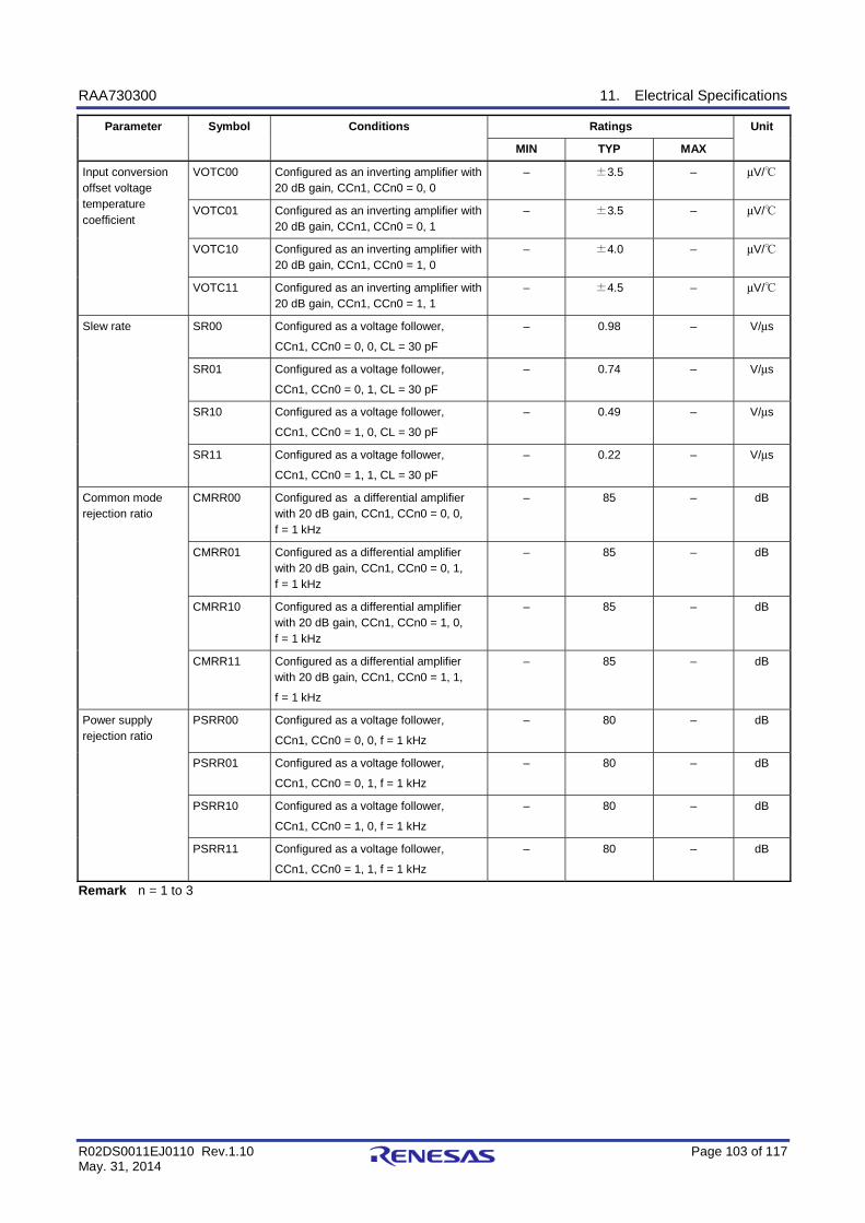
RAA730300 11. Electrical Specifications
R02DS0011EJ0110 Rev.1.10 Page 103 of 117 May. 31, 2014
Parameter Symbol Conditions Ratings Unit
MIN TYP MAX
Input conversion offset voltage temperature coefficient
VOTC00 Configured as an inverting amplifier with 20 dB gain, CCn1, CCn0 = 0, 0
– ±3.5 – μV/℃
VOTC01 Configured as an inverting amplifier with 20 dB gain, CCn1, CCn0 = 0, 1
– ±3.5 – μV/℃
VOTC10 Configured as an inverting amplifier with 20 dB gain, CCn1, CCn0 = 1, 0
– ±4.0 – μV/℃
VOTC11 Configured as an inverting amplifier with 20 dB gain, CCn1, CCn0 = 1, 1
– ±4.5 – μV/℃
Slew rate SR00 Configured as a voltage follower,
CCn1, CCn0 = 0, 0, CL = 30 pF
– 0.98 – V/μs
SR01 Configured as a voltage follower,
CCn1, CCn0 = 0, 1, CL = 30 pF
– 0.74 – V/μs
SR10 Configured as a voltage follower,
CCn1, CCn0 = 1, 0, CL = 30 pF
– 0.49 – V/μs
SR11 Configured as a voltage follower,
CCn1, CCn0 = 1, 1, CL = 30 pF
– 0.22 – V/μs
Common mode rejection ratio
CMRR00 Configured as a differential amplifier with 20 dB gain, CCn1, CCn0 = 0, 0, f = 1 kHz
– 85 – dB
CMRR01 Configured as a differential amplifier with 20 dB gain, CCn1, CCn0 = 0, 1, f = 1 kHz
– 85 – dB
CMRR10 Configured as a differential amplifier with 20 dB gain, CCn1, CCn0 = 1, 0, f = 1 kHz
– 85 – dB
CMRR11 Configured as a differential amplifier with 20 dB gain, CCn1, CCn0 = 1, 1,
f = 1 kHz
– 85 – dB
Power supply rejection ratio
PSRR00 Configured as a voltage follower,
CCn1, CCn0 = 0, 0, f = 1 kHz
– 80 – dB
PSRR01 Configured as a voltage follower,
CCn1, CCn0 = 0, 1, f = 1 kHz
– 80 – dB
PSRR10 Configured as a voltage follower,
CCn1, CCn0 = 1, 0, f = 1 kHz
– 80 – dB
PSRR11 Configured as a voltage follower,
CCn1, CCn0 = 1, 1, f = 1 kHz
– 80 – dB
Remark n = 1 to 3

RAA730300 11. Electrical Specifications
R02DS0011EJ0110 Rev.1.10 Page 104 of 117 May. 31, 2014
(2) General-purpose operational amplifier
(−40°C ≤ TA ≤ 105°C, AVDD1 = AVDD2 = AVDD3 = DVDD = 3.0 V, AMP4OF = AMP5OF = 1) Parameter Symbol Conditions Ratings Unit
MIN TYP MAX
Current consumption
IccA 320 450 μA
Input voltage 1 VINL1 IMSn = 0 AGND1 – 0.05 – – V
VINH1 IMSn = 0 – – AVDD1 + 0.1 V
Input voltage 2 VINL2 IMSn = 1 AGND1 – 0.05 – – V
VINH2 IMSn = 1 – – AVDD1 – 1.4 V
Output voltage VOUTL IOL = –200 μA – – AGND1 + 0.05 V
VOUTH IOH = 200 μA AVDD1 – 0.05 – – V
Gain bandwidth GBW Configured as an inverting amplifier with 20 dB gain, CLMAX = 30 pF
– 2.0 – MHz
Input conversion offset voltage
VOFF Configured as an inverting amplifier with 20 dB gain, TA = 25°C, AMP4_INP = AMP5_INP = 1.5 V
–7 – 7 mV
Input conversion offset voltage temperature coefficient
VOTC Configured as an inverting amplifier with 20 dB gain
– ±2.0 – μV/°C
Slew rate SR Configured as a voltage follower,
CL = 30 pF
– 0.9 – V/μs
Equivalent input noise
En_Gain Configured as an inverting amplifier with 20 dB gain, f = 1 kHz
– 77 – nV/√ Hz
Common mode rejection ratio
CMRR Configured as a differential amplifier with 20 dB gain, f = 1 kHz
– 75 – dB
Power supply rejection ratio
PSRR Configured as an inverting amplifier with 20 dB gain, f = 1 kHz
– 55 – dB
Remark n = 4, 5
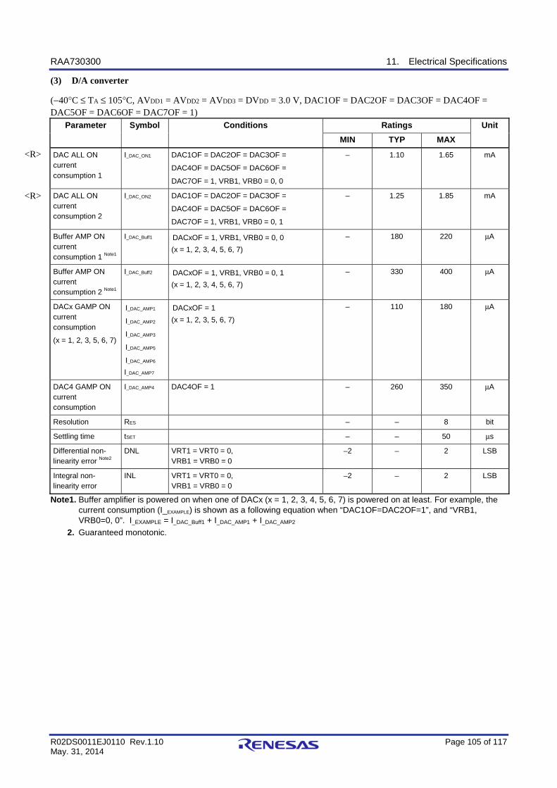
RAA730300 11. Electrical Specifications
R02DS0011EJ0110 Rev.1.10 Page 105 of 117 May. 31, 2014
(3) D/A converter
(−40°C ≤ TA ≤ 105°C, AVDD1 = AVDD2 = AVDD3 = DVDD = 3.0 V, DAC1OF = DAC2OF = DAC3OF = DAC4OF = DAC5OF = DAC6OF = DAC7OF = 1)
Parameter Symbol Conditions Ratings Unit
MIN TYP MAX
DAC ALL ON current consumption 1
I_DAC_ON1 DAC1OF = DAC2OF = DAC3OF =
DAC4OF = DAC5OF = DAC6OF =
DAC7OF = 1, VRB1, VRB0 = 0, 0
– 1.10 1.65 mA
DAC ALL ON current consumption 2
I_DAC_ON2 DAC1OF = DAC2OF = DAC3OF =
DAC4OF = DAC5OF = DAC6OF =
DAC7OF = 1, VRB1, VRB0 = 0, 1
– 1.25 1.85 mA
Buffer AMP ON current consumption 1 Note1
I_DAC_Buff1 DACxOF = 1, VRB1, VRB0 = 0, 0 (x = 1, 2, 3, 4, 5, 6, 7)
– 180 220 μA
Buffer AMP ON current consumption 2 Note1
I_DAC_Buff2 DACxOF = 1, VRB1, VRB0 = 0, 1 (x = 1, 2, 3, 4, 5, 6, 7)
– 330 400 μA
DACx GAMP ON current consumption
(x = 1, 2, 3, 5, 6, 7)
I_DAC_AMP1
I_DAC_AMP2
I_DAC_AMP3
I_DAC_AMP5
I_DAC_AMP6 I_DAC_AMP7
DACxOF = 1 (x = 1, 2, 3, 5, 6, 7)
– 110 180 μA
DAC4 GAMP ON current consumption
I_DAC_AMP4 DAC4OF = 1 – 260 350 μA
Resolution RES – – 8 bit
Settling time tSET – – 50 μs
Differential non-linearity error Note2
DNL VRT1 = VRT0 = 0, VRB1 = VRB0 = 0
–2 – 2 LSB
Integral non-linearity error
INL VRT1 = VRT0 = 0, VRB1 = VRB0 = 0
–2 – 2 LSB
Note1. Buffer amplifier is powered on when one of DACx (x = 1, 2, 3, 4, 5, 6, 7) is powered on at least. For example, the current consumption (I_EXAMPLE) is shown as a following equation when “DAC1OF=DAC2OF=1”, and “VRB1, VRB0=0, 0”. I_EXAMPLE = I_DAC_Buff1 + I_DAC_AMP1 + I_DAC_AMP2
2. Guaranteed monotonic.
<R>
<R>

RAA730300 11. Electrical Specifications
R02DS0011EJ0110 Rev.1.10 Page 106 of 117 May. 31, 2014
(4) Low-pass filter
(−40°C ≤ TA ≤ 105°C, AVDD1 = AVDD2 = AVDD3 = DVDD = 3.0 V, LPFOF = 1) Parameter Symbol Conditions Ratings Unit
MIN TYP MAX
Current consumption IccA – 800 1200 μA
Input voltage 1 VILLPF1 IMSn = 0 AGND4 + 0.2 – – V
VIHLPF1 IMSn = 0 – – AVDD3 – 0.2 V
Input voltage 2 VILLPF2 IMSn = 1 AGND4 + 0.2 – – V
VIHLPF2 IMSn = 1 – – AVDD3 – 1.4 V
Output voltage VOLLPF IOL = –200 μA – – AGND4 – 0.2 V
VOHLPF IOH = 200 μA AVDD3 – 0.2 – – V
Input conversion offset voltage
VOFF DAC4OF = 1, DAC4C = 80H -100 – 100 mV
Cutoff frequency fc1 fCLK_LPF = 2 kHz – 8.7 – Hz
fc2 fCLK_LPF = 200 kHz – 870 – Hz
CLK_LPF
low-level
input voltage
VILCLK_LPF 0.3 × AVDD3 V
CLK_LPF
high-level
input voltage
VIHCLK_LPF 0.7 × AVDD3 V
CLK_LPF
Input frequency
fCLK_LPF 2 – 200 kHz
CLK_LPF
Input low-level-width Input high-level-width
tILW_LPF
tIHW_LPF
200 – – ns
Remark n = 6
Clock Timing
CLK_LPF
0.3VDD
0.7VDD
tILW_LPF tIHW_LPF
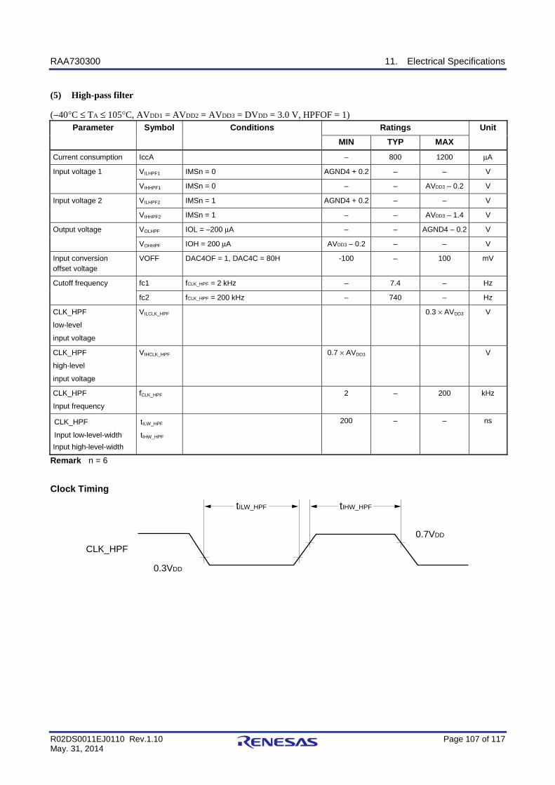
RAA730300 11. Electrical Specifications
R02DS0011EJ0110 Rev.1.10 Page 107 of 117 May. 31, 2014
(5) High-pass filter
(−40°C ≤ TA ≤ 105°C, AVDD1 = AVDD2 = AVDD3 = DVDD = 3.0 V, HPFOF = 1) Parameter Symbol Conditions Ratings Unit
MIN TYP MAX
Current consumption IccA – 800 1200 μA
Input voltage 1 VILHPF1 IMSn = 0 AGND4 + 0.2 – – V
VIHHPF1 IMSn = 0 – – AVDD3 – 0.2 V
Input voltage 2 VILHPF2 IMSn = 1 AGND4 + 0.2 – – V
VIHHPF2 IMSn = 1 – – AVDD3 – 1.4 V
Output voltage VOLHPF IOL = –200 μA – – AGND4 – 0.2 V
VOHHPF IOH = 200 μA AVDD3 – 0.2 – – V
Input conversion offset voltage
VOFF DAC4OF = 1, DAC4C = 80H -100 – 100 mV
Cutoff frequency fc1 fCLK_HPF = 2 kHz – 7.4 – Hz
fc2 fCLK_HPF = 200 kHz – 740 – Hz
CLK_HPF
low-level
input voltage
VILCLK_HPF 0.3 × AVDD3 V
CLK_HPF
high-level
input voltage
VIHCLK_HPF 0.7 × AVDD3 V
CLK_HPF
Input frequency
fCLK_HPF 2 – 200 kHz
CLK_HPF
Input low-level-width Input high-level-width
tILW_HPF
tIHW_HPF
200 – – ns
Remark n = 6
Clock Timing
CLK_HPF
0.3VDD
0.7VDD
tILW_HPF tIHW_HPF
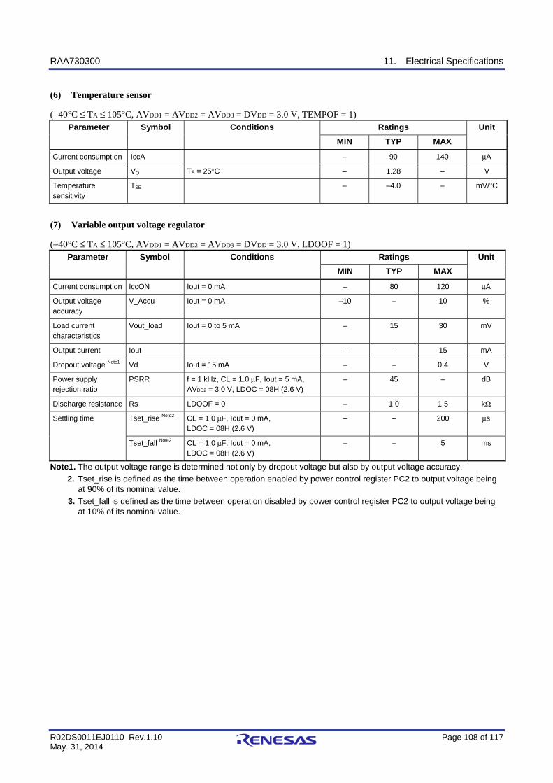
RAA730300 11. Electrical Specifications
R02DS0011EJ0110 Rev.1.10 Page 108 of 117 May. 31, 2014
(6) Temperature sensor
(−40°C ≤ TA ≤ 105°C, AVDD1 = AVDD2 = AVDD3 = DVDD = 3.0 V, TEMPOF = 1) Parameter Symbol Conditions Ratings Unit
MIN TYP MAX
Current consumption IccA – 90 140 μA
Output voltage VO TA = 25°C – 1.28 – V
Temperature sensitivity
TSE – –4.0 – mV/°C
(7) Variable output voltage regulator
(−40°C ≤ TA ≤ 105°C, AVDD1 = AVDD2 = AVDD3 = DVDD = 3.0 V, LDOOF = 1) Parameter Symbol Conditions Ratings Unit
MIN TYP MAX
Current consumption IccON Iout = 0 mA – 80 120 μA
Output voltage accuracy
V_Accu Iout = 0 mA –10 – 10 %
Load current characteristics
Vout_load Iout = 0 to 5 mA – 15 30 mV
Output current Iout – – 15 mA
Dropout voltage Note1 Vd Iout = 15 mA – – 0.4 V
Power supply rejection ratio
PSRR f = 1 kHz, CL = 1.0 μF, Iout = 5 mA, AVDD2 = 3.0 V, LDOC = 08H (2.6 V)
– 45 – dB
Discharge resistance Rs LDOOF = 0 – 1.0 1.5 kΩ
Settling time Tset_rise Note2 CL = 1.0 μF, Iout = 0 mA, LDOC = 08H (2.6 V)
– – 200 μs
Tset_fall Note2 CL = 1.0 μF, Iout = 0 mA, LDOC = 08H (2.6 V)
– – 5 ms
Note1. The output voltage range is determined not only by dropout voltage but also by output voltage accuracy. 2. Tset_rise is defined as the time between operation enabled by power control register PC2 to output voltage being
at 90% of its nominal value. 3. Tset_fall is defined as the time between operation disabled by power control register PC2 to output voltage being
at 10% of its nominal value.
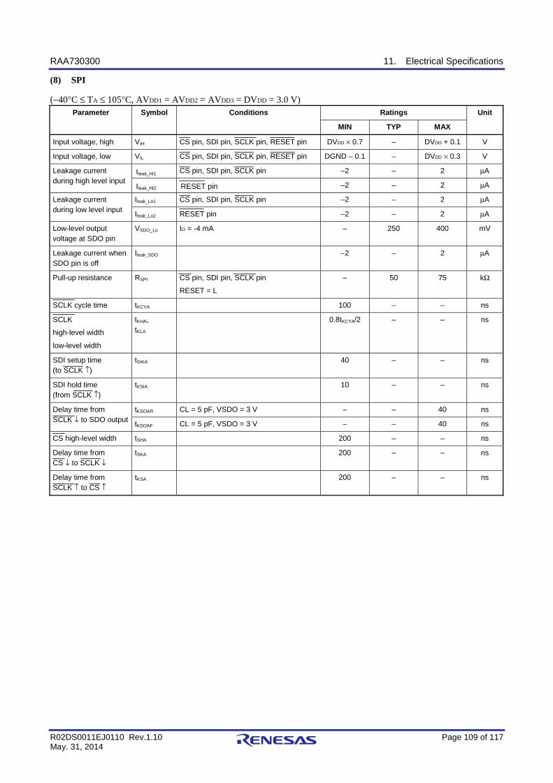
RAA730300 11. Electrical Specifications
R02DS0011EJ0110 Rev.1.10 Page 109 of 117 May. 31, 2014
(8) SPI
(−40°C ≤ TA ≤ 105°C, AVDD1 = AVDD2 = AVDD3 = DVDD = 3.0 V) Parameter Symbol Conditions Ratings Unit
MIN TYP MAX
Input voltage, high VIH CS pin, SDI pin, SCLK pin, RESET pin DVDD × 0.7 – DVDD + 0.1 V
Input voltage, low VIL CS pin, SDI pin, SCLK pin, RESET pin DGND – 0.1 – DVDD × 0.3 V
Leakage current during high level input
Ileak_Hi1 CS pin, SDI pin, SCLK pin –2 – 2 μA
Ileak_Hi2 RESET pin –2 – 2 μA
Leakage current during low level input
Ileak_Lo1 CS pin, SDI pin, SCLK pin –2 – 2 μA
Ileak_Lo2 RESET pin –2 – 2 μA
Low-level output voltage at SDO pin
VSDO_Lo IO = -4 mA – 250 400 mV
Leakage current when SDO pin is off
Ileak_SDO –2 – 2 μA
Pull-up resistance RSPI CS pin, SDI pin, SCLK pin
RESET = L
– 50 75 kΩ
SCLK cycle time tKCYA 100 – – ns
SCLK
high-level width
low-level width
tKHA, tKLA
0.8tKCYA/2 – – ns
SDI setup time (to SCLK ↑)
tSIKA 40 – – ns
SDI hold time (from SCLK ↑)
tKSIA 10 – – ns
Delay time from SCLK ↓ to SDO output
tKSOAR CL = 5 pF, VSDO = 3 V – – 40 ns
tKSOAF CL = 5 pF, VSDO = 3 V – – 40 ns
CS high-level width tSHA 200 – – ns
Delay time from CS ↓ to SCLK ↓
tSKA 200 – – ns
Delay time from SCLK ↑ to CS ↑
tKSA 200 – – ns
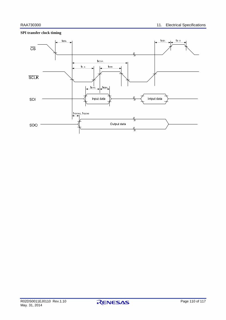
RAA730300 11. Electrical Specifications
R02DS0011EJ0110 Rev.1.10 Page 110 of 117 May. 31, 2014
SPI transfer clock timing
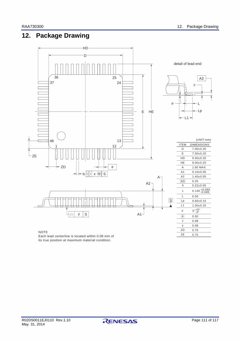
RAA730300 12. Package Drawing
R02DS0011EJ0110 Rev.1.10 Page 111 of 117 May. 31, 2014
12. Package Drawing
Sy
e
Sxb M
θ L
c
Lp
HD
HE
ZD
ZE
L1
A1
A2
A
D
E
A3
S
0.145 +0.055-0.045
(UNIT:mm)
ITEM DIMENSIONSDE
HDHEA
A1A2A3
7.00±0.207.00±0.209.00±0.209.00±0.201.60 MAX.0.10±0.051.40±0.050.25
c
θ
exy
ZDZE
0.500.080.080.750.75
LLpL1
0.500.60±0.151.00±0.20
3°+5°-3°
NOTEEach lead centerline is located within 0.08 mm ofits true position at maximum material condition.
detail of lead end
0.22±0.05b
12
24
148 13
2537
36
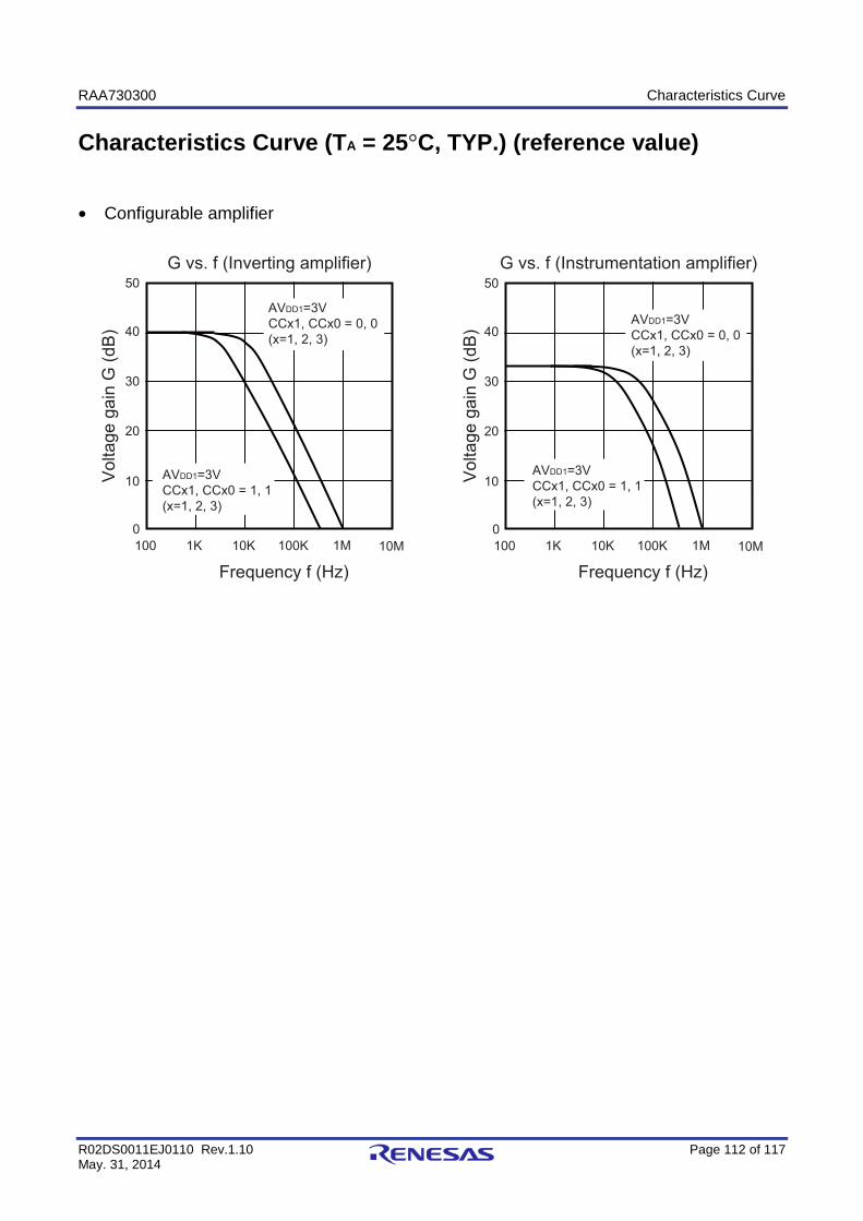
RAA730300 Characteristics Curve
R02DS0011EJ0110 Rev.1.10 Page 112 of 117 May. 31, 2014
Characteristics Curve (TA = 25°C, TYP.) (reference value)
• Configurable amplifier
100 1K 10K 100K 1M 10M
10
20
30
40
50
010M
50
100K 1M
30
40
100 1K 10K
10
20
0
Vol
tage
gai
n G
(dB
)
Vol
tage
gai
n G
(dB
)
G vs. f (Inverting amplifier) G vs. f (Instrumentation amplifier)
AVDD1=3VCCx1, CCx0 = 0, 0(x=1, 2, 3)
AVDD1=3VCCx1, CCx0 = 0, 0(x=1, 2, 3)
AVDD1=3VCCx1, CCx0 = 1, 1(x=1, 2, 3)
AVDD1=3VCCx1, CCx0 = 1, 1(x=1, 2, 3)
Frequency f (Hz) Frequency f (Hz)
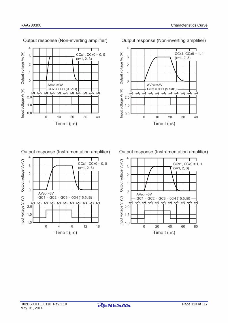
RAA730300 Characteristics Curve
R02DS0011EJ0110 Rev.1.10 Page 113 of 117 May. 31, 2014
1.0
2.0
0
1
2
3
Output response (Non-inverting amplifier)
Output response (Instrumentation amplifier)Output response (Instrumentation amplifier)
Output response (Non-inverting amplifier)
0 10 3020 40
4
0.00 10 20 30 40
1.0
2.0
0
1
2
3
4
0.0
1.5
2.0
0
1
2
3
4
0 4 128 161.0
0 20 40 60 80
1.5
2.0
0
1
2
3
4
1.0
Out
put v
olta
ge V
O (V
)In
put v
olta
ge V
I (V
)
Out
put v
olta
ge V
O (V
)In
put v
olta
ge V
I (V
)
Out
put v
olta
ge V
O (V
)In
put v
olta
ge V
I (V
)
Out
put v
olta
ge V
O (V
)In
put v
olta
ge V
I (V
)
AVDD1=3VGCx = 00H (9.5dB)
Time t (µs) Time t (µs)
Time t (µs) Time t (µs)
CCx1, CCx0 = 0, 0(x=1, 2, 3)
CCx1, CCx0 = 1, 1(x=1, 2, 3)
CCx1, CCx0 = 1, 1(x=1, 2, 3)
AVDD1=3VGCx = 00H (9.5dB)
CCx1, CCx0 = 0, 0(x=1, 2, 3)
AVDD1=3VGC1 = GC2 = GC3 = 00H (15.5dB)
AVDD1=3VGC1 = GC2 = GC3 = 00H (15.5dB)
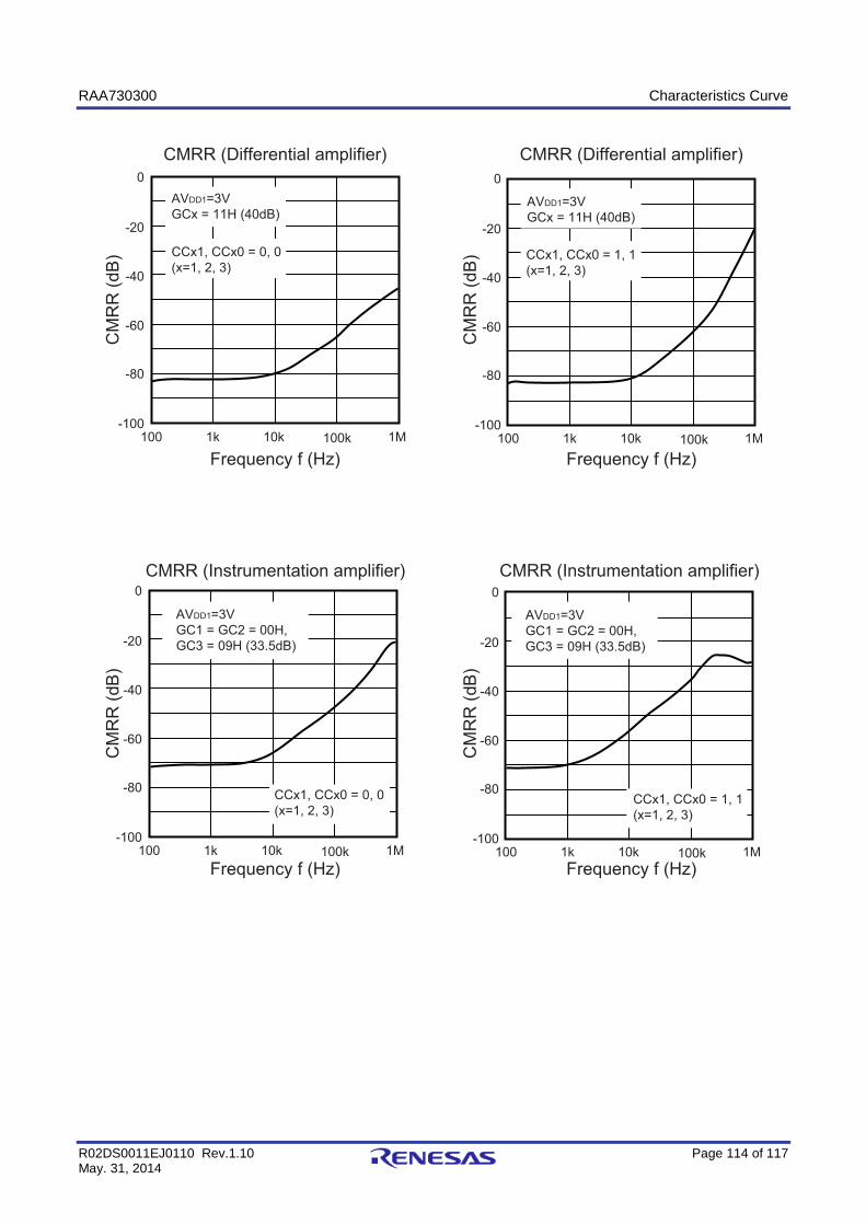
RAA730300 Characteristics Curve
R02DS0011EJ0110 Rev.1.10 Page 114 of 117 May. 31, 2014
100 1k 10k 100k 1M
0
-20
-40
-60
-80
-100100 1k 10k 100k 1M
0
-20
-40
-60
-80
-100
100 1k 10k 100k 1M
0
-20
-40
-60
-80
-100100 1k 10k 100k 1M
0
-20
-40
-60
-80
-100
CM
RR
(dB
)
CM
RR
(dB
)
CM
RR
(dB
)
CM
RR
(dB
)
AVDD1=3VGCx = 11H (40dB)
CCx1, CCx0 = 0, 0(x=1, 2, 3)
Frequency f (Hz) Frequency f (Hz)
Frequency f (Hz) Frequency f (Hz)
CMRR (Differential amplifier) CMRR (Differential amplifier)
CMRR (Instrumentation amplifier) CMRR (Instrumentation amplifier)
AVDD1=3VGCx = 11H (40dB)
CCx1, CCx0 = 1, 1(x=1, 2, 3)
AVDD1=3VGC1 = GC2 = 00H, GC3 = 09H (33.5dB)
CCx1, CCx0 = 0, 0(x=1, 2, 3)
AVDD1=3VGC1 = GC2 = 00H, GC3 = 09H (33.5dB)
CCx1, CCx0 = 1, 1(x=1, 2, 3)
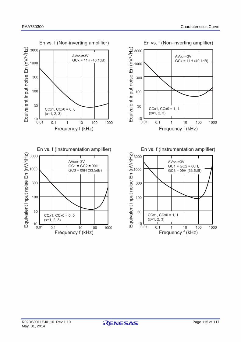
RAA730300 Characteristics Curve
R02DS0011EJ0110 Rev.1.10 Page 115 of 117 May. 31, 2014
0.01 0.1 1 10 100 1000 10
1000
100
300
30
3000
0.01 0.1 1 10 100 1000 10
1000
100
300
30
3000
1000
0.01 0.1 1 10 100 1000
100
10
300
30
3000
0.01 0.1 1 10 100 1000 10
1000
100
300
30
3000
En vs. f (Non-inverting amplifier) En vs. f (Non-inverting amplifier)
En vs. f (Instrumentation amplifier) En vs. f (Instrumentation amplifier)
Equ
ival
ent i
nput
noi
se E
n (n
V/√
Hz)
Equ
ival
ent i
nput
noi
se E
n (n
V/√
Hz)
Equ
ival
ent i
nput
noi
se E
n (n
V/√
Hz)
Equ
ival
ent i
nput
noi
se E
n (n
V/√
Hz)
Frequency f (kHz) Frequency f (kHz)
Frequency f (kHz) Frequency f (kHz)
AVDD1=3VGC1 = GC2 = 00H, GC3 = 09H (33.5dB)
AVDD1=3VGC1 = GC2 = 00H, GC3 = 09H (33.5dB)
CCx1, CCx0 = 1, 1(x=1, 2, 3)
CCx1, CCx0 = 0, 0(x=1, 2, 3)
CCx1, CCx0 = 1, 1(x=1, 2, 3)
CCx1, CCx0 = 0, 0(x=1, 2, 3)
AVDD1=3VGCx = 11H (40.1dB)
AVDD1=3VGCx = 11H (40.1dB)
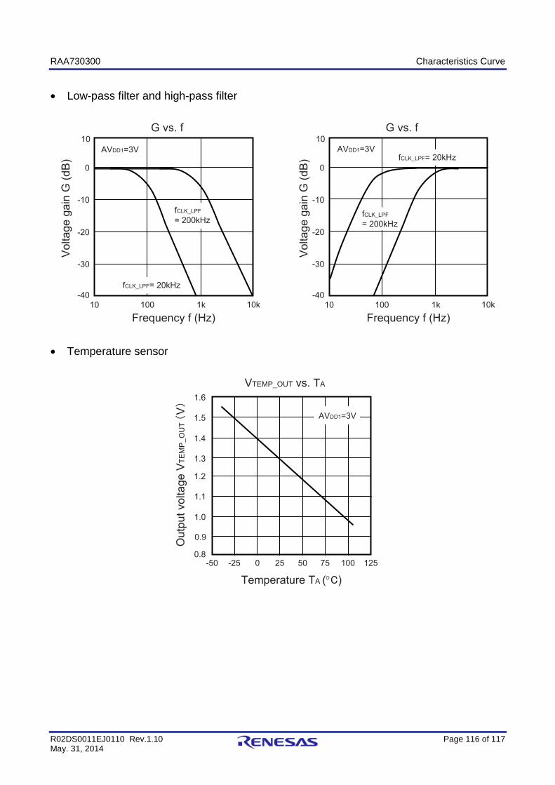
RAA730300 Characteristics Curve
R02DS0011EJ0110 Rev.1.10 Page 116 of 117 May. 31, 2014
• Low-pass filter and high-pass filter
10k10 100 1k
0
10
-10
-20
-30
-4010 100 1k 10k
0
10
-10
-20
-30
-40
G vs. f G vs. f
AVDD1=3V AVDD1=3VfCLK_LPF= 20kHz
fCLK_LPF
= 200kHz
Vol
tage
gai
n G
(dB
)
Vol
tage
gai
n G
(dB
)
fCLK_LPF
= 200kHz
fCLK_LPF= 20kHz
Frequency f (Hz) Frequency f (Hz)
• Temperature sensor
-50 -25 25 0 50 75 100 125
1.6
1.4
1.0
1.2
0.8
1.5
1.1
1.3
0.9
VTEMP_OUT vs. TA
Out
put v
olta
ge V
TEM
P_O
UT
V
Temperature TA (° )
AVDD1=3V
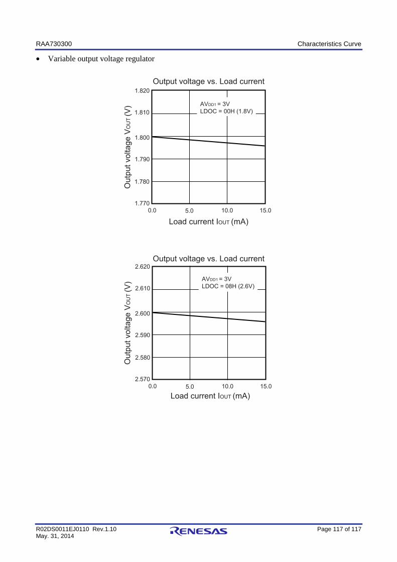
RAA730300 Characteristics Curve
R02DS0011EJ0110 Rev.1.10 Page 117 of 117 May. 31, 2014
• Variable output voltage regulator
5.0 10.0 15.0 1.770
0.0
1.780
1.790
1.800
1.810
1.820
5.0 10.0 15.0 2.570
0.0
2.580
2.590
2.600
2.610
2.620
Output voltage vs. Load current
Output voltage vs. Load current
AVDD1 = 3VLDOC = 00H (1.8V)
Load current IOUT (mA)
Load current IOUT (mA)
AVDD1 = 3VLDOC = 08H (2.6V)
Out
put v
olta
ge V
OU
T (V
)O
utpu
t vol
tage
VO
UT
(V)
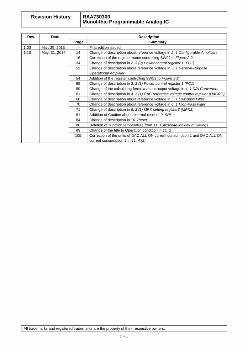
C - 1
Revision History RAA730300 Monolithic Programmable Analog IC
Rev. Date Description Page Summary
1.00 Mar. 29, 2013 – First edition issued. 1.10 May. 31, 2014 14 Change of description about reference voltage in 2. 1 Configurable Amplifiers
16 Correction of the register name controlling SW02 in Figure 2-2. 34 Change of description in 2. 3 (9) Power control register 1 (PC1) 53 Change of description about reference voltage in 3. 1 General-Purpose
Operational Amplifier 54 Addition of the register controlling SW53 to Figure 3-2. 55 Change of description in 3. 3 (1) Power control register 1 (PC1) 59 Change of the calculating formula about output voltage in 4. 1 D/A Converters 61 Change of description in 4. 3 (1) DAC reference voltage control register (DACRC) 66 Change of description about reference voltage in 5. 1 Low-pass Filter 70 Change of description about reference voltage in 6. 1 High-Pass Filter 71 Change of description in 6. 3 (1) MPX setting register3 (MPX3) 81 Addition of Caution about external reset to 9. SPI 84 Change of description in 10. Reset 88 Deletion of Junction temperature from 11. 1 Absolute Maximum Ratings 89 Change of the title to Operation condition in 11. 2
105 Correction of the units of DAC ALL ON current consumption 1 and DAC ALL ON current consumption 2 in 11. 4 (3)
All trademarks and registered trademarks are the property of their respective owners.
NOTES FOR CMOS DEVICES
(1) VOLTAGE APPLICATION WAVEFORM AT INPUT PIN: Waveform distortion due to input noise or a
reflected wave may cause malfunction. If the input of the CMOS device stays in the area between VIL (MAX) and VIH (MIN) due to noise, etc., the device may malfunction. Take care to prevent chattering noise from entering the device when the input level is fixed, and also in the transition period when the input level passes through the area between VIL (MAX) and VIH (MIN).
(2) HANDLING OF UNUSED INPUT PINS: Unconnected CMOS device inputs can be cause of malfunction. If an input pin is unconnected, it is possible that an internal input level may be generated due to noise, etc., causing malfunction. CMOS devices behave differently than Bipolar or NMOS devices. Input levels of CMOS devices must be fixed high or low by using pull-up or pull-down circuitry. Each unused pin should be connected to VDD or GND via a resistor if there is a possibility that it will be an output pin. All handling related to unused pins must be judged separately for each device and according to related specifications governing the device.
(3) PRECAUTION AGAINST ESD: A strong electric field, when exposed to a MOS device, can cause destruction of the gate oxide and ultimately degrade the device operation. Steps must be taken to stop generation of static electricity as much as possible, and quickly dissipate it when it has occurred. Environmental control must be adequate. When it is dry, a humidifier should be used. It is recommended to avoid using insulators that easily build up static electricity. Semiconductor devices must be stored and transported in an anti-static container, static shielding bag or conductive material. All test and measurement tools including work benches and floors should be grounded. The operator should be grounded using a wrist strap. Semiconductor devices must not be touched with bare hands. Similar precautions need to be taken for PW boards with mounted semiconductor devices.
(4) STATUS BEFORE INITIALIZATION: Power-on does not necessarily define the initial status of a MOS device. Immediately after the power source is turned ON, devices with reset functions have not yet been initialized. Hence, power-on does not guarantee output pin levels, I/O settings or contents of registers. A device is not initialized until the reset signal is received. A reset operation must be executed immediately after power-on for devices with reset functions.
(5) POWER ON/OFF SEQUENCE: In the case of a device that uses different power supplies for the internal operation and external interface, as a rule, switch on the external power supply after switching on the internal power supply. When switching the power supply off, as a rule, switch off the external power supply and then the internal power supply. Use of the reverse power on/off sequences may result in the application of an overvoltage to the internal elements of the device, causing malfunction and degradation of internal elements due to the passage of an abnormal current. The correct power on/off sequence must be judged separately for each device and according to related specifications governing the device.
(6) INPUT OF SIGNAL DURING POWER OFF STATE : Do not input signals or an I/O pull-up power supply while the device is not powered. The current injection that results from input of such a signal or I/O pull-up power supply may cause malfunction and the abnormal current that passes in the device at this time may cause degradation of internal elements. Input of signals during the power off state must be judged separately for each device and according to related specifications governing the device.
Notice1. Descriptions of circuits, software and other related information in this document are provided only to illustrate the operation of semiconductor products and application examples. You are fully responsible for
the incorporation of these circuits, software, and information in the design of your equipment. Renesas Electronics assumes no responsibility for any losses incurred by you or third parties arising from the
use of these circuits, software, or information.
2. Renesas Electronics has used reasonable care in preparing the information included in this document, but Renesas Electronics does not warrant that such information is error free. Renesas Electronics
assumes no liability whatsoever for any damages incurred by you resulting from errors in or omissions from the information included herein.
3. Renesas Electronics does not assume any liability for infringement of patents, copyrights, or other intellectual property rights of third parties by or arising from the use of Renesas Electronics products or
technical information described in this document. No license, express, implied or otherwise, is granted hereby under any patents, copyrights or other intellectual property rights of Renesas Electronics or
others.
4. You should not alter, modify, copy, or otherwise misappropriate any Renesas Electronics product, whether in whole or in part. Renesas Electronics assumes no responsibility for any losses incurred by you or
third parties arising from such alteration, modification, copy or otherwise misappropriation of Renesas Electronics product.
5. Renesas Electronics products are classified according to the following two quality grades: "Standard" and "High Quality". The recommended applications for each Renesas Electronics product depends on
the product's quality grade, as indicated below.
"Standard": Computers; office equipment; communications equipment; test and measurement equipment; audio and visual equipment; home electronic appliances; machine tools; personal electronic
equipment; and industrial robots etc.
"High Quality": Transportation equipment (automobiles, trains, ships, etc.); traffic control systems; anti-disaster systems; anti-crime systems; and safety equipment etc.
Renesas Electronics products are neither intended nor authorized for use in products or systems that may pose a direct threat to human life or bodily injury (artificial life support devices or systems, surgical
implantations etc.), or may cause serious property damages (nuclear reactor control systems, military equipment etc.). You must check the quality grade of each Renesas Electronics product before using it
in a particular application. You may not use any Renesas Electronics product for any application for which it is not intended. Renesas Electronics shall not be in any way liable for any damages or losses
incurred by you or third parties arising from the use of any Renesas Electronics product for which the product is not intended by Renesas Electronics.
6. You should use the Renesas Electronics products described in this document within the range specified by Renesas Electronics, especially with respect to the maximum rating, operating supply voltage
range, movement power voltage range, heat radiation characteristics, installation and other product characteristics. Renesas Electronics shall have no liability for malfunctions or damages arising out of the
use of Renesas Electronics products beyond such specified ranges.
7. Although Renesas Electronics endeavors to improve the quality and reliability of its products, semiconductor products have specific characteristics such as the occurrence of failure at a certain rate and
malfunctions under certain use conditions. Further, Renesas Electronics products are not subject to radiation resistance design. Please be sure to implement safety measures to guard them against the
possibility of physical injury, and injury or damage caused by fire in the event of the failure of a Renesas Electronics product, such as safety design for hardware and software including but not limited to
redundancy, fire control and malfunction prevention, appropriate treatment for aging degradation or any other appropriate measures. Because the evaluation of microcomputer software alone is very difficult,
please evaluate the safety of the final products or systems manufactured by you.
8. Please contact a Renesas Electronics sales office for details as to environmental matters such as the environmental compatibility of each Renesas Electronics product. Please use Renesas Electronics
products in compliance with all applicable laws and regulations that regulate the inclusion or use of controlled substances, including without limitation, the EU RoHS Directive. Renesas Electronics assumes
no liability for damages or losses occurring as a result of your noncompliance with applicable laws and regulations.
9. Renesas Electronics products and technology may not be used for or incorporated into any products or systems whose manufacture, use, or sale is prohibited under any applicable domestic or foreign laws or
regulations. You should not use Renesas Electronics products or technology described in this document for any purpose relating to military applications or use by the military, including but not limited to the
development of weapons of mass destruction. When exporting the Renesas Electronics products or technology described in this document, you should comply with the applicable export control laws and
regulations and follow the procedures required by such laws and regulations.
10. It is the responsibility of the buyer or distributor of Renesas Electronics products, who distributes, disposes of, or otherwise places the product with a third party, to notify such third party in advance of the
contents and conditions set forth in this document, Renesas Electronics assumes no responsibility for any losses incurred by you or third parties as a result of unauthorized use of Renesas Electronics
products.
11. This document may not be reproduced or duplicated in any form, in whole or in part, without prior written consent of Renesas Electronics.
12. Please contact a Renesas Electronics sales office if you have any questions regarding the information contained in this document or Renesas Electronics products, or if you have any other inquiries.
(Note 1) "Renesas Electronics" as used in this document means Renesas Electronics Corporation and also includes its majority-owned subsidiaries.
(Note 2) "Renesas Electronics product(s)" means any product developed or manufactured by or for Renesas Electronics.
http://www.renesas.comRefer to "http://www.renesas.com/" for the latest and detailed information.
Renesas Electronics America Inc.2801 Scott Boulevard Santa Clara, CA 95050-2549, U.S.A.Tel: +1-408-588-6000, Fax: +1-408-588-6130Renesas Electronics Canada Limited1101 Nicholson Road, Newmarket, Ontario L3Y 9C3, CanadaTel: +1-905-898-5441, Fax: +1-905-898-3220Renesas Electronics Europe LimitedDukes Meadow, Millboard Road, Bourne End, Buckinghamshire, SL8 5FH, U.KTel: +44-1628-585-100, Fax: +44-1628-585-900Renesas Electronics Europe GmbHArcadiastrasse 10, 40472 Düsseldorf, Germany Tel: +49-211-6503-0, Fax: +49-211-6503-1327Renesas Electronics (China) Co., Ltd.Room 1709, Quantum Plaza, No.27 ZhiChunLu Haidian District, Beijing 100191, P.R.ChinaTel: +86-10-8235-1155, Fax: +86-10-8235-7679Renesas Electronics (Shanghai) Co., Ltd.Unit 301, Tower A, Central Towers, 555 Langao Road, Putuo District, Shanghai, P. R. China 200333 Tel: +86-21-2226-0888, Fax: +86-21-2226-0999Renesas Electronics Hong Kong LimitedUnit 1601-1613, 16/F., Tower 2, Grand Century Place, 193 Prince Edward Road West, Mongkok, Kowloon, Hong KongTel: +852-2265-6688, Fax: +852 2886-9022/9044Renesas Electronics Taiwan Co., Ltd.13F, No. 363, Fu Shing North Road, Taipei 10543, TaiwanTel: +886-2-8175-9600, Fax: +886 2-8175-9670Renesas Electronics Singapore Pte. Ltd.80 Bendemeer Road, Unit #06-02 Hyflux Innovation Centre, Singapore 339949Tel: +65-6213-0200, Fax: +65-6213-0300Renesas Electronics Malaysia Sdn.Bhd.Unit 906, Block B, Menara Amcorp, Amcorp Trade Centre, No. 18, Jln Persiaran Barat, 46050 Petaling Jaya, Selangor Darul Ehsan, MalaysiaTel: +60-3-7955-9390, Fax: +60-3-7955-9510Renesas Electronics Korea Co., Ltd.12F., 234 Teheran-ro, Gangnam-Ku, Seoul, 135-920, KoreaTel: +82-2-558-3737, Fax: +82-2-558-5141
SALES OFFICES
© 2014 Renesas Electronics Corporation. All rights reserved.Colophon 4.0