Embed Size (px)
Citation preview

R2A20056BMRev. 1.23
Lithium-Ion Battery Charger IC with Auto Load Current Distribution
Apr 15,2013
Datasheet
R03DS0075EJ0100
Apr 15,2013R03DS0075EJ0100 Rev. 1.23 Page 1 of 37
- Allows to USB charging- Automatic USB detection and automatic input current limitation setup
(USB battery charging 1.2 and VBUS divided port)- Input current limitation is programmable by I2C
I2C 100mA/500mA/1000mA/1500mA/1800mA/Limitless/Suspend- Weak battery charge function - High precision charge control voltage : 4.2V+/-21mV (+/-0.5%)- Auto load current distribution control
- Auto power management between system load and battery charge within input current limitation- Built-in low Ron path switch (30mohm)- System output voltage regulation
Default position : VIN pass-throughSwitching between VIN pass-through and VSYS45
- Compliance with JEITA guideline- Thermistor I/F detects battery temp. to control CC/CV parameters by built-in charge profile
- I2C interface- Adjustable charging parameters
- Protection function- Input UVLO/OVLO - Battery over voltage detection - Timer- Chip temperature detection - Thermal shutdown
- Recharge function- Gate control for system Load SW (/SG)- Input power OK output (/POK)- Charge State output (/STAT)
Description
R2A20056BM is a semiconductor integrated circuit designed for Lithium-ion battery charger control IC.
Built-in Input current limitation circuit compliant with USB requirements and dual output (system and battery)
control circuit allows to supply the system power and the battery charging power simultaneously from input
power.
Features
- Digital Still Camera
- Digital Video Camera
- Mobile Phone
- PDA/PND
- Tablet/Note PC
- Portable Audio Player
- Portable Game Machine
Application

R2A20056BM
Apr 15,2013R03DS0075EJ0100 Rev. 1.23 Page 2 of 37
Block Diagram
HAT1069C isrecommended
Load SW (Optional)
30mΩ
/STAT
/POK
RICHG
Adaptor
USB
ChargerLOGIC
Timer
CTL
USUP
/CEN
System
BAT
SYS
USB100/500/1000/1500/1800mA/Limitless
CurrentLimit
-+
UVLOOVLO
CurrentMonitor
THMonitor
TH
I2C
OSC
VREFTHVDDLogicvdd
GND
SYSSYS
IN
SCL
SDA
HOST
SYS SWGate
Control /SG
VREF
Logicvdd
Logicvdd
DP DM
USBDetection
THVDD
SGREF
CCCVSYSGate
Control
BAT Voltagedetector
Logicvdd
Logicvdd
USB SW
D-
D-D-
D-
D+D+ D+
D+
D- D+
TSD/Chiptemperature
detector
THVDD
700Kohm
700Kohm
100Kohm
100Kohm
100Kohm

R2A20056BM
Apr 15,2013R03DS0075EJ0100 Rev. 1.23 Page 3 of 37
<TOP VIEW>
INDEX1 2 3 4
A
B
C
D
E
5
BAT
BAT
SYS
SYS
IN
IN
SCLSDADM TH
TH
VDD
RICHG
/POK
/STAT DPSG
REF
GND /CEN CTL USUP
/SG
N.C.
N.C.
IN
IN
Pin function
Pin configuration
/CEN Charge function
Lo Enable
Hi Disable
USUP Suspend
Lo Disable
Hi Enable
CTL SDP input current limit
Lo 100mA
Hi 500mA
No.Terminal
nameI/O Function
A1,A2,B1,B2 IN I Power input(Each IN terminal must be short-circuited on the board)A3,B3 N.C. - Non connect (keep these terminals open)
A4,B4 SYS OSystem power output (Each SYS terminal must be short-circuitedon the board)
A5,B5 BAT I/OBattery connection terminal (Each BAT terminal must be short-circuited on the board)
C1 GND GND GroundC2 /CEN I Charge enableC3 CTL I Input current limitation terminalC4 USUP I Suspend terminalC5 RICHG O Resistor connection terminal for setting charge currentD1 /STAT O Charge State output (During charge:ON, Error : Blinking)D2 DP I USB DP port inputD3 SGREF I Reference voltage input terminal for /SG control voltageD4 /SG O Gate control terminal for system Load SWD5 THVDD O Regulated voltage output for the thermistor (2.0V)E1 /POK O Input power OK output(Open Drain)E2 DM I USB DM port inputE3 SDA I/O Serial data input/outputE4 SCL I Serial clock inputE5 TH I Thermistor input

R2A20056BM
Apr 15,2013R03DS0075EJ0100 Rev. 1.23 Page 4 of 37
*1 Within 200µs
*2 This value is at 75mm x 75mm x 1mm of FR4 board with 4 layers at Ta=25 degC.It depends on the board condition.
(Ta=25degC, unless otherwise specified.)
(Ta=25degC, unless otherwise specified.)
Absolute maximum ratings
Recommended operating condition
Symbol Items Ratings UnitVmax Input voltage IN -0.3 to 25 V
Other Pin -0.3 to 6.5 VIINmax Input current IN 2.5 A
IN (peak) *1 4.0 AIomax Output current SYS 2.5 A
SYS (peak) *1 4.0 A
BAT 2.5 A
BAT (peak) *1 4.0 A
THVDD 1 mA
Iosmax Output sink current /STAT,/POK 15 mA
Topr Operating temperature range -30 to 85 degC
Tstg Storage temperature range -40 to 125 degC
Tj Junction temperature -30 to 125 degC
Pd Power dissipation *2 2.12 W
Symbol Items Min Max UnitVIN IN input voltage 4.5 5.5 VIIN IN input current - 1.5 A
ISYS SYS output current - 2 AIBAT BAT output current - 2 AICHG Charge current - 1 ATj Junction temperature -30 125 degC
RICHG Resistor value for setting charge current 1.6 24 Kohm

R2A20056BM
Apr 15,2013R03DS0075EJ0100 Rev. 1.23 Page 5 of 37
(Ta=25degC and Vin=5V, unless otherwise specified.)
*1:Design guarantee
Item Symbol ConditionRated value
UnitMin. Typ. Max.
Input voltage detection
VIN detection voltage VUVLOWhen VIN voltage rising
250mV Hysteresis3.1 3.3 3.5 V
VIN detection voltage VInBat(VIN-VBAT)VBAT=3.6V, When VIN voltage
rising, 45mV Hysteresis0 90 180 mV
/POK detection time *1 tDGLH(/POK) VIN:0V to 5V, /POK = Lo 64 ms
Input over voltage protection(OVP)
VOVPWhen VIN voltage rising,
110mV Hysteresis6.1 6.3 6.5 V
OVP detection time *1 tDGLH(OVP) When VIN voltage rising 32 µs
OVP release detection time *1 tDGLL(OVP) When VIN voltage falling 64 ms
Over Load detection VHL When VIN voltage falling 4.3 4.4 4.5 V
Circuit current
BAT discharge current 1 ISB1(BAT)VBAT=4.2V,
No Load on SYS Pin7.5 µA
BAT discharge current 2 ISB2(BAT)
VIN=5V, VBAT=4.2V, No Loads on SYS Pin, At charge
completion7.5 µA
BAT discharge current 3 ISB3(BAT)VBAT=3.2V, No Load on SYS
Pin, At ‘error 1’20 µA
Standby current ISB(IN) VIN=5V,Suspend 1.5 mA
Circuit current ICC(IN) VIN=5V, /CEN=HI, ISYS=0 6 mA
Auto load current distribution and Input current limitation
ON Resistance between IN and SYS
RIN-SYSVIN=5.0V,ISYS=0.2AUSB1500mA setting
250 450 mΩ
ON Resistance between BAT and SYS (supplied from BAT)
RBAT-SYSVIN=0V,VBAT=4.2V,
ISYS=0.2A30 60 mΩ
VSYS regulation voltage VSYS45 VIN=5V,VBAT=3.5V 4.4 4.5 4.6 V
Input current limitation
ILIM0 USB100mA Mode 80 90 100 mA
ILIM1 USB500mA Mode 450 475 500 mA
ILIM2 USB1000mA Mode 800 900 1000 mA
ILIM3 USB1500mA Mode 1200 1350 1500 mA
ILIM4 ADP1800mA Mode 1500 1710 1800 mA
VSYS regulation voltage(When current distribution
works)VSYS43
USB500mAModeWhen current distribution
worksVIN=5V,VBAT=3.7V
4.2 4.3 4.4 V
Regulation voltage between BAT and SYS
VSYSR
USB100mAModeISYS=200mA
VIN=5V,VBAT=3.7V0.05 0.1 0.15 V
Electrical Characteristics

R2A20056BM
Apr 15,2013R03DS0075EJ0100 Rev. 1.23 Page 6 of 37
(Ta=25degC and Vin=5V, unless otherwise specified.)
*1: Design guarantee*2: NCP15WF104F03RC(MURATA)
Item Symbol ConditionRated value
UnitMin. Typ. Max.
Battery voltage detectionCharge control voltage(4.20V) Vchg4.20V VCHG=4.20V,IBAT=0A 4.179 4.200 4.221 VCharge control voltage(4.15V) Vchg4.15V VCHG=4.15V,IBAT=0A 4.10 4.15 4.20 VCharge control voltage(4.10V) Vchg4.10V VCHG=4.10V,IBAT=0A 4.05 4.10 4.15 VCharge control voltage(4.05V) Vchg4.05V VCHG=4.05V,IBAT=0A 4.00 4.05 4.10 VCharge control voltage(4.00V) Vchg4.00V VCHG=4.00V,IBAT=0A 3.95 4.00 4.05 V
Charge start voltage VstartWhen VBAT voltage rising,
100mV Hysteresis1.40 1.50 1.60 V
Quick charge start voltage VqchgonWhen VBAT voltage rising,
100mV Hysteresis2.90 3.00 3.10 V
Recharge start voltage Vrechg When VBAT voltage falling, 3.70 3.80 3.90 VOvervoltage detection voltage Vov When VBAT voltage rising 4.27 4.35 4.43 V
Charge current detectionQuick charge current(1.0C) Ichg1.0C RICHG=(3Kohm),VBAT=3.5V 450 500 550 mAQuick charge current(0.5C) Ichg0.5C RICHG=(3Kohm),VBAT=3.5V 200 250 300 mATrickle charge current(0.2C) Iprechg0.2C RICHG=(3Kohm),VBAT=2.5V 70 100 130 mATrickle charge current(0.1C) Iprechg0.1C RICHG=(3Kohm),VBAT=2.5V 35 50 65 mA
Charge completion current(0.2C) Ifc0.2C RICHG=(3Kohm),When CV control 70 100 130 mACharge completion current(0.1C) Ifc0.1C RICHG=(3Kohm),When CV control 35 50 65 mACharge completion current(0.05C) Ifc0.05C RICHG=(3Kohm),When CV control 10 25 40 mA
Timer circuitOscillation frequency Fosc 57.6 64.0 70.4 KHzTrickle charge timer *1 Tdchg 54 60 66 MinQuick charge timer *1 Tchg 270 300 330 MinWeak Battery timer *1 Twchg 36 40 44 Min
Chip temperature detection
Chip temperature detection *1 TtregChip temperature,10degC Hysteresis
110 degC
Chip temperature reset detection*1 Ttrgrst Chip temperature 125 degCThermal shutdown temperature*1 Tsd Chip temperature 150 degC
Thermistor detection *2THVDD output voltage VTHVDD Io=0mA 1.90 2.00 2.10 V
Temperature protection detect voltage 1 TTHMVLRpu=100K,Rth=311.6K,2.5degC(±2.5degC)
73.15 75.70 78.12 %
Temperature protectiondetect voltage hysteresis 1
VTHMVL 2.5degC+2.5degC(±2degC) 17 51 85 mV
Temperature protection detect voltage 2 TTHMLRpu=100K,Rth=184.5K,12.5degC(±2.5degC)
61.93 64.85 67.71 %
Temperature protectiondetect voltage hysteresis 2
VTHML 12.5degC+2.5(±2degC) 20 59 98 mV
Temperature protection detect voltage 3 TTHMHRpu=100K,Rth=45.5K,42.5degC(±2.5degC)
29.03 31.27 33.63 %
Temperature protectiondetect voltage hysteresis 3
VTHMH 42.5degC-2.5(±2degC) 16 47 78 mV
Temperature protection detect voltage 4 TTHMVHRpu=100K,Rth=24.5K,57.5degC(±2.5degC)
18.18 19.69 21.32 %
Temperature protectiondetect voltage hysteresis 4
VTHMVH 57.5degC-2.5degC(±2degC) 11 32 53 mV
Thermistor connection detect voltage TTHCON Rpu=100K 90 93 96 %
Electrical Characteristics

R2A20056BM
Apr 15,2013R03DS0075EJ0100 Rev. 1.23 Page 7 of 37
(Ta=25degC and Vin=5V, unless otherwise specified.)
Electrical Characteristics
Item Symbol ConditionRated value
UnitMin. Typ. Max.
/CEN,CTL,USUP terminal
Input High voltage VINH 1.2 V
Input Low voltage VINL 0.5 V
Input source current IIH VINH=2.8V 50 µA
Input sink current IIL VINL=0.03V 1 µA
SCL,SDA terminal
Input High voltage VINH(I2C) 1.4 V
Input Low voltage VINL(I2C) 0.3 V
Output Low voltage (SDA) VOL(SDA) Isink=3mA 0.4 V
Input source current IIH(I2C) VINH(I2C)=1.8V 5 µA
Input sink current IIL(I2C) VINL(I2C)=0.03V 1 µA
/POK,/STAT terminal
Output Low voltage VOL ISINK=5mA 0.4 V
Gate control for System Load SW
Low battery detection voltage (Internal) Vsysswoff VSGREF>Vsysref_sw 3.3 3.4 3.5 V
Low battery detection voltage hysteresis (Internal Setting)
Vsysswoff_in_hys VSGREF>Vsysref_sw 33 100 166 mV
Low battery detectionvoltage hysteresis (External Setting)
Vsysswoff_out_hys Vsysswoff_out=3.4V 100 200 300 mV
SGREF detection voltage Vsysref_sw 1.7 1.8 1.9 V
USB detection
DP to DM short resistance RDPM_SHORT USB battery charging 1.2 125 200 Ω
DP terminal voltage VDP_SRC USB battery charging 1.2 0.5 0.6 0.7 V
DM terminal voltage VDM_SRC USB battery charging 1.2 0.5 0.6 0.7 V
DP terminal sink current IDP_SINK USB battery charging 1.2 50 150 µA
DM terminal sink current IDM_SINK USB battery charging 1.2 50 150 µA
Data detection voltage (When rising) VDAT_REF USB battery charging 1.2 0.25 0.40 V
Divided Port
Divided Port Middle voltage VDIV_MID 1.90 2.00 2.10 V
Divided Port High voltage VDIV_HIGH 2.55 2.68 2.81 V

R2A20056BM
Apr 15,2013R03DS0075EJ0100 Rev. 1.23 Page 8 of 37
*1 State transition judgment includes batterytemperature detection.State is kept in Default(00H) when TH temperature protection ( Hign or Low)and thermistor open.
*2 It's ‘or’ condition with TTHM < TTHCON
when THBATCON='1' (set by I2C).
*3 It's 'or' condition with TTHM > TTHCON
when THBATCON='1' (set by I2C).
*4 These judgment times are 384ms for these transitions.
*5 Refer to Input voltage detection about thecondition of /POK=‘L’ or ‘H’.
Timer start 0.2C: 7.68s
0.2C1.0C: 512ms x 48step=24.58s
Quick charge (03H)
0.2C to1.0CStop increasing
High temp. charge-1(04H)
0.2C
High temp. charge-2(05H)
Charge completion(07H)
VBAT < Vqchgon
andVBAT < VSYS
VBAT < Vqchgon
andVBAT < VSYS
Ttreg < Tj < Ttrgrst Tj < (Ttreg-Treghys)
Tj < (Ttreg-Treghys) Ttrgrst < Tj < Tsd
Ttrgrst < Tj < Tsd
All state
06H,07H,09H,0AH,0BH
All state
Charge completiondetection
(06H)64ms x 6=384ms
09H state
Vstart < VBAT < Vrechg
andVBAT < VSYS
Vrechg < VBAT < Vov
andVBAT < VSYS
Vqchgon < VBAT < Vov
andVBAT < VSYS
RESET TIMERRESET TIMER
RESET TIMER
RESET TIMER
RESET TIMER
RESET TIMER
RESET TIMER
RESET TIMER
RESET TIMER
RESET TIMER
RESET TIMER
Vstart < VBAT < Vqchgon
andVBAT < VSYS
RESET TIMER
09H state
Ichg < Ifcand
FULMD=0and
VBAT < VSYS
*4 *4
*1
Vqchgon < VBAT < Vov
andVBAT < VSYS
Battery non-connection(08H)
(/STAT=H)
Default(00H)
(/STAT=H)
VIN detected [/POK=‘L’]and
USB Normal [USUP=‘L’]and
Charge ON [/CEN=‘L’]and
VBAT < VSYS *1
0.1C(0.2C):64ms x 10=640ms
Forced charge(01H)
(/STAT=L)
Timer start0.1C(0.2C)
Trickle charge(02H)
(/STAT=L)
Timer out[TOUT=1]
Error-1(09H)(/STAT=Blink 1)
0V < VBAT < Vstart
Tj > Tsd
orVBAT > Vov
Timer is not resetin the state inside
of broken line
Charge controlCompliant withJEITA guideline
(/STAT=L)
(/STAT=L) (/STAT=L)
(/STAT=H) (/STAT=H)
Error-2(0AH)
01H, 03H,04Hand 05H state
TTHM > TTHMVH
orTTHM < TTHMVL
TTHM < TTHMVH
andTTHM > TTHMVL
HOLD TIMER
Vqchgon < VBAT < Vov
andVBAT < VSYS
RESTARTTIMER
RESTARTTIMER
03H state
Error-3(0BH)
02H state
HOLD TIMER
TTHM > TTHMVH
orTTHM < TTHMVL
Vstart<VBAT < Vqchgon
andVBAT < VSYS
02H state
(/STAT=Blink 2) (/STAT=Blink 2)
Notes1)
2)
3)
4)
: Judged after 256ms delay time forpreventing erroneous detection.(Others are judged instantly)
Under line : Register
When VBAT > VSYS (MOSFET between BAT and SYS : ON), the state is not changed except for battery voltage error or chip temperature error.
There are 3 operations of timer in eachtransition for Trickle charge timer and Quickcharge timer.
- ‘RESET TIMER’ - ‘HOLD TIMER’ - ‘RESTART TIMER’
The release conditions against ‘Error 1’ areas follows:
- VIN not detected [/POK=‘H’]- Suspend- Charge stop [/CEN=‘H’]- Battery non-connection
Vqchgon < VBAT < Vrechg
andVBAT < VSYS
Charge state diagram
*5
*5
Vstart < VBAT <Vov *3
*2
VIN not detected [/POK=‘H’]or
Suspendor
Charge stop [/CEN=‘H’]

R2A20056BM
Apr 15,2013R03DS0075EJ0100 Rev. 1.23 Page 9 of 37
Quick charge timer
Trickle charge timer(Tdchg) progress flog
Timer stop
(3.0V)
(4.2V)(3.8V)
BAT terminal voltage:Actual battery voltage + internal resistance x charge current
Actual battery voltage
Bat
tery
vol
tage
Timer stop
Chargecompletioncurrent
Tricklecharge
Chargecompletion
Rechargecompletion
CV controlRecharge start
Quick chargeCurrent setting
value(1.0C)
0.1C
Cha
rge
curr
ent
Quick charge
Ta=85degC
Ta=27degC
Ta=0degC
Forcedcharge
0.2C
CC control
(7.68sec)
(24.58sec)
ON/STAT(LED) ONOFF
Adjustable(0.1C or 0.2C)
(Tchg) progress flog Timer stop
Note:* During quick charge, junction temperature is monitored to limit charge current valuebetween 0.2C-1.0C so that the junction temperature may not exceed Ttreg.
* The High temp. charge-1 (04H) is operating at Ta=85 degC in above waveform.
VchgVrechg
Vqcchgon
Timerworking
Timer working Timer working
Charge state diagram
(7.68sec)
R2A20056BM
Apr 15,2013R03DS0075EJ0100 Rev. 1.23 Page 10 of 37
* : NCP15WF104F03RC (Murata)
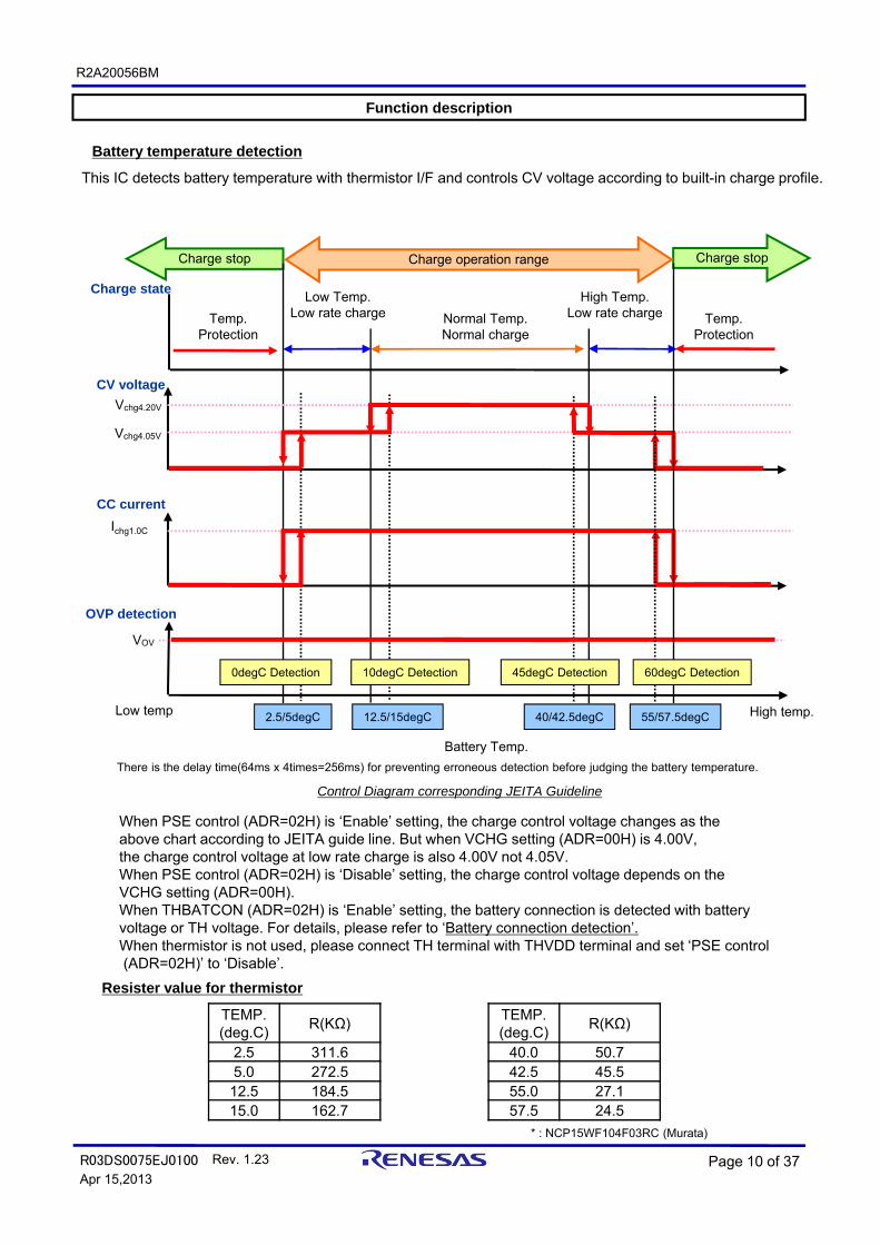
Battery temperature detection
Charge stopCharge stop
2.5/5degC
Normal Temp.Normal charge
High temp.Low temp
CV voltage
CC current
Vchg4.20V
Ichg1.0C
40/42.5degC
Vchg4.05V
OVP detection
VOV
12.5/15degC
Low Temp.Low rate charge
55/57.5degC
Temp.Protection
Temp.Protection
Charge operation range
Charge state
Battery Temp.
High Temp.Low rate charge
This IC detects battery temperature with thermistor I/F and controls CV voltage according to built-in charge profile.
There is the delay time(64ms x 4times=256ms) for preventing erroneous detection before judging the battery temperature.
When PSE control (ADR=02H) is ‘Enable’ setting, the charge control voltage changes as the above chart according to JEITA guide line. But when VCHG setting (ADR=00H) is 4.00V, the charge control voltage at low rate charge is also 4.00V not 4.05V.When PSE control (ADR=02H) is ‘Disable’ setting, the charge control voltage depends on the VCHG setting (ADR=00H). When THBATCON (ADR=02H) is ‘Enable’ setting, the battery connection is detected with batteryvoltage or TH voltage. For details, please refer to ‘Battery connection detection’.When thermistor is not used, please connect TH terminal with THVDD terminal and set ‘PSE control (ADR=02H)’ to ‘Disable’.
Resister value for thermistor
Function description
TEMP.(deg.C)
R(KΩ)
2.5 311.6 5.0 272.5 12.5 184.5 15.0 162.7
TEMP.(deg.C)
R(KΩ)
40.0 50.7 42.5 45.5 55.0 27.1 57.5 24.5
0degC Detection 10degC Detection 45degC Detection 60degC Detection
Control Diagram corresponding JEITA Guideline

R2A20056BM
Apr 15,2013R03DS0075EJ0100 Rev. 1.23 Page 11 of 37
USB port detection
[ USB port detection flow chart ]
No
No
Yes
VIN>3.3V
VBAT > VSYSSWOFF
DP < VLGC_LOW
Dead BatteryProvision
Mode
Yes
DM > VDAT_REF
Yes
No
DCP
DP > VDAT_REF
Yes
No
Data ContactDetection
PrimaryDetection
SecondaryDetection
CDP SDP
YesDM >1.0V
Yes
700ms Timer Start
USB battery charging 1.2
Timer 700ms?DP>3.3V
No
VBAT > VSYSSWOFF
SUSPEND
SDP &Timer > Twchg
DM >1.0VYes
DPERROR
DM>3.3VDM
ERROR
DP>2.3V
VBUSDivided Port 3
DM>2.3VVBUS
Divided Port 2
VBUSDividedPort 1
No
Yes
Yes
Yes
Yes
No
No
No
No(VLGC_LOW : 0~0.8V)
(VDAT_REF : 0.25~0.4V)
Divided PortDetection
(DM : 200KohmPulled-down)
Divided PortDetection
(DM : 200KohmPulled-down)
Function description
TOUT_DCD: ‘1’
TOUT_WKB: ‘1’
This IC detects the type of USB port as the following chart after USB connection.

R2A20056BM
Apr 15,2013R03DS0075EJ0100 Rev. 1.23 Page 12 of 37
6 types of USB port detection are enabled by detecting DP and DM terminals and the current limit is automatically set for each port. This detection starts after applying the voltageabove VULVO (TYP. 3.3V) to IN terminal or sending reset signal by RST_USBDET (ADR:02H).
04H USB Detection result (Read only)
The detection result is stored in the registers.When DP and DM terminals are open, this IC regards the port as SDP and indicates ‘1’ in ‘TOUT_DCD’ register. When DP>3.3V or DM>3.3V, this IC indicates 'ERROR' register and enter the suspend mode.Suspend is can be dissolved by ‘RST_USBDET’ or ‘USBMD’.
*1 It depends on CTL terminal setting
For VBUS Divided Port, this IC detects the combination of the divided voltagewith ‘DP’ and ‘DM’ terminals as the following chart.
USB detection timing chartVIN
USB detection
SYS voltage
/POK
<- Attach
Detecting
max 1s
4ms
64ms
Battery voltage
DP and DM terminal become Hi-Z (open) after USB detection.
Function description
No. Port USB battery charging 1.2 Current limit (mA)
1 SDP (Standard Downstream Port) O 100 or 500 *1
2 CDP (Charging Downstream Port) O 1500
3 DCP (Dedicated Charging Port) O 1500
4 VBUS Divided Port 1 - 500
5 VBUS Divided Port 2 - 1000
6 VBUS Divided Port 3 - 1800
CTL SDP current limitLo 100mAHi 500mA
Bit5 Bit4 Bit3 USB0 0 0 SDP (Standard Downstream Port)0 0 1 CDP (Charging Downstream Port)0 1 0 DCP (Dedicated Charging Port)1 0 0 VBUS Divided Port 11 0 1 VBUS Divided Port 21 1 0 VBUS Divided Port 30 1 1 DP ERROR1 1 1 DM ERROR
Port DP DM Current limit(mA)
VBUS Divided Port 1 2.00V 2.00V 500
VBUS Divided Port 2 2.00V 2.68V 1000
VBUS Divided Port 3 2.68V 2.00V 1800
SYS control voltage
* These voltages are the divided voltage at VIN=5.0V. These voltages also change with VIN voltage at this dividing ratio.
* Please set the downside resistance of the divided resistances to be above 100Kohm.

R2A20056BM
Apr 15,2013R03DS0075EJ0100 Rev. 1.23 Page 13 of 37
Dead Battery Provision
When VBAT < Vsysswoff_set (low battery detection voltage) at the USB detection, the behaviors
for each USB port are as follows:
< SDP ( Standard Downstream Port) >
- SG terminal is ‘H’.
- Trickle charge or quick charge can start.
- Dead Battery Provision starts and DP terminal outputs VDP_SRC (Typ. 0.6V).
- If VBAT doesn’t exceed Vsysswoff in Twchg (typ. 40min.), it shifts into the suspend mode.
Please reconnect with VIN to resolve this suspend mode.
- It can stop Weak Battery timer to set Timer Control (ADR=01H) to ‘RESET’ or ‘Count Stop’.
Setting input current with ‘USBMD’=‘1’ can avoid shifting into the suspend mode.
- When VBAT > Vsysswon ( Vsysswoff + Vsysswoff_hys) , the USB detection is carried out again.
During the USB detection, it shifts into the suspend mode and SYS terminal outputs BAT voltage.
The charge function starts from ‘Default (00H)’ and SG terminal is ‘L’. DP and DM terminals
becomes Hi-Z (open) after the USB detection.
If the battery voltage drops below Vsysswoff after this, Dead Battery Provision doesn’t start again.
/SG is set to ‘H’ but Weak Battery timer and VDP_SRC output from DP terminal don’t operate.
< DCP ( Dedicated charging Port) >
- SG terminal is ‘H’.
- Trickle charge or quick charge can start.
- Dead Battery Provision starts and DP terminal outputs VDP_SRC (Typ. 0.6V).
- Weak Battery timer (Typ. 40 min) doesn’t count up. But the each charging timer
(trickle or quick charge timer) counts up.
- When VBAT > Vsysswon ( Vsysswoff + Vsysswoff_hys) , the USB detection is carried out again.
During USB detection, it shifts into the suspend mode and SYS terminal outputs BAT voltage.
The charge function starts from ‘Default (00H)’ and SG terminal is ‘L’. DP and DM terminals
becomes Hi-Z (open) after the USB detection.
If the battery voltage drops below Vsysswoff after this, Dead Battery Provision doesn’t start again.
/SG is set to ‘H’ but VDP_SRC output from DP terminal doesn’t operate.
< CDP ( Charging Downstream Port) >
- the operation is the same as DCP. But during Dead Battery Provision mode, this port is detected
as ‘DCP’ and USB detection register (ADR=04H) also indicates ‘DCP’.
< Divided port 1,2,3>
- There isn’t Dead Battery Provision for Divided port. USB detection after good battery detection
doesn’t start.
- SG terminal is ‘H’.
Connecting IN terminal when BAT is open is regarded as ‘Weak Battery’ and Dead Battery
Provision starts. If Dead Battery Provision continues in Twchg, it shifts into the suspend mode.
For avoiding shifting into the suspend mode, set timer control (ADR=01H) to ‘RESER’ or
‘Count STOP’.
Function description

R2A20056BM
Apr 15,2013R03DS0075EJ0100 Rev. 1.23 Page 14 of 37
This function controls ‘/SG’ terminal.‘/SG’ terminal is connected with the LoadSW (recommended Renesas HAT1069C) betweenThe SYS terminal and SYSTEM, and controls power supply to SYSTEM ON/OFF.And ‘/SG’ terminal can be used for the control of an USB SW because this terminal becomes ‘H’ (OFF) during the USB detection.
1. ‘/SG’ = ‘H’ (‘OFF’) during the USB detection or Dead Battery Provision. ‘H’ voltage during the USB detection can become the BAT voltage. Refer to ‘Starting function after IN connected’.
2. This function can be selected for ‘Enable’ or ‘Disable’ by SGCTL (ADR=02H).3. When the battery voltage is low, all current can be used for charging by stopping the current
supply for SYSTEM with the LoadSW off. (After USB detection & SGCTL: Enable)
[/SG control in each condition about the IN and the BAT ( Except for the USB detection,Dead Battery Provision and SGCTL: Disable)]
(1) IN : connect , BAT : connectVBAT < Vstart ON(‘L’) Vstart < VBAT <VSYSSWOFF OFF(‘H’) VSYSSWOFF < VBAT ON(‘L’)
(2) IN : connect , BAT : non-connect ON(‘L’) (3) IN : non-connect , BAT : connect ON(‘L’) (4) IN : non-connect , BAT : non-connect IC and SYSTEM are not operated
Timing of /SG output
/POK
Vsysswoff
64ms
Vsysswoff,hys
VBAT
/SG 64ms
LoadSW ON LoadSW OFF LoadSW ON
Gate control for system Load SW (/SG)
When SGCTL=0(enable)
‘L’ setting ‘H’ setting
Function description
Vsysswon
SGREF terminal setup
The low battery detection voltage (Vsysswoff) is used for the following functions. - Detection weak battery after ‘Forced charge (01H)’ - On/off function for MOSFET for System load SW’
SGREF terminal voltage (VSGREF) can set the low battery detection voltage(Vsysswoff).
[ SGREF detection voltage (Typ. 1.8V) < VSGREF ]- The internal setting is selected.
Vsysswoff = Vsysswoff_in (Typ. 3.4V) , Hysteresis voltage = Vsyssw_in_hys (Typ. 100mV)We recommend that SGREF is connected with THVDD when using the internal setting.
[ GND < VSGREF < SGREF detection voltage (Typ. 1.8V) ]- Vsysswoff = Vsysswoff_out
Relational expressions are as follows:VSGREF = 0.354 x Vsysswoff_out
Vsyssw_out_hys = 200mV x Vsysswoff_out / 3.4V
* Input 0.3V to SGREF if the low battery detection function is not used.It is possible to divide THVDD voltage with upper 51KΩ and lower 9.1KΩ resistances .
SYS ControlVoltage

R2A20056BM
Apr 15,2013R03DS0075EJ0100 Rev. 1.23 Page 15 of 37
Input current limitation / Control between SYS and BAT
- USB detection (USB battery charging 1.2)- Input current limitation(100mA/500mA/1000mA/1500mA/1800mA/limitless/Suspend) can be set by I2C.-The current limit is dropped as the list for protection when SYS is shorted.-When the total sum of the charge current and the system current is below the input limit current,
SYS terminal outputs IN voltage directly. When IN voltage is over 5.4V, SYS voltage is controlled to be below 5.4V.Capable for switching between VSYS45 and VIN pass-through by I2C.
-IC switches the system power supply and the battery charge seamlessly within input current limitation.
System
USBIN
SYS
BAT
ISYS
Ichg
IbatVBAT
VSYSIin
CC/CV/SYScontrol
SYS_RegCurrent Limit
/SG
SYS SWGate
Control
Example of power control between the system supply and the battery chargeConditions : IN=5.0V is connected, Iin_max=500mA, Ichg=350mA, Chargeable battery is connected.
(1)
(2)
(3)
The IC charges the battery at Ichg=350mA and supplies the system current(ISYS) within Iin_max=500mA.
When the system current(ISYS) increases and the total sum of ISYS and Ichg reaches Iin_max,the IC reduces the charge current.
When the system current (ISYS) increases more and ISYS exceeds Iin_max,VSYS falls to VBAT-VSYSR and the battery supplies the load current to system through the Path SW. (IC attempts to sustain the system voltage no matter what causes it to drop.)
Time
Current
0mA
350mA
Input voltage
VBAT-VSYSR
Input current
(Iin)
Iin_max
Time
VSYS
VSYS43
(2)(1) (3)
Battery to systemcurrent(IBAT)
VBAT
Systemcurrent(ISYS)
Chargecurrent(Ichg)
VIN pass-through or VSYS45
Current Limit
Settingat SYS short
100mA
500mA20%
1000mA 40%
1500mA
1800mA50%
( Design Guarantee)
Function description
Input Current Limit when SYS is shorted.
Auto load current distribution control

R2A20056BM
Apr 15,2013R03DS0075EJ0100 Rev. 1.23 Page 16 of 37
VIN
VUVLO
VInBat
VOVP
tDGLH(/POK)
/POK
VOVPHys
VInBatHys
VUVLOHys
tDGLH(OVP) tDGLL(OVP) tDGLL(/POK)32µs 64ms 64ms
USB detection64ms
Detection
Max 1s
Over load detection
Input voltage detection
/POK timing chart
VIN voltage rangeduring normal operation
Operation of Over load detection
VIN
SYS
ISYS
OVERLOAD
(ADR:03H Bit0)
VHL Control (VIN)
BAT
BAT-VSYSR Control
'0' '0' '1'
Overload
(Current Capability < Current Limit)
Function description
When IN voltage drops below VHL, the input current is controlled as the current at the timeregardless of the current limit setting. The OVERLOAD register (ADR:03H Bit0) indicate '1'.
This IC detects lack of current capability of power supply and prevents exceeded current from flowing from IN terminal.
VUVLO<VIN<VOVP and VIN>VBAT+VInBat : Power supply from IN to SYS and charging are available. /POK =L.
VOVP<VIN or the suspend mode : Power supply from IN to SYS and charging are not available. /POK=H.
* This detection operates when IN voltage < VHL.In this mode, charging doesn’t operate.
The suspend mode is shifted at the following situation:- USUP : ’H’ - I2C setting (CTL3) - USB detection- Weak Battery Timer : Time out- DP ERROR or DM ERROR (After USB detection)- USB detection reset (RST_USBDET : Enable)

R2A20056BM
Apr 15,2013R03DS0075EJ0100 Rev. 1.23 Page 17 of 37
connection sequence
Battery
condition
Thermistor
Included in battery *1 on board *2 No use *3
BAT -> IN
NormalStarting from
Default(00H)
Starting from
Default(00H)
Starting from
Default(00H)
Open BatteryStarting from
Default(00H)
Starting from
Default(00H)
Starting from
Default(00H)
IN -> BAT*4
NormalStarting from
Default(00H)Forbidden
Open Battery Default(00H)
connection sequence
Battery
condition
Thermistor
Included in battery *1 On board No use
BAT -> IN
NormalStarting from
Default(00H)
Forbidden
Open BatteryStarting from
Default(00H)
IN -> BAT*4
NormalStarting from
Default(00H)
Open BatteryStarting from
Default(00H)
THBATCON : ‘Disable’
THBATCON : ‘Enable’
*1 : TH voltage is in the charging range.Charging doesn’t starts with no battery because TH voltage is not in the charging range.
*2 : TH voltage is in the charging range. *3 : PSE Control : ‘Disable’ *4 : Don’t start charging with no battery.
Function description
Battery connection detection

R2A20056BM
Apr 15,2013R03DS0075EJ0100 Rev. 1.23 Page 18 of 37
Battery connection is detected by battery voltage as follows:
- Battery voltage (VBAT) > Charge start voltage (Vstart)
When register [ THBATCON (ADR:02H) ] is set to ‘Enable’, Battery connection isdetected by battery voltage or TH terminal voltage as follows:
- Battery voltage (VBAT) > Charge start voltage (Vstart)- TH terminal voltage < Thermistor connection detect voltage (VTHCON)
When thermistor is included in battery pack and this register is set to ‘Enable’, chargingcan also starts for an open battery.When thermistor isn’t included in battery pack, please don’t set this register ‘Enable’.
The list in the previous page shows the behavior with 3 kinds of thermistor setting and 2 kinds of battery.
<Thermistor> ‘Included in battery’ , ‘On board’ , ‘No use’ <Battery> ‘Normal’ , ‘Open battery’
When THBATCON(ADR:02H) is ‘Disable’ setting (Default setting) , the battery connectionis detected by only battery voltage. When IN is connected after ‘battery connection’, charging starts from ‘Default (00H)’ statefor both ‘Normal’ and ’Open battery ‘. When IN is connected before ‘battery connection’, charging starts for ‘Normal’ batteryas same as when IN is connected after ‘battery connection’. For ’Open battery ‘,the state stays at ‘default(00H)’ because it can’t detect battery connection. And charging is forbidden with no battery when thermistor is ‘On board’ or ‘No use’.
If THBATCON (ADR:02H) is set to ‘Enable’, battery connection is detected by either batteryvoltage or TH terminal voltage. Charging also starts for ’Open battery’ as same as ‘Normal’.So it is possible to charge for all batteries when thermistor is ‘Included in battery’. When thermistor is ‘On board’ or ‘No use’, THBATCON (ADR:02H) ‘Enable’ setting is forbidden. And please don’t charge with no battery.
Function description

R2A20056BM
Apr 15,2013R03DS0075EJ0100 Rev. 1.23 Page 19 of 37
/SG
BAT
VSYS
(1) USB detection with Good Battery (VBAT>VSYSSWOFF) after IN connected
Vuvlo
VIN
SYS
BAT voltage
USB Detection Normal Charge
LoadSW ON LoadSW OFF LoadSW ON
/POK
I2C
4ms
64ms
SYS control voltage (VIN pass-through or VSYS45)
(1) USB detection with Good Battery (VBAT>VSYSSWOFF) after IN connected
(2) USB detection with Weak Battery (VBAT<VSYSSWOFF) after IN connected
[Battery Charging 1.2 Port]
(3) USB detection with Weak Battery after IN connected [Divided Port]
(4) USB detection with no Battery after IN connected [Battery Charging 1.2 Port]
(5) USB detection with no Battery after IN connected [Divided Port]
Starting function after IN connected
We show starting function for each battery and USB port.
/POK : VSYS pulled-up
EnableDisable
Function description

R2A20056BM
Apr 15,2013R03DS0075EJ0100 Rev. 1.23 Page 20 of 37
(2) USB detection with Weak Battery (VBAT<VSYSSWOFF) after IN connected
[Battery Charging 1.2 Port]
Function description
BAT Voltage
/SG
BAT
100ms
VSYS
Vsysswon
BAT
SYS
Dead Battery Provision
LoadSW ON LoadSW OFF LoadSW OFF
Vuvlo
VIN
LoadSW ON
Normal Charge
/POK
I2C
EnableDisable
4ms
64ms
64ms
OPEN after USB Re-detectionVDP_SRCDP OPEN
SYS Control Voltage
SYS Control Voltage
USBRe-detection
The condition of DP changesduring USB re-detection.
64ms 64ms
USB Detection
BAT voltage
* Weak battery timer operates during Dead Battery Provision at SDP. If the battery voltage doesn’t exceed Vsysswoff in Twchg (typ. 40min.), it shifts into the suspend mode. (Refer to ‘Dead Battery Provision’.)

R2A20056BM
Apr 15,2013R03DS0075EJ0100 Rev. 1.23 Page 21 of 37
BAT voltage
/SG
BAT
100ms
VSYS
Vsysswon
BAT
SYS
LoadSW ON LoadSW OFF LoadSW OFF
Vuvlo
VIN
LoadSW ON
Normal charging* Dead Battery Provision doesn’t start for Divided port.
/POK
I2C
EnableDisable
4ms
64ms
64ms
SYS Control Voltage
SYS Control Voltage
USB detection
Function description
(3) USB detection with Weak Battery (VBAT<VSYSSWOFF) after IN connected
[Divided Port]

R2A20056BM
Apr 15,2013R03DS0075EJ0100 Rev. 1.23 Page 22 of 37
/SG
100ms
VSYS
Vsysswon
BAT
SYS
Dead Battery Provision
LoadSW ON LoadSW OFF
Vuvlo
VIN
LoadSW ON
Normal Charge
/POK
I2C
EnableDisable
4ms
64ms
64ms
OPEN after USB detectionVDP_SRCDP OPEN
SYS Control Voltage
SYS Control Voltage
USBRe-detection
The condition of DP changesduring USB re-detection.
64ms 64ms
USB Detection
BAT
Battery Connection
BAT VoltageBAT Voltage
0V
Function description
(4) USB detection with no Battery after IN connected
[Battery Charging 1.2 Port]
* Weak battery timer operates during Dead Battery Provision at SDP. If the battery voltage doesn’t exceed Vsysswoff in Twchg (typ. 40min.), it shifts into the suspend mode. (Refer to ‘Dead Battery Provision’.)
* Dead Battery Provision lasts when a weak battery is connected.USB re-detection starts when the battery becomes a good battery.
* Please start charging after connecting a battery. Don’t start charging with no battery.

R2A20056BM
Apr 15,2013R03DS0075EJ0100 Rev. 1.23 Page 23 of 37
/SG
100ms
VSYS
Vsysswon
BAT
SYS
LoadSW ON LoadSW OFF
Vuvlo
VIN
LoadSW ON
Normal charging* Dead Battery Provision doesn’t start for Divided port.
/POK
I2C
EnableDisable
4ms
64ms
64ms
SYS Control Voltage
SYS Control Voltage
USB detection
Battery Connection
BAT Voltage0V
Function description
(5) USB detection with no Battery after IN connected
[Divided Port]
* /SG doesn’t change when a weak battery is connected./SG becomes ‘L’ after the battery becomes a good battery.
* Please start charging after connecting a battery. Don’t start charging with no battery.

R2A20056BM
Apr 15,2013R03DS0075EJ0100 Rev. 1.23 Page 24 of 37
Forced charge
Trickle charge current or Quick charge current
Chargecurrent
/STAT (LED)
Input connection
1256ms max
Input connectiondetection
Forced charge ON
Forced charge current
640ms
Battery voltage detection
OFF ON
Forced charge mode
Timing from input detection to charge start
Trickle charge or Quick charge mode
(0.1C)
(0.2C)
0.1C or 0.2CSelectableby register
256ms
After input power detection, forced charge starts for canceling the cutoff state of battery due to over-discharge.The forced charged current is the same as trickle charge current setting. Register ( ADR=00H Bit6) is availablefor changing setting.Charging starts even with an open battery by this function.Please refer to Battery connection detection.
Trickle charge (0.1C constant current charge)
After input detection and battery detection, trickle charge starts when VBAT < Vqcchgon (Typ. 3.0V).
- When detecting VBAT > Vqcchgon , the state shifts to quick charge mode.
- Trickle charge timer starts when trickle charge starts.
- After trickle charge timer expires, the state shifts to ‘error mode 1’ if VBAT < Vqcchgon .However trickle timer stops when the battery voltage becomes below Vstart. When BATis shorted, this timer also stops. NOBAT(ADR=03H, Bit5) indicates detecting the battery voltage below Vstart. After NOBAT=‘1’ by detecting VBAT < Vstart, please stop charging with /CEN.
- When detecting VBAT > Vov (Typ. 4.35V), the state shifts to ‘error mode 1’.
Trickle charge setting is selectable between 0.1C and 0.2C by register (ADR=00H Bit4,5).
Quick charge (1.0C constant current charge)
Quick charge starts after detecting VBAT > Vqcchgon.
- When detecting VBAT=Vchg, the state shifts to CV (constant voltage) charge mode.
- Quick charge timer starts when quick charge starts.
- When detecting VBAT < (Vchgon – hysteresis voltage) (Typ. 2.9V) , the state shifts to trickle charge mode.
- When detecting VBAT > Vov (Typ. 4.35V), the state shifts to ‘error mode 1’.
During quick charge, this IC monitors junction temperature and controls the current between 0.2C and 1.0C
not to exceed Ttreg.
The quick charge current is selectable between 0.5C and 1.0C by register (ADR=00H Bit 0).
Function description
Battery Temp.detection

R2A20056BM
Apr 15,2013R03DS0075EJ0100 Rev. 1.23 Page 25 of 37
Quick Chargemode
Timing to Quick charge(1.0C)
Chargecurrent
Batteryvoltage
Quick Chargecurrent (0.2C)
Quick charge current(1.0C)
(7.68sec) (24.58sec)256ms
TrickleChargecurrent(0.1C)
Trickle Chargemode
Quick chargeStart voltagedetection
Vqcchgon
256ms
Charge completioncurrent detection
384ms
256ms
Battery voltage detection
VBAT terminal discharge
(about 200µA)
Charge completion detection
Timing of charge completion detection
Chargecurrent
Batteryvoltage
Charge completion(07H)
Constant voltage charge
When detecting VBAT=Charge Control voltage during quick charge mode, constant voltage charge starts.- When the charge current falls below charge completion current during constant voltage charge, the state shifts to charge completion detection mode. If VBAT>Vrechg (Typ. 3.8V), the state shifts to charge completionstate.
- When Vstart < VBAT < Vrechg, the state shifts to ‘error mode 1’.- When VBAT < Vstart, the state shifts to Battery non-connection mode.- The current (about 200µA) is discharged from BAT terminal during the charge completion detection mode.
After this state, the next state is selected among Charge completion, Battery non-connection orError-1 by the battery voltage.
- The charge control voltage is selectable from 4.00V to 4.20V (50mV steps) by register (ADR=00H Bit 1,2,3).
Charge completion detection state(06H)
Function description
R2A20056BM
Apr 15,2013R03DS0075EJ0100 Rev. 1.23 Page 26 of 37
256ms
Battery voltage detection
Recharge detection
Timing of recharge judgment
Quick charge mode
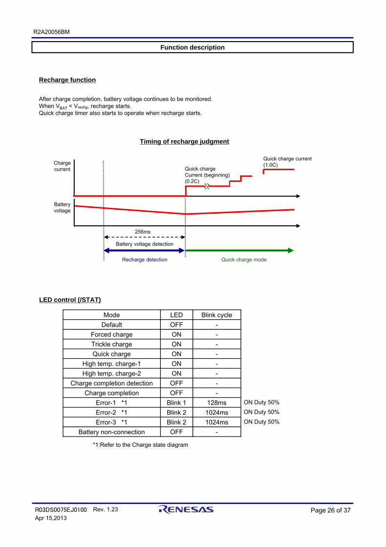
Recharge function
After charge completion, battery voltage continues to be monitored.When VBAT < Vrechg, recharge starts.Quick charge timer also starts to operate when recharge starts.
Chargecurrent
Batteryvoltage
Quick chargeCurrent (beginning)(0.2C)
Quick charge current(1.0C)
LED control (/STAT)
*1:Refer to the Charge state diagram
ON Duty 50%
ON Duty 50%
ON Duty 50%
Function description
Mode LED Blink cycle
Default OFF -
Forced charge ON -
Trickle charge ON -
Quick charge ON -
High temp. charge-1 ON -
High temp. charge-2 ON -
Charge completion detection OFF -
Charge completion OFF -
Error-1 *1 Blink 1 128ms
Error-2 *1 Blink 2 1024ms
Error-3 *1 Blink 2 1024ms
Battery non-connection OFF -

R2A20056BM
Apr 15,2013R03DS0075EJ0100 Rev. 1.23 Page 27 of 37
Charge Current Setting
[ Design guarantee except for Ichg=500mA ]
Accuracy of each setting about charge current and charge completion current
Charge Current is set by the external resistance with RICHG terminal.Here is the formula between RICHG and Ichg1.0C.
RICHG = 812 x Ichg1.0C-0.9 RICHG (Kohm) : External Resistance with RICHG
Ichg1.0C (mA) : Quick charge setting
0.2C, 0.1C and 0.05C are 20%, 10% and 5% current of 1.0C.They can be set by register ( ADR=00H).
The accuracy of each current is as the following list.Please use the current over 5mA.
Ichg1.0C Iprechg0.2C , Iprechg0.1C Ifc0.2C , Ifc0.1C Ifc0.05C
Charge Current (mA)Charge Completion
Current (mA)
Acc
ura
cy(%
)
ItemQuick Charge Current(Ichg1.0C) Setting
500mA<Ichg1.0C Ichg1.0C=500mA 50mA<Ichg1.0C<500mA
Ichg1.0C +-[10+(Ichg1.0C-500mA)/100mA] [%] +-10[%] +-[30+(50mA-Ichg1.0C)/22.5mA] [%]
Iprechg0.2C +-[30+(Ichg1.0C-500mA)/100mA] [%] +-30[%] +-[40+(50mA-Ichg1.0C)/45mA] [%]
Iprechg0.1C +-[30+(Ichg1.0C-500mA)/100mA] [%] +- 30[%] +-[40+(50mA-Ichg1.0C)/45mA] [%]
Ifc0.2C +-[30+(Ichg1.0C-500mA)/100mA] [%] +- 30[%] +-[50+(50mA-Ichg1.0C)/22.5mA] [%]
Ifc0.1C +-[30+(Ichg1.0C-500mA)/100mA] [%] +- 30[%] +-[50+(50mA-Ichg1.0C)/22.5mA] [%]
Ifc0.05C +-[40+(Ichg1.0C-500mA)/100mA] [%] +- 40[%] +-[50+(50mA-Ichg1.0C)/45mA] [%]
Ichg1.0C[mA] - RICHG[Kohm]
0.0
2.0
4.0
6.0
8.0
10.0
12.0
14.0
0 200 400 600 800 1000 1200 1400 1600
Ichg1.0C [mA]
RIC
HG [K
ohm
]
Charge Current (mA)Charge Completion
Current (mA)
0
10
20
30
40
50
0 500 1000
0
10
20
30
40
50
0 50 100
0
10
20
30
40
50
0 50 100
0
10
20
30
40
50
0 25 50
Function description

R2A20056BM
Apr 15,2013R03DS0075EJ0100 Rev. 1.23 Page 28 of 37
Chip temperature detection and Thermal shutdown
Ichg(A)
Battery voltage (V)
1.0C/0.5C
JunctionTemperature(degC)
(110degC)
(100degC)
Ichg(mA)
0.2C
(125degC)
Increase of Ichg is stopped and Tj falls.
When Tj<Ttreg_down,IC re-starts increasing Ichg.
Tj rises at Ttrgrst by change of ambient temperature.
(150degC)
When Tj>Ttrgrst, Ichg is set at 0.2C by the chip temperature reset detection.
Tj rises at Tsd by abnormal situation.
Charging operation stops by thermal shutdown.
Quick charge starts.
Chip temperature detection
Thermal shutdown
During quick charge, junction temperature is monitored to limit charge current between 0.2C to 1.0C so that junction
temperature may not exceed Ttreg.
When junction temperature reaches Tsd( default: 150degC) under charge, IC stops to supply from IN to SYS
and the state moves to error mode.
When Tj>Ttreg,IC stops increasing Ichg.
When Ichg reaches 1.0C (regulated value),IC stops to increase Ichg.
Tsd
Ttrgrst
Ttreg
Ttreg_down
(Ttreg -hysteresis voltage)
Function description

R2A20056BM
Apr 15,2013R03DS0075EJ0100 Rev. 1.23 Page 29 of 37
03H State register (Read only)
05H State register (Read only)
05H<4> ~ <7> Keep 0When charge FULL, FULL=0 and TOUT=0.When Suspend, TSD=0,TOUT=0,FULL=0,VBATH=0,NOBAT=1.
04H TEMP register (Read only)
04H USB detection result (Read only)
Register Map
ADR Bit7 Bit6 Bit5 Bit4 Bit3 Bit2 Bit1 Bit000H R/W - TRICKLE FC VCHG ICHG01H R/W USBMD TIMER CTL3 /CEN202H R/W SYSMODE RST_USBDET THBATCON SGCTL FULMD RECHG PSE03H R GDBAT VBATH NOBAT FULL TOUT TSD POK OVERLOAD
04H R TOUT_WKB TOUT_DCD USB TEMP05H R 0 0 0 0 STAT3 STAT2 STAT1 STAT0
0 1 Condition of ‘1’OVERLOAD Not Overload Overload VIN < VHL
POK Not Detect VIN Detect VIN /POK=‘L’TSD IC chip temperature is Normal Thermal protection work (IC stop) Tj > Tsd
TOUT Timer normal Time out (Charging stop)Timeout of Trickle or Quick Charge timer
FULL Charging not complete Charging complete Ichg < Ifc (During CV)NOBAT Battery detected No Battery VBAT < Vstart
VBATH Battery voltage normal Battery over voltage VBAT > VOV
GDBAT Weak Battery Good Battery VSYSSWOFF < VBAT
Bit2 Bit1 Bit0 TEMP0 0 0 Temperature protection (Low Temp.)0 0 1 Low rate charge (Low Temp.)0 1 0 Normal charge0 1 1 Low rate charge (High temp.)1 0 0 Temperature protection (High temp.)1 0 1 No Thermistor
Bit5 Bit4 Bit3 USB0 0 0 SDP (Standard Downstream Port)0 0 1 CDP (Charging Downstream Port)0 1 0 DCP (Dedicated Charging Port)1 0 0 Divided Port 11 0 1 Divided Port 21 1 0 Divided Port 30 1 1 DP ERROR1 1 1 DM ERROR
Bit7 Weak Battery Timer0 Normal1 Time out
STAT3 STAT2 STAT1 STAT0 State0 0 0 0 Default0 0 0 1 Forced charge0 0 1 0 Trickle charge0 0 1 1 Quick charge0 1 0 0 High temp. charge-10 1 0 1 High temp. charge-20 1 1 0 Charge completion detection0 1 1 1 Charge completion1 0 0 0 Battery non-connection1 0 0 1 Error-11 0 1 0 Error-21 0 1 1 Error-3
Bit6 Connect Detection0 Normal1 Time out
04H TOUT_WKB register (Read only)
04H TOUT_DCD register (Read only)
R2A20056BM
Apr 15,2013R03DS0075EJ0100 Rev. 1.23 Page 30 of 37
*Default setting
Register setting
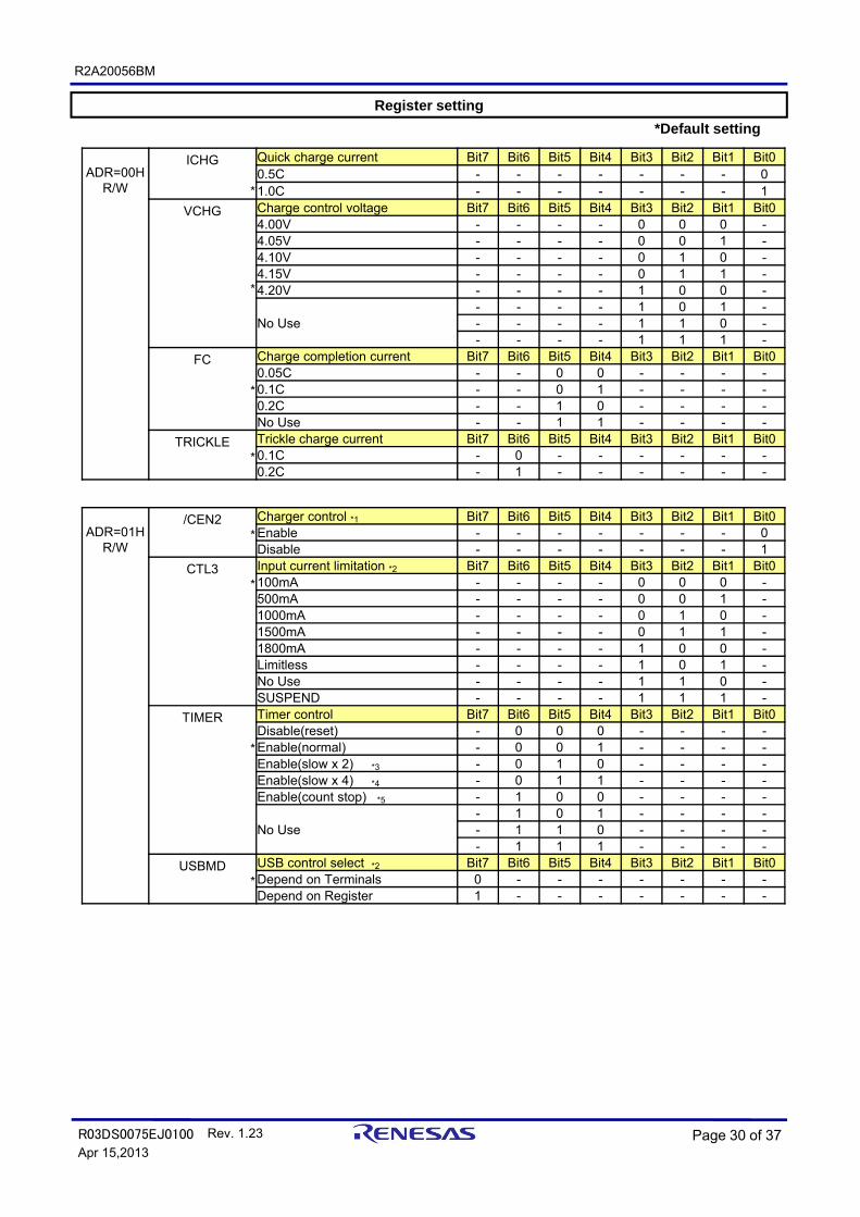
ADR=00H R/W
ICHG
*
Quick charge current Bit7 Bit6 Bit5 Bit4 Bit3 Bit2 Bit1 Bit00.5C - - - - - - - 01.0C - - - - - - - 1
VCHG
*
Charge control voltage Bit7 Bit6 Bit5 Bit4 Bit3 Bit2 Bit1 Bit04.00V - - - - 0 0 0 -4.05V - - - - 0 0 1 -4.10V - - - - 0 1 0 -4.15V - - - - 0 1 1 -4.20V - - - - 1 0 0 -
No Use- - - - 1 0 1 -- - - - 1 1 0 -- - - - 1 1 1 -
FC
*
Charge completion current Bit7 Bit6 Bit5 Bit4 Bit3 Bit2 Bit1 Bit00.05C - - 0 0 - - - -0.1C - - 0 1 - - - -0.2C - - 1 0 - - - -No Use - - 1 1 - - - -
TRICKLE *
Trickle charge current Bit7 Bit6 Bit5 Bit4 Bit3 Bit2 Bit1 Bit00.1C - 0 - - - - - -0.2C - 1 - - - - - -
ADR=01H R/W
/CEN2 *
Charger control *1 Bit7 Bit6 Bit5 Bit4 Bit3 Bit2 Bit1 Bit0Enable - - - - - - - 0Disable - - - - - - - 1
CTL3*
Input current limitation *2 Bit7 Bit6 Bit5 Bit4 Bit3 Bit2 Bit1 Bit0100mA - - - - 0 0 0 -500mA - - - - 0 0 1 -1000mA - - - - 0 1 0 -1500mA - - - - 0 1 1 -1800mA - - - - 1 0 0 -Limitless - - - - 1 0 1 -No Use - - - - 1 1 0 -SUSPEND - - - - 1 1 1 -
TIMER
*
Timer control Bit7 Bit6 Bit5 Bit4 Bit3 Bit2 Bit1 Bit0Disable(reset) - 0 0 0 - - - -Enable(normal) - 0 0 1 - - - -Enable(slow x 2) *3 - 0 1 0 - - - -Enable(slow x 4) *4 - 0 1 1 - - - -Enable(count stop) *5 - 1 0 0 - - - -
No Use- 1 0 1 - - - -- 1 1 0 - - - -- 1 1 1 - - - -
USBMD *
USB control select *2 Bit7 Bit6 Bit5 Bit4 Bit3 Bit2 Bit1 Bit0Depend on Terminals 0 - - - - - - -Depend on Register 1 - - - - - - -

R2A20056BM
Apr 15,2013R03DS0075EJ0100 Rev. 1.23 Page 31 of 37
*2) When USBMD=0, Terminal setting(USUP) is available. When USBMD=1, Register(CTL3) is availableand the suspend function by Weak battery timer is unavailable.Re-connect with IN when going into the suspend mode by Weak battery timer.
*3) Slow: 2 times of normal mode(Trickle charge timer=120min., Quick charge timer=600min , Weak battery timer = 80min.)
*4) Slow: 4 times of normal mode(Trickle charge timer=240min., Quick charge timer=1200min , Weak battery timer = 160min.)
*5) Count stop : Timer is suspended.(Not reset)
*6) When RST_USB=1, the USB detecting is in reset and /SG output is 'L'. When RST_USB=0, the USB detecting will restart. During the USB detection, /SG is 'H'. After USB detection, /SG output is determined by the SG function.USB re-detection by RST_USBDET can reset the suspend by USB detecting error.
*7) The SYS voltage setting can be set by the SYSMODE register.
* When VIN<2.0V, the register is reset. (This value is design guarantee).
*1) When /CEN=L and /CEN2(register)='0', Charge operation is enable.
[Truth Table]
Register setting
ADR=02HR/W
PSE *
PSE control Bit7 Bit6 Bit5 Bit4 Bit3 Bit2 Bit1 Bit0Enable - - - - - - - 0Disable - - - - - - - 1
RECHG *
Recharge control Bit7 Bit6 Bit5 Bit4 Bit3 Bit2 Bit1 Bit0Enable - - - - - - 0 -Disable - - - - - - 1 -
FULMD*
Operation after charge completion Bit7 Bit6 Bit5 Bit4 Bit3 Bit2 Bit1 Bit0Stop charge - - - - - 0 - -Continue to charge(inform FULL) - - - - - 1 - -
SGCTL*
/SG control Bit7 Bit6 Bit5 Bit4 Bit3 Bit2 Bit1 Bit0Enable - - - - 0 - - -Disable - - - - 1 - - -
THBATCON*
Battery detection by TH terminal Bit7 Bit6 Bit5 Bit4 Bit3 Bit2 Bit1 Bit0Disable - - - 0 - - - -Enable - - - 1 - - - -
RST_USBDET*
USB detection reset Bit7 Bit6 Bit5 Bit4 Bit3 Bit2 Bit1 Bit0Disable - - 0 - - - - -Enable (Reset) - - 1 - - - - -
SYSMODE*
SYS Output MODE *1 Bit7 Bit6 Bit5 Bit4 Bit3 Bit2 Bit1 Bit0
VIN pass-through0 0 - - - - - -0 1 - - - - - -
VSYS45 (Typ. 4.5V) 1 0 - - - - - -VIN pass-through 1 1 - - - - - -
/CEN /CEN2 Charge OperationLo 0 Charge startLo 1 Charge stopHi 0 Charge stopHi 1 Charge stop

R2A20056BM
Apr 15,2013R03DS0075EJ0100 Rev. 1.23 Page 32 of 37
I2C Timing Chart
SDA
VIH
VIL
SCL
VIH
VIL
Start Start StartStop
tR, tFtBUF
tHD:STA tSU:DAT tHD:DAT tSU:STO
tLOW
tSU:STA
tHIGH
Symbol Item Min. Max. Unit
fSCL SCL clock frequency 0 400 kHz
tBUF Bus free time between STOP condition and START condition 1.3 - µs
tHD:STASTART condition hold time(After this period, the first clock pulse is generated)
0.6 - µs
tLOW SCL low period 1.3 - µs
tHIGH SCL high period 0.6 - µs
tSU:STA START condition setup time 0.6 - µs
tHD:DAT Data hold time 0 0.9 µs
tSU:DAT Data setup time 100 - ns
tR Rise time (SDA and SCL) - 300 ns
tF Fall time (SDA and SCL) - 300 ns
tSU:STO STOP condition setup time 0.6 - µs
Cb Bus line capacitive load - 400 pF
Note : Above values are specified by VIHmin and VILmax.
I2C BUS Line Characteristics

R2A20056BM
Apr 15,2013R03DS0075EJ0100 Rev. 1.23 Page 33 of 37
(Solid line: From Master to R2A20056, Dotted line: From R2A20056 to Master)
SDA
SCL
* * * * * * * ACK X X X X X A2 A1 A0 ACK D7 D6 D5 D4 D3 D2 D1 D0 ACKW
Register address(sub-address)
Write dataSlave addressStartcondition
Stopcondition
1. Start condition
LASTFIRSTLSBMSB
2. Slave address
0 0 1 1 0 1 1
3. Stop condition
SDA
SCL
Startcondition
* * * * * * * ACK X X A1 A0 ACKW
Register address(sub-address)
Slave address Read dataSlave addressStartcondition
Stopcondition
D7 D6 D5 D4 D3 D2 D1 D0 NACK* * * * * * * RACKX X X A2
5. Write mode :Data input from Master to R2A20056
Set SDA from High to Low when SCL=High.
Set SDA from Low to High when SCL=High.
Write code : SDA=LowRead code : SDA=High
(Solid line: From Master to R2A20056, Dotted line: From R2A20056 to Master)
6. Read mode :Data output from R2A20056 to Master
When Master inputs Slave address(8bit) and Write code after start condition, R2A20056 responds with an Acknowledge'0'. And then, when Master inputs Register address(8bit), R2A20056BM responds with an Acknowledge'0'. And then, when Master inputs Start condition, Slave address, and Read code, R2A20056 responds with an Acknowledge'0'and outputs Read data.Lastly, Master inputs Acknowledge'1'(or opens bus line) and Stop condition.
4. Read/Write code
Serial communication format
R2A20056 will respond with an Acknowledge ‘0’ when;- Master inputs Slave address (8bit) and Write code after start condition- Master inputs Register address (8bit)- Master inputs Write data (8bit)
Lastly, Master will input Stop condition.

R2A20056BM
Apr 15,2013R03DS0075EJ0100 Rev. 1.23 Page 34 of 37
[ The circuit around SDA, SCL terminals ]
< ‘H’ voltage >
dwnup
dwnpupH RR
RVV
dwnmosup
dwnmospupL RRR
RRVV
//
//
dwnmos RR
< ‘L’ voltage>
Please set the pull-up resistances to satisfy the calculating formula.
Vpup[V] : Pull-up voltage
Rup[KΩ] : Pull-up resistance
Rmos[KΩ] : ON resistance of NMOS in HOST
dwnup RR
ItemRated Value
UnitMin. Typ. Max.
pull-down Resistance of SCL,SDA 500 700 900 KΩ
[ Pull-down resistance with ‘SCL’ and ‘SDA’ terminals ]
[ I2C communication notice ]
SCL
SDA
The example of NG
SCL,SDA : ‘L’=> Miss-detecting as ‘START CONDITION’ No ‘ACK’
Serial communication format
Rdwn is affected lightly because of .
.Rdwn is affected lightly because of
There are pull-down resistances with ‘SCL’ and ‘SDA’ terminals in this IC.
Resending the command in the errorPlease resend the command when ACK is not returned normally.
Timing adjust when turning off the pull-up power supply Please make ‘SCL’ fall faster than ‘SDA’ when pull-up power is turned offwhile voltage is supplied to the IN terminal.
If ‘L’ signal is input to ‘SCL’ and ‘SDA’ terminals before normal I2C signal, this ICmay not accept this I2C signal because of detecting ‘Start condition’.When the pull-up voltage is turned off during continuing to supply voltage tothe IN terminal, the ‘L’ signal may be miss-detected as the start condition.Please take measures as follows:

R2A20056BM
Apr 15,2013R03DS0075EJ0100 Rev. 1.23 Page 35 of 37
4.7K~10Kohm
Typical Application Circuit
RICHG
Adaptor
USB
CTL
USUP
/CEN
System
BAT
SYS
TH
/STAT
/POK
GND
SYS
SYS
IN
SCL
SDA
HOST
/SG
DP DM
THVDD
SGREF
HAT1069C
USB SW
D-
D-D-
D-
D+D+ D+
D+
D- D+
THVDD
100Kohm
Thermistor (100Kohm)NCP15WF104F03RC
(MURATA)
4.7µF
4.7µF
10µF
Terminal Name Recommended Capacitance
IN 4.7~10µF
SYS 10µF
BAT 4.7~10µF
4.7K~10Kohm
R2A20056BM
Set the limit resistances
not to beyondthe absolute
maximum ratings. Let ‘/POK’ and ‘/STAT’open If not used.
Let ‘SDA’ and ‘SCL’connect to GND if not used.
Let ‘/CEN’ ,’CTL’ and ‘USUP’fix to ‘H’ or ‘L’ if not used.
Let ‘THVDD’ openif not used.
Let ‘/SG’ openif not used.
Let ‘TH’ connectto ‘THVDD’ if not used.
Set the resistance value with‘Charge Current Setting’.
Let ‘SGREF’ set to be 0.3Vif not used.
Port is detected by ‘DP’ and ‘DM’ terminals.Set the port setting as the desired current limit value if not used.
Usage Example) SDP : 20Kohm pull-down resistance with ‘DP’ and ‘DM’DCP : Connect ‘DP’ and ‘DM’ to each other
Set the resistancevalue with ‘SGREF terminal setup’.
THVDD
SGREF51KΩ
9.1KΩ
NC
Let ‘NC’ open.

R2A20056BM
Apr 15,2013R03DS0075EJ0100 Rev. 1.23 Page 36 of 37
SEATING PLANE
C area
4× 0.05φ0.05 M S AB
C area
5 234 1
S
25-φ0.26±0.03
E
S0.06
B
D
B
A
C
A
Unit:mm
Package dimensions

R2A20056BM
Apr 15,2013R03DS0075EJ0100 Rev. 1.23 Page 37 of 37
Usage Note
Please do not connect ‘SYS’ terminal to GND.
If ‘SYS’ terminal is connected with GND in battery connection mode,
large currents flow from ‘BAT’ to ‘SYS’ through the body diode in MOS-FET
between BAT and SYS. If large current continues to flow, it causes power
dissipation in the IC to increase. The IC will then heat up and may damage
the IC. The heat may also cause the IC to burn.
If the battery completion is detected at ‘FULMD’=‘1’ (ADR=02H Bit=2),
‘FULL’ (ADR=03H Bit=4) becomes ‘1’ but charging continues. Timer also
continues after ‘FULL’ becomes ‘1’.So charging stops after quick charge timer
ends even at ‘FULMD’=‘1’. Timer can be stopped by ‘COUNT STOP’
(ADR=01H Bit 4~6).
Trickle timer stops when the battery voltage is below Vstart. When BAT
is shorted, this timer also stops. NOBAT(ADR=03H, Bit5) indicates detecting the
battery voltage below Vstart. After NOBAT=‘1’ by detecting VBAT < Vstart,
please stop charging with /CEN.
Please do not apply voltage and current exceeding the absolute maximum ratings.
It may damage the IC.
Please use this device within the power dissipation not exceeding the allowable
range of this package.
When the charging starts with no battery at low VIN voltage, it has possibilities
for oscillation to occur. Please don’t start to charge with no battery.

Notice1. Descriptions of circuits, software and other related information in this document are provided only to illustrate the operation of semiconductor products and application examples. You are fully responsible for
the incorporation of these circuits, software, and information in the design of your equipment. Renesas Electronics assumes no responsibility for any losses incurred by you or third parties arising from the
use of these circuits, software, or information.
2. Renesas Electronics has used reasonable care in preparing the information included in this document, but Renesas Electronics does not warrant that such information is error free. Renesas Electronics
assumes no liability whatsoever for any damages incurred by you resulting from errors in or omissions from the information included herein.
3. Renesas Electronics does not assume any liability for infringement of patents, copyrights, or other intellectual property rights of third parties by or arising from the use of Renesas Electronics products or
technical information described in this document. No license, express, implied or otherwise, is granted hereby under any patents, copyrights or other intellectual property rights of Renesas Electronics or
others.
4. You should not alter, modify, copy, or otherwise misappropriate any Renesas Electronics product, whether in whole or in part. Renesas Electronics assumes no responsibility for any losses incurred by you or
third parties arising from such alteration, modification, copy or otherwise misappropriation of Renesas Electronics product.
5. Renesas Electronics products are classified according to the following two quality grades: "Standard" and "High Quality". The recommended applications for each Renesas Electronics product depends on
the product's quality grade, as indicated below.
"Standard": Computers; office equipment; communications equipment; test and measurement equipment; audio and visual equipment; home electronic appliances; machine tools; personal electronic
equipment; and industrial robots etc.
"High Quality": Transportation equipment (automobiles, trains, ships, etc.); traffic control systems; anti-disaster systems; anti-crime systems; and safety equipment etc.
Renesas Electronics products are neither intended nor authorized for use in products or systems that may pose a direct threat to human life or bodily injury (artificial life support devices or systems, surgical
implantations etc.), or may cause serious property damages (nuclear reactor control systems, military equipment etc.). You must check the quality grade of each Renesas Electronics product before using it
in a particular application. You may not use any Renesas Electronics product for any application for which it is not intended. Renesas Electronics shall not be in any way liable for any damages or losses
incurred by you or third parties arising from the use of any Renesas Electronics product for which the product is not intended by Renesas Electronics.
6. You should use the Renesas Electronics products described in this document within the range specified by Renesas Electronics, especially with respect to the maximum rating, operating supply voltage
range, movement power voltage range, heat radiation characteristics, installation and other product characteristics. Renesas Electronics shall have no liability for malfunctions or damages arising out of the
use of Renesas Electronics products beyond such specified ranges.
7. Although Renesas Electronics endeavors to improve the quality and reliability of its products, semiconductor products have specific characteristics such as the occurrence of failure at a certain rate and
malfunctions under certain use conditions. Further, Renesas Electronics products are not subject to radiation resistance design. Please be sure to implement safety measures to guard them against the
possibility of physical injury, and injury or damage caused by fire in the event of the failure of a Renesas Electronics product, such as safety design for hardware and software including but not limited to
redundancy, fire control and malfunction prevention, appropriate treatment for aging degradation or any other appropriate measures. Because the evaluation of microcomputer software alone is very difficult,
please evaluate the safety of the final products or systems manufactured by you.
8. Please contact a Renesas Electronics sales office for details as to environmental matters such as the environmental compatibility of each Renesas Electronics product. Please use Renesas Electronics
products in compliance with all applicable laws and regulations that regulate the inclusion or use of controlled substances, including without limitation, the EU RoHS Directive. Renesas Electronics assumes
no liability for damages or losses occurring as a result of your noncompliance with applicable laws and regulations.
9. Renesas Electronics products and technology may not be used for or incorporated into any products or systems whose manufacture, use, or sale is prohibited under any applicable domestic or foreign laws or
regulations. You should not use Renesas Electronics products or technology described in this document for any purpose relating to military applications or use by the military, including but not limited to the
development of weapons of mass destruction. When exporting the Renesas Electronics products or technology described in this document, you should comply with the applicable export control laws and
regulations and follow the procedures required by such laws and regulations.
10. It is the responsibility of the buyer or distributor of Renesas Electronics products, who distributes, disposes of, or otherwise places the product with a third party, to notify such third party in advance of the
contents and conditions set forth in this document, Renesas Electronics assumes no responsibility for any losses incurred by you or third parties as a result of unauthorized use of Renesas Electronics
products.
11. This document may not be reproduced or duplicated in any form, in whole or in part, without prior written consent of Renesas Electronics.
12. Please contact a Renesas Electronics sales office if you have any questions regarding the information contained in this document or Renesas Electronics products, or if you have any other inquiries.
(Note 1) "Renesas Electronics" as used in this document means Renesas Electronics Corporation and also includes its majority-owned subsidiaries.
(Note 2) "Renesas Electronics product(s)" means any product developed or manufactured by or for Renesas Electronics.
http://www.renesas.comRefer to "http://www.renesas.com/" for the latest and detailed information.
Renesas Electronics America Inc. 2880 Scott Boulevard Santa Clara, CA 95050-2554, U.S.A.Tel: +1-408-588-6000, Fax: +1-408-588-6130Renesas Electronics Canada Limited1101 Nicholson Road, Newmarket, Ontario L3Y 9C3, CanadaTel: +1-905-898-5441, Fax: +1-905-898-3220Renesas Electronics Europe LimitedDukes Meadow, Millboard Road, Bourne End, Buckinghamshire, SL8 5FH, U.KTel: +44-1628-651-700, Fax: +44-1628-651-804Renesas Electronics Europe GmbHArcadiastrasse 10, 40472 Düsseldorf, Germany Tel: +49-211-65030, Fax: +49-211-6503-1327 Renesas Electronics (China) Co., Ltd.7th Floor, Quantum Plaza, No.27 ZhiChunLu Haidian District, Beijing 100083, P.R.China Tel: +86-10-8235-1155, Fax: +86-10-8235-7679Renesas Electronics (Shanghai) Co., Ltd.Unit 204, 205, AZIA Center, No.1233 Lujiazui Ring Rd., Pudong District, Shanghai 200120, China Tel: +86-21-5877-1818, Fax: +86-21-6887-7858 / -7898 Renesas Electronics Hong Kong LimitedUnit 1601-1613, 16/F., Tower 2, Grand Century Place, 193 Prince Edward Road West, Mongkok, Kowloon, Hong KongTel: +852-2886-9318, Fax: +852 2886-9022/9044Renesas Electronics Taiwan Co., Ltd.13F, No. 363, Fu Shing North Road, Taipei, TaiwanTel: +886-2-8175-9600, Fax: +886 2-8175-9670Renesas Electronics Singapore Pte. Ltd. 80 Bendemeer Road, Unit #06-02 Hyflux Innovation Centre Singapore 339949Tel: +65-6213-0200, Fax: +65-6213-0300Renesas Electronics Malaysia Sdn.Bhd.Unit 906, Block B, Menara Amcorp, Amcorp Trade Centre, No. 18, Jln Persiaran Barat, 46050 Petaling Jaya, Selangor Darul Ehsan, MalaysiaTel: +60-3-7955-9390, Fax: +60-3-7955-9510Renesas Electronics Korea Co., Ltd.11F., Samik Lavied' or Bldg., 720-2 Yeoksam-Dong, Kangnam-Ku, Seoul 135-080, KoreaTel: +82-2-558-3737, Fax: +82-2-558-5141
SALES OFFICES
© 2013 Renesas Electronics Corporation. All rights reserved.Colophon 2.2


![SAJ AUSTRALIA PTY LTD - Amazon S3 · 2019. 9. 3. · MPPT Voltage Range [V] Nominal DC Voltage [V] Start Voltage [V] Min. DC Voltage[V] Max. DC Input Current PV1/PV2 [A] Number of](https://img.dokumen.tips/doc/110x75/606ee8323386c1623a6a7e94/saj-australia-pty-ltd-amazon-s3-2019-9-3-mppt-voltage-range-v-nominal-dc.jpg)


![MAX14746/MAX14747 etetion ith mart oer eetor i hargers€¦ · SysMin[2:0] =101, VBAT < 3.4V 4.1 SysMin[2:0] =110, VBAT < 3.4V 4.2 SysMin[2:0] =111, VBAT < 3.4V 4.3 Charger Current](https://img.dokumen.tips/doc/110x75/5f056b117e708231d412dd78/max14746max14747-etetion-ith-mart-oer-eetor-i-hargers-sysmin20-101-vbat-.jpg)


