Embed Size (px)
Citation preview

USB 2.0 4-Port MTT Hub
XR22414
1/13REV1A
FEATURES■■ USB 2.0 compliant interface■■ Multiple transaction translators (MTT)■■ Regulated +3.3V Output Power■■ Individual port and hub activity LED
indicators■■ Individual or ganged port power enables■■ Individual or global overcurrent sensing■■ Single 5V or 3.3V power supply■■ Single 12MHz Crystal■■ 48-pin QFN and LQFP package options
APPLICATIONS■■ USB port expansion■■ POS Terminals■■ Test Instrumentation■■ Factory Automation and Process Controls■■ Industrial Applications
General DescriptionThe XR22414 is a USB 2.0 4-port hub using multiple transaction translators (MTT) for highest possible bandwidth capability.
The upstream USB interface has an integrated USB 2.0 PHY and device controller that is compliant with both Hi-Speed (480Mbps) and Full-Speed (12Mbps) and downstream PHY supporting Hi-Speed, Full-Speed and Low-Speed (1.5Mbps) on each of the 4 downstream ports.
The XR22414 provides two power modes, ganged or individual power control as well as global or individual over-current sensing modes.
The XR22414 operates from a single 5V or 3.3V power input. When powered by 5V, internal regulators provide a 3.3V output which may be connected to VCC33 power input pins as well as external circuitry. In turn a second internal regulator provides a 1.8V output from the 3.3V input. This 1.8V output may be connected to VCC18 power input pins. Individual port activity and overall hub activity indicators provide status outputs for external LEDs.
Block Diagram
Ordering Information - Back Page
XR22414
USB Host
Device #1 Device #2 Device #3 Device #4
Upstream Phy
Hub Controller
Downstream Phy #1
Downstream Phy #2
Downstream Phy #3
Downstream Phy #4
TT #1
Port Routing Switch
TT #2 TT #3 TT #4
XR22414
2/13REV1A
Absolute Maximum RatingsStresses beyond the limits listed below may cause permanent damage to the device. Exposure to any Absolute Maximum Rating condition may affect device reliability and lifetime.
VCC 5V supply voltage ....................................... -0.5V to 6V
VCC 3.3V supply voltage .................................... -0.5V to 4V
VCC 1.8V supply voltage ................................. -0.5V to 2.5V
Input voltage (all pins except USBD+, USBD–) ................... -0.3V to 4.0V
Input voltage (USBD+ and USBD–) ............. -0.3V to 5.75V
Junction temperature ................................................. 125°C
Operating ConditionsOperating temperature range ........................... 0°C to 70°C
VCC5 supply voltage .........................................4.4V to 5.5V
VCC33 supply voltage ........................................3.0V to 3.6V

XR22414
3/13REV1A
Electrical CharacteristicsUnless otherwise noted: TA = 0°C to 70°C; VCC5 = 4.4V to 5.25V or VCC33 = 3.0V to 3.6V.
Symbol
Conditions
Min Typ Max UnitsUpstream
Port SpeedNumber of Active Downstream Ports
Downstream Ports Device Speed
Power Consumption DC Supply Current (VCC = VCC5)
ICC
High Speed
Suspend 0.5 2.5 mA
None 39 mA
11x Full Speed 45 mA
1x High Speed 54 mA
2
2x Full Speed 49 mA
1x Full Speed, 1x High Speed 59 mA
2x High Speed 67 mA
44x Full Speed 54 mA
4x High Speed 91 mA
Full Speed
Suspend 0.5 2.5 mA
None 27 mA
1 1x Full Speed 32 mA
4 4x Full Speed 42 mA
Power Consumption DC Supply Current (VCC = VCC33)
ICC
High Speed
Suspend 0.4 2.5 mA
None 39 mA
11x Full Speed 46 mA
1x High Speed 54 mA
2
2x Full Speed 49 mA
1x Full Speed, 1x High Speed 58 mA
2x High Speed 66 mA
44x Full Speed 53 mA
4x High Speed 90 mA
Full Speed
Suspend 0.4 2.5 mA
None 26 mA
1 1x Full Speed 32 mA
4 4x Full Speed 42 mA
XR22414
4/13REV1A
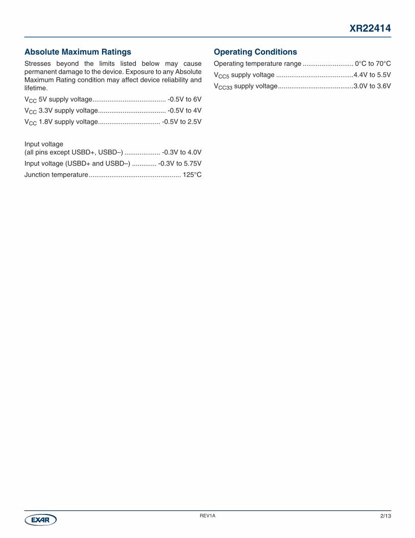
Top View, QFN48
Electrical Characteristics (Continued)Unless otherwise noted: TA = 0°C to 70°C; VCC5 = 4.4V to 5.25V or VCC33 = 3.0V to 3.6V.
Symbol Parameter Conditions Min Typ Max Units
Non-USB I/O Pins
VIL Input low voltage -0.3 0.8 V
VIH Input high voltage 2.0 5.5 V
VOL Output low voltage IOL = 4mA 0.4 V
VOH Output high voltage IOL = -4mA 2.4 V
IIL Input low leakage current ±10 μA
IIH Input high leakage current ±10 μA
CIN Input pin capacitance 5 pF
USB I/O Pins(1)
3.3V Regulated Power Output
3V3_OUT Output voltage Max load current 100mA 3.0 3.3 3.6 V
NOTE: 1. See USB 2.0 Specification for USB I/O pins DC Electrical Characteristics.
Pin Configuration
Top View, LQFP48
13 14 15 16 17 18 19 20 21 22 23 24
36
35
34
33
32
31
30
29
28
27
26
25
48 47 46 45 44 43 42 41 40 39 38 37
1
2
3
4
5
6
7
8
9
10
11
12
OVC2#
PWR2#
VCC18
PWR3#
OVC3#
GND
OVC4#
PWR4#
VCC18
GND
XTALOUT
XTALIN
BUS_PWR#
VBUS_SENSE
EXT_RST#
GND
VCC33
UP_DP
UP_DM
VCC18
REXT
VCC33
1V8_OUT
GND
OVC1
#
PWR1
#
LED4
LED3
LED2
LED1
LED_
CTL
VCC3
3
TEST
3V3_
OUT
VCC5
REG_
EN#
VCC3
3
DM4
DP4
GND
DM3
DP3
VCC3
3
DM2
DP2
GND
DM1
DP1
XR22414LQFP48
242322212019181716151413
373839404142434445464748
12
11
10
9
8
7
6
5
4
3
2
1
25
26
27
28
29
30
31
32
33
34
35
36OVC2#
PWR2#
VCC18
PWR3#
OVC3#
GND
OVC4#
PWR4#
VCC18
GND
XTALOUT
XTALIN
BUS_PWR#
VBUS_SENSE
EXT_RST#
GND
VCC33
UP_DP
UP_DM
VCC18
REXT
VCC33
1V8_OUT
GND
VCC5
REG_
EN#
OVC1
#
PWR1
#
LED4
LED3
LED2
LED1
LED_
CTL
VCC3
3
TEST
3V3_
OUT
VCC3
3
DM4
DP4
GND
DM3
DP3
VCC3
3
DM2
DP2
GND
DM1
DP1
CPAD
XR22414QFN48

XR22414
5/13REV1A
Pin Functions
Pin Number Pin Name Type Description
1 OVC2# IDownstream port 2 over current indicator, active low. If global over-current protection is selected by connecting PWR4# to ground, this pin is unused and should be tied to ground.
2 PWR2# OPower enable for port 2 downstream device. Asserted if OVC2# input is asserted in individual power mode or XR22414 is not configured. Unused when ganged power control mode is selected by connecting PWR4# to ground.
3 VCC18 PWR 1.8V power input
4 PWR3# OPower enable for port 3 downstream device. Asserted if OVC3# input is asserted in individual power mode or XR22414 is not configured. Unused when ganged power control mode is selected by connecting PWR4# to ground.
5 OVC3# IDownstream port 3 over current indicator, active low. If global over-current protection is selected by connecting PWR4# to ground, this pin is unused and should be tied to ground.
6 GND Ground
7 OVC4# IDownstream port 4 over current indicator, active low. If global over-current protection is selected by connecting PWR4# to ground, this pin is unused and should be tied to ground.
8 PWR4# I/OPower enable for port 4 downstream device. Asserted if OVC4# input is asserted in individual power mode or XR22414 is not configured. If connected to ground, enables Ganged Power Control Mode and Global Over-Current Protection mode.
9 VCC18 PWR 1.8V power input
10 GND PWR Ground
11 XTALOUT O 12MHz crystal feedback output
12 XTALIN I12MHz +/- 50 ppm crystal input with load capacitance rating of 16-20pF. An external 3.3V clock may be used instead on on XTALIN leaving XTALOUT unconnected.
13 VCC33 PWR 3.3V power input
14 DM4 I/O Downstream port 4 USB D- data
15 DP4 I/O Downstream port 4 USB D+ data
16 GND PWR Ground
17 DM3 I/O Downstream port 3 USB D- data
18 DP3 I/O Downstream port 3 USB D+ data
19 VCC33 PWR 3.3V power input
20 DM2 I/O Downstream port 2 USB D- data
21 DP2 I/O Downstream port 2 USB D+ data
22 GND PWR Ground
23 DM1 I/O Downstream port 1 USB D- data
24 DP1 I/O Downstream port 1 USB D+ data
25 GND PWR Ground
26 1V8_OUT PWR1.8V power output from internal 3.3V to 1.8V regulator, may be used to power VCC18 power inputs. Must be decoupled with minimum of 10uF
27 VCC33 PWR 3.3V power input
28 REXT I External bias resistor. Connect 2.7kOhm 1% resistor from this pin to GND
29 VCC18 PWR 1.8V power input
30 UP_DM I/O Upstream port USB D- data
31 UP_DP I/O Upstream port USB D+ data

XR22414
6/13REV1A
Pin Number Pin Name Type Description
32 VCC33 PWR 3.3V power input
33 GND PWR Ground
34 EXT_RST# I External reset input, active low. Must be asserted for a minimum of 10uS
35 VBUS_SENSE I Connect to VBUS from USB host. In self-powered mode, indicates presence of host VBUS power
36 BUS_PWR# IBus power indicator, active low. For bus powered mode, connect to ground. For self powered mode, connect to logic ‘1’.
37 REG_EN# IActive low enable of internal 5V to 3.3V regulator. Connect to logic ‘1’ when XR22414 is powered by 3.3V.
38 VCC5 PWR5V power to internal 5V to 3.3V regulator. When XR22414 is powered by 3.3V, VCC5 should not be connected to 5V, and REG_EN# should be tied to logic ‘1’.
39 3V3_OUT PWR3.3V power output from internal 5V to 3.3V regulator, may be used to power VCC33 power inputs if enabled by REG_EN# pin. Must be decoupled with minimum of 10 uF. Leave unconnected if XR22414 is powered by external 3.3V.
40 TEST I Test mode enable. Tie to ground for normal device operation
41 VCC33 PWR 3.3V power input
42 LED_CTL I/O LED hub active indicator. May also be used in conjunction with port status LEDs. Refer to Figure 4.
43 LED1 I/OPort 1 LED Indicator. Max source current 3mA. May be used in conjunction with DRV pin. Refer to Figure 4. Connecting LED1 to ground marks downstream port 1 as non-removable device.
44 LED2 I/OPort 2 LED Indicator. Max source current 3mA. May be used in conjunction with DRV pin. Refer to Figure 4. Connecting LED2 to ground marks downstream port 2 as non-removable device.
45 LED3 I/OPort 3 LED Indicator. Max source current 3mA. May be used in conjunction with DRV pin. Refer to Figure 4. Connecting LED3 to ground marks downstream port 3 as non-removable device.
46 LED4 I/OPort 4 LED Indicator. Max source current 3mA. May be used in conjunction with DRV pin. Refer to Figure 4. Connecting LED4 to ground marks downstream port 4 as non-removable device.
47 PWR1# OPower enable for port 1 downstream device in individual power mode. Asserted if OVC1# input is asserted in individual or global power mode or XR22414 is not configured. Used as global power control pin if ganged power control mode is selected by connecting PWR4# to ground..
48 OVC1# IDownstream port 1 over current indicator in individual current-sensing mode, active low. If PWR4# is tied to ground, this pin is a global over-current sense input.
49 CPad PWR Connect QFN package center pad to PCB ground plane with thermal vias.
NOTE: Type: I = Input, O = Output, I/O = Input/Output, PWR = Power, OD = Open-Drain.

XR22414
7/13REV1A
Functional Block Diagram
XR22414 USB Host
Downstream Phy #1
Device #1 Device #2 Device #3 Device #4
Downstream Phy #2
Downstream Phy #3
Downstream Phy #4
TT #1
Port Routing Switch
Downstream Port Controller
Upstream Phy
Upstream Port Controller
HubController
OvercurrentDetection
PowerControl
3.3V to 1.8VRegulator
Hub Activity
Indicator
LED Controller
Oscillator
PLL (x40)
PortIndicators
12MHz
480MHz
5V to 3.3VRegulator
TT #2 TT #3 TT #4
XR22414
8/13REV1A
Applications Information
Functional DescriptionThe XR22414 hub has a multiple transaction translator architecture that provides one transaction translator (TT) for each of the downstream USB ports. The transaction translators allow the USB 2.0 hub to take incoming high speed packets from the USB host on the upstream port and translate these commands, if necessary to full or low speed devices on any of the 4 downstream ports. The MTT architecture allows for higher bandwidth as the 4 individual ports are not constrained by a shared resource.
USB InterfaceThe hub function of the XR22414 supports one configuration and utilizes the following USB endpoints:
■■ Control endpoint
■■ Status change endpoint
The XR22414 hub may be configured for bus powered mode with a maximum power of 500mA or self-powered mode by connecting the BUS_PWR# pin to the appropriate logic state. In bus powered mode, downstream ports are limited to low power (100mA or less). When self-powered, downstream devices can draw up to 500mA on each of the four ports.
USB Vendor IDExar’s USB vendor ID is 0x04E2.
USB Product IDExar’s USB hub product ID is 0x0414.
Device ResetThe XR22414 has both an automatic power-up reset and an external hardware pin reset. Strapping option for ganged power enables and global over-current sensing are selected by tying the PWR4# pin to logic ‘0’. This pin is sampled at device reset and the resulting option selected is set.
USB SuspendAll USB peripheral devices must support the USB suspend mode in bus powered mode. Per USB standard, the XR22414 device will begin to enter the suspend state if it does not detect any activity, (including Start of Frame or SOF packets) on its USB data lines for 3ms. The peripheral device must then reduce power consumption from VBUS power within the next 7 ms to the allowed limit of 2.5mA for the suspended state. Note that in this context, the “device” is all circuitry (including the XR22414) that draws power from the host VBUS. Each attached downstream port is also allowed an additional 2.5mA of suspend current. If no devices are connected to the XR22414 downstream ports, the USB host will suspend the hub.
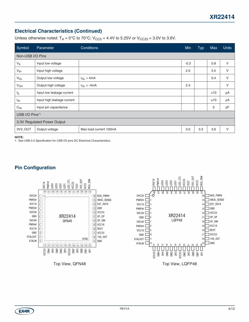
Individual vs. Ganged Power Control and Global Over-current protection modeGanged power control mode is enabled when PWR4# is tied to ground. In this mode only the PWR1# output pin is used for power control and the remaining PWR# pins are unused and should be left unconnected. Global over-current protection mode is also enabled when PWR4# is tied to ground. In this mode only OVC1# input pin is used for current sensing and the remaining OVC# pins should be connected to ground. Figure 1 depicts ganged power control / global over-current protection. Figure 2 depicts individual mode power and over-current modes for ports 1 and 2 (repeat for ports 3 and 4).
Figure 1: Ganged Power Control and Global Over-Current Protection Mode
OVC1#
OVC2#
OVC3#
OVC4#
PWR1#
PWR2#
PWR3#
PWR4#
XR22414
5V2A
To VBUSinput of all
downstreamdevices
Polymeric PTC

XR22414
9/13REV1A
USB Hub DriversAll Operating Systems provide a native USB hub device driver for the XR22414 device to operate. No other device drivers are necessary for the XR22414.
Regulated 3.3V Power OutputThe XR22414 internal voltage regulator provides 3.3VDC output power when the device is powered by 5V input. The 3.3V output can be utilized by other circuitry. Refer to Electrical Characteristics on page 3 for maximum power capability.
Downstream Port LED IndicatorsFour port indicator (LED1 - LED4) pins, provide status of connection of downstream devices. Ports with permanently connected devices should ground their respective port LED indicator. Ports using LED indicators may configure status LEDs in a number of configurations in conjunction with the DRV pin. Figure 3 and Figure 4 show alternate configurations for LED status indicators. Green / amber LEDs in Figure 4 are implemented per USB hub specification USB 2.0 spec, chapter 11.
Figure 2: Individual Power Control and Over-Current Protection Mode
Figure 3: Port status LED indicators disabled
ENA
FLGA
FLGB
ENB
RSETA
OUTA
IN
GND
OUTB
RSETB
XRP2528
OVC1#
OVC2#
OVC3#
OVC4#
PWR1#
PWR2#
PWR3#
PWR4#
XR22414
3.3V5V
To VBUS ofPort 1
To VBUS ofPort 2
Duplicate forPort 3 and 4
LED1
LED2
LED3
LED4
DRV
XR22414
Port 1 device isnon-removable
Port 2-4 devices areremovable but port LED
status is disabled
Port status LEDindicators disabled

XR22414
10/13REV1A
Figure 4: Port status LED indicators enabled dual LED mode
LED1
LED2
LED3
LED4
DRV
XR22414
Green
Amber470
Green
Amber470
Port 2 and 4 devices are removable
with Green/AmberLED indicatorsper USB hubspecification
470
Green
Hub active indicator (optional)
Port 1 enabled but does not use port status indicator
XR22414
11/13REV1A
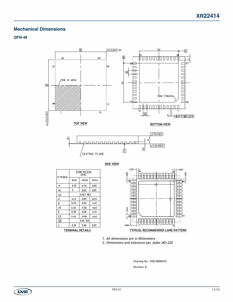
Mechanical Dimensions
QFN-48
Revision: B
Drawing No.: POD-00000101
TOP VIEW BOTTOM VIEW
TERMINAL DETAILS TYPICAL RECOMMENDED LAND PATTERN
SIDE VIEW
1. All dimensions are in Millimeters2. Dimensions and tolerance per Jedec MO-220

XR22414
12/13REV1A
Mechanical Dimensions
LQFP-48
- Control dimensions are in Millimeters- Jedec MS 026
Drawing No. : POD - 00000096
Revision: A
SIDE VIEW
TOP VIEW
TYPICAL RECOMMENDED LAND PATTERNTERMINAL DIMENSION
DETAIL A

www.exar.com
XR22414
Exar Corporation reserves the right to make changes to the products contained in this publication in order to improve design, performance or reliability. Exar Corporation conveys no license under any patent or other right and makes no representation that the circuits are free of patent infringement. While the information in this publication has been carefully checked, no responsibility, however, is assumed for inaccuracies.
Exar Corporation does not recommend the use of any of its products in life support applications where the failure or malfunction of the product can reasonably be expected to cause failure of the life support system or to significantly affect its safety or effectiveness. Products are not authorized for use in such applications unless Exar Corporation receives, in writing, assurances to its satisfaction that: (a) the risk of injury or damage has been minimized; (b) the user assumes all such risks; (c) potential liability of Exar Corporation is adequately protected under the circumstances.
Reproduction, in part or whole, without the prior written consent of Exar Corporation is prohibited. Exar, XR and the XR logo are registered trademarks of Exar Corporation. All other trademarks are the property of their respective owners.
©2016-2017 Exar Corporation
48720 Kato RoadFremont, CA 94538USA
Tel.: +1 (510) 668-7000Fax: +1 (510) 668-7001
Email: [email protected]
XR22414_DS_xxxx17 13/13REV1A
Ordering Information(1)
Part Number Operating Temperature Range Lead-Free Package Packaging Method
XR22414CL48TR-F 0°C to +70°CYes(2)
48-pin QFN Reel
XR22414CV48TR-F 0°C to +70°C 48-pin LQFP Reel
XR22414CL48EVB XR22414 48-pin QFN Evaluation Board
XR22414CV48EVB XR22414 48-pin LQFP Evaluation Board
NOTE: 1. Refer to www.exar.com/XR22414 for most up-to-date Ordering Information.2. Visit www.exar.com for additional information on Environmental Rating.
Revision History
Revision Date Description
1A February 2017 Initial Release