Embed Size (px)
Citation preview
PESIT BANGALORE SOUTH CAMPUS education for the real world
PESIT – BANGALORE SOUTH CAMPUS
QUESTION BANK
CHAPTER – 1: ANALOG ELECTRONICS
THEORY QUESTIONS
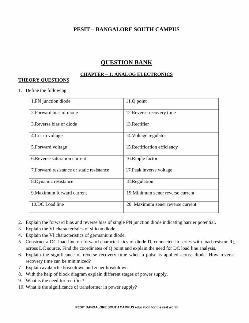
1. Define the following
1.PN junction diode
11.Q point
2.Forward bias of diode
12.Reverse recovery time
3.Reverse bias of diode
13.Rectifier
4.Cut in voltage
14.Voltage regulator
5.Forward voltage
15.Rectification efficiency
6.Reverse saturation current
16.Ripple factor
7.Forward resistance or static resistance
17.Peak inverse voltage
8.Dynamic resistance
18.Regulation
9.Maximum forward current
19.Minimum zener reverse current
10.DC Load line
20. Maximum zener reverse current.
2. Explain the forward bias and reverse bias of single PN junction diode indicating barrier potential.
3. Explain the VI characteristics of silicon diode.
4. Explain the VI characteristics of germanium diode.
5. Construct a DC load line on forward characteristics of diode D, connected in series with load resistor RL
across DC source. Find the coordinates of Q point and explain the need for DC load line analysis.
6. Explain the significance of reverse recovery time when a pulse is applied across diode. How reverse
recovery time can be minimized?
7. Explain avalanche breakdown and zener breakdown.
8. With the help of block diagram explain different stages of power supply.
9. What is the need for rectifier?
10. What is the significance of transformer in power supply?
11. Explain the operation of half wave rectifier with relevant circuit diagram and waveforms.
12. What are the disadvantages of half wave rectifier? How it is overcome?
13. Explain the operation of cetertap full wave rectifier with relevant circuit diagram and waveforms.
14. What are the disadvantages of center tap full wave rectifier? How it can be overcome?
15. Explain the operation of full wave bridge rectifier with relevant circuit and waveform.
16. Explain the operation of half wave rectifier with C filter using relevant circuit diagram waveforms and
formulas.
17. Explain the operation of center tap full wave rectifier with C filter using relevant circuit diagram
waveforms and formulas.
18. Explain the operation of bridge wave rectifier with C filter using relevant circuit diagram waveforms and
formulas.
19. Design voltage regulator using zener diode.
DERIVATIONS
1. Derive an expression for average load current and load voltage of half wave rectifier
2. Derive an expression for average load current and load voltage of center tap full wave rectifier
3. Derive an expression for average load current and load voltage of bridge wave rectifier
4. Derive an expression for RMS load current and RMS load voltage of half wave rectifier
5. Derive an expression for RMS load current and RMS load voltage of center tap full wave rectifier
6. Derive an expression for RMS load current and RMS load voltage of bridge wave rectifier
7. Evaluate ripple factor of a half wave rectifier.
8. Evaluate ripple factor of a center tap full wave rectifier
9. Evaluate ripple factor of a bridge wave rectifier.
10. Prove that peak inverse voltage of half wave rectifier is peak input voltage.
11. Prove that peak inverse voltage of center tap full eave rectifier is twice the peak input voltage.
12. Prove that peak inverse voltage of bridge wave rectifier is peak input voltage.
13. Prove that efficiency η=40% for half wave rectifier.
14. Prove that efficiency η=80.2% for center tap wave rectifier.
15. Prove that efficiency η=80.2% for bridge wave rectifier
PROBLEMS
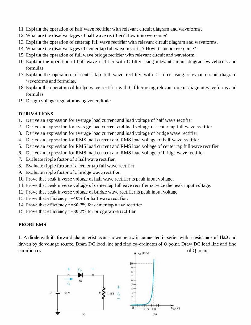
1. A diode with its forward characteristics as shown below is connected in series with a resistance of 1kΩ and
driven by dc voltage source. Dram DC load line and find co-ordinates of Q point. Draw DC load line and find
coordinates of Q point.

PESIT BANGALORE SOUTH CAMPUS education for the real world
2. Find the load resistance in the circuit shown using the diode forward characterstics provided
3. Find minimal fall time for voltage pulses applied to a diode with reverse recovery time of 4 ns.
4. Estimate the maximum reverse recovery time for a diode for an input pulse with 0.5μs fall time.
5. A FWR with capacitor is supplying resistive load of 1kΩ. If the filter capacitor is 500μF. Calculate
ripple factor.
6. In a FWR, the input is 30-0-30 v transformer. The load and diode forward resistance are 100Ω and
10Ω respectively. Calculate average voltage, rectification efficiency and percentage regulation
7. A FWR with capacitor is supplying resistive load fo 400Ω in parallel with a capacitor 500μF. If the
AC supply voltage is 230sin314t V. Calculate ripple factor and DC current.
8. Design a zener regulator with the fallowing specifications
Unregulated dc input voltage Vi: 8-12 volts
Load Current, IL=20mA
Regulated dc output voltage Vo: 5 Volts
Minimum Zener current Iz min: 5mA
Maximum Zener current Iz max: 80 mA
9. Design a zener regulator with the fallowing specifications
Unregulated dc input volyage Vi: 13-17 volts
6mA

Load Current, IL=10 mA
Dc output voltage Vo : 10 Volts
Minimum Zener current Iz min: 5 mA
Maximum power dissipation in zener, Pzmax: 500mW
10. A diode with Vf=0.7v is connected as a half wave rectifier. The load resistance is 600Ω and the (rms)
AC input is 24v. Determine the peak output voltage, the peak current and peak reverse voltage.
11. Design a zener regulator with the fallowing specifications
Unregulated dc input volyage Vi: 10 volts ± 20%
Load Current, IL=10mA
Regulated dc output voltage Vo : 5 Volts
Minimum Zener current Iz min: 5mA
Maximum Zener current Iz max: 80 mA
Multiple choice questions
1). A general purpose diode is more likely to suffer avalanche breakdown rather than Zener breakdown
because
a). its leakage current is small b). It has weak covalent bonds c) it is lightly doped d). it has low reverse
resistance
Ans C) It is lightly doped
2). The turn on voltage of a Ge diode is
a). 0.7 b). 0.3 c). 1.0 d). 0.1 Ans - 0.3
3). The PIV is the maximum reverse voltage that can be applied to a diode without
a) Burnout b) Destruction c) Overheating d). Charging
Ans b).Destruction
4). Leakage current of a junction diode --------
a). Decrease with temperature b). is due to majority carriers c). depends on the method of its fabrication
d). is in the range of mili- Amp or Micro Amp

PESIT BANGALORE SOUTH CAMPUS education for the real world
Ans - is in the range of mili - Amp or Micro Amp
5). In the Forward region of its characteristics, a diode appears as
a). an OFF switch b). a high resistance c). a Capacitor d). an ON Switch
Ans - An ON Switch
6). Under small signal operation of a diode
a). its bulk resistance increases b). its junction resistance predominates c). it acts like a closed switch d). it
behaves a clippe Ans – b).Its junction resistance predominates
7). The depletion region of a P-N junction is formed
a). During the manufacturing process b). When forward bias is applied to it c). Under reverse Bias d). When
its temperature is reduced
Ans – a). During the manufacturing process
8). The width of the depletion layer of a junction
a). Decreases with light Doping b). Increases with heavy Doping c). is independent of the applied voltage d).
is increased under Reverse bias
Ans – d).is increased under Reverse bias
9). Point out the WORNG statement. Barrier potential of a P-N Junction is a function of
a). Diode design b). Temperature c). Forward bias d) Doping density
Ans – c).Forward bias
10). The width of depletion region of an unbiased P-N junction is about a few
a). μm b). mm c). cm d). nm
Ans – c) cm
11). Zener breakdown occurs
a). mostly in Germanium junctions b). Due to rupture of covalent bonds c). in lightly doped junctions d) Due
to thermally-generated minority carriers
Ans – b) Due to rupture of covalent bonds
12). Avalanche break down is primarily dependent on the phenomenon of
a). Collision b).Doping c). ionization d). Recombination
Ans- a). Collision
13). Reverse current in a silicon junction nearly doubles for every …………Degree centigrade rise in
temperature a). 10 b). 2 c). 6 d). 5
Ans- a)10
14). The depletion region of a semiconductor diode is due to
a). absence of the current carriers b).Reverse Biasing c). Forward Biasing d). Crystal doping
Ans –a) Absence of the current carriers
15). The ripple factor of a power supply is a measure of a). Its filter efficiency b). Its voltage regulation c).
Diode rating d). Purity of the power output
Ans- d)Purity of the power output
16). A Diode has ----
a).One PN junction b). Two PN junction c). Three PN junction d). none of the above
Ans- a).One PN junction
17). The knee voltage of the Diode is approximately equal to ----
a).applied voltage b). breakdown voltage c). forward voltage d).barrier potential
Ans- d).barrier potential
18). The Diode current is large , during ---- bias
a).F.W. b).R.V. c). poor d) non of the above
Ans- a).F.W.
19). The Diode is a ---- device
a).non linear b).bilateral. c). linear d) non of the above
Ans- a).non linear
TRANSISTORS
1. Explain the word transistor. Clearly show the biasing arrangement of the PNP an NPN transistor for
conduction.
2. Give the concept of DC load line.
3. With a neat sketch, clearly show the various current components in a PNP transistor and hence establish
the relevant equations.
4. Sketch and explain the current components in transistor. Hence define emitter efficiency, transport factor
and large signal current gain.
5. What are the three regions of operation of a BJT? What are the biasing conditions for each of these
regions? Mention the region in which BJT acts as an amplifier.
PESIT BANGALORE SOUTH CAMPUS education for the real world
6. Clearly explain the effect of temperature and (Beta) on the operating point stability.
7. Discuss the causes of bias instability in transistor.
8. Sketch and explain the current components crossing each junction of a transistor biased in the active
region.
9. A transistor is capable of providing amplification. Explain the basic transistor amplifier with suitable
diagrams.
10. Bring out the relationship between (Alpha) (Beta) of transistor.
11. Draw the transistor circuit in CB configuration. Sketch the output characteristics. Indicate ‘active’,
‘saturation’ and ‘cutoff region’. Brief explain the nature of those curves.
12. For a transistor working in CB configuration, explain the input and output characteristics with a
suitable diagrams.
13. Sketch and explain the input and output characteristics of a transistor in CE configuration on the
output characteristics. Clearly indicate the 3 operating regions and mention the biasing requirement for
each.
14. Compare amongst CC, CB, CE configurations of a transistor amplifier in terms of the current gain, the
voltage gain, and the input impedance and output impedance.
15. Draw a fixed bias circuit and explain why the circuit is unsatisfactory if the transistor is replaced by
another of the same type. Derive an expression for its stability factor.
16. Draw the sketch of the output characteristics of a transistor in common emitter configuration? Indicate
various region operation and comment for the shape of characteristics qualitatively.
17. Discuss the causes of unstability in a transistor.
Multiple choice question
1). A Transistor has
a). One P-N Junction b). Two P-N Junction c). Three P-N Junction 4). Four P-N Junction
Ans- Two P-N Junction
2). The number of depletion layer in a Transistor is a). 1 b). 2 c). 3 d). 4
Ans – 2
3). The base of the Transistor is ……………. Doped
a). Heavily 2). Lightly 3). Moderately 4). None of the above
Ans- Lightly
3). The element that has biggest size in a transistor is
a). Collector b). Emitter c). Base d). Emitter- Base junction
Ans- Collector
4). In a PNP transistor, the current carriers are
a). Acceptor Ions b). Donar ions c). Free electrons d). Holes
Ans- Holes
5). The Collector of the Transistor is ……………. Doped
a). Heavily 2). Lightly 3). Moderately 4). None of the above
Ans- Moderately
6). The Emitter of the Transistor is ……………. Doped
a). Heavily 2). Lightly 3). Moderately 4). None of the above
Ans- Heavily
7). A transistor is a ………….. operated device.
a). Current b). Voltage c). Both Current and Voltage d). Non of the above
Ans - Current
8). In a NPN transistor…….are minority carriers
a). Free electrons b). Holes c). Acceptor Ions d). Donar ions
Ans – Holes
9). In a transistor, the base current is about …………. Of emitter current
a). 25% b). 20% c). 50% d). 5%
Ans – 5%
10). At the Base-emitter junction of a transistor is
a). Reverse Biased b). A wide depletion layer c). Low resistance d). Non of the above
Ans- Low resistance
11). The input impedance of the transistor is ………..
a) High b). Low c). Very high d). Almost Zero
Ans- Low
12). In a transistor…………….
a) IE = Ic- IB b). Ic = IE + IB c). IB= Ic + IE d) IE = Ic+ IB
Ans - IE = Ic+ IB
13). The value of Alpha of a transistor is …………
a). > 1 b). < 1 c). = 1 d). none of the above
Ans - < 1
13). The value of β of a transistor is …………
PESIT BANGALORE SOUTH CAMPUS education for the real world
a). > 1 b). < 1 c). = 1 d). Between 20 and 500
Ans - Between 20 and 500
14). The output impedance of a transistor is ……………
a). High b). Low c). zero d). Very Low
Ans - High
15). The relation between and β is
a). /1 b). 1/ 1 c). 1/ d). 1/ 1
Ans- /1
16). The most commonly used transistor Configuration is
a). CCC b). CEC c). CBC d). None of the above
Ans - CEC
17). The voltage gain of a transistor connected in CCC is
a). Equal to 1 b). More than 10 c). More than 100 d). Less than 1
Ans - Less than 1
18). In a transistor, signal is transferred from a ……………. Circuit
a). High resistance to Low resistance b). Low resistance to High resistance
c). Low resistance to Low resistance d).High resistance to High resistance.
Ans - Low resistance to High resistance
19). The Arrow in the symbol of a transistor indicates the direction of ……………
a). Electron current in the emitter b). Electron current in the Collector c). Hole current in the emitter d). None
of the above
Ans - Electron current in the emitter
20). The leakage current in CE configuration is ……. That in CB arrangement
a). More than b). Less than c). The same as d). None of the above
Ans - More than
21). The most commonly used SC material for the manufacture of a transistor is
a). Ge b). Si c). Cu d). None of the above
Ans - Si
22). The collector – Base junction in a transistor has
a). F.W.B at all times b). R.V.B at all times c). Low resistance d). None of the above
Ans - R.V.B at all times
BIASING METHODS
1. Explain the concept of Load line in case of transistors and thus discuss the biasing techniques applied to
NPN transistors.
2. What do you mean by stabilization?
3. Define stability factor? Find the relationship between stability factor and Ib? What is its ideal value?
4. Give the essential requirements of stabilization.
5. Derive the stability factor for the feedback resistor circuit.
6. Find the stability factor ‘S’ for self-biasing circuit?
7. Find the stability factor ‘S’ for Voltage divider bias circuit
8. Find the stability factor ‘S’ for fixed bias circuit.
9. Define Operating point. Explain why Operating point should be stable.
10. Determine the operating point for the fixed bias circuit for the following given parameters VCC=12 volts,
RB=240K, RC=2.2K, Beta=50
11. Determine the operating point for the feedback resistor circuit for the following given parameters VCC=12
volts, RB=240K, RC=2.2K, Beta=100,RE=2.2K
12. Determine the operating point for the voltage divider bias circuit for the following given parameters
VCC=12 volts, RE=1.2K, RC=5.6K, Beta=50,R1=82K, R2=22K
13. Design a voltage divider bias circuit if operating point + 10V,2mA and VCC=18V, neglect VBE
14. For the CE circuit RB between base and supply Vcc is 1.5 Mohm, RC between
collector and Vcc is 5 Kohm, Vcc=30volts. Draw the DC load line and mark the dc
operating point on it. Assume =100 and neglect VBE.
Multiple choice questions
1).Transistor biasing represents ………….. Conditions.
a). AC b). DC c). Both AC and DC d). None of the above
Ans - DC
2). Transistor biasing is done to keep ………… in the circuit
a). Proper direct current b). Proper AC
c). The base current Small d). Collector current Small.
Ans - Proper direct current.
PESIT BANGALORE SOUTH CAMPUS education for the real world
3). Operating point represents ……………..
a). Values of IC and VCE when signal is applied b). The magnitude of the signal
c). Zero signal values of IC and VCE d). None of the above
Ans- Zero signal values of IC and VCE
4). Improper biasing of a Transistor circuit leads to
a). excessive heat production at collector terminal b). distortion in output signal
c). Faulty location load line d). Heavy loading emitter terminal
Ans- Distortion in output signal
5). The universal bias stabilization circuit is most popular because
a) Ic does not depend on the transistor characteristics b). Its Beeta instability is high
c). Voltage divider is heavily loaded by transistor base d) Ic = Ie
Ans - Ic does not depend on the transistor characteristics
6). Transistor Biasing is generally provided by a …………….
a). Biasing circuit b). Bias battery c). diode d). None of the above
Ans - Biasing circuit
7). For proper operation of the transistor , its collector should have
a). FWB b). RVB c). Very Small size d). None of the above
Ans - Proper RVB
8). The circuit that provides the best stabilization of operating point is …….
a). Base Resistor bias b). Collector feedback bias
c). Voltage Divider or Potential Divider Bias d). None of the above .
Ans - c). Voltage Divider or Potential
9). The point of intersection of the DC and AC load line represents……………
a). Operating point b). Current gain c). Voltage Gain d). None of the above .
Ans- a). Operating point
10). An ideal value of stability factor is ……………….
a). 100 b). 200 c). More than 200 d). 1
Ans - 1
11). The disadvantage of Base resistor method of transistor biasing is that it…….
a). is complicated b). is sensitive to changes in β

c) Provides high stability d). None of the above.
Ans - is sensitive to changes in β
12). The operating point is also called the …………….
a). Cut off point b). Quiescent point c). The maximum current point d). None of the above.
Ans - b). Quiescent point
13). For proper amplification by a transistor circuit, the operating point should be located at ………. Of the
DC load line.
a). The end point b). Middle point
c). The maximum current point d). None of the above.
Ans - b). Middle point
14). The disadvantage of Voltage Divider Bias is that it has ……
a). High stability factor b). Low base Current c). Many resistors d). None of the above.
Ans - c). Many resistors
15). Thermal runway occurs when …………….
a). Collector is RVB b). Transistor is not biased
c). Emitter is FWB d). Junction Capacitance is high.
Ans - b). Transistor is not biased
16). The purpose of resistance in the emitter circuit of a transistor amplifier is to ……
a). Limit the maximum IE b). Provide base- emitter bias
c). Limit the change in the IE d). None of the above.
Ans - c). Limit the change in the IE
17). In a transistor amplifier circuit , VCE = VCB + …….
a). VBE b). 2VBE c). 1.5 VBE d). None of the above.
Ans - VBE
18). The base resistor circuit is generally used in
a). Amplifier circuit b). Switching circuit
c). Rectifier circuit d). None of the above.
Ans- b). Switching circuit
19). The value of S factor of a collector feedback bias circuit is ………… that of base resistor bias.
a). The same as b). More than c). Less than d). None of the above
Ans - c). Less than

PESIT BANGALORE SOUTH CAMPUS education for the real world
20). The value of S factor of Base resistor bias is .
a). ( 1)B
R b). ( 1) c). ( 1) d). None of the above
Ans - ( 1)
21). In the design of a biasing circuit, the value of collector load RC is determined by
a)VCE consideration b). IB consideration c). VCE consideration d). None of the above
Ans- a). VCE consideration
22). If the value of the IC increases the value of the VCE…….
a). remains same b). Decreases c). Increases d). None of the above
Ans - b). Decreases
23). If the value of the Temperature increases the value of the VBE…….
a). remains same b). Decreases c). Increases d). None of the above
Ans - b). Decreases
24). The stabilization of operating point in potential divider method is provided by ….
a). RE Consideration b). RC Consideration c). VCC Consideration d). None of the above
Ans- a). RE Consideration
25). When the temperature changes , the operating point is shifted due to ……..
a). Changes in ICBO b). Changes in Vcc
c). Change in the value of circuit resistances d). None of the above
Ans - a). Changes in ICBO
26). An SCR has ……. PN Junction.
a). 2 b). 3 c). 4 d). None of the above
Ans- b). 3
CHAPTER – 2 : OPERATIONAL AMPLIFIERS
1. Discuss Integrated circuit. Briefly give the classification of digital IC’s based on the component
fabrication.
2. Draw the block schematic of an op-Amp and Explain the function of each stage.
3. What are the applications of op-amp.
4. What are the ideal characteristics of op amp.
5. Define and mention the importance of the following terms w.r.t. an op-amp
i) CMRR ii) Slew rate iii) PSSR iv) I/p offset voltage iv) Virtual ground.
6. Define for an op-amp i) CMRR ii) output offset voltage. What are their typical values for a 741 op-amp?
7. Explain the working of op-amp as i) Adder ii) Subtractor iii) Integrator.
8. Derive an expression for output voltage of an op-Amp.
i) Inverting amplifier
ii) ii) Adder
iii) iii) Integrator
iv) iv) Differentiator
9. Derive the expressions for voltage gain with feedback of
i) Inverting op-amp
ii) Non-Inverting op-amp
10. Explain how an op-amp can be configured as an adder and an integrator. Obtain the
output expression for both.
11. Mention a least of five parameters expected for an operational amplifier. What their
ideal expected values? What are their practical values for a 741 op-amp.
12. Explain op-amp as i) Voltage follower ii) Comparator.
13. Design an-adder circuit using an op-amp to obtain an output expression
Vo= 2 (0.1 V1 + V2 + 20V3) Where V1, V2 and V3 are inputs.
14. Calculate the output voltage of a three input summing amplifier given:
R1= 200 Kohm, R2=250 Kohm, R3=500Kohm, Rf=1Mohm, V1= -2V, V2=+2V,
V3=+1V.
Multiple choice questions
1). An OP-AMP is a -------- IC
a). Linear b). Low-rin c). Positive Feedback d). RC-Coupled
Ans- a). Linear
2). The open loop gain of an ideal OP-AMP is -------
a). Zero b). 100 c). ∞ d). Non of the above
Ans- c). ∞
3). An ideal OP-AMP is has -------

PESIT BANGALORE SOUTH CAMPUS education for the real world
a). Infinite Av b). Infinite Rv c). Zero Ro d). All the above
Ans- d). All the above
4). An ideal OP-AMP is has input resistance of ------- and output resistance of ----
a). Infinity ,Zero b). Infinity ,100 c).1KΩ, Zero Ro d). All the above
Ans- a). Infinity ,Zero
5). A Differential Amplifier ----
a). is a part of an Op-amp b). has one input and one output
c).has two outputs d). Answers (a) and (c)
Ans- d). Answers (a) and (c)
6). In Differential- mode ----
a).Opposite polarity signals are applied to the inputs b). The gain is one
c).The outputs are of different amplitudes d).Only one supply voltage is used
Ans- a).Opposite polarity signals are applied to the inputs
7). In the common mode ----
a). Both inputs are grounded b). Both outputs are connected together
c).An identical signals appears on both inputs d). The output signals are in phase
Ans- c).An identical signals appears on both inputs
8). The Common mode gain is ----
a). Very high b). Very low c).Always Unity d).Unpredictable
Ans- b). Very low
9). The Differential gain is ----
a). Very high b). Very low c).Dependent on input voltage d).About 100
Ans- a). Very High
9). The Differential gain is ----
a). Very high b). Very low c).Dependent on input voltage d).About 100
Ans- a). Very High
10). The Output of the Inverting OP-amp is ----
a). is in phase b). inverted c).100 degree phase shift d).Non of the above
Ans- b). inverted
11). The Output of the Non- Inverting OP-amp is ----
a). is in phase b). 100 degree phase shift c). 80 degree phase shift d).Non of the above
Ans- a). is in phase
12). A voltage follower ----
a). Has a voltage gain of 1 b). in non-inverting
c). Has no feedback resistor d).has all of these
Ans- d).has all of these
12). The Op-amp can amplify
a). a.c. signals only b). d.c. signals only
c). Both a.c. signals and d.c. signals d). Neither a.c. signals and d.c. signals
Ans- c). Both a.c. signals and d.c. signals
13). With Zero volts on both inputs, an OP-amp ideally should have an output ----
a). Equal to the positive supply Voltage b). Equal to the Negative supply Voltage
c). Equal to the zero Voltage d). Equal to the CMRR
Ans- c). Equal to the zero Voltage
14). For an OP-amp with negative feedback, the output is -------
a). Equal to the input b). increased
c). Fed back to inverting input d). Fed back to Non- inverting input
Ans- c). Fed back to inverting input
15). The input offset current equals the -------
a).Difference between two base currents b). Average of two base currents
c).Collector current divided by current gain d). None of these
Ans- a).Difference between two base currents
16). The input offset current equals the -------
a).Difference between two base currents b). Average of two base currents
c).Collector current divided by current gain d). None of these
Ans- a).Difference between two base currents
17). An Adder circuit provides an output voltage which is the ------ Sum of two or more input voltages
a).Algebraic b).Logical c).Both (a) and (b) d). None of these
Ans- a). Algebraic
18). An integrator converts a DC level into a linearly increasing ----- output.
a).Square b).Rectangle c).Triangle d). Ramp
Ans- d). Ramp
19). A Differentiator converts a linear ramp into a ----- dc output.
a).Variable b). Linear c).Constant d).Triangle
Ans- c).Constant

PESIT BANGALORE SOUTH CAMPUS education for the real world
20). A Differentiator is obtained by ------ the resistor and Capacitor of an integrator circuit
a).Interchanging b).Keeping the same c).Sputtering d).None of these
Ans- a).Interchanging
21). When in a negative feedback, bothR1 and Rf are reduced to zero, the circuit functions as
a).Integrator b).Subtractor c).Comparator d).Unity follower
Ans- d).Unity follower
CHAPTER –3: DIGITAL ELECTRONICS
1. Explain the conversions with one Example.
i)Decimal to Binary ii) Binary to decimal
iii) Decimal to octal iv) Octal to decimal
v) Decimal to Hexadecimal vi) Hexadecimal to decimal
2. Convert i) (284.65)10= (?)8=(?)16 ii) (ABFE)16=(?)2=(?)10
3. Perform the following
i) (57.6)8=(?)2= (?)16
ii) (193)16=(?)8 = (?)10
4. Use 1’s and 2’s compliment to perform
i) 1111 – 1101
ii) 10111 – 10011
iii) 1101 – 1001
5. To subtract 101 from 111 use 2’s and 1’s compliment.
6. Add (47)8 and (FA)16
7. Subtract F2A from 3BC and Vice versa .Use 2’s Compliment method.
Multiple choice questions
1).The digital systems usually operate on --------- number system
a).Binary b). decimal c). octal d).hexadecimal
Ans- a). Binary
2).The digital systems usually operate on --------- number system
a).Binary b). decimal c). octal d).hexadecimal
Ans- a). Binary

3).The base or radix of binary number system is
a).2 b). 10 c). 8 d).16
Ans- a).2
4).The base or radix octal number system is
a).2 b). 10 c). 8 d).16
Ans- c). 8
5).The base or radix decimal number system is
a).2 b). 10 c). 8 d).16
Ans- b). 10
6).The base or radix hexa decimal number system is
a).2 b). 10 c). 8 d).16
Ans- d).16
7).The binary system uses power of ---------- for positional value
a).2 b). 10 c). 8 d).16
Ans- a).2
8).The Hexa decimal system uses power of ---------- for positional value
a).2 b). 10 c). 8 d).16
Ans- d).16
9).The decimal number system uses power of ---------- for positional value
a).2 b). 10 c). 8 d).16
Ans- b). 10
10).The number (1000) 2 is equivalent to decimal number --------
a).10 b). 8 c). 4 d).16
Ans- b). 8
11).The binary addition 1+1+1 gives --------
a).101 b).10 c). 110 d).11
Ans- b). 10
12).Which of the following is NOT an octal number
a).19 b).77 c). 15 d).101
Ans-a). 19
13).Which of the following is NOT an octal number
PESIT BANGALORE SOUTH CAMPUS education for the real world
a).19 b).77 c). 15 d).101
Ans-a). 19
14).How many digits are there in octal number system?
a).7 b).8 c). 10 d).16
Ans-b). 8
15).How many digits are there in Decimal number system?
a).7 b).8 c). 10 d).16
Ans-c). 10
16).How many digits are there in Hexa decimal number system?
a).7 b).8 c). 10 d).16
Ans-d). 16
17).What is the equivalent binary number of (11.8125 )10
a).1011.1101 b).1010.1101 c). 1011.1000110101 d).1101.10001
Ans- a).1011.1101
18).What is the Decimal equivalent of (567 )8
a). 567 10 b). 887 10 c). 375 10 d). 501 10
Ans- c). 375 10
19).Is the sum 0f (B2CE5)16 and (AB2C3)16 is (15DFA8)16
a). YES b). NO
Ans- a). YES
20).The hexadecimal equivalent of binary number 1010 is
a). A 16 b). B 16 c). C 16 d). D 16
Ans- a). A 16
21).The number (1000101)2 is equivalent to octal
a). 54 b). 45 c).37 d). 25
Ans- b). 45
22).A binary digit is called
a). Byte b). nibble c). Bit d). non of the above
Ans- c). Bit
23).The ones complement of 1011111010 is
a). 1010101010 b).0000111101 c). 1110001110 d). 0100000101
Ans- d). 0100000101
24).In 2’s complement notation the sign bit is
a). LSB b).MSB c). LSD d). MSD
Ans- b).MSB
25).The 2’s complement of 1101 is
a). 1010 b).0101 c). 0011 d). 1100 Ans- c). 0011
26).BCD numbers are lies between
a). 0 to 9 b).0 to 15 c). 0 to 8 d). non of the above
Ans- a). 0 to 9
DIGITAL LOGIC
1. State and prove De-Morgan’s theorem for two variables.
2. Write the symbol, truth table and output expression for i) OR gate
ii) NAND gate iii) EX-OR gate iv) NOR gate v) AND gate vi) NOT gate.
3. Draw and Explain the circuit of current mode logic that works as an OR gate.
4. Realize an OR logic gate using diodes.
5. Explain the operation of NOT gate using a transistor.
6. Realize Ex-OR gate using NOT, OR and AND gates only.
7. Realize an AND logic gate using diodes.
8.Draw the logic circuit of full adder. Write Truth table and expression for a
3 input full adder.
9.Write the truth table of a full adder and explain how it can be constructed
using half adders.
10. Draw the circuit of full adder and write its truth table.
11. Show the logic diagram of a clocked RS flip flop with truth table.
12. Show the logic diagram of a clocked D flip flop with truth table.
13. Show the logic diagram of a clocked JK flip flop with truth table.
14. Show the logic diagram of a master slave flip flop with truth table.
15. Draw the architecture of 8086 and explain the each.
Multiple choice questions
1). A logic gate is an electronic circuit which

PESIT BANGALORE SOUTH CAMPUS education for the real world
a). makes a logic decisions b). allows electron flow only in one direction
c). works on binary algebra d). alternate between 0 and 1 values.
Ans - a). makes a logic decisions
2). In positive logic, logic state 1 corresponds to a). Positive voltage b). higher voltage level c). zero
voltage level d). lower voltage level.
Ans - b). higher voltage level
3). In negative logic, logic state 1 corresponds to
a).Negative voltage b). more Negative voltage c). zero voltage level d). lower voltage level.
Ans - d). lower voltage level.
4). The output of a 2-input OR gate is zero only when its
a).both inputs are zero b). either input is one
c). both inputs are one d). either input is zero
Ans - a).both inputs are zero
5). The output of a 2-input OR gate is zero only when its
a).both inputs are zero b). either input is one
c). both inputs are one d). either input is zero
Ans - a).both inputs are zero
6). The output of a 2-input AND gate is 1 only when its
a).both inputs are zero b). either input is one
c). both inputs are one d). either input is zero
Ans - c). both inputs are one
7). The output of a 2-input XOR gate is 1 only when its
a).both inputs are zero b). If only one input is 1 and other is zero
c). both inputs are one d). Non of the above
Ans - b). If only one input is 1 and other is zero
8). The output of a 2-input NAND gate is 0 only when its
a).both inputs are zero b). if one input is one

c). both inputs are one d). if one input is zero
Ans - c). both inputs are one
9). An XOR logic gate will have output as 1
a).When all inputs are 1 b). When odd number of inputs are 1
c). When even number of inputs are 1 d). When even number of inputs are 0
Ans - b). When odd number of inputs are 1
10). An AND gate
a).implements logic addition b). is equivalent to a series switching circuit
c). is equivalent to a parallel switching circuit d). non of the above
Ans - b). is equivalent to a series switching circuit
11). When an input electrical signal A= 10100 is applied to a NOT gate, its output signal is
a).01011 b).10101 c). 10100 d). 00101
Ans - a).01011
12). The only function of NOT gate is to a).stop
a signal b).recomplement a signal
c). invert an input signal d). Acts a universal gate
Ans - c). invert an input signal
13). In certain 2-input logic gate, when A=0,B=0, then output Y=1 and when A=0,B=1, then again output
Y=1. It must be ------- gate
a).XOR b).AND c). NOR d). NAND
Ans - d). NAND
14). The universal gate is a).XOR b).AND c). NOT d). NAND
Ans - d). NAND
15). The inputs of a NAND gates are connected together. The resulting circuit is -----
a). OR gate b).AND gate c). NOT gate d). Non of the above
Ans - c). NOT gate
16). The NAND gates is AND gate followed by -----
a). NOT gate b). AND gate c). OR gate d). Non of the above
Ans - a). NOT gate
17). Digital circuit can be made by the repeated use of -----
a). NAND gates b). AND gates c). OR gates d). NOT gates
Ans - a). NAND gates
18). The Derived gates are -----
a). EX-OR gate b). EX-NOR gate c). both (a) and (b) d). NAND Gate
Ans - c). both (a) and (b)
PESIT BANGALORE SOUTH CAMPUS education for the real world
19). In Boolean algebra, the bar sign(-) indicates -----
a). EX-OR operation b). AND operation c). NAND operation d).NOT operation
Ans - d). NOT operation
20). The given Boolean expression is Y AB AB if A=1 abd B=1 then Y=--
a). 1 b). 0 c). either 1 or 0 d). Non of the above
Ans - b). 0
CHAPTER –4 : COMMUNICATION SYSTEMS
1. Explain the need for modulation in Communication systems.
2. With a block diagram, explain the important feature of a communication system.
3. Draw the block diagram of Super hetrodyne receiver and explain the function of each
stage with necessary waveform.
4. Define i) Modulation
ii) Amplitude modulation
iii) Frequency modulation
iv) Phase modulation
v) Modulation index
5. Define AM and derive the necessary expression for AM.
6. What is amplitude modulation? Derive the Expressions for (a) Modulation index,
(b) Transmitted power in terms of carrier power and modulation index.
7. Explain with the waveforms the principal of amplitude modulation. Write the expression for AM wave.
8. For an AM wave, derive the expressions for modulation index and total power
contained in AM wave.
9. Obtain an expression for the total output power of the amplitude double side
band signal.
10.Explain the principle of frequency modulation. Draw the frequency spectrum
of FM wave.
11. What are the advantages of FM system over AM system? Make a critical
comparison.
12. Bring out the merits and demerits of AM and FM.

13.A carrier of 1 MHz with 400 watts of its power is amplitude modulated with a
sinusoidal signal of 2500 Hz. The depth of modulation is 75%. Calculate the
sideband frequencies, the band width, the power in the side bands and the total
power in the modulated wave.
14. The total power content of an AM wave is 2.64 Kwatts at a Modulation factor
of 80%. Determine the power content of i) Carrier ii) each side band.
15. A 500 watts 1 MHz carrier is amplitude modulated with a sinusoidal signal of
1kHz. The depth of modulation is 60%. Calculate the band width, power in the
side bands and the total power transmitted.
16. A carrier signal has a peak amplitude of 1000 volts. Modulation index is 40%.
Power is developed across a load of 100 Ohm. Determine the value of
transmitted power.
17. A 100 Mhz carrier wave is frequency modulated by a 10Khz sinusoidal
modulating signals. If the maximum frequency deviation is 50KHz. find the
modulation index.
18. Explain the principles of mobile communication.
19.List the applications and advantages of optical fiber communication.
Multiple choice questions
1). Modulation is done in ---------------
a).Transmitter b).radio receiver
c).Between Transmitter and radio receiver d).none of the above
Ans- a).Transmitter
2). In transmitter ---------- oscillator is used
a).Hartley b).RC phase shift c).wein bridge d).Crystal
Ans- d).Crystal
3). In An AM wave, useful power is carried by ---------
a).Carrier b).Sideband c).both Sideband and Carrier d). non of the above
Ans- b).Sideband
4). In An AM wave, B.W is --------- the audio signal frequency
a).Twice b).thrice c).four times d). non of the above
Ans- a).Twice
PESIT BANGALORE SOUTH CAMPUS education for the real world
5). In An AM wave, The --------- of the carrier is varied according to the strength of the signal
a).amplitude b).frequency c).phase d). non of the above
Ans- a).amplitude
6). In An AM wave, The majority of the power is in --------
a).lower side band b). upper side band c).carrier d). non of the above
Ans- c).carrier
7).If modulation is 100%, then signal amplitude is -------- carrier amplitude a).equal
to b). greater than c).lesser than d). non of the above
Ans- a).equal to
8).as modulation level is increased, the carrier power is ----- a).is increased b). remains the same c).is
decreased d). non of the above Ans- b). remains the
same
9). In An FM wave, The --------- of the carrier is varied according to the strength of the signal
a).amplitude b).frequency c).phase d). non of the above
Ans- b).frequency
10). In phase modulation, The --------- of the carrier is varied according to the strength of the signal
a).amplitude b).frequency c).phase d). non of the above
Ans- c).phase
11).De-modulation is done ----------------
a).receiving antenna b).transmitter c).radio receiver d). non of the above
Ans- c).radio receiver
12).If level of the modulation is increased ------------ power is decreased
a).carrier b).side bands c). carrier as well as side bands d). non of the above
Ans- b).side bands
13).In a radio receiver, noise is generally developed at -----------
a).IF stage b). RF stage c).receiving antenna d). audio stage
Ans- b). RF stage
14).Super heterodyne principle refers to -----------
a).using large number of amplifier stages b). using push pull circuit
c).obtaining lower fixed IF d). non of the above
Ans- c).obtaining lower fixed IF
15). Most of the amplification in a Superheterodyne receiver occurs at -----------
a).IF b). RF amplifier c).Audio amplifier d). detector
Ans- a).IF
16). in a Superheterodyne receiver, the input at the receiver stage is -
a).IF and RF b). AF and RF c). AF and IF d). RF and local oscillator
Ans- c). AF and IF
17). The major advantage of FM over AM is
a).Reception is less noisy b). higher carrier frequency c). smaller B.W d).none of the above
Ans- a).Reception is less noisy
18). Modulation refers to a low frequency signal controlling the ----------
a).Amplitude of the carrier b). frequency of carrier
c). phase of carrier d).may be any of these
Ans- d).may be any of these
19).In TV transmission, sound signal is ------------ modulated
a).Amplitude b). frequency c). phase d).non of the above
Ans- b). frequency
20).In FM, amplitude of the modulating signal determines
a).rate of frequency variation b). amplitude of frequency shift
c). tonal balance of transmission d).non of the above
Ans- b). amplitude of frequency shift
CHAPTER –5 : TRANSDUCERS
1. Define a transducer and list its advantages.
2. Explain electrical transducers and different types of electrical transducers.
3. What is the difference between a passive transducer and a active transducer.
4. Explain with diagram the functions of a resistive transducer
5. Describe with the help of a diagram the construction of a LVDT.
6. Explain thermistor.
7. Describe with a diagram the operation of a piezo-electric transducer.
Multiple choice questions
1).Piezo-electric transducers are --------- transducers
a).active b).passive c).mechanical d).none of the above
Ans- a). active
2). Thermistors are transducers in which ------- changes with change in temperature
a).voltage b). current c).ressistance d).none of the above
Ans- c). ressistance

PESIT BANGALORE SOUTH CAMPUS education for the real world
3).LVDT is ---------
a).light variable differential transducer b).linear variable differential transducer c).less variable differential
transducer d).none of the above Ans- b). linear variable differential transducer