Embed Size (px)
Citation preview

Quantum Encryption System - Synchronization
presentationpresentation MidtermMidterm
Project name: Synchronization for Quantum Encryption System
Project supervisor : Yossi Hipsh .Project performed by : Omer Mor Oded Belfer.
Quantum Encryption System - Synchronization
Project GoalProject Goal
The Synchronization system is an integral part of a quantum encryption system. The system will allow transferring messages in a safe way that a third unauthorized person would not be able to decipher .
The Synchronization system is needed to control the detector so it would be able to identify a single photon in an optic cable at a given time .
Quantum Encryption System - Synchronization
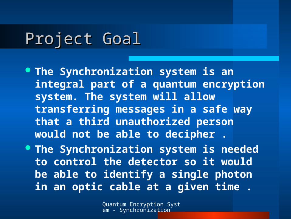
System requirementsSystem requirements
Locate and place a single photon with 1nSec accuracy resolution, in a 3nSec window.
The system should be a “stand alone” system and not depended on other components of the encryption system. For that we will need to simulate the other systems.
The system should be capable to work with very fast pulses.
The system will receive an Optic Sync signal and transfer it to a delayed electric signal, according to the photon arrival.

Quantum Encryption System - Synchronization
General Block schemeGeneral Block scheme
Syncronization System
Transmitter
PC
Receiver Optic Sync
Our part
Feedback
Electric 3nSec Sync pulse
Optic Data (Photon)
End Start

Quantum Encryption System - Synchronization
Synchronization system – Synchronization system – General Block schemeGeneral Block scheme
5V Surface
3.3V Surface
OrCad - Sync

Quantum Encryption System - Synchronization
General Block scheme –General Block scheme –5V Surface5V Surface
Optic Detector Board
Pulse stretcher
Splitter TTL
D.D.L TTL
D.D.L TTL
Ref – Test point
Computer
D.D.L TTL
*components marked in
yellow are detailed latter.
FPGA
Splitter TTL
Ref – T.P
To 3.3V
SyncPhoton
24nSec ≤ τ ≤ 0.5μSecPulse width 15-35nSecOptic syncFrom transmitter
5V Surface
Synchronization board.

Quantum Encryption System - Synchronization
General Block scheme –General Block scheme –3.3V Surface3.3V Surface
Mono Stable TTL To ECL
Splitter ECL
D.D.L ECL
D.D.L ECL
*components marked in
yellow are detailed latter.
Balanced to Unbalanced
Splitter ECL
Ref – Test point
To Receiver
30pSec ≤ τ ≤ 10nSec
Pulse width 3nSecFrom 5V TTL splitter
3.3V Surface
Synchronization board.
Splitter ECL
Balanced to Unbalanced
Ref – Test point
Quantum Encryption System - Synchronization
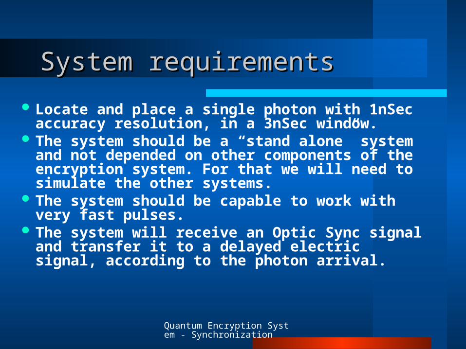
Special components –Special components –FPGA Input OutputFPGA Input Output
FPGA
Sync END
Computer
Sync START
D.D.L TTL
D.D.L TTL
D.D.L ECL
D.D.L ECL
D.D.L TTL
“Photon” – from splitter #1 “Sync” – from splitter #2
ADD1 Enable ADD2 Enable STR1
Valid photon 1STR2
Valid photon 2
’ *Valid photon’ will be used only if STR is not available.

Quantum Encryption System - Synchronization
Special components –Special components –Optic Detector BoardOptic Detector Board
Regulator9V Input Optic
Detector Transformator
Optic Sync. Input From transmitter
Pulse stretcher
Balanced Unbalanced
3.3V
Orcad Optic Detector

Quantum Encryption System - Synchronization
Special components –Special components –Mono StableMono Stable
Splitter ECL 1:2
D.D.L ECL
From TTL To ECL
D.D.L ECL
Flip Flop
CLK
_Q
QS
D
R
'1'
'0'
Quantum Encryption System - Synchronization
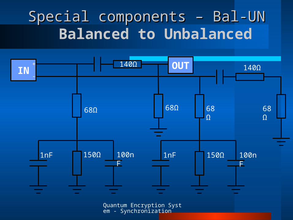
Special components – Bal-UNSpecial components – Bal-UN Balanced to Unbalanced
OUT
68Ω 68Ω 68Ω68Ω
140Ω 140Ω
150Ω 150Ω1nF 1nF100nF 100nF
IN+
-
Quantum Encryption System - Synchronization
Optic Detector BoardOptic Detector Board
The optic detector board will receive optic signal and translate it to a balanced electric pulse.
The board will supply the working needs for the Optic detector.
Input : optic signal (Laser).Output : Balanced electric pulse.
Quantum Encryption System - Synchronization
Aspects in choosing componentsAspects in choosing components Technological compatibility - (TTL/ECL, input and
output voltage) – most of the components we chose works in TTL technology because we needed width pulse for the computer and to the long delay device.
System compatibility - (with the transmitter, receiver and computer) – the transmitter output is an optic pulse so we needed to add an optic detector. The receiver input is in ECL technology so we need to convert the output technology to ECL.
Short Trise and Tfall – because we deal with a short an accurate pulses.
Available for purchase.øùéîú øëéáéí
Quantum Encryption System - Synchronization
System InputsSystem Inputs
Optic Sync pulse from the transmitter – we will simulate this pulse with a laser to test our system before integration with the transmitter.
STR1 & STR2 pulses from the receiver – feedback to check the photon arrival. We will simulate this pulse with the FPGA to test our system before integration with the receiver.
SYNC_START from the PC – starting the calibration sequence. We will assign switch on the board to simulate SYNC_START command.

Quantum Encryption System - Synchronization
System OutputsSystem Outputs
Delayed electric Sync to the receiver – the pulse will be delayed according to the photon arrival, we will be able to test this pulse with a scope in the reference test points.
D.D.L control from FPGA – controlling the D.D.L delay – a binary word that will translated to delay in the D.D.L.
MIX_Enable from FPGA – MIX Enable=‘1’ while calibrating the system, MIX Enable=‘0’after calibration is over - reactivate the MIX in receiver.
Sync_end form FPGA – Informing the computer that the calibration is over.
Quantum Encryption System - Synchronization
Hardware specificationHardware specification
We will need 9V transformer for the optic detector board.
All the parts we selected in the synchronization will need 5V power supply.
Scope for checking the system performance. Laser for simulating the optic input pulse.

Quantum Encryption System - Synchronization
Logic design of the FPGA softwareLogic design of the FPGA software
IFValid_photon
Delay = Delay + 5nSec Count = Count + 1
IFCount = N
Count = 0Delay = 0
Mix_enable = ‘1’
Sync_start
Count = 0
YES
YESNO
NO
Accurate Delay in 0.5nSec
Next page

Quantum Encryption System - Synchronization
Placing the photon in the first 0.5nSec of the Placing the photon in the first 0.5nSec of the windowwindow
IFValid_photon
Delay = Delay – 0.25nSec Count = Count + 1
Sync_Delay = DelayMix_enable = ‘0'
IFCount = N
Sync_DelaySync_END
YES
YESNO
YES
Delay = Delay + 0.25nSecCount = 0Pulse_start=1
IFPulse_start=1
NO
NO
Count=0Pulse_start=0
Count = Count + 1
IFCount = N
NOYES
We will need to get probability statistics of detecting photons in order to determine the size of N/t – the number of detections in a given time.
Quantum Encryption System - Synchronization
Time table:Time table:
2.7.2006 – Finalizing the component list to order and the ORCAD electric design for our system.
9.7.2006 – Approving the pin to pin net list and building the manufacturing files needed, finalizing it and send it to manufacturing.
4.8.2006 – Starting the FPGA tools learning and making the skeleton of the software.