Embed Size (px)
Citation preview

QUANTUM ELECTRONICS IN
SEMICONDUCTORS
C. H. W. BarnesCavendish Laboratory, University of Cambridge


Contents
1 The Free Electron Gas page 31.1 Reference material 31.2 Introduction 31.3 Si, GaAs and AlxGa1−xAs properties 41.3.1 Real space lattice 41.3.2 Reciprocal space lattice 41.4 Effective mass theory 61.5 Doping semiconductors 81.6 Band engineering 81.6.1 Modification of chemical potential and carrier densities 81.6.2 Band bending 111.7 The Si metal-oxide-semiconductor junction 131.8 The GaAs-AlxGa1−xAs heterostructure 171.9 Capacitor model 171.10 Bi-layer heterostructures: Weak coupling 191.10.1Magnetotunnelling spectroscopy [Eisenstein] 221.11 Bi-layer heterostructures: Strong coupling [Davies] 251.12 Exercises 272 Semi-classical electron transport. 282.1 Reference material 282.2 Introduction 282.3 The non-linear Boltzmann equation 282.4 The linear Boltzmann equation 312.5 Semi-classical conductivity 332.6 Drude conductivity 342.7 Impurity scattering 362.8 Exercises 38
iii

iv Contents
3 Particle-like motion of electrons 393.1 Sources 393.2 Introduction 393.3 The Ohmic contact 393.4 The electron aperture 403.4.1 The effective potential 413.5 Cyclotron motion 413.6 Experiments 443.7 Detection of ballistic motion L. W. Molenkamp [1] 443.8 Collimation 453.9 Skipping orbits J. Spector [2] 453.10 The cross junction C. J. B. Ford [3] 463.11 Chaotic Motion C. M. Marcus [4] 473.12 Classical refraction 493.13 Refraction J. Spector [5,6] 523.14 Exercises 534 The quantum Hall and Shubnikov de Haas effects 564.1 Sources 564.2 Introduction 564.3 Boltzmann prediction 564.4 Conductivity 584.5 Experiment 584.6 Eigenstates in a magnetic Field 604.7 Density of electrons in a Landau level 624.8 Disorder broadening of Landau levels 634.9 Oscillation of the Fermi energy 654.10 Oscillation of the capacitance 684.11 Conductivity and resistivity at high magnetic field 714.12 A simple model 754.13 Appendix I 784.14 Exercises 795 Quantum transport in one dimension. 805.1 Sources 805.2 Introduction 805.3 Experimental realization of the quasi-one-dimensional system [1] 815.4 Eigenstates of an infinitely long quasi-one-dimensional system 815.5 Kardynal et al [2] 835.6 Density of States in a quasi-one-dimensional system 925.7 Oscillation of the Fermi energy and Capacitance 945.7.1 Macks et al [4] 94

Contents v
5.7.2 Drexler et al [5] 965.8 The Conductance of a quasi-one-dimensional system 975.9 Thomas et al [9] 985.10 The Landauer Formalism 1005.11 The saddle point potential 1035.12 Determination of saddle point potential shape 1065.13 Exercises 1116 General quantum transport theory 1136.1 Sources 1136.2 Introduction 1136.3 Eigenstates of an infinite quasi-one-dimensional system 1136.4 Group Velocity 1186.5 Density of states 1196.6 Effective potential at high magnetic field [1] 1196.7 Two-terminal conductance in a magnetic field 1206.8 The saddle point in a finite magnetic field [2] 1226.9 Magnetic Depopulation [3,4] 1266.10 Multi-probe Landauer-Buttiker formalism [5] 1266.11 Edge states and obstacles 1296.12 The Quantum Hall Effect 1306.13 Exercises 1377 Quasi-particles in two dimensions 1387.1 Sources 1387.2 Introduction 1387.3 Electrical forces 1397.4 Landau’s theory of quasi-particles [2-4] 1407.5 Quasi-particles 1437.6 Quasi-particle decay 1447.7 Resistivity 1457.8 Temperature dependence of quasi-particle decay [5] 1467.9 Density of states dependence of quasi-particle decay 1497.10 Formation of new quasi-particles in a quantising magnetic field 1497.11 Willett, Goldman and Du [8,11-12] 1517.12 Composite fermions [16-17] 1557.13 Composite fermion effective magnetic field 1587.14 Composite fermion effective electric field 1597.15 Composite fermion Hamiltonian 1607.16 Fractional quantum Hall effect 1607.17 Fractional edge-state model [18] 1617.17.1Fractional quantum Hall effect 161

Contents 1
7.17.2Reflection of composite fermion edge states 1627.18 Exercises 1648 Quantum dots 1658.1 Sources 1658.2 Introduction 1658.3 Quasi-zero dimensional systems [1,2] 1658.4 The single-particle eigen-spectrum of a quantum dot [3] 1678.4.1 Zero field limit 1678.4.2 High field limit 1688.5 Conductance of a quantum dot 1698.6 McEuen et al [2] 1718.6.1 Magnetic field dependence of resonant peaks [1,2] 1718.7 Classical Coulomb blockade [4]. 1728.8 Quantum Coulomb blockade 1768.9 Artificial atoms 1788.10 The Aharonov-Bohm effect [5] 1798.11 Webb et al [6] 1818.12 Highfield Aharonov-Bohm effect. 1838.13 Edge-state networks, dots and anti-dots. 1848.14 Mace et al [7] 1868.15 Exercises 1889 Quantum computation 1909.1 Sources 1909.2 Introduction 1909.3 Classical vs Quantum computation 1909.4 The DiVincenzo rules 1909.5 The charge qubit 1909.6 Fujisawa 1909.7 g-factor in a semiconductor 1909.8 Hanson 1909.9 Single spin detection: ... 1909.10 Interaction in the Hubbard model 1909.11 Single-spin rotation 1909.12 Surface acoustic wave current quantisation 1909.13 The surface acoustic wave quantum processor 1909.14 Exercises 190Appendix 1 Occupation probabilities. 191Appendix 2 Density of states in three dimensions. 193Appendix 3 Band bending from a delta layer 194

2 Contents
Appendix 4 Density of states in two dimensions. 196

1
The Free Electron Gas
1.1 Reference material
[A M] Solid State Physics, N. W. Ashcroft and N. D. Mermin.[Ziman] Principles of the Theory of Solids, J. M. Ziman.[Kittel]Introduction to Solid State Physics, C. Kittel.[Sze] Semiconductor Devices: Physics and Technology, S. M. Sze.[Kelly] Low-Dimensional Semiconductors : Materials, Physics, Technology,Devices, M. J. Kelly.[Eisenstein] J. P. Eisentein et al Phys. Rev. B 44 6511 (1991)[Davies] G. Davies, et al Phys. Rev. B 54 R17331-17334 (1996).
1.2 Introduction
It is a remarkable fact that a free-electron-like gas can be made to form ina semiconductor crystal. As an interacting Fermi gas, it has many complexproperties and behaviours. In particular, it has been shown that by ma-nipulating these gases with electric and magnetic fields, they can be madeto exhibit all of the familiar quantum effects of undergraduate and post-graduate quantum courses. This having been said though, many of theexperimental indicators of these quantum effects can only be fully under-stood once the basic electrostatic building blocks of the host semiconductordevices have been understood. In particular, since quantum effect are moreeasy to see in lower-dimensional systems, we concentrate here on the essen-tial physics needed to understand semiconductor devices containing single,or many parallel two-dimensional electron or hole gases.
This section of the notes covers: the basic properties of Si, GaAs andAlxGa1−xAs; effective mass theory; semiconductor doping; band engineer-ing; the Si MOSFET; and the GaAs-AlGas heterostructure.
3

4 The Free Electron Gas
a
Fig. 1.1. (a) Diamond lattice structure of Si a = 5.4A (b) Face centred cubic spacelattice.
1.3 Si, GaAs and AlxGa1−xAs properties
1.3.1 Real space lattice
Intrinsic crystalline Silicon has a diamond lattice structure Fig. 1.1a. Itsunderlying space lattice is face-centred cubic (Fig. 1.1b) and its primitivebasis has two identical atoms, one at co-ordinate (0, 0, 0) and the other at co-ordinate (1/4, 1/4, 1/4) measured relative to each lattice point. Each atomhas four nearest neighbours that form a tetrahedron and the structure isbound by directional covalent bonds.
Intrinsic crystalline GaAs has a zincblende crystal structure (Fig. 1.2).This structure also has a space lattice that is face-centered cubic but theprimitive basis has two different atoms, one at co-ordinate (0, 0, 0) and theother at co-ordinate (1/4, 1/4, 1/4) measured relative to each lattice point.Each atom has four nearest neighbours of the opposite type that form atetrahedron.
AlxGa1−xAs has the same lattice structure and approximately the samelattice constant as GaAs but with occasional Al atoms substituting for Gaatoms.
1.3.2 Reciprocal space lattice
The reciprocal lattice of a face-centered cubic lattice is a body-centred cubiclattice (Fig 1.3a).
The principal symmetry points in the body-centred cubic reciprocal-spacelattice are: Γ = (0, 0, 0), X = (1, 0, 0) + 6 equivalent points, L = (1, 1, 1) +8 equivalent points (Fig. 1.3b).

1.3 Si, GaAs and AlxGa1−xAs properties 5
Fig. 1.2. Zincblende structure of GaAs a = 5.6A.
XX
X
LL
L
Fig. 1.3. (a) Body-centred cubic lattice. (b) Brillouin zone boundaries for a face-centered cubic lattice.
Figs. 1.4a,b show the band structure of Si and GaAs along the directionsdefined by X and L starting at Γ. These directions are the most importantfor both band structures because their principal band minima, which definetheir band gaps, lie along them.
The band structure of a AlxGa1−xAs is similar to that of GaAs but ithas a larger band gap, which increases with increasing Al content. It has adirect band gap for x < 0.45 - typically x = 0.3 is used.

6 The Free Electron Gas
1 1
Fig. 1.4. (a) The band structure of Si: indirect band gap Eg=1.17 eV. (b) Theband structure of GaAs: direct band gap Eg=1.42 eV.
1.4 Effective mass theory
At low temperature the valence-band states in intrinsic semiconductors arefull and the conduction-band states are empty. As a result intrinsic semicon-ductors are insulating at low temperature because there are no free carriers.If by some means electrons are introduced to the conduction band then theirFermi surface will be defined by a constant energy surface. Figs 1.5a,b showconstant energy surfaces close to the conduction band edges in Si and GaAs.The indirect band gap in Si gives rise to six degenerate constant energy sur-faces. Once spin is taken into consideration this increases by a factor of two.The direct band gap in GaAs gives rise to a single spherical constant energysurface. Once spin is taken into consideration this also increases by a factorof two.
The Fermi surfaces for holes in both cases are approximately spherical forlow carrier densities. They are centred around the Γ point, and formed fromtwo subbands.
The energy dispersion for both electrons and holes is approximately parabolicfor energies close to the band edges - just as is the case for electrons in freespace. Conduction electrons (or holes) in semiconductors therefore behave

1.4 Effective mass theory 7
Fig. 1.5. (a) The six constant energy surfaces in the conduction band of Si. (b)The constant energy surface in the conduction band of GaAs.
like free particles. The difference is that they respond to external fields asif they have a different mass from the free space mass me. This mass isreferred to as the ‘effective mass’. In general, the free space dispersion forelectrons has the form
Φn,k(r) = Un,keik.r (1.1)
Ek =h2
2mek2 (1.2)
where k is their wave vector. In general, the conduction electron dispersionhas an elliptical form
Ek =∑
i,j
h2
2(m∗)−1
i,j kikj (1.3)
where ki and kj are wave vectors measured from a band minimum or maxi-mum in orthogonal directions and the mi,j define the effective mass tensor.These effective masses are typically different for different bands.
The dynamic properties of conduction electrons are therefore determinedby a Schrodinger equation that takes into account: the effects of crystal bandstructure through an effective mass tensor mi,j ; the effects of unbalancedcharge, external voltages, ohmic contacts and impurities through a poten-tial energy term V (x, y, z); and the effects of charged surface states throughboundary conditions. The simplest case is for electrons in the GaAs conduc-

8 The Free Electron Gas
tion band. They have a single effective mass m∗= 0.067me, and thereforeobey a Schrodinger equation of the form
− h2
2m∗∇2ψ + V (x, y, z)ψ = Eψ (1.4)
1.5 Doping semiconductors
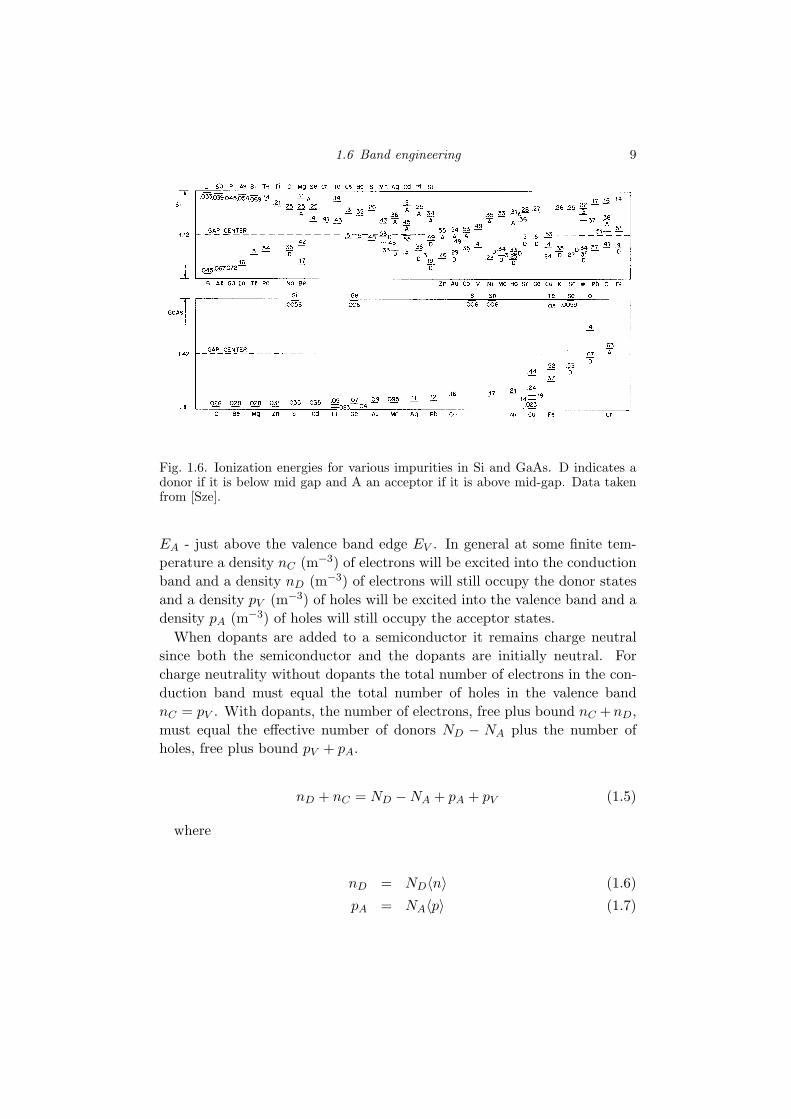
A three-dimensional electron or hole gas can be created in a semiconduc-tor by doping it with impurities. For example, a group IV semiconductorwith group III dopants has occasional bonds with missing electrons. At fi-nite temperatures valence electrons become excited and fill some of theselocalized holes leaving behind de-localized holes in the valence band. Thesecarriers are then free to propagate through the semiconductor and give riseto free-electron-like hole conductivity. We consider two generic types of im-purity: donor impurities; and acceptor impurities. Both contribute states inthe band gap of a semiconductor. Donor impurity states typically lie closeto the conduction band edge (Fig 1.6) and contribute conduction electrons.An intrinsic semiconductor doped with donor impurities is called an n-typesemiconductor. Acceptor impurity states typically lie close to the valenceband edge (Fig 1.6) and contribute holes to the conduction process. Anintrinsic semiconductor doped with acceptor impurities is called a p-typesemiconductor.
Three-dimensional electron or hole gases made by doping semiconductorsare not ideal for studying quantum effects for two reasons: they are stronglydisordered owing to the background of ionized impurities; and most quan-tum effects are more pronounced in lower-dimensional systems. Therefore,we will look at ways in which two-dimensional or lower dimensional electronor hole gases can be made in semiconductors. This is achieved through ‘bandengineering’. There are two principal parts to band engineering: modifica-tion of the chemical potential and carrier densities; and bending bands withunbalanced charge.
1.6 Band engineering
1.6.1 Modification of chemical potential and carrier densities
Fig. 1.7 shows an idealised doped semiconductor with an acceptor concen-tration NA (m−3) and donor concentration ND (m−3). The donor statesform a narrow band of energies around energy ED - just below the conduc-tion band edge EC . The acceptor states form a narrow band around energy
1.6 Band engineering 9
Fig. 1.6. Ionization energies for various impurities in Si and GaAs. D indicates adonor if it is below mid gap and A an acceptor if it is above mid-gap. Data takenfrom [Sze].
EA - just above the valence band edge EV . In general at some finite tem-perature a density nC (m−3) of electrons will be excited into the conductionband and a density nD (m−3) of electrons will still occupy the donor statesand a density pV (m−3) of holes will be excited into the valence band and adensity pA (m−3) of holes will still occupy the acceptor states.
When dopants are added to a semiconductor it remains charge neutralsince both the semiconductor and the dopants are initially neutral. Forcharge neutrality without dopants the total number of electrons in the con-duction band must equal the total number of holes in the valence bandnC = pV . With dopants, the number of electrons, free plus bound nC + nD,must equal the effective number of donors ND − NA plus the number ofholes, free plus bound pV + pA.
nD + nC = ND −NA + pA + pV (1.5)
where
nD = ND〈n〉 (1.6)
pA = NA〈p〉 (1.7)

10 The Free Electron Gas
µ
ND
NA
EC
nC
EV
EA
ED
nD
pA
pVE
z
Fig. 1.7. Definitions of electron and hole densities and energies.
〈p〉 is the average number of holes occupying each acceptor state and 〈n〉is the average number of electrons occupying each donor state. Their func-tional forms are derived in Appendix I. They predict a lower occupation thanFermi-Dirac statistics owing to the Coulomb repulsion entailed in multipleoccupation of localized impurity states,
The free carrier densities nC and pV are determined by Fermi statisticsthrough
nC =∫ ∞
EC
gC(ε)f(ε)dε (1.8)
pV =∫ EV
−∞gV (ε)(1− f(ε))dε (1.9)
where gC(ε) and gV (ε) are the conduction-band and valence-band densitiesof states, (derived for a spherical Fermi surface in Appendix II) and f(ε)is the Fermi-Dirac distribution function (Appendix I). The set of coupledequations [1.5] → [1.9] have as input NA, ND, EC−EV , ED, EA, m∗, and T
and can be solved for nC , nD, pA, pV and µ. Approximate solutions for thesequantities are derived in many text books [Ashcroft and Mermin, Kittel, Sze,Kelly] and exact solutions can be found numerically. The most importantresults from these solutions are that: the larger NA is, the closer µ is to EV
1.6 Band engineering 11
µ
E
z
µ
Fig. 1.8. (a) n-type semiconductor (b) p-type semiconductor
and the greater pV is; and the larger ND is, the closer µ is to EC and thegreater nC is.
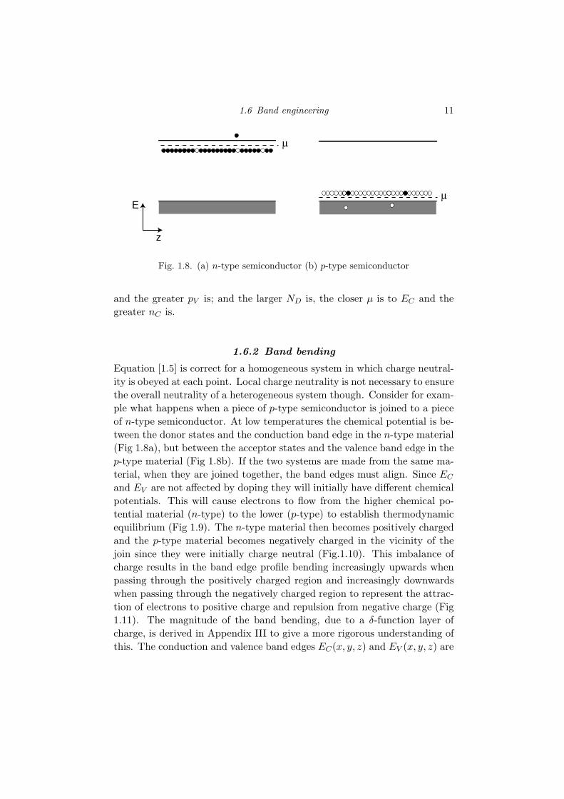
1.6.2 Band bending
Equation [1.5] is correct for a homogeneous system in which charge neutral-ity is obeyed at each point. Local charge neutrality is not necessary to ensurethe overall neutrality of a heterogeneous system though. Consider for exam-ple what happens when a piece of p-type semiconductor is joined to a pieceof n-type semiconductor. At low temperatures the chemical potential is be-tween the donor states and the conduction band edge in the n-type material(Fig 1.8a), but between the acceptor states and the valence band edge in thep-type material (Fig 1.8b). If the two systems are made from the same ma-terial, when they are joined together, the band edges must align. Since EC
and EV are not affected by doping they will initially have different chemicalpotentials. This will cause electrons to flow from the higher chemical po-tential material (n-type) to the lower (p-type) to establish thermodynamicequilibrium (Fig 1.9). The n-type material then becomes positively chargedand the p-type material becomes negatively charged in the vicinity of thejoin since they were initially charge neutral (Fig.1.10). This imbalance ofcharge results in the band edge profile bending increasingly upwards whenpassing through the positively charged region and increasingly downwardswhen passing through the negatively charged region to represent the attrac-tion of electrons to positive charge and repulsion from negative charge (Fig1.11). The magnitude of the band bending, due to a δ-function layer ofcharge, is derived in Appendix III to give a more rigorous understanding ofthis. The conduction and valence band edges EC(x, y, z) and EV (x, y, z) are

12 The Free Electron Gas
µp
nµ
Flow of electrons
E
z
Fig. 1.9. n− p junction before equilibration.
ρ
p - typen - type
+
- Z
Fig. 1.10. Charge density distribution ρ in a n− p junction.
the position dependent effective electrostatic potential energies of free elec-trons and free holes respectively. An electron placed in the conduction bandof Fig. 1.11 will accelerate downhill moving to the left (an = −∇EC/m∗
n),and a hole placed in the valence band of Fig. 1.11 will accelerate uphillmoving to the right (ap = −∇EV /m∗
p).Once equilibrium is established in any electronic device the chemical po-
tential µ will be constant throughout. We will frequently choose µ as thepotential zero of the system in these notes. The general problem of cal-culating the equilibrium band edge profiles EC(x, y, z) and EV (x, y, z) andthe charge density distribution ρ(x, y, z) is numerically intensive since onecannot assume local charge neutrality, Eqn. [1.5], only global charge neu-

1.7 The Si metal-oxide-semiconductor junction 13
µ
E (z) C
E (z) V
E (z) + EV A
E (z) - EC D E
z
Fig. 1.11. n-p junction after equilibration.
trality. One must solve Poissons equation to find EC and EV in terms of ρ
the unbalanced charge density:
−∇2φ =ρ
ε(1.10)
φ =−EC
e(1.11)
EV = Ec −Eg (1.12)
ρ = e(ND −NA + pV + pA − nC − nD) (1.13)
For boundary conditions to Eqn. [1.10], the values of EC and EV on thesurface of the device can be chosen to be those obtained for bulk dopedmaterial. The potentials EC and EV are related to ρ through equations[1.6 - 1.9] and therefore the set of coupled equations [1.6-1.13] can be solvediteratively until self-consistent band profiles and densities are found.
We are now in a position to understand how to use selective dopingto make low-dimensional electron or hole gases in semiconductor materi-als through band engineering.
1.7 The Si metal-oxide-semiconductor junction
The Si metal-oxide-semiconductor (MOS) junction (Fig. 1.12) is a doubleplate capacitor consisting of a metal plate, a SiO2 insulating spacer layerand a Si plate. The states of a metal and a semiconductor align at the

14 The Free Electron Gas
Ws
Vacuum Level
S
CE
VE
µ
Si
SiO
2
Mµ
Metal
WM
E
z
Fig. 1.12. Metal-Oxide-Semiconductor junction. WM is the metal work functionand WS is the semiconductor work function.
Flow of
electrons
µp
µM
E
z
µ
Fig. 1.13. Metal-oxide-p-type semiconductor junction (a) Before equilibration (b)After equilibration.
vacuum level but, in general, have different work functions WM and WS .This results in them having different chemical potentials and therefore someequilibration and band bending will occur when a metal and a semiconductorare brought together. In Fig. 1.12 we have neglected this.
If the semiconductor in a MOS junction is p-type we will have WM < WS
and on contact charge will flow from the metal into the semiconductor toachieve equilibrium as shown in Figs. 1.13a,b. This creates a region ofunbalanced negative charge at the oxide-semiconductor interface giving riseto the band bending seen in Fig 1.13b.
If the semiconductor is n-type then WM > WS and on contact charge willflow from the semiconductor into the metal to achieve equilibrium as shown

1.7 The Si metal-oxide-semiconductor junction 15
µn
Flow of
electrons
E
z
µ
Fig. 1.14. Metal-oxide-n-type semiconductor junction. (a) Before equilibration (b)After equilibration.
in Figs. 1.14a,b. This creates a region of unbalanced positive charge at theoxide-semiconductor interface.
If a positive voltage is applied to the metal plate in Fig. 1.13b with respectto the substrate, the band edge profile in the vicinity of the surface gate willbe increasingly bent downward as more as more negative charge is attractedto metal surface gate, filling acceptor states. At some point the conductionband edge EC will dip below the chemical potential in the substrate and thesemiclassical Eqn. [1.8] would predict that the triangular well that forms atthe interface will fill with free conduction electrons Fig. 1.15.
Typically, at least for small surface-gate voltages, the width of triangu-lar well is approximately equal to the Fermi wavelength of the conductionelectrons and Eqn. [1.8] should not be used to calculate the well carrierdensity because it assumes zero Fermi wavelength. A quantum mechanicalequivalent to Eqn. [1.8] must be used. In the effective-mass approximation,the Schrodinger equation for the well region has the form
− h2
2m∗∇2ψ + ECψ = Eψ (1.14)
Which has solutions of the form
Ei,k =h2k2
2m∗ + Ei (1.15)
where k = (kx,ky) is the wave vector for free motion in the x, y plane.The energies Ei are the quantum well subband energies (Fig. 16) and maybe found by direct numerical computation.

16 The Free Electron Gas
µ
eVg
Free electrons
in conduction
band
states
E
z
Fig. 1.15. A positive gate bias on metal-oxide-semiconductor junction with a p-typesubstrate.
Fig. 1.16. Bound states in a triangular quantum well at an oxide- p-type semicon-ductor interface.
When only the lowest energy subband E0 is beneath the substrate chemi-cal potential the device will have a single dynamically two-dimensional elec-tron gas at the oxide-semiconductor interface. Having calculated E0 quan-tum mechanically it may then be regarded as the zero of potential energy forthe two-dimensional gas and therefore the two-dimensional carrier density

1.8 The GaAs-AlxGa1−xAs heterostructure 17
n2D (m−2) may be calculated from
n2D =∫ ∞
E0
g2D(ε)f(ε)dε (1.16)
where g2D is the two-dimensional density of states (see Appendix IV).The spatial dependence of the well carrier density nC(x, y, z) (m−3) canthen be calculated from n2D by noting that this two-dimensional densityis distributed in the interface region according to the probability density ofthe bound state E0. A two-dimensional hole gas may be made by applyinga negative voltage to the metal gate of a metal-oxide-n-type junction Fig.1.14.
1.8 The GaAs-AlxGa1−xAs heterostructure
In order to study quantum-mechanical effects in a two-dimensional electrongas it is necessary to make them as free from unintentional potential modula-tion as possible. The drawback with the metal-oxide-semiconductor junctionis that there are occupied dopant states in the oxide-semiconductor interfaceregion exactly where the two-dimensional system forms. In addition, the ox-ide barrier is not smooth and contains a high density of trapped charge sinceit is amorphous. The GaAs-AlxGa1−x heterostructure, shown in Fig. 17a,b,partly solves these problems: these heterostructures are grown by molecu-lar beam epitaxy [Kelly] and the interface region where the two-dimensionalelectron gas forms is flat to within a mono-layer with no trapped charge; andmodulation doping is used to place dopants hundreds of Angstroms awayfrom the interface to reduce their ability to scatter. Electrons in the donorregion in Fig. 1.17(a) are well above the bulk chemical potential and there-fore flow out to the surface and interface regions during equilibration. Aswith the metal-oxide-semiconductor junction a dynamically two-dimensionalelectron gas can form at the interface, here at the GaAs-AlGaAs interface, ifthe doping concentration and length scales are chosen correctly. Fig. 1.17(b)shows the badstructure after equilibration.
1.9 Capacitor model
The dependence of the carrier density n2D on surface-gate voltage for boththe metal-oxide-semiconductor junction and the GaAs-AlGaAs heterostruc-ture may be calculated from a simple capacitor model. One plate of thecapacitor is a metal surface gate and the other the two-dimensional electrongas. The capacitance of the device is approximately, C = εA/d where d is

18 The Free Electron Gas
Flow of
Electrons
AlGaAsGaAs
µ
µd
Two-dimensional
electron gas forms
here
Metallic surface gates
AlGaAs
GaAs
µ
d
E
z
Fig. 1.17. (a) GaAs-AlGaAs heterostructure before equilibration. (b) GaAs-AlGaAs heterostructure after equilibration.
the distance from the surface gate to the two-dimensional electron gas andA is the area of the device. If we substitute this into the capacitor equationQ = CVg we have
e∆n2DA =εA
d∆Vg (1.17)
for an electron gas, where ∆n2D is the change in carrier density of thetwo-dimensional electron gas caused by a change in gate voltage ∆Vg, thissimplifies to
∆n2D =ε
ed∆Vg (1.18)
For a hole gas we have
∆p2D = − ε
ed∆Vg (1.19)
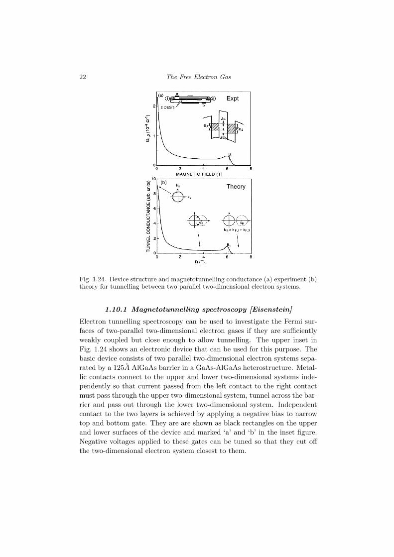
Figure 1.18 shows a typical GaAs-Al0.3Ga0.7As heterostructure device[Kardynal] and Fig. 1.19 shows how its carrier density n2D varies as afunction of both front and back gate voltages VFG,VBG. Figure 1.20 showshow the two-dimensional subband wave function and band edge vary as afunction of back-gate voltage.
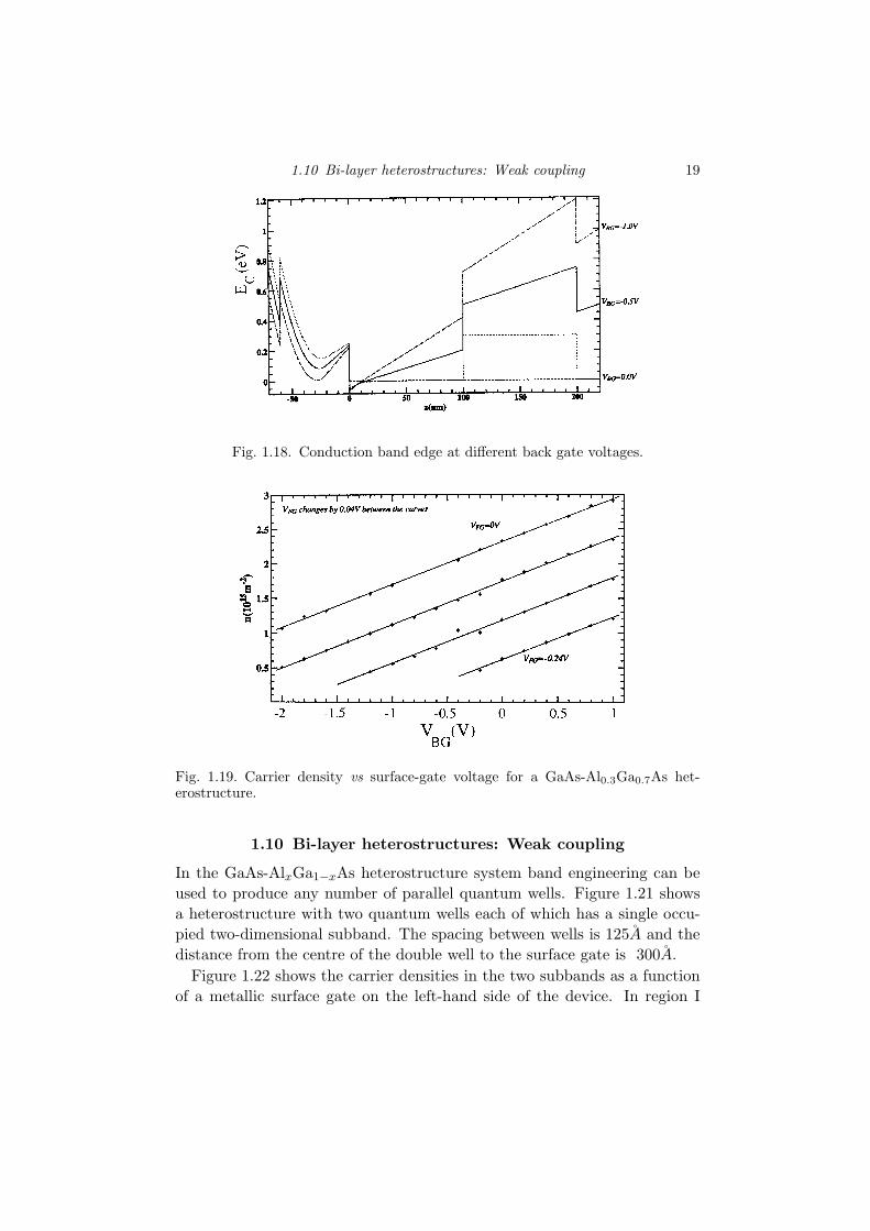
1.10 Bi-layer heterostructures: Weak coupling 19
Fig. 1.18. Conduction band edge at different back gate voltages.
Fig. 1.19. Carrier density vs surface-gate voltage for a GaAs-Al0.3Ga0.7As het-erostructure.
1.10 Bi-layer heterostructures: Weak coupling
In the GaAs-AlxGa1−xAs heterostructure system band engineering can beused to produce any number of parallel quantum wells. Figure 1.21 showsa heterostructure with two quantum wells each of which has a single occu-pied two-dimensional subband. The spacing between wells is 125A and thedistance from the centre of the double well to the surface gate is 300A.
Figure 1.22 shows the carrier densities in the two subbands as a functionof a metallic surface gate on the left-hand side of the device. In region I

20 The Free Electron Gas
Fig. 1.20. Wave functions in quantum well in Fig. 1.18 at three different back-gatevoltages.
Schottky Gate
GaAs 17 nm
AlGaAs, Si-doped 200 nm
AlGaAs 60 nm
GaAs 18 nmAlGaAs 12.5 nm
GaAs 18 nm
AlGaAs, Si-doped 200 nm
AlGaAs 250 nm
AlGaAs (Graded) 100 nm
AlGaAs 80 nm
GaAs Buffer0 0.5 1 1.5 2
x 104
z (A)
0
200
400
600
V (
meV
)
Fig. 1.21. (a) Schematic of double well wafer structure (b) Conduction band edgeprofile of a typical double quantum well system in a GaAs-AlxGa1−xAs heterostruc-ture.
only the right quantum well is occupied. At point II the left quantum wellbecomes occupied and screens the effect of the surface gate on the right wellso that its carrier density remains approximately constant over the rest ofthe gate voltage range. In this range the carrier density in the front wellincreases approximately linearly.

1.10 Bi-layer heterostructures: Weak coupling 21
-0.4 -0.2 0 0.2 0.40
0.5
1
1.5
2x 10
15
Vg (V)
n (m
-2)
III
(1)(2) (3)
(4)
(5)(6)
Fig. 1.22. Carrier densities in the two quantum wells of Fig. 1.21 as a function ofthe left surface-gate voltage.
2500 3000 3500 4000 4500 5000 5500-100
0
100
200
300
400
500
600
z (A)
Ec
(m
eV
)
(1) (2) (3)
(4) (5) (6)
Fig. 1.23. Double quantum well wave functions and conduction band edge at dif-ferent surface gate voltages d = 125A.
Figure 1.23 shows the double well region and its wave functions at thegate voltages marked by stars in Fig. 1.22. Note how the bending of theconduction-band edge becomes more pronounced as more carriers enter thequantum wells. At the voltage where the two densities are equal, no anti-crossing is seen. This is because the barrier is sufficiently high/wide thatcoherence is not preserved in multiple scattering of electrons between wells.Conservation of momentum in passing between quantum wells is observedthough and can be used to carry out a kind of electron spectroscopy.
22 The Free Electron Gas
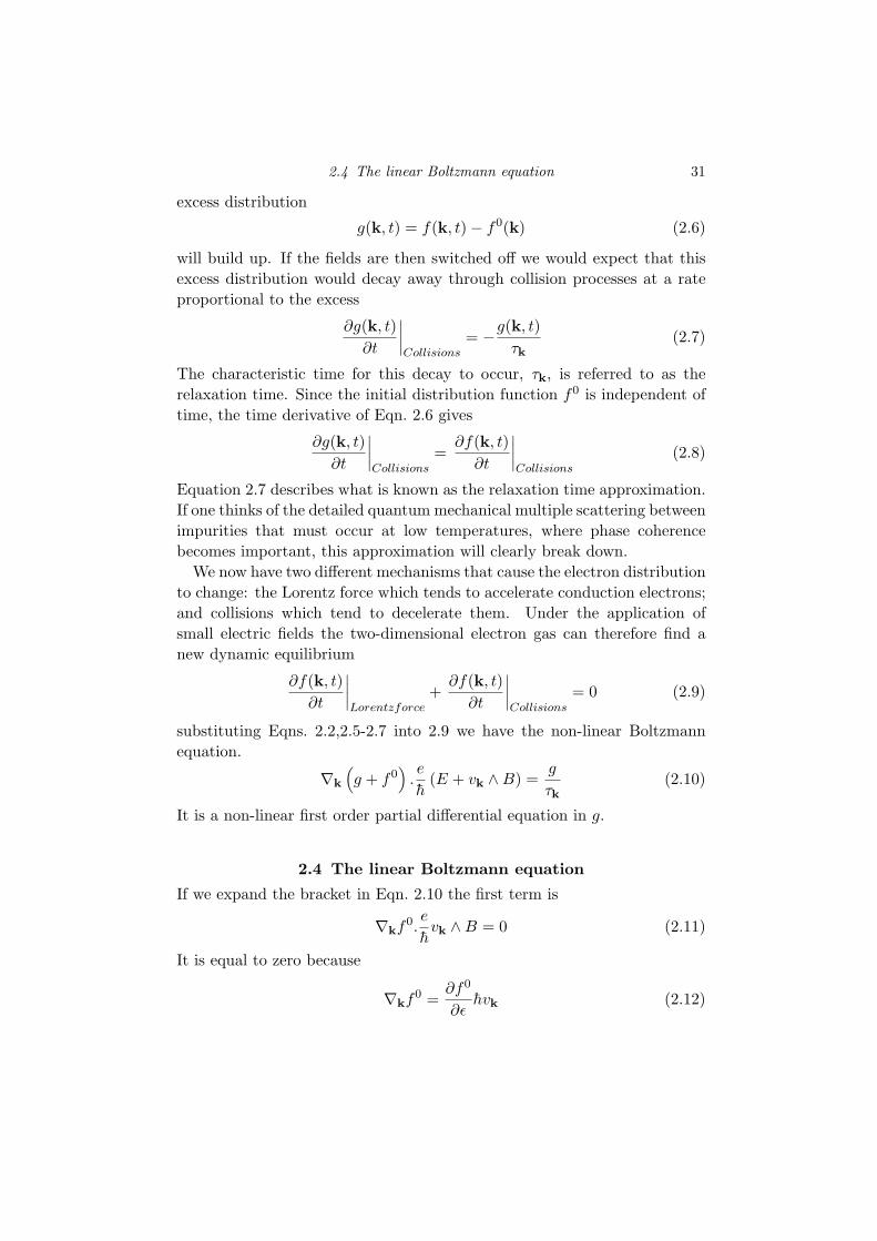
Expt
Theory(b)
Fig. 1.24. Device structure and magnetotunnelling conductance (a) experiment (b)theory for tunnelling between two parallel two-dimensional electron systems.
1.10.1 Magnetotunnelling spectroscopy [Eisenstein]
Electron tunnelling spectroscopy can be used to investigate the Fermi sur-faces of two-parallel two-dimensional electron gases if they are sufficientlyweakly coupled but close enough to allow tunnelling. The upper inset inFig. 1.24 shows an electronic device that can be used for this purpose. Thebasic device consists of two parallel two-dimensional electron systems sepa-rated by a 125A AlGaAs barrier in a GaAs-AlGaAs heterostructure. Metal-lic contacts connect to the upper and lower two-dimensional systems inde-pendently so that current passed from the left contact to the right contactmust pass through the upper two-dimensional system, tunnel across the bar-rier and pass out through the lower two-dimensional system. Independentcontact to the two layers is achieved by applying a negative bias to narrowtop and bottom gate. They are are shown as black rectangles on the upperand lower surfaces of the device and marked ‘a’ and ‘b’ in the inset figure.Negative voltages applied to these gates can be tuned so that they cut offthe two-dimensional electron system closest to them.

1.10 Bi-layer heterostructures: Weak coupling 23
A central metallic gate on the upper surface of the device can be used tochange the relative carrier densities in the two quantum wells and thereforecontrol tunnelling between the two-dimensional systems. The magnetotun-nelling experiment consists of measuring the equilibrium tunnelling differen-tial conductance dI/dV (I is the current passing between layers and V thepotential difference between layers) as a function of an externally appliedmagnetic field placed parallel to the two two-dimensional planes and alsoas a function of the relative carrier densities of the two systems. The term‘equilibrium’ here refers to the fact that the voltage V is made sufficientlysmall that it can be ignored in considering the individual properties of thetwo electron systems.
In equilibrium the two electron systems have the same chemical potentialbecause the barrier between the two quantum wells is sufficiently narrow toallow electrons to tunnel between the two quantum wells. This is shown inthe inset to figure [1.24]. At low temperatures the tunneling is restricted, byFermi statistics, so that it only occurs at the device chemical potential andtherefore between the Fermi surfaces of the two two-dimensional electronsystems. Tunnelling is further restricted by conservation of momentum andtherefore conservation of wavevector. The equilibrium tunnelling conduc-tance of the device is then given by the overlap integral of the Fermi-surfacespectral densities of the two-two-dimensional electron systems.
The wave functions in a two-dimensional system are plane waves
Ψkx,ky = eikxxeikyy (1.20)
and have a dispersion of the form
Ekx,ky =h2
2m∗(k2
x + k2y
)(1.21)
Hence, at the Fermi surface where Ekx,ky = EF there is only finite spectraldensity on a ring with k2
F = k2x + k2
y, where kF is the Fermi wave vector, asshown in Fig. 1.25.
The effect of a parallel magnetic field is to shift the two spectral functionsrelative to one-another in k-space. Schrodinger’s equation in a magneticfield has the form
(p + eA)2
2m∗ Ψ + V Ψ = EΨ (1.22)
In a parallel magnetic field B = (Bx, By, 0) we can use the Landau gauge forthe vector potential A = (Byz,−Bxz, 0). Substituting this into Eqn. 1.22

24 The Free Electron Gas
k x
k y
0
Fig. 1.25. Spectral density of a two-dimensional electron gas at its Fermi energy -the Fermi circle.
we get(
(px + eByz)2
2m∗ +(py − eBxz)2
2m∗ +p2
z
2m∗
)Ψ + V Ψ = EΨ (1.23)
For the device in Fig. 1.24, centering the upper two-dimensional systemat z = 0 and the lower two-dimensional system at z = −d the respectiveSchrodinger equations have the form
(p2
x
2m∗ +p2
y
2m∗ +p2
z
2m∗
)Ψ + V Ψ = EΨ (1.24)
((px − eByd)2
2m∗ +(py + eBxd)2
2m∗ +p2
z
2m∗
)Ψ + V Ψ = EΨ (1.25)
so that their k-space origins are offset by
px → px − eByd ⇒ kx → kx − eByd
h(1.26)
py → py + eBxd ⇒ ky → ky +eBxd
h(1.27)
The form of the traces in figures [1.24] and [1.26] can readily understoodin terms of a model consisting of the overlap between the two Fermi surface

1.11 Bi-layer heterostructures: Strong coupling [Davies] 25
(a) Expt
Theory
Fig. 1.26. Magnetotunnelling conductance (a) experiment (b) theory for tunnellingbetween two parallel two-dimensional electron systems as a function of their relativecarrier densities at different parallel field strengths.
rings of two two-dimensional electron gases. The theory (b) parts to eachof these figures show examples of the relative positions of the two Fermisurfaces.
1.11 Bi-layer heterostructures: Strong coupling [Davies]
Figure 1.27 shows the dependence of the quantum well carrier densities atthree different barrier thicknesses d = 125A, d = 45A and d = 25A. Asthe barrier thicknesses are made smaller a clear anti-crossing is observed.This is because multiple scattering begins to become coherent and the thestates in the two quantum wells begin to hybridize as they are brought closertogether and electrons are able to tunnel faster.
The wave functions and eigenenergies for the 25A case are shown in Fig.1.28 at a series of different surface gate voltages.

26 The Free Electron Gas
– 0.6 – 0.4 – 0.2 0 0.20
0.5
1.0
1.5
Vf (V)
n1, n
2 (
101
5 m
–2 )
0
1.0
2.0
3.0
n =
n 1 +
n 2
(10
15
m–
2)
n1
n2
n
25Å
nf
nb
– 0.6 – 0.4 – 0.2 0 0.20
0.5
1.0
1.5
2.0
Vf (V)
nf,
n
b (
101
5 m
–2 )
0
1.0
2.0
3.0
4.0
n =
n f + n
b (1
01
5 m
–2)
n
125Å
– 0.6 – 0.4 – 0.2 0 0.20
0.5
1.0
1.5
2.0
Vf (V)
0
1.0
2.0
3.0
4.0
n1
n2
n
45Ån
1, n
2 (
101
5 m
–2 )
n =
n 1 +
n 2
(10
15
m–
2)
Fig. 1.27. Carrier densities of of front and back quantum wells in three differentbi-layer heterostructure plotted as a function of surface gate voltage.
I
II
III
IV
-0.6 -0.4 -0.2 0 0.2
-6
-4
-2
0
Su
bb
and
En
erg
ies
(meV
)
III-eV
f
Vf (V)
IIIVI
-eVf
-eVf -eV
f
∆SAS
Fig. 1.28. Strongly coupled double quantum-well wave-functions and energies as afunction of surface-gate voltage d = 25A.

1.12 Exercises 27
1.12 Exercises
1.1 In what way is motion of an electron in free space similar/differentfrom motion of conduction electrons or holes in intrinsic semicon-ductors.
1.2 Describe qualitatively how the chemical potential, carrier densities,unionized donor and acceptor concentrations vary as a function ofND , NA and temperature in a semiconductor.
1.3 How is equilibrium established when a p− n junction is formed.1.4 What is meant by band bending in semiconductors and why does it
occur.1.5 Describe how a two-dimensional hole gas may be created in a Si
MOSFET.1.6 In what way is a two-dimensional electron or hole gas in a MOSFET
dynamically two-dimensional.1.7 Describe the different aspects of band engineering that go into mak-
ing a GaAs-AlGaAs heterostructure.1.8 If a square quantum well in a GaAs-AlGaAs heterostructure has a
width of 150A. what is the difference in energy between the loweststate of the well and the next.
1.9 If a quantum well in a GaAs-AlGaAs heterostructure, containinga single two-dimensional electron gas, has a Fermi energy of 10meVwhat is the carrier density. If the distance between the two-dimensionalelectron gas and a metal surface gate is 300nm what would thechange in carrier density be for a change in gate voltage of 1 Volt.
1.10 The device shown in Fig. 1.17(b) has a problem for practical appli-cations since the AlGaAs at the left surface would be likely to oxidiseand therefore destroy the device. Design an alternative device thatwould be more practical.

2
Semi-classical electron transport.
2.1 Reference material
[A M] Solid State Physics, N. W. Ashcroft and N. D. Mermin.[Ziman] Principles of the Theory of Solids, J. M. Ziman.
2.2 Introduction
Now that we have understood some of the general physics of two-dimensionalsystems in semiconductors it is natural to ask about their general transportcharacteristics. We will begin this process by looking at the predictions ofa powerful semiclassical theory: Boltzmann transport theory.
In this section we derive the semi-classical Boltzmann equation for thetwo-dimensional case and use it to understand electronic transport in two-dimensional electron systems containing many scattering centers. The Boltz-mann equation expresses transport dynamics in these systems in terms ofa balance between acceleration, due to the Lorentz force, and deceleration,due to collisions with the scattering centers.
2.3 The non-linear Boltzmann equation
We consider a two-dimensional electron system confined to the x− y plane.If this system is in equilibrium and there are no electric or magnetic fieldspresent the electrons will be distributed according to the Fermi-Dirac func-tion:
f0(k) =1
1 + exp(
εk−µkBT
) . (2.1)
28

2.3 The non-linear Boltzmann equation 29
kx
ky
0
Fig. 2.1. k-space of a two-dimensional electron gas showing occupied Fermi circle.
At low temperature the occupied states fill the Fermi circle, which is centredaround k = (kx, ky) = 0, as shown Fig. 2.1. This distribution has no netmomentum and therefore no net current flows.
When electric and magnetic fields E, B are switched on, electrons passingthrough the system will be accelerated by the Lorentz force. An electroninitially in a state k with velocity vk will receive an acceleration
dvk
dt=
h
m∗dkdt
= − e
m∗ (E + vk ∧B) (2.2)
This acceleration will cause the electron distribution f to evolve in timef → f(k, t). The distribution function f(k, t)d2k/(2π)2 is defined as, theaverage number of electrons occupying the infinitesimal volume of k-spaced2k around wave vector k at time t. We can quantify the evolution of f ifwe think of the acceleration dk/dt as a velocity in k-space. This conceptis illustrated in Fig. 2.2. Any electrons occupying a small volume of k-space around wave vector k, box 1 in Fig. 2.2, with velocity k at time t
will move so that they are in a small volume of k-space around wave vectork′ = k + kdt, box 2 in Fig. 2.2, at time t + dt. This implies that
f(k, t) = f(k + kdt, t + dt) (2.3)
If we now assume: that the change in f is a small perturbation on f0; andthat the application of small magnetic and electric fields will not alter the

30 Semi-classical electron transport.
Box 1
Box 2k
0
t+dt
t
k'=k +kdt
ky
kx
k
Fig. 2.2. Motion in k-space due to the Lorentz Force.
eigen spectrum of the two-dimensional system significantly - we will comeback to this in a later lecture - we can make a Taylor expansion of Eqn. 2.3.To first order in dt this is:
≈ f(k, t) +∇kf.kdt +∂f
∂tdt
0 = ∇kf.k +∂f
∂t(2.4)
so that the rate of change of f with respect to time from the Lorentz forcehas the form
∂f
∂t
∣∣∣∣Lorentzforce
= −∇kf.k (2.5)
If the acceleration of electrons in the system ran unchecked by any mech-anism, the assumption that the new distribution function is a small per-turbation on the zero field distribution would certainly be wrong. In realsystems there are many compensating factors: (1) Electrons may scatterfrom impurities or crystal defects. At low temperatures this is typically thedominant mechanism. (2) They can scatter from phonons. This mechanismbecomes dominant at higher temperatures. (3) They can collide with eachother since they are charged particles. We will discuss this in more detaillater in lectures.
After switching on the electric and magnetic fields for a short time an
2.4 The linear Boltzmann equation 31
excess distribution
g(k, t) = f(k, t)− f0(k) (2.6)
will build up. If the fields are then switched off we would expect that thisexcess distribution would decay away through collision processes at a rateproportional to the excess
∂g(k, t)∂t
∣∣∣∣Collisions
= −g(k, t)τk
(2.7)
The characteristic time for this decay to occur, τk, is referred to as therelaxation time. Since the initial distribution function f0 is independent oftime, the time derivative of Eqn. 2.6 gives
∂g(k, t)∂t
∣∣∣∣Collisions
=∂f(k, t)
∂t
∣∣∣∣Collisions
(2.8)
Equation 2.7 describes what is known as the relaxation time approximation.If one thinks of the detailed quantum mechanical multiple scattering betweenimpurities that must occur at low temperatures, where phase coherencebecomes important, this approximation will clearly break down.
We now have two different mechanisms that cause the electron distributionto change: the Lorentz force which tends to accelerate conduction electrons;and collisions which tend to decelerate them. Under the application ofsmall electric fields the two-dimensional electron gas can therefore find anew dynamic equilibrium
∂f(k, t)∂t
∣∣∣∣Lorentzforce
+∂f(k, t)
∂t
∣∣∣∣Collisions
= 0 (2.9)
substituting Eqns. 2.2,2.5-2.7 into 2.9 we have the non-linear Boltzmannequation.
∇k
(g + f0
).e
h(E + vk ∧B) =
g
τk(2.10)
It is a non-linear first order partial differential equation in g.
2.4 The linear Boltzmann equation
If we expand the bracket in Eqn. 2.10 the first term is
∇kf0.e
hvk ∧B = 0 (2.11)
It is equal to zero because
∇kf0 =∂f0
∂εhvk (2.12)

32 Semi-classical electron transport.
kx
ky
0∆k
Fig. 2.3. Shift of the Fermi circle owing to external electric field ∆k = −eτE/h.
and vk.vk ∧B = 0. The second term is the non-linear term
∇kg.e
hE (2.13)
It is non-linear because it is a product of the electric field E and the excessdistribution g that the electric field produces. Removing these terms resultsin the linear Boltzmann equation:
∇kg.e
hvk ∧B +∇kf0.
e
hE =
g
τk(2.14)
It will be valid if the excess distribution g is small.In zero magnetic field the solution to the linear Boltzmann equation is
trivial since the only term containing a derivative is multiplied by the mag-netic field B. The solution is:
g(k) =eτkh∇kf0.E (2.15)
substituting from Eqn. 2.6 we find
f = f0 +eτk
h∇kf0.E (2.16)
If we assume that the relaxation time τk is constant τk = τ equation 2.16yields a very simple picture of transport in a two-dimensional system. Wemay rewrite Eqn. 2.16 to the same order of approximation as
f = f0(k +
eτ
hE
)(2.17)
Equation 2.17 indicates that under the influence of an electric field the new

2.5 Semi-classical conductivity 33
dynamic equilibrium is represented by shifting the zero-field Fermi circle inthe opposite direction to the applied electric field (opposite since electroniccharge is negative) by an amount ∆k = −eτE/h in k-space. This is shownFig. 2.3. This shift may be viewed as each electron picking up an additionaldrift velocity vd owing to the influence of the electric field. This drift velocityis defined by
m∗vd
h= 4k = −eτE/h (2.18)
From this equation it is clear that the longer the relaxation time τ the largerthe drift velocity vd will be for a given electric field E. Using equation [2.18]the electron mobility µ can be written:
µ =|vd||E| =
eτ
m∗ (2.19)
(note that the same symbol µ is also used both for the chemical potentialEqn. 2.1 and for microns µm). Mobility is a measure of the purity of asystem. Good electron mobilities in GaAs-AlGaAs heterostructures are µ
= 50m2/Vs → 1000m2/Vs. This implies relaxation times of τ = 19 ps →380 ps and typical drift velocities in a low temperature measurement of |vd|= 0.6 ms−1 → 12.5 ms−1 assuming a 1mV potential difference across an80µm sample.
2.5 Semi-classical conductivity
We can use the functional form of the equilibrium excess distribution Eqn. 2.15to calculate the conductivity of a two-dimensional system containing scatter-ing centers. The equilibrium distribution function f(k) represents a dynamicequilibrium in which a current is flowing through the system. This currentis given by
j = 2∫ d2k
(2π)2.− evkf (2.20)
We include a factor of two for spin degeneracy. In Si this would be a factorof four owing to the extra valley degeneracy. The twelvefold bulk degeneracyis reduced to four at the SiO2 Si interface. The term d2k/(2π)2 in Eqn. 2.20is the density of states within an infinitesimal volume of k-space.
Since there is no current flow in zero field Eqn. 2.20 may be written
j = 2∫ d2k
(2π)2.− evkg (2.21)

34 Semi-classical electron transport.
substituting for g from Eqn. 2.15 we find
j =2e2
(2π)2
∫d2k
(−∂f0
∂ε
)τkvk(vk.E) (2.22)
which may be rewritten as
j = σ.E (2.23)
where σ is the conductivity tensor (a 2x2 matrix)
σ =2e2
(2π)2
∫d2k
(−∂f0
∂ε
)τkvk ⊗ vk (2.24)
(Mathematical notation - outer product of two vectors a , b is written (a⊗b)i,j = aibj . In our case vk is a 1x2 vector and so vk ⊗ vk is a 2x2 matrix).If the functional form for τk is known equation Eqn. 2.24 can be integratedto find the conductivity of a twodimensional system with arbitrary shapeFermi surface.
For this lecture course, the important thing about Eqn. 2.24is that thederivative of the Fermi-Dirac distribution −∂f/∂ε appears in the integrand.Its presence implies that, even though we know that every electron haspicked up the same additional drift velocity vd irrespective of its energyor wave vector, at low temperatures it is only those states that are at theFermi-surface that contribute to the conductivity.
Electrons at the Fermi-surface of a two-dimensional electron gas travelat phenomenal velocities. For example with a typical Fermi energy ofEF =10meV in a GaAs-AlGaAs heterostructure the Fermi velocity will bevF =280000ms−1. For the relaxation times τ =19ps → 380ps this impliesthe mean free path for electrons at the Fermi surface is lF = vF t = 5.3µm106µm. With modern lithographic techniques making electronic devicessmaller than this has become standard. We will look at ballistic motion ofelectrons in such devices in the next part of the notes.
2.6 Drude conductivity
Equation Eqn. 2.24 reduces to the Drude formula for conductivity if we as-sume a constant relaxation time, zero temperature and a parabolic disper-sion relation ε = h2k2/2m∗. Rewriting the integral Eqn. 2.22 in cylindricalco-ordinates in k-space we have
j =2e2τ
(2π)2
∫kdkdφ
(−∂f0
∂ε
)(vk cos(φ)kx + vk sin(φ)ky) (vk cos(φ)Ex + vk sin(φ)Ey)
(2.25)

2.6 Drude conductivity 35
E0
EFµ
Fig. 2.4. Heterojunction interface with sub-band energy E0 and Fermi energy EF .
which expands to
j =2e2τ
(2π)2
∫kdkdφ
(−∂f0
∂ε
) (v2k cos2(φ)Exkx + v2
k sin2(φ)Eyky + cos(φ) sin(φ) (Exkx + Eyky))
(2.26)performing the integral over φ we have
j =2e2τ
(2π)2
∫kdk
(−∂f0
∂ε
)v2kπE (2.27)
In the limit of zero temperature the derivative of the Fermi-Dirac functionbecomes a delta function at the chemical potential µ. If we choose the zeroof potential energy to be at the two-dimensional sub-band energy E0 (shownin Fig. 2.4) then
limT → 0
(−∂f0
∂ε
)= δ(ε− EF ) (2.28)
The dispersion relation for the system is
ε =h2k2
2m∗ =12m∗v2
k (2.29)
dε =h2kdk
2m∗ (2.30)
Substituting Eqns. 2.28-2.30 into Eqn. 2.27 we have
j =2e2τ
(2π)2.m∗
h2
∫dεδ(ε−EF )
2ε
m∗πE (2.31)
36 Semi-classical electron transport.
θf(k)
1-f(k')k'
k
θ
f(k')
1-f(k)
k'
k
Fig. 2.5. Elastic scattering from an impurity (a) k → k′ (b) k′ → k.
which after some algebra gives
σ =e2τ
m∗ n2D = eµn2D (2.32)
where n2D is the carrier density of the two-dimensional electron gas. Thisexpression is often misinterpreted as implying that conductivity derives fromall occupied states. As we have seen, this is not the case at low temperature,only states at the Fermi surface contribute.
2.7 Impurity scattering
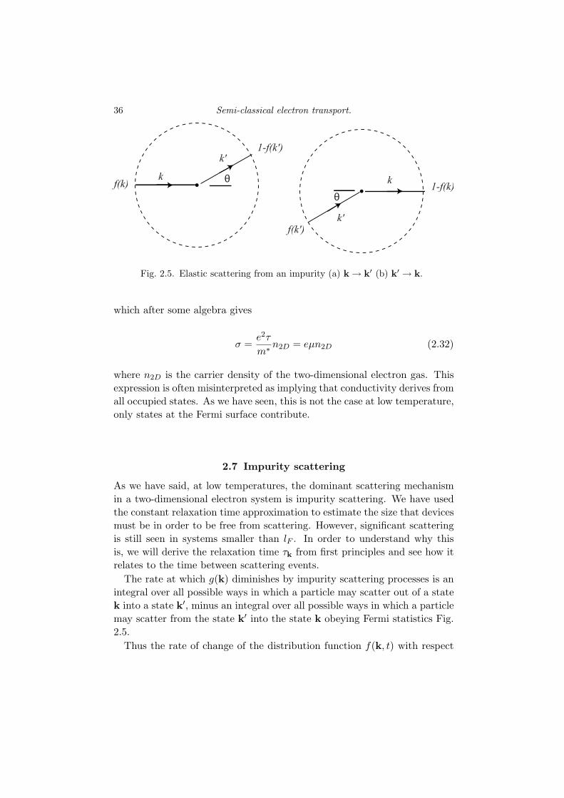
As we have said, at low temperatures, the dominant scattering mechanismin a two-dimensional electron system is impurity scattering. We have usedthe constant relaxation time approximation to estimate the size that devicesmust be in order to be free from scattering. However, significant scatteringis still seen in systems smaller than lF . In order to understand why thisis, we will derive the relaxation time τk from first principles and see how itrelates to the time between scattering events.
The rate at which g(k) diminishes by impurity scattering processes is anintegral over all possible ways in which a particle may scatter out of a statek into a state k′, minus an integral over all possible ways in which a particlemay scatter from the state k′ into the state k obeying Fermi statistics Fig.2.5.
Thus the rate of change of the distribution function f(k, t) with respect

2.7 Impurity scattering 37
to time can be written as
∂f(k, t)∂t
∣∣∣∣Collisions
= −∫ d2k
(2π)2[Wk,k′f(k)(1− f(k′)−Wk′,kf(k′)(1− f(k))
]
(2.33)The factor f(k)(1− f(k′)) is the probability, that the state k is occupied
and that the state k′ is unoccupied - the necessary condition for an electronin state k to be able to scatter into a state k′. The factor f(k′)(1 − f(k))is the probability for the reverse process Fig. 2.5(b). At low temperaturethese factors restrict scattering to the vicinity of the Fermi surface.
Wk,k′d2k′/(2π)2 is the probability per unit time that an electron in a statek will be scattered into an infinitesimal volume d2k′ around the state k′.This probability may be derived from Fermi’s Golden rule. The principal re-sults of such a derivation are that: the scattering event is symmetric Wk,k′ =Wk′,k; that energy is conserved in the collision |k|2 = |k′|2; that Wk,k′ is aneven function of only the angle between k and k′ Wk,k′ = W (k.k′/|k|2); andthat Wk,k′ is proportional to the density of impurity centers. Under theseassumptions Eqn. 2.33 simplifies to
g(k)τk
=∫ d2k
(2π)2Wk,k′(g(k)− g(k′)) (2.34)
after substituting for the left-hand side from Eqn. 2.6. For a large diffu-sive system we can assume that the relaxation time is isotropic τk = τ|k|.Substituting this into Eqn. 2.15 and rearranging we have
g = eτ|k|
(∂f0
∂ε
)vk.E = h
eτ|k|m∗
(∂f0
∂ε
)E.k = a(ε).k (2.35)
If we now substitute Eqn. 2.35 into Eqn. 2.34 we have
a(ε).kτ
= a(ε).∫ d2k
(2π)2Wk,k′(k− k′) (2.36)
Next we resolve k′ into components parallel k to k and perpendicular k⊥ tok Fig. 2.5.
k′ = |k′| cos(θ)k + |k′| sin(θ)k⊥ (2.37)
which, since energy is conserved in the collision, becomes
k′ = cos(θ)k + |k| sin(θ)k⊥ (2.38)
If we substitute Eqn. 2.38 into Eqn. 2.36, noting that Wk,k′ is an evenfunction of the angle θ between k and k′, we find an expression for the

38 Semi-classical electron transport.
relaxation rate1τk
=∫ d2k
(2π)2Wk,k′(1− cos(θ)) (2.39)
This result shows that the relaxation rate is a type of average over scatteringevents that gives little weight to forward scattering since the factor 1−cos(θ)is small for small θ. Therefore, if each scattering event itself is dominatedby forward scattering, as is the case for electrons in a two-dimensional elec-tron system scattering from impurity centers, the relaxation rate will remainsmall even if the rate at which scattering events occur is high. Hence, themean free paths lF calculated from lF = vF t above should only be takenas upper limits and not the distance between scattering events. They aremeasures of the distance through which electrons travel before suffering acollision that affects the bulk conductivity - large angle scattering. Equa-tion 2.39 demonstrates two further features of impurity scattering. The re-laxation rate is independent of temperature. It was eliminated in cancelinga(ε) from both sides of Eqn. 2.36. This explains why it becomes dominant atlow temperatures, since all other scattering mechanisms diminish with de-creasing temperature. We also find that the relaxation rate is proportionalto the density of scattering centers.
2.8 Exercises
2.1 Write a list of the assumptions that have gone into the derivationof the linear Boltzmann Eqn. 2.14. Suggest ways in which a fullyquantum mechanical formulation of the transport problem wouldhave to be different.
2.2 The expression for the Boltzmann conductivity Eqn. 2.24 containsthe derivative of the Fermi function in its integrand. How do you rec-oncile this with the fact that all electrons are equally affected by theapplication of an external electric field. What are the implicationsof this for low temperature electron transport.
2.3 Explain the distinction between the relaxation time and the timebetween scattering events within the Boltzmann formalism. What isthe distinction between the mean free path and the distance betweenscattering events.

3
Particle-like motion of electrons
3.1 Sources
[1] L. W. Molenkamp et al Phys. Rev. B 41 1274 (1990).[2] J. Spector et al, Appl. Phys. Lett. 56 967 (1989).[3] C. J. B. Ford et al, Phys. Rev. Lett 62 2724 (1989).[4] C. M. Marcus et al, Phys. Rev. Lett 69 506 (1992), ibid 74 3876
(1995).[5] J. Spector et al, Appl. Phys. Lett. 56 2433 (1990).[6] J. Spector et al, Appl. Phys. Lett. 56 1290 (1990).
3.2 Introduction
These notes look at particle-like (ballistic) motion of electrons in high-mobility two-dimensional electron systems. In particular they concentrateon experiments that demonstrate electrons behaving in a similar way tophotons in geometric optics. They cover: sources of electrons - the ohmiccontact; the split-gate electron aperture; cyclotron motion; the detection ofclassical skipping orbits; the observation of chaotic motion; classical refrac-tion; and the operation of a ballistic prism and a ballistic lens.
3.3 The Ohmic contact
In order to measure the transport properties of an electron system in asemiconductor device some way of connecting it to macroscopic measure-ment equipment must be found. For a two-dimensional electron gas this istypically achieved by creating a local conducting n++ region that extendsfrom the device surface, where a wire may be connected, to the interfacewhere the electron system forms. For GaAs-AlGaAs heterostructures con-ducting contacts are made by evaporating a patch of metal alloy, sufficiently
39

40 Particle-like motion of electrons
AlGaAs
Si - AlGaAs
AlGaAs
GaAs
n n
n n
p - type S i
Fig. 3.1. (a) Ohmic contact in GaAs-AlGaAs heterostructure (b) In a Si-MOSFET.
large to be seen easily through a low power optical microscope, onto thesurface of the device and then heating it until the alloy melts and diffusesdown to the interface. This is shown in Fig. 3.1a. For a Si metal-oxide-semiconductor junction device the contacts are made by firing ion dopantsinto the surface: Fig. 3.1b. Typically, these contacts will make electricalconnection to a large two-dimensional region that then feeds into the low-dimensional system being measured. Such contacts are referred to as ohmiccontacts if their resistance is constant for small applied potential biases i.eif they obey Ohm’s law I = V/R. Good ohmic contacts will have a low aresistance to prevent power dissipation and unknown voltage drops.
An ohmic contact is typically large in comparison to the mean free path ofthe two-dimensional system it contacts, its presence creates a large numberof crystal defects and it is threedimensional. The exact way in which ohmiccontacts achieve electrical contact is a complicated issue and is still in debate.However, an ideal ohmic contact should act like a Fermionic version of ablack-body radiator, sending and receiving electrons equally at all energiesand in all directions according to Fermi statistics. For this reason, an ohmiccontact can be thought of as analogous to a diffuse light source (light bulb)in geometric optics.
3.4 The electron aperture
The geometric motion of photons in an optical experiment is immediatelyapparent if one places a small aperture in front of a strong light source. Thelinear path of the light is seen by the eye where dust scatters it. But howcould such an experiment be performed on electrons in a two-dimensionalelectron system? The ohmic contacts take the place of both sources anddetectors but how can we create an aperture?
As we have discussed in the first lecture, the carrier density in a two-

3.5 Cyclotron motion 41
dimensional electron system can be controlled by applying a potential dif-ference between a metallic surface gate and the system itself. It is a smallstep from this concept to the realization that if the surface gate is made smallit can control the electron density locally, either by depleting or enhancingthe electron system directly under the gate. Fig. 3.2a shows a schematicdiagram of the effect of applying a negative potential to a metallic split gateon the surface of a GaAs-AlGaAs heterostructure. The narrow channel thatforms acts like a small aperture connecting two two-dimensional regions.
3.4.1 The effective potential
The general effect of applying potentials to arbitrary surface-gates patternedon a two-dimensional electron system can be summed up in terms of the socalled position-dependent two-dimensional ’effective potential’. Fig. 3.2bshows the conduction-band edge both, under a metal surface gate (uppertrace), and away from it when a negative potential has been applied tothe gate. Under the gate, the lowest two-dimensional subband energy E0
is above the chemical potential µ = 0 and so no electrons will occupy thequantum well. Away from the gate E0 is below the chemical potential andso the quantum well will be occupied. In general the subband energy E0 willbe a function of position E0(x, y) and is referred to as the two-dimensional’effective potential’ it is actually the position-dependent effective conduc-tion band edge in region of the quantum well. Its position dependence isdetermined by the pattern of surface gates and the potentials applied tothem and may be calculated by solving Schrodinger’s equation selfconsis-tently with Poisson’s equation. We will come back to this when we considerone and zero-dimensional systems in later lectures.
3.5 Cyclotron motion
The electron aperture that we have just described can be used as part of anelectronic device to show that electrons in a two-dimensional electron gastravel ballistically but it cannot be done as simply as it can in an opticalexperiment. There are no useful analogies to dust or the human eye. Theelectron apertures are also stuck to the surface of the device and cannot bemoved during an experiment. This means that although apertures can bemade so that they sit on a straight line between a source and a detector,they cannot be moved so that it can be demonstrated that electrons onlytravel in a straight line. Electrons do however respond to external fields,

42 Particle-like motion of electrons
(a)(b)
Fig. 3.2. (a) Schematic of a metallic split gate’ on the surface of a heterostructure(b) The conduction-band edge under a metallic gate (upper) and away from ametallic gate (lower) when a negative potential is applied to the gate.
through the Lorentz force, and an external magnetic field can be used tobend the path electrons take.
In the absence of an electric field the Lorentz force on an electron in atwo-dimensional system is F = −ev ∧ B. Where v is the electron velocityand B the external magnetic field. Any component of the magnetic fieldparallel to the two-dimensional system will have no effect on the motion ofthe electron in the x− y plane since the resulting Lorentz force acts in thedirection of confinement. In order to study the effect of a magnetic fieldon the motion of an electron forced to move in a two-dimensional plane,we need only consider the effect of a perpendicular magnetic field B = Bz.From Newton’s second law its motion described by
F = −eBvyx + eBvxy (3.1)
Within the effective mass approximation, we can ignore the underlying crys-tal lattice in a semiconductor electron system if we take its effect into accountvia an effective mass m∗. Using this effective mass in equation [3.1] we find
vx = −eB
m∗ vy = −ωcvy (3.2)
vy = +eB
m∗ vx = +ωcvx (3.3)
ωc is referred to as the cyclotron frequency. Substituting [3.2] into [3.3]we find two independent differential equations that show that the electrons

3.5 Cyclotron motion 43
Fig. 3.3. Cyclotron motion of electrons injected into a two-dimensional system.
velocities execute simple harmonic motion.
vx = −ω2cvx (3.4)
vy = −ω2cvy (3.5)
As we saw in the previous section of the notes, the only electrons thatare detected in the conduction process are at the Fermi surface. So, for thedevice shown in Fig. 3.3, the boundary conditions at the source apertureare vx = VF and vy = 0. vF is the Fermi velocity. With these boundary con-ditions the solution for the position of an electron from [3.2,5] as a functionof time t will be
x =vF
ωcsin(ωct) (3.6)
y =vF
ωc(1− cos(ωct) (3.7)
This motion describes a circle x2 +(y−R)2 = R2 where R = vF /ωc is thecyclotron radius - this motion is known as ’cyclotron motion’.

44 Particle-like motion of electrons
3.6 Experiments
We will now look in detail at a series of experiments that demonstrate bal-listic motion of electrons. All of the experiments were performed at lowtemperatures 1K on devices patterned on GaAs-AlGaAs heterostructureswith a single two-dimensional electron system at the interface between theGaAs and the AlGaAs. The electron systems were of high quality with mo-bilities µ > 50 m2/Vs. Surface gates are numbered 1,2,3... etc. They havenegative voltages applied to them that are sufficiently large to deplete theelectron gas under them and therefore define their shape as barriers in thetwo-dimensional system. Ohmic contacts are lettered A,B,C ... etc and areeither connected to earth, a current source, a voltage source or a volt meter.
3.7 Detection of ballistic motion L. W. Molenkamp [1]
Fig. 3.4a shows a schematic diagram of the device used in an experiment byL. W. Molenkamp to detect ballistic motion. There is a source and detectoraperture set opposite each other, gates 1,2 and gates 3,4. Behind the sourceaperture is the source ohmic contact A and behind the detector aperture isthe detector ohmic contact C. A current IA is injected into the system fromA. Ohmic contact D is connected to ground and acts as a sink to all electronsirrespective of their ballistic path. The voltage VC on ohmic contact C isthen measured relative to that on B. The measured resistance (VC−VB)/IA
is shown in Fig. 3.4b as a function of external magnetic field.Electrons that travel ballistically from A to C cause an over pressure of
electrons at contact C with respect to contact B where electrons must ar-rive by very complicated diffusive paths. When a magnetic field is appliedballistic electrons no longer pass directly from A to C and therefore the po-tential difference between C and B diminishes: Fig. 3.4b. This experiment,is one of the most clear demonstrations of ballistic electron motion in a two-dimensional system. In the referenced paper [1] the authors also performnumerical simulations using a ray tracing program to find the expected re-sistance for different shape apertures: Fig. 3.4b insets. The lower dashedline shows the expected ballistic peak for a square aperture exit. Such anaperture sprays electrons in all directions and therefore shows a lower bal-listic peak than experiment. A series of dots that approximately follow theexperimental trace show the result for a smoothly varying exit.

3.8 Collimation 45
Fig. 3.4. (a) Device for detecting ballistic motion of electrons. (b) Solid line mea-sured resistance, Dashed line theory square exit, Dots theory smooth exit.
3.8 Collimation
When electrons pass through a narrow split-gate aperture they scatter fromthe electrostatically defined edges. These edges are typically very smoothand the reflection from them is elastic with angle of incidence equal to theangle of exit θ = θ′: Fig. 3.5.
Such reflection leads directly to collimation through two processes. (1)As electrons exit the aperture the effective potential reduces in value untilit reaches the bulk potential. This causes the electrons to accelerate. Fig.3.6a shows how such acceleration leads to collimation. (2) The exit of anaperture widens as it reaches the exit. Fig. 3.6b shows how this leads tocollimation.
3.9 Skipping orbits J. Spector [2]
Fig. 3.3 shows that for a sufficiently strong magnetic field ballistic electronsin the Molenkamp experiment [1] would not reach the opposite ohmic contactbut would end up skipping along the source aperture electrostatic boundary.Fig. 3.7 shows an experimental device used to demonstrate this.
Ohmic contacts E and F are earthed and current is injected from ohmiccontact B. When a negative magnetic field is applied to the device electronsfrom the source aperture in front of B skip along the boundary between Band A. If a multiple of the cyclotron diameter 2R is equal to the distance

46 Particle-like motion of electrons
Fig. 3.5. Reflection from a graded boundary.
between the two apertures electrons pass directly from B into A and anenhanced voltage is measured. If the diameter is too large or too smallelectrons miss the aperture in front of A and only the diffuse backgroundwill be measured. This process appears as the oscillatory signal in Fig. 3.7b(trace (a)) as a function of magnetic field. The last peak results from a pathwith nine reflections from the electrostatic edge and clearly demonstratesthe purity of the device being measured.
When the magnetic field is applied in the positive direction electrons aredeflected to the left and a single peak is seen, trace (b), in Fig. 3.7b. Itcorresponds to an orbit without any reflection. Orbits that cause electronsto reflect from ohmic contact C do not give rise to peaks in the voltage atD since they are either absorbed or scattered randomly.
3.10 The cross junction C. J. B. Ford [3]
The inset to Fig. 3.8(a) shows a schematic view of a cross surface-gatestructure made by Christopher Ford when a postdoc at IBM.
A current IA is injected into the cross from contact A and a potentialdifference VBC between contacts B and C is measured. The experimentaltrace in Fig. 3.8a shows RH = VBC/IA as a function of magnetic field. Atlow magnetic fields cyclotron motion causes enhanced scattering from the

3.11 Chaotic Motion C. M. Marcus [4] 47
Fig. 3.6. (a) Collimation owing to decreasing potential. (b) Collimation owingincreasing width.
exit boundary walls but no electrons are directed to contact B. At somecritical field the electrons are directly focused into contact B and a positiveRH is measured. Fig. 3.8b shows the result of removing the corners ofthe cross. In this device, at small fields the electrons can bounce from theflat surface on gate 2 and give an enhanced voltage at C i.e a negativeRH . RH becomes increasingly negative with increasing magnetic field untilthe cyclotron radius is sufficiently small that electrons can pass ballisticallydirectly from A to B, RH then becomes positive. Fig. 3.8c shows the resultof introducing an artificial impurity into the centre of the cross structure.The dashed line shows the result with no voltage on gate 5, giving a resultidentical to Fig. 3.8b, and the solid line with a negative voltage on gate 5.The deflection of the ballistic electrons by the impurity causes them to passpreferentially into contact B even at low fields.
3.11 Chaotic Motion C. M. Marcus [4]
Figure 3.9 shows two gate patterns for two different devices used by CharlesMarcus to investigate chaotic motion. In the upper panel of Fig. 3.9 theelectron micro-graph shows a stadium shaped device defined by surface gates( gates in White, electron gas in black). The lower panel shows a circularshaped device. Each shape has an entrance and exit aperture. The resistance

48 Particle-like motion of electrons
Fig. 3.7. (a) Experimental device used to demonstrate skipping orbits. (b) Uppertrace (a) elastic scattering from an electrostatic edge. Lower trace (b) inelasticscattering from an ohmic contact.
traces shown in Fig. 3.9 are a measure of whether electrons are reflected fromthe structure ( high resistance ) or pass through ( low resistance ). We willshow the direct relationship between resistance and reflection coefficientsin subsequent lectures. The resistance is shown as a function of magneticfield. Each trace consists of a large number of peaks and dips. Peaks occurat magnetic fields where electrons are, eventually, reflected from the deviceand dips occur where electrons are eventually passed through the device.This type of structure is a signature of chaotic ballistic motion. It is asimple exercise in ray tracing to convince yourself that for a complicatedscattering path around either object a slight change in magnetic field canmake the difference between a particle exiting from the left or right aperture.Figs. 3.10a,b show a refinement to the experiment in Fig. 3.9, for which, inaddition to changing the magnetic field it was possible to alter the shape ofthe confined region with the gate Vg Fig. 3.10a.
The grey scale plot in Fig. 3.10b shows random fluctuation in the conduc-tance of the device as a function of both parameters. It has the signatureof chaotic motion extreme sensitivity to boundary conditions.

3.12 Classical refraction 49
Fig. 3.8. Hall resistance RH of (a) Cross gate pattern. (b) Corners removed (c)Artificial impurity.
3.12 Classical refraction
We have been discussing a series of experiments performed on ballistic elec-trons in which they appear to behave quite classically. We might thereforenot expect to see anything like refraction in the same systems. However,

50 Particle-like motion of electrons
Fig. 3.9. (a),(b) shows two gate patterns in white. Resistance of (a) Stadium (b)Circle showing extreme sensitivity to boundary conditions.
there is a classical analogue to optical refraction. Consider a beam of elec-trons incident on a graded potential step: Fig. 3.11. When an electronpasses through the graded region in Fig. 3.11 a normal force acts only inthe y direction and therefore momentum in the x direction is conserved.
|vF | sin(θ) =∣∣v′F
∣∣ sin(θ′) (3.8)
Energy is conserved as the collision of the electron with the step is elastic.The electron travels across the step at the chemical potential and the twospeeds vF and v′F are equal to the Fermi velocities in the two regions. Thus

3.12 Classical refraction 51
Fig. 3.10. (a) Device structure. (b) Grey scale plot of conductance as a functionof B and Vg. (c) Histogram of conductance modulation in (b) showing normaldistribution.
[3.6] may be rewritten as
sin(θ)sin(θ′)
=
√n′2D
n2D(3.9)
where n2D is the carrier density in the Vg = 0 region and n′2D in the Vg < 0region.
Refraction in geometric optics is shown in Fig. 3.12. The wavefront of abeam of photons is always perpendicular to the direction of propagation sothat in place of [3.6] we have
∣∣v′∣∣ sin(θ) = |v| sin(θ′) (3.10)
Substituting for the refractive indices n = c/v,n′ = c/v′ in equation [3.8]

52 Particle-like motion of electrons
<
Fig. 3.11. Classical refraction - electrons in parallel paths remain at the same rel-ative positions.
we findsin(θ)sin(θ′)
=n′
n(3.11)
The important difference between [3.7] and [3.9] is that for electrons undera metal surface gate with a negative voltage on it n2D < n′2D and thereforeθ′ > θ , Fig. 3.11, whereas for light passing from air into glass n′ > n andtherefore θ′ < θ, Fig. 3.12. We will see how this affects the design of aballistic lens in the last section of these notes.
3.13 Refraction J. Spector [5,6]
Fig. 3.13 shows an electron micrograph of a device that Joe Spectorused todemonstrate classical refraction of electrons.
Electrons are injected from ohmic contact F and pass through a sourceaperture defined by gates 7,8. They then pass through a second aperture

3.14 Exercises 53
Fig. 3.12. Refraction in optics. The wavefront is always perpendicular to the di-rection of motion.
defined by 6,9 and stray electrons are caught by ohmic contacts G,E. Ad-ditional stray electrons are removed after 6,9 with ohmic contacts W. Gate5 is the active refractive gate, the refractive index of which is altered bychanging the voltage on it. The three traces (a), (b), (c) in Fig. 3.13b showthe potential measured on ohmic contacts A,B,C as a function of the voltageon gate 5. For the lowest density, most negative gate voltage, the angle ofdeflection is the greatest, ballistic electrons pass preferentially into contactA. Traces (a), (b) and (c) show the results of numerical simulations using aray tracing program.
We noted in the derivation of classical refraction that it was in the oppositesense to optical refraction. This has its ultimate application in Joe Spector’sballistic electron lens shown in Fig. 3.14 where a converging lens has thesame shape as an optical diverging lens.
3.14 Exercises
3.1 Explain the electrical principles behind the detection of ballistic elec-tron motion in a two-dimensional system. A magnetic focusing ex-

54 Particle-like motion of electrons
Fig. 3.13. (a) Pattern of device to demonstrate classical refraction (b) Solid lineexperiment, dashed theory.
periment is performed in two-dimensional electron gas with mobility100m2/Vs and carrier density 1.0x10¹⁵m−2 using two split-gate aper-tures 4µm apart along the same edge. At what magnetic fields dothe first four focusing peaks occur. What might limit the numberof peaks seen. How might you account for uneven peak heights.Assume m∗=0.067me in all questions.
3.2 Explain how a surface gate can be used to cause a local modulationin the charge density of a two-dimensional system. Explain how acollimated beam of electrons can be created. How are optical andclassical refraction different. A collimated beam of ballistic electronsin a two-dimensional electron gas of Fermi energy 10meV is normallyincident on one surface of a wedge shaped region of low density withFermi energy 5meV and internal angle θ=30 caused by a surfacegate. What will the angle of exit be referred to the angle of incidence.What application might such a device have and what factors mightlimit the speed of its operation.

3.14 Exercises 55
Fig. 3.14. (a) Ballistic electron lens (b) Ratio of detected Id to injected current Ie:solid line experiment, dashed line theory.

4
The quantum Hall and Shubnikov de Haas effects
4.1 Sources
[A+M] Solid State Physics, N. W. Ashcroft and N. D. Mermin.[Ziman] Principles of the Theory of Solids, J. M. Ziman.[Pudalov] P. Pudalov et al Sov. Phys. JETP 62 1079 (1985).[Smith] T. P. Smith et al Phys. Rev. B 32 2696 (1985).
4.2 Introduction
These notes look at the effect of a perpendicular magnetic field on the elec-tronic structure and transport properties of a two-dimensional electron sys-tem. We show that the semiclassical Boltzmann formalism fails to accountfor high magnetic field behaviour owing to the formation of a new set ofstates: the Landau levels. We show that their existence is consistent with anumber of experimental observations.
The notes cover: the prediction of the Boltzmann formalism in finitemagnetic field; the eigenstates of a two-dimensional electron system in amagnetic field; the density of electrons in a Landau level; disorder broad-ening of a Landau level; the oscillation of the Fermi energy; the oscillationof the capacitance; and the basic features of the Shubnikov de Haas andQuantum Hall effects.
4.3 Boltzmann prediction
As was shown in the second lecture, the linear Boltzmann equation at finitemagnetic field has the form:
∇kg.e
hvk ∧B +∇kf
0.e
hE =
g
h(4.1)
56

4.3 Boltzmann prediction 57
0kx
ky
kxkkkx
Fig. 4.1. The locus of the Hall vector Z as a function of magnetic field - black circle.
In the constant relaxation time approximation τk = τ its solution can bewritten in the form:
g(k) =eτ
h∇kf
0.Z (4.2)
where Z is the so called Hall vector:
Z =E +
(eτm∗
)B ∧ E +
(eτm∗
)2 (B.E) B
1 +(
eτm∗
)2B.B
(4.3)
This form for Z is derived by substituting Eqn. 4.2 into Eqn. 4.1 (see ap-pendix for details) to find the following relationship between E, B, andZ:
E = Z −(
eτ
m∗
)B ∧ Z (4.4)
and then inverting it to find Z.The solution Eqn. 4.2 for the distribution g(k) has the same functional
form as the zero field case, Eqn. 2.15, but with E replaced by Z. Theequilibrium occupation probability f(k) = g(k) + f0(k) is therefore also ashifted Fermi circle with ∆k = −(eτ/h)Z:
f = f0(
k +eτ
hZ
)(4.5)

58 The quantum Hall and Shubnikov de Haas effects
Fig. 4.1 is a graphical representation of Eqn. 4.4. It shows that the locusof the Hall vector Z with magnetic field is a circle. It also shows thatthe drift of the Fermi circle is made smaller in magnitude and increasinglyperpendicular to the electric field E with increasing magnetic field.
4.4 Conductivity
The derivation of the conductivity for the finite field case follows the sameset of equations as given in section 2.5 of lecture 2 but where relevant withE replaced by Z. Equation 2.32 becomes
j = σ0Z = n2DeµZ = n2De2τ
hZ (4.6)
Substituting Eqn. 4.6 into Eqn. 4.4 we find
E =j
σ0− eτ
m∗B ∧ j
σ0(4.7)
Since we are considering a two-dimensional system in a perpendicular mag-netic field : j = jxx + jyy, E = Exx + Eyy and B = Bz. With thesedefinitions, Eqn. 4.6 takes the form
(Ex
Ey
)=
( 1σ0
eτm∗
1σ0
B
− eτm∗
1σ0
B 1σ0
) (jx
jy
)(4.8)
so that
E = ρj =( 1
σ0
eτm∗
1σ0
B
− eτm∗
1σ0
B 1σ0
)j (4.9)
Where ρ is the resistivity tensor. Thus within the Drude formalism thediagonal resistivity ρx,x = 1/σ0 is independent of magnetic field whereas, theoff-diagonal resistivity ρx,y = B/en2D or Hall resistivity increases linearlywith magnetic field.
4.5 Experiment
The resistivity tensor of a two-dimensional electron system can be mea-sured using a Hall bar. Fig. 4.2 is a schematic diagram showing a Hallbar patterned into a GaAs-AlGaAs heterostructure. Its shape is definedas a mesa by etching away the heterostructure wafer containing the two-dimensional electron gas in the regions where it is not wanted. In mea-surements of the resistivity tensor, a current I is passed between ohmiccontacts S and D giving a current density jx = I/W . For the diagonalresistivity ρxx = Ex/jx the voltage between ohmic contacts A and B, VAB,

4.5 Experiment 59
Fig. 4.2. Hall bar mesa patterned in a heterostructure wafer. Ohmic contacts A-D,S
Fig. 4.3. The Hall and diagonal magnetoresistance of an n-type GaAs-AlGaAs het-erojuction for a source drain current of 25µA at 1.2K.
is measured to find Ex = VAB/L. For the Hall resistivity ρx,y = Ey/jx
the voltage between ohmic contacts A and C, VAC , is measured to findEy = VAC/W . Note that the Hall resistivity and Hall resistance are equalρxy = (VAB/W ) / (I/W ) = VAC/I = Rxy. Fig. 4.3 shows a measurement ofρxx and ρxy for a two-dimensional electron system, with carrier density n2D
= 5.6 x 10¹⁵ m−2, in a GaAs-AlGaAs heterostructure.At magnetic fields below B ∼ 0.5T it is clear that the assumptions of
the Boltzmann formalism work well: ρxx is constant and ρx,y is linear in

60 The quantum Hall and Shubnikov de Haas effects
magnetic field. However, above that magnetic field the diagonal resistivitybegins to show oscillations that are periodic in 1/B and the Hall resistivitybegins to show plateaux at integer multiples of h/e2. The oscillations in ρxx
are referred to as the Shubnikov de Haas effect and the plateaux in ρxy arereferred to as the quantum Hall effect.
An important point to note here is that in the regions where ρxx = 0 thisimplies directly that the diagonal conductivity σxx = 0 since:
σ = ρ−1 =(
0 ρ
ρ 0
)−1
=(
0 1/ρ
1/ρ 0
)(4.10)
The experimental result in Fig. 4.3 represents a breakdown of the Boltz-mann formalism that is quantum mechanical in origin. The central assump-tion of the Boltzmann formalism is that when the Lorentz force acts it simplyredistributes electrons among the fixed set of zero field k− states. It is thisassumption that has broken down in the experiment. At sufficiently highmagnetic fields, when the cyclotron orbit is smaller than the sample size,the eigenstates of a two-dimensional system are qualitatively different fromtheir zero field form.
4.6 Eigenstates in a magnetic Field
We consider a two-dimensional electron system confined to the xy plane andin a perpendicular magnetic field, B = Bz. Schrodingers equation for thissystem has the form
12m∗ (p + eA)2 Ψ = EΨ (4.11)
The vector potential A must be chosen to satisfy the constraints
∇.A = 0
∇∧A = Bz (4.12)
Gauge invariance gives us the freedom to choose the exact form of the vectorpotential A in a way that suits the symmetry of our system. The solutionsto Schrodingers equation in one gauge can be found from those in anothergauge by taking linear combinations of degenerate states, an operation thathas no observable consequences. Here, we are considering an infinite two-dimensional electron system and so it is convenient to use the symmetricgauge:
A = −B
2yx +
B
2xy (4.13)

4.6 Eigenstates in a magnetic Field 61
Substituting Eqn. 4.13 into Eqn. 4.11 we find
12m∗
(px − e
B
2y
)2
Ψ +1
2m∗
(py + e
B
2x
)2
Ψ = EΨ (4.14)
Expanding both brackets we find
12m∗
(p2
x + p2y
)Ψ +
eB
2m∗ (xpy − ypx)Ψ +1
2m∗
(eB
2
)2 (x2 + y2
)Ψ = EΨ
(4.15)which may be rewritten as
p
2m∗Ψ +eB
2m∗LzΨ +1
2m∗
(eB
2
)2
r2Ψ = EΨ (4.16)
where Lz = (r ∧ p)z is the z− component of the angular momentum. Thisequation has cylindrical symmetry and its solution in cylindrical co-ordinates(r, φ) therefore has the form
Ψ = eilφf(r) (4.17)
where l is the azimuthal quantum number. The radial part of the solutionf(r) is best expressed in terms of the dimensionless parameter
z = r2 m∗ωc
2h=
r2
2l2B(4.18)
where lB =√
h/eB is the magnetic length and ωc = eB/m∗ is the cyclotronfrequency. It may be found by writing it in the form f(r) = e−z/2g(z) andsolving the Eqn. 4.16 for g(z) using a power series expansion. As is the casefor the solutions to Hermites equation (you will have seen this in 1B maths)this series truncates at finite order to give
f(r) = z|l|2 e
z2
(d
dz
)n+|l|zne−z (4.19)
where n is a positive integer. The energy eigenvalues of Eqn. 4.16 are givenby
En,l =(
n +|l|+ l
2+
12
)(4.20)
which, since both n and l are integers, simplifies to
En,l =(
n +12
)hωc (4.21)
Equation 4.21 shows that all the eigenvalues of a two-dimensional systemlie on odd integer multiples of hωc/2. Each of these energies is infinitely

62 The quantum Hall and Shubnikov de Haas effects
0
ValleySplitting
SpinSplitting
3
5
7 2ω
2ω
2ω
2ω
Fig. 4.4. Spectrum of a two-dimensional system in a strong magnetic field showingLandau levels, spin split and valley split levels, left to right.
degenerate since l may take any integer value. The density of states of aperfect two-dimensional system is therefore a set of delta functions as shownin Fig. 4.4. These delta functions are referred to as Landau levels.
If we had included electron spin in the initial Schrodinger equation 4.11the eigen spectrum would have had the form
En,l,σ =(
n +12
)hωc +
σ
2gµBB (4.22)
where σ = ±1. Valley splitting in Si further splits each spin-split Landaulevel in two.
4.7 Density of electrons in a Landau level
The radial solution to Schrodingers equation Eqn. 4.19 shows that the mag-netic eigenstates lie in concentric rings about r = 0. The larger |l|, thelarger the area enclosed by the ring. The product z|l|/2e−z/2 defines an overall modulation for the shape of each state in all Landau levels. This is shownin Fig. 4.5. It has a maximum at z = |l| and a half-height width of ap-proximately lB. If we consider a single Landau level, the number of statesenclosed by a state with angular momentum |l| is approximately equal to|l|. The radius of the state is z = |l| which from Eqn. 4.18 gives r2
|l| = 2l2B |l|.The area enclosed by this state is πr2 = 2πl2B |l| and hence the density of

4.8 Disorder broadening of Landau levels 63
5 10 15 20 25
0.2
0.4
0.6
0.8
0z
l=0
l=1l=2
. .
|f(z,n)|2
Fig. 4.5. Radial solutions to Schrodingers equation for n = 0.
electrons is
nL =|l|
2πl2B |l|=
12πl2B
=eB
h(4.23)
This result is not exact for a small system since the finite width of thewave functions ensures that not all electrons are within the defined circleπr2|l| = 2πl2B |l|. However for an infinite system Eqn. 4.23 is exact and gives
the electron density of a Landau level.The carrier density n2D in a two-dimensional system in a perpendicular
magnetic field is therefore composed of a set of Landau levels so that
n2D = νeB
h(4.24)
where ν is the number of filled Landau levels. The variable ν is usuallyreferred to as the filling factor.
4.8 Disorder broadening of Landau levels
The effective potential E0(x, y) of a two-dimensional system in a semicon-ductor device will be modulated by electric fields from ionized impurities,interface defects and crystal defects. These fields add a random componentto E0(x, y) that has the effect of broadening the delta-function Landau levelsas shown in Fig. 4.6.
Schrodingers equation in the symmetric gauge Eqn. 4.16 has two terms

64 The quantum Hall and Shubnikov de Haas effects
3hωc
2
5hωc
2
x0, y0( ) ρ(ε)
hωc
2
ε
0
n=2
n=1
n=0
(a) (b)
Fig. 4.6. (a) Dark line: Random effective potential in two dimensional system.Parabola centred at (x0, y0): effective potential due to magnetic field. Dashedlines: Local eigenstates in each Landau level. (b) Density of states for each Landaulevel determined from states shown in (a).
that depend on magnetic field. Firstly there is a term that is linear in theangular momentum and secondly there is a parabolic effective potential
VB =1
2m∗
(eB
2
)2
r2 (4.25)
The confinement from this potential becomes increasingly strong, and lowangular-momentum states become increasingly localized to the point r = 0,as the magnetic field increased. We can use this fact to understand theway in which disorder broadens a Landau level. If we choose an arbitraryorigin for the symmetric gauge (x0, y0), Fig. 4.6, at high magnetic field theeigenstates with zero angular momentum will be localized to an area 2πl2Baround this origin and will have approximate energies given by
En,x0,y0 '(
n +12
)hωc + E0(x0, y0) (4.26)
For larger values of |l| the energy of the states will be increasingly affectedby the curvature of the potential E0(x0, y0) and therefore Eqn. 4.26 will nothold. However if we had chosen a different location in the random potentialto perform this analysis we would have found a different set of energieslocalized at the new point. As long as the wave functions at the two points we

4.9 Oscillation of the Fermi energy 65
choose are sufficiently far apart that the states are independent d '√
2πl2Bboth sets of states will be valid eigenstates of Schrodingers equation in anygauge. Thus we can write the eigenstates of a disordered two-dimensionalsystem in a strong magnetic field as
En,x,y '(
n +12
)hωc + E0(x, y) (4.27)
where on average there is one state in an area 2πl2B. The dotted lines inFig. 4.6 show the localized states in each Landau level following the effectivepotential E0(x0, y0). The density of states is therefore found by creating ahistogram of the states in each energy range Fig. 4.6b. The density ofstates in a single Landau level is a histogram of the amplitude variation ofthe effective potential normalized to give a density of 2πl2B. We will find thatthis picture, in which all the states in a two-dimensional system at high fieldare localized, will have to be modified but for now it serves as a qualitativebasis for further analysis.
4.9 Oscillation of the Fermi energy
In the first lecture we showed that the density in a two-dimensional electrongas could be controlled by a surface gate. We found that the relationshipbetween change in density and change in a surface-gate voltage was linear:
∆n2D =ε
ed∆Vg (4.28)
In deriving this relationship we did not assume any particular shape for thedensity of states of the electron gas. The only assumption was that thesystem behaved like an ideal capacitor. Therefore Eqn. 4.28 is as valid in afinite magnetic field as it is in zero field.
Figs. 4.7a,b show two different situations that arise when the density ofstates is formed from Landau levels. In Fig. 4.7a a Landau level is at thechemical potential. If in this situation we use a surface gate to remove asmall number of electrons from the electron system the Fermi energy EF
will not change much because in the centre of a disorder broadened Landaulevel the states are close together in energy. Removing one electron onlychanges the energy by an amount equal to the next energy spacing. TheLandau level is said to be pinned at the chemical potential.
In Fig. 4.7b, there are no states at the chemical potential and in order toremove an electron, the Fermi energy must shrink rapidly, bringing occupiedstates in the next Landau level to the chemical potential. When the nth
Landau level is pinned at the chemical potential the Fermi energy will be

66 The quantum Hall and Shubnikov de Haas effects
µ
E0
EF
µ
E0
EF
(a) (b)
Fig. 4.7. Heterojunction interface occupied by a single two-dimensional electrongas. (a) Landau level at the chemical potential µ. (b) Chemical potential µ betweenLandau levels.
EF
0 eB
h
eB
h
eB
h
n2D
hω c
2
3hωc
2
5hω c
2
Fig. 4.8. Fermi energy in a two-dimensional system as a function of carrier densityat fixed magnetic field B.
EF ' (n + 1/2) hωc, to within the width of the disorder broadened Landaulevel, and it will remain at this value until the density has been reduced byan amount nL = eB/h, the density of electrons in a Landau level, the Fermienergy will then jump to the next value EF = (n− 1 + 1/2) hωc and so on.This process is shown schematically in Fig. 4.8.
When we increase the magnetic field at fixed carrier density two things

4.9 Oscillation of the Fermi energy 67
B0
E
EF
n=0
n=1
n=2
n=3n=4n=5n=6
Fig. 4.9. Grey lines: Landau Fan En = (n + 1/2)hωC as a function of B for n =0..14. Black line: The Fermi energy of a two-dimensional system as a functionof magnetic field at constant density. Horizontal dark grey line: Zero field Fermienergy.
happen. Firstly the density in each Landau level nL = eB/h increases andtherefore in order for the carrier density n2D = νeB/h to remain constantthe filling factor ν must gradually reduce and successive Landau levels withlower index n will pass through the chemical potential. Secondly the spacingbetween Landau levels increases and therefore whilst a particular Landaulevel is pinned at the chemical potential the Fermi energy will increase toaccommodate this energy. These factors result in the Fermi energy oscillat-ing as a function of magnetic field around its zero field value. This is shownschematically in Fig. 4.9.
The first experiments to detect the oscillation of the Fermi energy in atwo-dimensional system were performed by Vladimir Pudalov [1] using a Si-MOSFET. His experimental circuit is shown in Fig. 4.10. When the switchin Fig. 4.10 is connected, a voltage Vg is applied between the surface gateand the two-dimensional system. This induces a carrier density n2D in thetwo-dimensional system which remains when the switch is disconnected. InPudalovs experiments this charge remained constant practically indefinitelysince there was no current path between the two-dimensional system andthe surface gate in the experimental configuration and the device was ofextremely high quality. An electrometer with high input impedance, Z >
1014Ω, was used to detect the potential difference between the surface gate

68 The quantum Hall and Shubnikov de Haas effects
Fig. 4.10. Schematic of the measurement circuit for detecting the oscillation of theFermi energy.
and the two-dimensional system as a function of perpendicular magneticfield.
The potential difference detected in this way is directly proportional tothe oscillation of the Fermi energy in the two-dimensional electron gas sincealthough the Fermi energy in the metallic surface gate also oscillates it hasan amplitude a factor of 10−4 times smaller than for the two-dimensionalsystem. Fig. 4.11 shows the results from Pudalovs experiments for twodifferent two-dimensional carrier densities. The shape of the oscillation inFig. 4.11 is different from that in Fig. 4.9 because Fig. 4.9 does not includespin or valley splitting - both of which occur in Si device that Pudalov used.
4.10 Oscillation of the capacitance
In deriving the relationship between the change in density of a two-dimensionalelectron system with a change in surface-gate voltage, Eqn. 1.17, we assumedthat the two-dimensional system acted like a perfect metal plate. This isactually an approximation because a perfect metal has an infinite density ofstates and a two-dimensional system does not. These two systems thereforescreen external fields in different ways. This fact can be used to detect theoscillation of the density of states in a magnetic field directly. First we mustre-derive the capacitance between a surface gate and a two-dimensional sys-tem in a heterostructure more carefully. Fig. 4.12a shows the band structureof a GaAs-AlGaAs heterostructure device.

4.10 Oscillation of the capacitance 69
Fig. 4.11. Examples of recordings of the oscillations of the potential differencebetween surface gate and two-dimensional electron gas at two different densities.Numbers above each trace record the filling factor of the electron gas.
E
bV
1
V2
E= 0
(a) (b)
Vg d
Fig. 4.12. (a) Band edge in GaAs-AlGaAs heterojunction. (b) Model band edgeused in capacitance calculation.

70 The quantum Hall and Shubnikov de Haas effects
Capacitance is a measure of the change in charge density resulting from achange in voltage on a gate. In calculating the capacitance of the device inFig. 4.12a we can therefore ignore the effect of the ionised donors since theyform a static layer of charge that does not respond to changes in surface gatevoltage. In addition, the presence of the band offset at the surface in Fig.4.12a will not affect the capacitance. The straight band edge shown in Fig.4.12b is therefore a sufficient model for use in calculating the capacitance ofthe device in Fig. 4.12a.
Using the analysis from the first lecture, appendix III, the relationshipbetween the electric field in the AlGaAs barrier region E and the carrierdensity n2D in the two-dimensional system is
−E = −en2D
ε(4.29)
We have assumed that sufficiently far to the right of the two-dimensionalsystem the electric field will be zero. By definition E is related to thepotentials V1 and V2 through
V1 − V2 = dE (4.30)
The Fermi energy of the two-dimensional system is
b− eV2 = −EF (4.31)
Since the band offset b is constant, for a small variation in V2 we can rewriteEqn. 4.31 as
eδV2 =δn2D
dn2D/EF(4.32)
The denominator of Eqn. 4.32 is by definition the thermodynamic densityof states: dn2D/dEF . For our two-dimensional system it is similar to butnot identical to the density of states: dn2D/dE at fixed EF . This is becausethe Fermi energy is not a linear function of the carrier density.
The chemical potential of the surface gate is pinned at a fixed energy inthe band gap of the surface GaAs cap layer and therefore there is a fixedoffset between V1 and the surface gate voltage Vg. If we consider a smallvariation in Vg we have
δV1 = δVg (4.33)
If we now substitute Eqns. 4.29,4.32,4.33 into equation Eqn. 4.30 we find
δVg = eδn2D
(d
ε+
1e2dn2D/dEF
)(4.34)

4.11 Conductivity and resistivity at high magnetic field 71
The change in charge in the two-dimensional system will be δq = eδnA,where A is the area of the device, and therefore we can write
δVg =δq
C= δq
(1
CG+
1CQ
)(4.35)
where C is the total capacitance and CG and CQ defined by
CG =εA
d(4.36)
CQ = e2 dn2D
dEFA (4.37)
are the geometric and quantum capacitances. Equation 4.35 therefore im-plies that we must think of the capacitance of a heterostructure device asbeing composed of a geometric capacitor CG in series with a quantum ca-pacitor CQ. Typically CQ >> CG so that the geometric part dominatesany capacitance measurements and our analysis of the oscillation of theFermi energy still stands. However, Smith et al [Smith] have performedaccurate capacitance measurements on a two-dimensional electron gas in aGaAs-AlGaAs heterostructure that show the contribution of CQ in C . Theresults of this measurement are shown in Fig. 4.13a,b.
Figure 4.13b shows the thermodynamic density of states derived from thecapacitance data using equations Eqn. 4.35,4.36,4.37. The dashed lines showthe theoretical predictions for the corresponding experimental traces underthe assumption that the density of states is a set of Gaussian peaks, one foreach Landau level.
4.11 Conductivity and resistivity at high magnetic field
The two experiments described above demonstrate that the density of states,in a two-dimensional electron system in a strong magnetic field, is composedof disorder broadened Landau levels. When first considering electronic trans-port in a high magnetic field it is tempting to ask whether the diagonalconductivity σxx of a Hall bar is proportional to the density of states at thechemical potential, as it is in the Boltzmann formalism (c.f equation Eqn.2.24:
σx,x ∝?dn2D
dE
∣∣∣∣E=µ
(4.38)
An experimental trace of the diagonal conductivity of a two-dimensional

72 The quantum Hall and Shubnikov de Haas effects
Fig. 4.13. The measured and calculated capacitance (a) and density of states (b) vsmagnetic field. The dashed line is an approximation using Gaussian Landau levels.The arrow indicates the zero-magnetic field density of states.
system, taken from Smith [Smith], is shown in Fig.4.14. It consists of aseries of peaks with decreasing height and in a small magnetic-field rangearound 1.6T the conductivity is equal to zero.
Neither of these facts is consistent with equation Eqn. 4.38 which wouldpredict that the peak heights should increase with increasing magnetic fieldas the density in each Landau level increases (c.f Fig. 4.13(b)). In additionmeasuring a region of zero conductivity would be impossible since the Fermienergy must pass instantly through a region of zero density of states giv-ing it no width in magnetic field. From a theoretical perspective equationEqn. 4.38 is also wrong since in showing how Landau levels are broadened

4.11 Conductivity and resistivity at high magnetic field 73
Fig. 4.14. Conductivity of a two-dimensional electron gas with carrier densityn2D = 3.6× 10¹⁵m−2.
by disorder we found that all the eigenstates in a random potential are local-ized. But localized states by their very nature do not conduct and thereforecannot give rise to finite conductivity.
The solution to the problem with equation Eqn. 4.38 is that close to thecentre of each Landau level there are states that extend across the wholesystem that are responsible for giving it a finite diagonal conductivity. Thestandard way in which this idea is understood is to think of electrons fillingthe random effective potential E0(x, y) in the same way that water would.Such a random potential is shown in Fig. 4.15.
At low densities electrons fall into the deepest dips, black regions in Fig.4.15, making small localized puddles, but as the carrier density rises eachpuddle begins to grow and puddles begin to link up. At some critical pointthe percolation threshold the puddles link one side of the system to theother. However, as the carrier density rises further disconnected islandsform at the surface, light grey/white islands in Fig. 4.15, that becomesmaller and fragment into islands as the water level rises. Each side of thepercolation threshold electron states are localized, either to dips or peaks inthe random potential, and do not give rise to a diagonal conductivity butat the threshold some states are extended and give rise to a finite diagonalconductivity. We therefore imagine the total density of states ρtot(E) in a

74 The quantum Hall and Shubnikov de Haas effects
Fig. 4.15. Grey scale plot of a random potential. Black represents low potential andwhite high potential. Contour lines outline the puddles that form at low densityand islands that form at high density.
Extended densityof states
Localised densityof states
Fig. 4.16. Extended and localized states in a single Landau level. A simple modelof resistivity and Landau levels (Zero temperature).
Landau level being a sum of localized states ρloc(E) and extended statesρext(E). The extended states being distributed over a smaller energy rangethan the localized states, as shown in Fig. 4.16, giving rise to a conductivityσxx ∼ ρext(µ). This picture provides a model that allows us to understandthe basic structure of the traces in Fig. 4.3.

4.12 A simple model 75
4.12 A simple model
This model provides an understanding of some qualitative features of thediagonal and off−diagonal resistivities, shown in Fig. 4.3, and is based onthe model of a Landau level shown in Fig. 4.16. It should not be taken asproviding a full understanding of either the quantum Hall or Shubnikov deHaas effect. This will be provided in subsequent lectures.
We can approximate the functional form of disorder broadened Landaulevels by assuming that they are Lorentzian in shape (the exact shape will ofcourse depend on the nature of the disorder in the two-dimensional systemas indicated by Eqn. 4.26) so that the total Landau−level density of stateshas the form:
ρtot(E) =eB
h
∑n,σ
1πh
1
1 +(
E−E0−En,σ
Γtot
)2 (4.39)
where En,σ = (n+1/2)hωC +σgµBB/2 is the Landau level spectrum, E0
is the average subband energy, and Γtot is the width of each Landau level inenergy. The carrier density of the two-dimensional system is then expressedas the following integral (at zero temperature):
n2D =∫ µ
−∞ρtot(E)dE (4.40)
where µ is the chemical potential. By convention we set µ = 0. Fig. 4.17shows the oscillation of the Fermi energy EF = µ − E0 as a function ofmagnetic field found by solving Eqn. 4.39,4.40 for EF assuming n2D is inde-pendent of magnetic field. This is easily done numerically using a bisectionroutine. Note that the integral of a Lorentzian is an arc-tangent function.The corners of the trace are rounded owing to the disorder broadening ofthe Landau levels. A carrier density of n2D = 2.8× 10¹⁵m−2 , Landau levelwidth Γtot = 0.06 meV and Lande g-factor g=0.44 was used.
The upper trace in Fig. 4.18 shows the oscillation of the total density ofstates ρtot(E) evaluated at the chemical potential corresponding to Fig. 4.17evaluated using Eqn. 4.40 and using EF as shown in Fig. 4.17. It is dividedby the magnetic field B and normalized so that peaks have unit height athigh field for clarity.
According to our model of the states in a Landau level, the extended statesmust have a narrower spread in energy than the total density of states andbe centred around the centre of each Landau level, as in Fig. 4.16. We use

76 The quantum Hall and Shubnikov de Haas effects
7
8
9
10
11
12
13
0 1 2 3 4 5
EF
(meV
)
B
Fig. 4.17. Oscillation of the Fermi energy of a two-dimensional system with n2D =2.8×10¹⁵m−2, Gtot = 0.06 meV and g=0.44 .
the following functional form for the extended density of states:
ρext(E) =∑n,σ
− ∂
∂Ef
(E − E0 −En,σ
Γext
)(4.41)
where f(E) = 1/(1 + exp(E)). The normalization for this function is suchthat the total integrated density of extended states in each Landau level isunity. This can be justified in terms of the percolation picture. It suggeststhat there should be only one energy per Landau level where percolation ispossible for a sufficiently large system. In subsequent lectures this justifi-cation for Eqn. 4.41 will be strengthened and modified by the introductionof the edge-state picture. The lower trace in Fig. 4.18 shows the extendeddensity of states at the chemical potential as a function of magnetic fieldusing Γext = 0.02meV using EF as shown in Fig. 4.17. This trace also hasthe peak heights normalized so that they tend to unity at high field.
There are two important things to notice about the traces in Fig. 4.18.Firstly, there are regions where the extended density of states is equal tozero and hence will give rise to zero diagonal conductivity. Secondly thepeaks become wider at higher magnetic fields. This increase in width is notbecause the Landau levels are getting broader the calculation assumes thatthey are of constant width it is because, as the density in each Landau level

4.12 A simple model 77
0
0.5
1
1.5
2
2.5
0 1 2 3 4 5
ρ ex
t , ρ
tot/
B
B
Fig. 4.18. Upper trace: oscillation of the total density of states at the chemicalpotential divided by B and normalized to unit peak height at high field. Lowertrace, oscillation of the extended density of states also normalized to unit peakheight at high field. Parameters, as in Fig. 4.17.
increases, the Landau levels become pinned at the chemical potential overgreater magnetic field ranges, as can be seen in Fig. 4.17.
Since it is the extended states that are responsible for the diagonal resis-tivity we can also imagine that they must be responsible for the off-diagonalresistivity, the Hall resistivity. Motivated by this and the functional formof the off diagonal terms in Eqn. 4.9 the simple model calculates the Hallresistance from:
ρx,y =h
e2
1∫ µ−∞ ρext(E)dE
=h
e2
1∑
n,σ f(−EF−En,σ
Γext
) (4.42)
The normalization h/e2 ensures that ρxy has the correct classical Hallslope. Fig. 4.19 shows the Hall resistivity corresponding to Fig. 4.17 cal-culated using Eqn. 4.42. It shows that the Hall plateaux occur when thedensity of extended states is essentially zero. These regions centre on mag-netic fields where the filling factor is an integer and at these points the Hallresistivity has its classical value ρxy = B/en2D which on substitution for thedensity n2D = νeB/h becomes ρxy = h/νe2.

78 The quantum Hall and Shubnikov de Haas effects
0
0.1
0.2
0.3
0.4
0.5
0 1 2 3 4 5
ρ xy
(h
/e2 )
B
Fig. 4.19. Hall resistance as a function of magnetic field. Parameters, as in Fig.4.17.
4.13 Appendix I
As was shown in the second lecture, the linear Boltzmann equation at finitemagnetic field has the form:
∇kg.e
hvk ∧B +∇kf
0.e
hE =
g
τk(4.43)
In the constant relaxation time approximation τk = τ its solution can bewritten in the form:
g(k) =eτ
h∇kf
0.Z (4.44)
where Z is the so called Hall vector:Substituting Eqn. 4.43 into Eqn. 4.44 we have
∇k
(eτ
h∇kf
0.Z
)e
hvk ∧B +∇kf
0 e
hE =
e
h∇kf
0.Z (4.45)
Substituting the identity ∇kf0 =
(∂f0/∂ε
)hvk into equation Eqn. 4.45
we find
∇k
(eτ
∂f0
∂εvk.Z
)e
hvk ∧B +
∂f0
∂εvk.eE =
∂f0
∂εvk.eZ (4.46)
Expanding the grad term ∇k
(eτ ∂f0
∂ε vk.Z)
in Eqn. 4.46 gives two terms.

4.14 Exercises 79
The first term is zero since ∇k
(∂f0
∂ε
)∝ vk and vk.vk ∧ B = 0. Eqn. 4.46
therefore reduces to
∂f0
∂ε
e2τ
h∇k (vk.Z) .vk ∧B +
∂f0
∂εvk.eE =
∂f0
∂εvk.eZ (4.47)
Using m∗vk = hk the grad term in Eqn. 4.47 simplifies to
∇k (vk.Z) =h
m∗Z (4.48)
Substituting Eqn. 4.48 into Eqn. 4.47 and using the vector identity a.b∧c =b.c ∧ a = c.a ∧ b equation Eqn. 4.47 becomes
∂f0
∂ε
e2τ
m∗ vk.B ∧ Z +∂f0
∂εvk.eE =
∂f0
∂εvk.eZ (4.49)
Dividing Eqn. 4.49 through by e∂f0/∂ε and noting that the resulting ex-pression is true for all vk we find
E = Z − eτ
m∗B ∧ Z (4.50)
4.14 Exercises
4.1 What are the quantized values of the Hall resistance in Fig. 4.3(measure voltages from the left axis).
4.2 Use the Hall slope and the Shubnikov de Haas minima in Fig. 4.3to make two different estimates of the carrier density of the two-dimensional system.
4.3 What are the principle features of the Shubnikov de Haas and Quan-tum Hall effects? Which aspects of these features are at odds withthe assumptions of the Boltzmann transport formalism and why?Which aspects are consistent the existence of Landau levels and why?
4.4 In the limit of zero disorder there will be no localised states in theLandau levels of a two-dimensional system. What consequence wouldthis have on the observation of the quantum Hall and Shubnikov deHaas effects?
4.5 How can you reconcile the difference between the solutions of thezero field Schrodinger equation Ek = h2k2/2m∗ and the solutions ofEqn. 4.16 at zero+ magnetic field En = (n + 1/2)hωC .

5
Quantum transport in one dimension.
5.1 Sources
[1] Thornton et al Phys. Rev. Lett. 56 1198(1986).[2] Kardynal et al Phys. Rev. B R1966 (1997).[3] S. E. Laux et al Surf. Sci. 196 101 (1988.)[4] H. Drexler et al Phys. Rev. B 49 14074 (1994).[5] L.D. Macks et al Physica E 6 518 (2000).[6] D. A. Wharam et al J. Phys. C 21 L209 (1988).[7] B. J. van Wees et al Phys. Rev. Lett. 60 848 (1988).[8] A. D.Stone and A. Szafer IBM. J. Res. Dev. 32 384 (1988).[9] K. J. Thomas et al Appl. Phys. Lett 67 109 (1995).[10] M. Buttiker Phys.Rev. B 41 7906 (1990).[11] J. N. L. Connor, Mol. Phys. 15 37 (1968); W. H. Miller J. Chem. Phys.48 1651 (1968).
5.2 Introduction
These notes take a detailed look at the quasi-one-dimensional system andits experimental realization in the split-gate device. We show magneto-tunnelling and capacitance data that demonstrate features of its eigenspec-trum. We derive the Landauer transport formalism and use it to find theconductance of a saddle point potential. The topics covered in these notesare: the experimental realization of a quasi-one-dimensional system; itseigenstates; its density of states; its conductance; the Landauer formalism;and the saddle point potential.
80

5.3 Experimental realization of the quasi-one-dimensional system [1] 81
Fig. 5.1. Split-gate device patterned on the surface of a GaAs-AlGaAs heterostruc-ture.
5.3 Experimental realization of the quasi-one-dimensionalsystem [1]
Figure 5.1 shows a schematic diagram of a split-gate device patterned onthe surface of a GaAs-AlGaAs heterostructure containing a single two-dimensional-electron gas. When a sufficiently large negative voltage is ap-plied to these gates the electron gas beneath them is depleted leaving behinda narrow quasi-one-dimensional electron gas. In the limit where the widthof the channel is only a few Fermi wavelengths, the transport properties ofsuch systems are determined quantum mechanically and transverse confine-ment leads to them having many of the properties of true one-dimensionalsystems.
5.4 Eigenstates of an infinitely long quasi-one-dimensionalsystem
Schrodinger’s equation for a quasi-one-dimensional system with transverseconfining potential V (y) has the form:
(p2
2m∗ + V (y)
)Ψ = EΨ (5.1)
It has translational invariance in the x - direction and therefore solutions ofthe form
Ψkx,n = exp(ikxx)φn(y) (5.2)
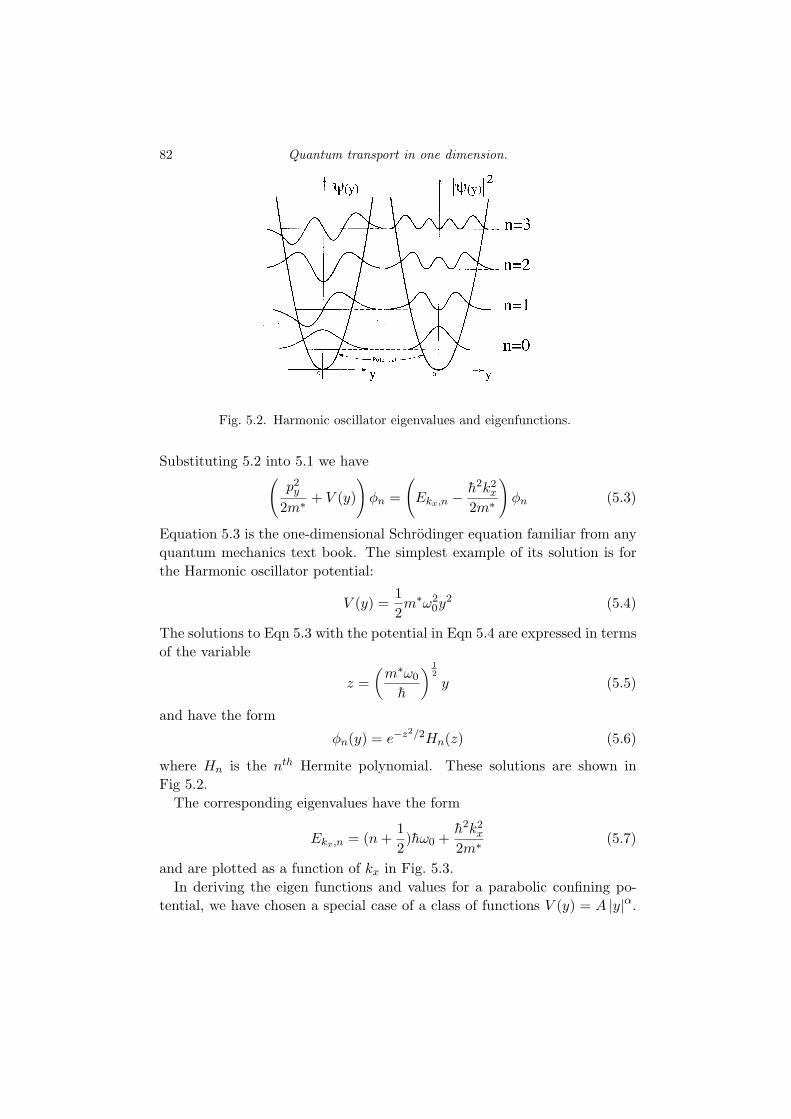
82 Quantum transport in one dimension.
Fig. 5.2. Harmonic oscillator eigenvalues and eigenfunctions.
Substituting 5.2 into 5.1 we have(
p2y
2m∗ + V (y)
)φn =
(Ekx,n − h2k2
x
2m∗
)φn (5.3)
Equation 5.3 is the one-dimensional Schrodinger equation familiar from anyquantum mechanics text book. The simplest example of its solution is forthe Harmonic oscillator potential:
V (y) =12m∗ω2
0y2 (5.4)
The solutions to Eqn 5.3 with the potential in Eqn 5.4 are expressed in termsof the variable
z =(
m∗ω0
h
) 12
y (5.5)
and have the form
φn(y) = e−z2/2Hn(z) (5.6)
where Hn is the nth Hermite polynomial. These solutions are shown inFig 5.2.
The corresponding eigenvalues have the form
Ekx,n = (n +12)hω0 +
h2k2x
2m∗ (5.7)
and are plotted as a function of kx in Fig. 5.3.In deriving the eigen functions and values for a parabolic confining po-
tential, we have chosen a special case of a class of functions V (y) = A |y|α.

5.5 Kardynal et al [2] 83
Fig. 5.3. Dispersion relation in a parabolic one-dimensional confining potential.
They have the property that for α > 2 the eigenvalues of increasing energybecome increasingly far apart in energy. The typical example is α → ∞,the square well. For α = 2 eigenvalues are equally spaced and for α < 2 thespacing between eigenvalues become smaller with increasing energy. Thetypical example is α = 1, the triangular well. For an arbitrary potentialV (y) the eigenvalues will have the form
Ekx,n = E0,n +h2k2
x
2m∗ (5.8)
We refer to the dispersion curve for each value of n as a one-dimensionalsubband and E0,n as the subband energy.
5.5 Kardynal et al [2]
Magnetotunnelling is an ideal probe of the quantum mechanical structurejust described. Fig. 5.4 shows an electronic device used to observe thesubband energies and wave functions of a quasi-one-dimensional electronsystem. The basic device consists of two parallel two-dimensional elec-tron systems (light grey) separated by a 125A AlGaAs barrier in a GaAs-AlGaAs heterostructure. Ohmic contacts (dark grey) contact the upperand lower two-dimensional systems independently so that current passedfrom the left contact to the right contact must pass through the upper two-dimensional system, tunnel across the barrier and pass out through the lowertwo-dimensional system. Independent contact to the two layers is achieved
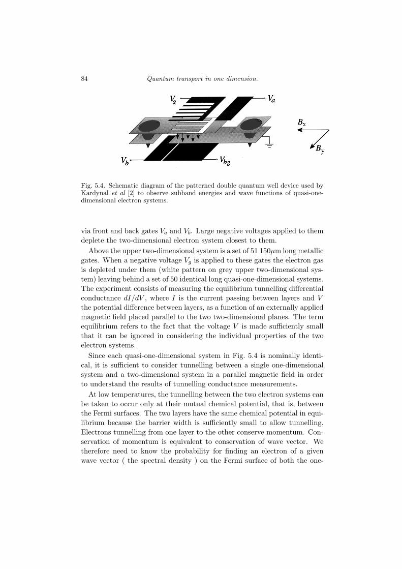
84 Quantum transport in one dimension.
Fig. 5.4. Schematic diagram of the patterned double quantum well device used byKardynal et al [2] to observe subband energies and wave functions of quasi-one-dimensional electron systems.
via front and back gates Va and Vb. Large negative voltages applied to themdeplete the two-dimensional electron system closest to them.
Above the upper two-dimensional system is a set of 51 150µm long metallicgates. When a negative voltage Vg is applied to these gates the electron gasis depleted under them (white pattern on grey upper two-dimensional sys-tem) leaving behind a set of 50 identical long quasi-one-dimensional systems.The experiment consists of measuring the equilibrium tunnelling differentialconductance dI/dV , where I is the current passing between layers and V
the potential difference between layers, as a function of an externally appliedmagnetic field placed parallel to the two two-dimensional planes. The termequilibrium refers to the fact that the voltage V is made sufficiently smallthat it can be ignored in considering the individual properties of the twoelectron systems.
Since each quasi-one-dimensional system in Fig. 5.4 is nominally identi-cal, it is sufficient to consider tunnelling between a single one-dimensionalsystem and a two-dimensional system in a parallel magnetic field in orderto understand the results of tunnelling conductance measurements.
At low temperatures, the tunnelling between the two electron systems canbe taken to occur only at their mutual chemical potential, that is, betweenthe Fermi surfaces. The two layers have the same chemical potential in equi-librium because the barrier width is sufficiently small to allow tunnelling.Electrons tunnelling from one layer to the other conserve momentum. Con-servation of momentum is equivalent to conservation of wave vector. Wetherefore need to know the probability for finding an electron of a givenwave vector ( the spectral density ) on the Fermi surface of both the one-

5.5 Kardynal et al [2] 85
k x
k y
0
Fig. 5.5. Spectral density of a two-dimensional electron gas at its Fermi energy -the Fermi circle.
dimensional and the two-dimensional system. The tunnelling conductanceof the device is then the overlap integral of these two spectral functions.
The wave functions in a two-dimensional system are plane waves
Ψkx,ky = eikxxeikyy (5.9)
and have a dispersion of the form
Ekx,ky =h2
2m∗(k2
x + k2y
)(5.10)
Hence, at the Fermi surface where Ekx,ky = EF there is only finite spectraldensity on a ring with k2
F = k2x + k2
y, where kF is the Fermi wave vector, asshown in Fig. 5.5.
The spectral density in a quasi-one-dimensional system is complicated(fortunately) by the fact that the wave function is only plane wave like inthe x - direction and composed of the non-plane wave like subband wavefunctions in the y - direction
Ψkx,n = exp(ikxx)φn(y) (5.11)
The dispersion relation for each subband n has the form
Ekx,n =h2k2
x
2m∗ + E0,n (5.12)

86 Quantum transport in one dimension.
so that, at the Fermi surface the values of kx are quantised (see Fig. 5.3)with
knx = ±
√2m∗(EF − E0,n)
h2 (5.13)
The two solutions in Eqn. 5.13 represent forward and reverse moving elec-trons. The spectral density for the nth subband at the chemical potentialhas the form
A1Dn (kx, ky) ∝ ∣∣FourierTransform
[Ψkn
x ,n(x, y; µ)]∣∣2
∝∣∣∣∣∫
dxdyeikxxeikyyΨknx ,n(x, y;µ)
∣∣∣∣2
∝∣∣∣∣∫
dxdy(eikn
xx + e−iknxx
)eikxxφn(y)eikyy
∣∣∣∣2
∝ (δ (knx − kx) + δ (−kn
x − kx))∣∣∣∣∫
dyφn(y)eikyy
∣∣∣∣2
(5.14)
The Fourier transforms of the subband wave functions that appear inequation Eqn. 5.14 are easily evaluated for the case of the Harmonic potentialsince ∫
dzeikze−z2/2Hn(z) ∝ e−k2/2Hn(k) (5.15)
For this special case the ky− dependence of the spectral density is exactlythe same as the y - dependence of the subband wave functions (these areshown in Fig. 5.2). In general, the two are not the same but the Fouriertransform of an arbitrary subband wave function always has exactly thesame number of maxima and minima as the wave function itself. Fig. 5.6is a schematic representation of the spectral function of a one-dimensionalsystem at its chemical potential with three occupied subbands.
The six vertical lines have kx values given by equation Eqn. 5.13 and aremodulated by the modulus squared of the Fourier transform of the respectivesubband wave functions as indicated by equation Eqn. 5.14. As we havesaid, the tunnelling conductance of the device in Fig. 5.4 is measured as afunction of an external magnetic field placed parallel to the two-dimensionallayers. The reason for this is that when an electron leaves the upper layerand tunnels to the lower layer in the presence of such an external field itspath is bent by the Lorentz force which alters the condition for conservationof momentum. Fig. 5.7(a) is a schematic diagram of the tunnelling processfor the case where the magnetic field is applied both parallel to the two-dimensional system and to the one-dimensional systems B = Bx.

5.5 Kardynal et al [2] 87
k x
k y
0
Fig. 5.6. Schematic diagram of the spectral density of a quasi-one-dimensional elec-tron gas with three occupied subbands.
d
Bx
d
By
ky ky - eBxd/h 1D 2D kx kx + eByd/h 1D 2D
(a) (b)
Fig. 5.7. (a) Effect on a tunnelling electron of a magnetic field in the x − direction(b) As for (a), for y - direction.
For this case momentum is conserved in tunnelling if
k2Dy → k1D
y +eBxd
h(5.16)
Equation 5.16 is justified in lecture notes 1 and strictly only applies to thecase where the one-dimensional and two-dimensional systems can be treatedas completely independent. The variable d is the distance between the cen-tres to the two quantum wells. Fig. 5.8(a) shows the spectral density for aone-dimensional system with six occupied subbands and the spectral den-sity for a two-dimensional system on the same graph. The one-dimensional

88 Quantum transport in one dimension.
k x
k y
kx
ky
Fig. 5.8. (a) Relative displacement of the spectral functions of the two-dimensionalsystem and the quasi-one-dimensional system for a magnetic field applied in the x- direction (b) for a magnetic field applied in the y - direction.
and the two-dimensional spectral densities are offset by ∆ky = eBxd/h in-dicating the overlap between equivalent k - states in the two systems atan arbitrarily chosen magnetic field Bx. The points where both spectraldensities have finite weight are the points in k - space where tunnelling oc-curs. The differential tunnelling conductance is given by the overlap of theone-dimensional and the two-dimensional spectral densities:
dI
dV∝
∫ ∫dkxdkyA2D
∑nOcc
A1Dn (5.17)
Fig. 5.7b is a schematic representation of the tunnelling process for thecase where the magnetic field is applied parallel to the two-dimensionalsystem and perpendicular to the one-dimensional systems B = By. For thiscase, momentum is conserved in tunnelling if
k2Dx → k1D
x − eByd
h(5.18)
Fig. 5.8(b) shows the equivalent of Fig.5.8(a) for this case.If we look again at Fig. 5.8(a) and ask how the overlap between the two-
dimensional and one-dimensional spectral densities varies as a function ofBx, we see that at zero magnetic field the two densities have no overlap andtherefore we expect zero dI/dV . As the magnetic field is increased the Fermicircle of the two-dimensional system passes across the spectral function ofthe one-dimensional system and a modulated dI/dV is observed. It is found

5.5 Kardynal et al [2] 89
Fig. 5.9. Magnetotunnelling differential conductance of the device shown in Fig. 5.4as a function of Bx taken at surface gate voltages Vg=-0.47,-0.48,...-0.62V - uppertrace to lower trace. The centre to centre distance between surface gates was 350nmand the gap between gates was 170nm.
that dI/dV is most strongly modulated by the spectral density variationsdue to the highest occupied subband with the contributions due to lowerenergy subbands tending to be smeared out giving an average background.Fig. 5.9 shows the tunnelling differential conductance of the device in Fig. 5.4at a series of different surfacegate voltages (Vg) for a magnetic field sweptin the Bx direction.
Each trace in Fig. 5.9 is an image of the highest occupied one-dimensionalsubband wave function in k - space. One can see how as Vg becomes increas-ingly negative the number of oscillations decreases and the symmetry of theoscillations varies from odd to even, indicating the sequence of subbanddepopulations.
If we now look again at Fig. 5.8(b) and ask how the overlap between Fermicircle and the one-dimensional spectral density varies as a function of By, wesee that as the magnetic field is increased, the tunnelling conductance is amaximum each time the trailing edge of the Fermi circle intersects with oneof the fixed kx values given by Eqn. 5.13. Fig. 5.10 shows the correspondingexperimental traces at a series of different gate voltages.
In Fig. 5.10 one can see how as Vg becomes increasingly negative, thenumber of oscillations decreases as subbands depopulate. From the kx peakpositions in Fig. 5.10, one can determine the subband energies using equationEqn. 5.13. These are shown in Fig. 5.11 as a function of surface gate voltage.

90 Quantum transport in one dimension.
Fig. 5.10. Tunnelling differential conductance of the device shown in Fig. 5.4 as afunction of By taken at surface gate voltages Vg=-0.48,-0.50,...-0.62V - upper traceto lower trace. The centre to centre distance between surface gates was 350nm andthe gap between gates was 170nm.
Fig. 5.11. Subband energies taken from Fig. 5.10 as a function of surface gatevoltage.
The subband energies in Fig. 5.11 show a tendency to become larger asVg is made more negative. This trend can be understood once the shapeof the effective potential V (y) as a function of the surface gate voltage isunderstood. Each of the traces in Figs. 5.9,5.10 are a cross-section of theone-dimensional spectral density at each gate voltage and the positions of

5.5 Kardynal et al [2] 91
Fig. 5.12. Experimental and calculated tunnelling differential conductance for Vg=-0.48V for Bx a,b and By c,d for the 350nm device a,c and the 570nm device b,d.(e) shows the best fitting potential profile for the 350nm device and (f) that for the570nm period device.
peaks in each trace are sufficiently unique that they can be used to determinethe shape of the effective potential (V (y) in Eqn. 5.1). Figures 5.12a,c showsingle tunnelling conductance traces (solid lines) for Bx and By for a devicewith ‘narrow’ quasi-one dimensional systems W ∼170nm.
Dotted lines in Figs.5.12a,c show the corresponding theoretical traces forthe effective potential shape, Fig. 5.12e, which gave the best match for peakpositions. In the narrow wire at the gate voltage shown, the electron densityis low and therefore cannot screen the external field from the surface gateswhich gives an effective potential of approximately parabolic shape and quitea strong curvature. Figures 5.12b,d,f show the equivalent to Figs. 5.12a,c,efor a ’wide’ quasi-one dimensional system W ∼ 230nm, measured at thesame gate voltage. In the wide wire the electron density is sufficiently highthat it can screen the external electric field from the surface gates to givethe effective potential a flat centre region.

92 Quantum transport in one dimension.
Fig. 5.13. (a) Device geometry. The layer thicknesses are 24nm for the undopedGaAs top layer, 36nm for the doped AlGaAs layer, 10nm for the undoped AlGaAsspacer layer and 6µm for the GaAs substrate. The donor binding energy and hetero-junction conduction band edge offset are taken to be 0.05 and 0.l2eV respectively.The calculation assumes a uniform surface charge density in the gate opening. (b)Calculated transverse potential profiles at 4.2K along a line 5.6nm from the GaAs-AlGaAs interface, near the mean of the vertical electron charge distribution for fourvalues of gate voltage.
Calculation of the shape of a quasi-one dimensional effective potentialis a complicated numerical task. It requires the simultaneous solution ofSchrodinger’s equation and the Poisson equation. Fig. 5.13a shows a deviceconfiguration for which a calculation was performed [3] and Fig. 5.13b showsthe resulting effective potential, V (y), at four different gate voltages. At -1.52V the potential is clearly well approximated by a parabola but at highergate voltages the screening by electrons gives it a flat centre region.
From the shape of these effective potentials we can understand the voltagedependence of the subband energies in Fig. 5.11. For the wide flat centredeffective potential found at low gate voltages the subband energies are closelyspaced and for the tight parabolic effective potential at high gate voltagesthe subband energies are large.
5.6 Density of States in a quasi-one-dimensional system
Each subband of a quasi-one-dimensional system defined by the Schrodingerequation 5.1 is an independent dynamically one-dimensional system. The

5.6 Density of States in a quasi-one-dimensional system 93
Fig. 5.14. Example of energy dependence of one-dimensional carrier density for asquare well confining potential.
density of states in a quasi-one-dimensional system is therefore a sum of thedensities of states for each one-dimensional subband.
If we consider a one-dimensional system of length L with periodic bound-ary conditions then kxL = 2πn, where n is an integer, so that the spacingbetween states in one-dimensional k-space is ∆kx = 2π/L. If the highestoccupied state has wave vector k, then the density of occupied states will be
n1 = (2k/∆kx) /L = k/π (5.19)
If we now substitute for k from Eqn. 5.13 the density in the nth subband forelectrons filled to energy E is for
nn =1
πh
√2m∗ (E − E0,n) for E0,n ≤ E
= 0 for E < E0,n (5.20)
so that the one-dimensional carrier density at zero temperature is
nc = g∑
n,E0,n≤E
1πh
√2m∗ (E − E0,n) (5.21)
g is the degeneracy of each one-dimensional subband g = 2 in GaAs andg = 4 in Si. Fig. 5.14 shows the carrier density of a square well potential asa function of energy evaluated using Eqn. 5.21.
If we now differentiate Eqn. 5.21 with respect to energy E the density of

94 Quantum transport in one dimension.
Fig. 5.15. One-dimensional density of states as a function of energy for a squarewell potential.
states has the form
ρ1D(E) = g∑
n,E0,n≤E
√2m∗
2πh(E −E0,n)−
12 (5.22)
Fig. 5.15 shows the density of states, evaluated using Eqn. 5.22, correspond-ing to Fig. 5.14.
5.7 Oscillation of the Fermi energy and Capacitance
The density of states modulation of a quasi-one-dimensional system is verysimilar to that of a two-dimensional system in a perpendicular magnetic fieldowing to the singularity at each subband energy. By comparison with thehigh magnetic field case, it is clear that this density of states modulation willcause oscillations in both the Fermi energy and the capacitance of a quasi-one-dimensional system. This section shows two experiments. The first is byLinda Macks and shows the oscillation of the Fermi energy through magneto-tunnelling measurements. The second is by Drexler and is a capacitancemeasurement of a set of induced quasi-one-dimensional systems.
5.7.1 Macks et al [4]
Figure. 5.16 shows the result of a magneto-tunnelling measurement on aset of 200 quasi-one-dimensional systems. The device structure was thesame as that shown in Fig. 5.4. The surface-gate array had a period of

5.7 Oscillation of the Fermi energy and Capacitance 95
(a) (b)
(c) (d)
Fig. 5.16. Magneto-tunnelling conductance of a set of parallel quasi-one-dimensional systems (a) By (b) Bx (c) Grey scale image of By. Arrows indicateevidence of pinning of one-dimensional subbands (d) Hartree calculation of theone-dimensional subband energies.
250nm and each gate had a width of 100nm and length 45µm. The quasi-one-dimensional systems were sufficiently narrow that by applying increas-ingly negative split-gate voltages the lowest five subbands could be observed:Figs. 5.16(a,b). A grey-scale image of the By dependence of the magneto-tunnelling conductance, Fig. 5.16(a), shows kinks in the trajectories of the1st and 2nd subband tunnelling peaks as the 3rd and 4th subbands pin atthe device chemical potential. Fig. 5.16(d) shows a selfconsistent Poissonand Schrodinger calculation of the 1D subband energies as a function ofsurface-gate voltage. It shows how the subband energies pin in regions ofhigh 1D density of states and jump in regions of low 1D density of states.It also shows the effect of this pinning on the effective potential minimum.At the most negative gate voltages it can be seen that the quantum wellactually deepens as the last subband depletes.

96 Quantum transport in one dimension.
(c)
Fig. 5.17. (a) Sketch of the interdigitated gate geometry of the top of the device andvoltage sources applied at the gate electrodes. (b) Cross-section of the sample. Theelectron systems are generated beneath the centre gate biased at voltage Vg. Theside gates are biased with respect to this gate by a voltage Vd. (c) The calculatedbare potential induced by the gate configuration in (b) at the location of the electronsystems with gate voltages indicated.
5.7.2 Drexler et al [5]
There have been a number of measurements of the oscillation of the capac-itance of a quasi-one-dimensional system but the clearest were performedby Drexler et al [5] using a GaAs-AlGaAs MISFET (Metal insulator semi-conductor field effect transistor). This device is similar to the Si MOSFETin that there is no electron gas at the heterojunction interface until a po-tential is applied to a surface gate. A set of parallel quasi-one-dimensionalsystems are induced by placing potential differences between two sets ofinterdigitated surface gates and a back gate - shown in Fig. 5.17.
The interdigitated surface gate geometry is formed by 300 metal stripsof 100nm width, 500nm period, and with 180µm length. The capacitancebetween the set of gates above the one-dimensional systems and a back gateis measured. Fig. 5.18 shows the measured capacitance.
Drexler et al assume that the backgate and the set of quasi-one-dimensionalsystems are at the same chemical potential. This gives the same series ca-pacitance relation as for the 2D case 1/C = 1/CG + 1/CQ. Where CG isthe geometric capacitance and CQ is the quantum capacitance which is pro-portional to the thermodynamic density of states. Thus in Fig. 5.18 thelarger the capacitance the larger the thermodynamic density of states. Thedifference between Fig. 5.15 and Fig. 5.18 - quite apart from Fig. 5.15 beingthe density of states and Fig. 5.18 being a measure of the thermodynamicdensity of states - indicates that for these wires, disorder and averaging over300 slightly different wires has nearly removed all modulation in the densityof states.

5.8 The Conductance of a quasi-one-dimensional system 97
Fig. 5.18. Capacitance of the wire array recorded as a function of the gate voltageVg. The values of n indicate the subbands that start to be filled in the correspondinggate voltage regimes.
5.8 The Conductance of a quasi-one-dimensional system
In a perfect quasi-one-dimensional system a current will travel in any one-dimensional subband without scattering into any other. If we consider cur-rent passing through a single subband labelled i between two perfect Ohmiccontacts. The left contact is at chemical potential µL = µ − eV and theright contact at chemical potential µR = µ where V is an applied potentialdifference between the two contacts. The current passing to the right in asmall energy range dε is then
dI+i = −evi
εf(ε + eV )12
dni
dεdε (5.23)
The term −eviε is the current in a single state in subband i at energy ε.
viε is the group velocity at energy ε in subband i defined by
viε =
1h
dEkx,i
dkx
∣∣∣∣ε
(5.24)
The second term f(ε + eV )12
dnidε dε is the number of electrons passing to
the right through subband i in the energy range dε around energy ε (note

98 Quantum transport in one dimension.
that the inclusion of the factor 1/2 is because the definition of ni in equationEqn. 5.19 includes electrons propagating in both directions but here we onlywish to include electrons passing to the right). Substituting Eqn. 5.19 andEqn. 5.24 into Eqn. 5.23 we find that the energy dependence of the groupvelocity and density of states cancel and we are left with
dI+i = − e
hf(ε + eV )dε (5.25)
That is, the current in any subband is independent of its index. A similarexpression is derived for states moving to the left in subband i
dI−i = − e
hf(ε)dε (5.26)
The total current flowing through subband i is then
Ii =∫ (
dI+i − dI−i
)=
e
h
∫ ∞
−∞(f(ε)− f(ε + eV )) dε (5.27)
In the limit of zero temperature this becomes
Ii =e2
hV (5.28)
If there are N subbands occupied in the quasi-one-dimensional systemthen the total current will be
I =∑
i
Ii = Ne2
hV (5.29)
which implies a conductance of
G = Ne2
h(5.30)
This result is quite remarkable, the conductance of a perfect quasi-one-dimensional system is equal to an integer multiple of e2/h. The experimentalconfirmation of this result [6,7] resolved a theoretical debate spanning thirtyyears [8].
5.9 Thomas et al [9]
Recent developments in growth and fabrication technology have producedquasi-one dimensional systems of astounding purity. It is interesting to quotefrom Thomas et al [9]:
“The samples used in this study were made from two modulation dopedGaAs-Al0.33Ga0.67As heterostructures, T119 and T166, grown by molecu-lar beam epitaxy. Both wafers have the same structure above the plane

5.9 Thomas et al [9] 99
of the two-dimensional system: 600A undoped Al0.33Ga0.67As spacer layer,2000A Si-doped (1.2x1017cm−3) Al0.33Ga0.67As layer, and 170A undopedGaAs cap layer. Split gates of width 0.75µm and length 0.4µm were de-fined on a Hall bar using electron beam lithography. Ohmic contacts weremade by thermal evaporation of Au/Ge/Ni alloys. After 20s of illumina-tion with a red light-emitting diode positioned 1cm away from the sample,the saturated values of the low temperature mobility and carrier concentra-tion of sample T119 were 3x106cm2/Vs and 1.9x1011cm−2, while those ofsample T166 were 1.5x106cm2/Vs and 1.9x1011cm−2. Prior to illuminationthe mobility and carrier concentrations were found to be less by 35% and50% respectively. Although both heterostructures have the same growthsequence, the electron mobility is higher in T119, as it was grown towardsthe end of a growth run. Two-terminal ac conductance measurements ofthe illuminated samples were carried out at the base temperature (less than100mK) of a dilution refrigerator using an excitation of 1µV at a frequencyof 85Hz. Curves (a) and (b) in Fig. 5.19 show the differential conductanceG(Vg) = dI/dVsd of two one dimensional constrictions in samples T166 andT119 respectively. Curve (a) shows 25 conductance plateaux and curve (b)shows 21 conductance plateaux quantised in units of 2e2/h, after subtrac-tion of a series resistance Rs which ensures that the lower plateaux alignwith the exact quantised values 2Ne2/h. Where N is the subband index.Upon application of a negative voltage Vg=-0.6V to the split gate, electronsare depleted from beneath both gates and the channel is defined; the con-ductance (see Fig.5.8 inset) drops dramatically at this definition voltage.As Vg is made more negative, the constriction is narrowed and the carrierdensity is reduced, and G decreases in units of 2e2/h as the one-dimensionalsubbands in the constriction are depopulated.”
The above passage mentions a series resistance that occurs in additionto the resistance of the split gate structure. The device is not a perfectmanifestation of a quasi-one-dimensional system connected to perfect Ohmiccontacts and therefore not all the voltage that is applied is dropped acrossthe device. The conductance is measured in units of 2e2/h because in zeromagnetic field GaAs has a spin degeneracy of 2.
Perhaps the most important observation for us to make in Fig. 5.19 isthat the conductance steps are not the perfect step functions predicted byEqn. 5.30 but have a finite spread to them that is much wider than thetemperature or excitation voltage used. One is tempted to say immediatelythat disorder broadens the steps and the result is therefore trivial. Howeverthe way in which disorder or any feature in the split gate effective potential

100 Quantum transport in one dimension.
Fig. 5.19. Differential conductance G(Vg) = dI/dVsd measured at a temperatureof T=50mK, quantised in units of 2e2/h after a series resistance RS has been sub-tracted: (a) sample T166 showing 25 quantised plateaux (RS=345Ω). (b) sampleT119 showing 21 quantised plateaux (RS=230Ω). Inset: raw data showing thedefinition and pinch off characteristics of: (1) sample T166 and (2) sample T119(data offset by 500µS).
broadens the ballistic steps is not at all trivial and requires a quantum-mechanical transport formalism to account for it.
5.10 The Landauer Formalism
If we wish to calculate the two-terminal conductance of a device such as thesplit gate device described above, there are two routes that are mathemati-
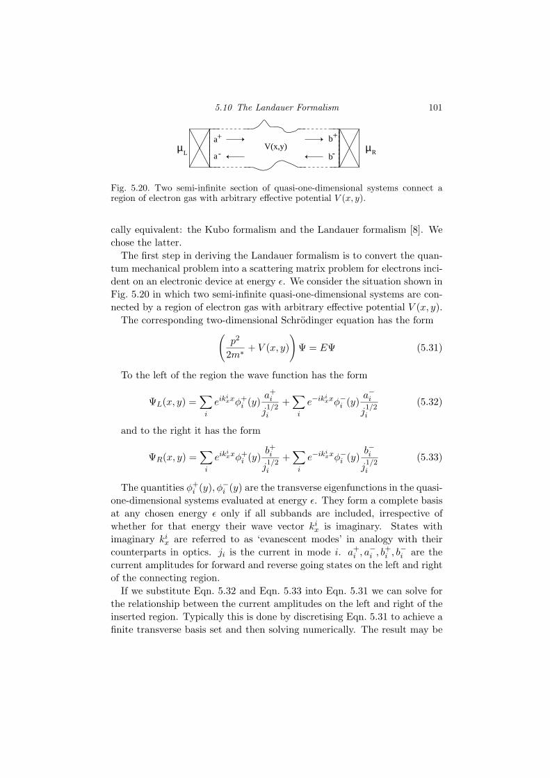
5.10 The Landauer Formalism 101
a+
a- b
b+
-V(x,y)µ µ
L R
Fig. 5.20. Two semi-infinite section of quasi-one-dimensional systems connect aregion of electron gas with arbitrary effective potential V (x, y).
cally equivalent: the Kubo formalism and the Landauer formalism [8]. Wechose the latter.
The first step in deriving the Landauer formalism is to convert the quan-tum mechanical problem into a scattering matrix problem for electrons inci-dent on an electronic device at energy ε. We consider the situation shown inFig. 5.20 in which two semi-infinite quasi-one-dimensional systems are con-nected by a region of electron gas with arbitrary effective potential V (x, y).
The corresponding two-dimensional Schrodinger equation has the form(
p2
2m∗ + V (x, y)
)Ψ = EΨ (5.31)
To the left of the region the wave function has the form
ΨL(x, y) =∑
i
eikixxφ+
i (y)a+
i
j1/2i
+∑
i
e−ikixxφ−i (y)
a−ij1/2i
(5.32)
and to the right it has the form
ΨR(x, y) =∑
i
eikixxφ+
i (y)b+i
j1/2i
+∑
i
e−ikixxφ−i (y)
b−ij1/2i
(5.33)
The quantities φ+i (y), φ−i (y) are the transverse eigenfunctions in the quasi-
one-dimensional systems evaluated at energy ε. They form a complete basisat any chosen energy ε only if all subbands are included, irrespective ofwhether for that energy their wave vector ki
x is imaginary. States withimaginary ki
x are referred to as ‘evanescent modes’ in analogy with theircounterparts in optics. ji is the current in mode i. a+
i , a−i , b+i , b−i are the
current amplitudes for forward and reverse going states on the left and rightof the connecting region.
If we substitute Eqn. 5.32 and Eqn. 5.33 into Eqn. 5.31 we can solve forthe relationship between the current amplitudes on the left and right of theinserted region. Typically this is done by discretising Eqn. 5.31 to achieve afinite transverse basis set and then solving numerically. The result may be

102 Quantum transport in one dimension.
written in matrix form as[
b+
a−
]=
[t+ r+
r− t−
] [a+
b−
]= S
[a+
b−
](5.34)
where a+, a−, b+, b− written now without subscripts are vectors containingthe amplitudes a+
i , a−i , b+i , b−i . The matrices t+, r+, t−, r− are the transmis-
sion and reflection matrices of the arbitrary region. The elements t+i,j , r+i,j , t
−i,j , r
−i,j
are the current transmission and reflection probability amplitudes. The ele-ments of the matrix S must be such that the current passing into the systemvia propagating modes is equal to the current passing out of the system viapropagating modes.
We now connect the quasi-one-dimensional leads to perfect Ohmic con-tacts with, as before, chemical potential µL = µ−eV on the left and chemicalpotential µR = µ on the right. On a microscopic level, the currents flowinginto each of the subbands of the quasi-one-dimensional systems from theOhmic contacts are random owing to the discreteness of electronic charge.In a simple transport measurement we detect the time averaged current.The average current flowing to the right in Fig. 5.20 in a small energy rangedε about energy ε is
dI+ =∑
i
〈∣∣∣b+
i
∣∣∣2〉time = 〈b+†b+〉time = 〈a+†t+†t+a+〉time
=∑
i,j
(t+†t+
)i,j〈a+∗
i a+j 〉time (5.35)
The time average 〈a+∗i a+
j 〉time simplifies because the amplitudes a+i , a+
j
for i 6= j for are uncorrelated in time so that
〈a+∗i a+
j 〉time = δi,j〈∣∣∣a+
i
∣∣∣2〉time (5.36)
The current entering each subband 〈∣∣∣a+
i
∣∣∣2〉time will be exactly the same
as was derived for the perfect case above
〈∣∣∣a+
i
∣∣∣2〉time = − e
hf(ε + eV )dε (5.37)
Unless it is an evanescent mode, for which the current will be zero. Sub-stituting Eqn. 5.37 and Eqn. 5.36 into Eqn. 5.35 we have
dI+ = − e
h
∑
iOcc
(t+†t+
)i,i
f(ε + eV )dε = − e
hTrace
[t+†t+
]f(ε + eV )dε
(5.38)

5.11 The saddle point potential 103
where the trace is over occupied states only. By a similar argument wederive
dI− = − e
hTrace
[t+†t+
]f(ε)dε (5.39)
Therefore the total current will be
I = − e
h
∫ ∞
−∞Trace
[t+†t+
](f(ε + eV )− f(ε)) dε (5.40)
The differential conductance G then has the form
G =dI
dV=
e2
h
∫Trace
[t+†t+
] (−df
dε
)dε (5.41)
In the limit of zero temperature this becomes
G =e2
hTrace
[t+†t+
](5.42)
where the expression is evaluated at the chemical potential.As we have derived them, Eqns. 5.41,5.42 give the conductance for an
arbitrary effective potential sandwiched between two semi-infinite quasi-one-dimensional systems attached to perfect Ohmic contacts. One mightreasonably ask what bearing this has on the experimental system describedabove. The answer is that in calculating the conductance of an electronicdevice using Eqns. 5.41,5.42 the connecting wires should be made as wideas possible and be joined smoothly to the arbitrary region so that any effectdue to their resistance or multiple scattering at the join is minimised.
5.11 The saddle point potential
We used the result of the calculation on the conductance of a perfect quasi-one-dimensional system to understand ballistic quantisation in an experi-mental split-gate device. However since the constrictions in these experi-ments are electrostatically induced by a pair of split gates, the potential isa smoothly varying function of position and therefore we must address thequestion of whether Eqn. 5.30 remains valid under these circumstances. Wefollow a paper by Buttiker [10] in describing this situation.
The bottle neck of a constriction forms a saddle point Fig. 5.21 which maybe expanded to second order as
V (x, y) = V0 − 12m∗ω2
xx2 +12m∗ω2
yy2 (5.43)

104 Quantum transport in one dimension.
yx
V(x,y)
Fig. 5.21. Schematic diagram of a saddle point potential.
Here V0 is the electrostatic potential in the middle of the saddle point,and the curvatures of the potential are expressed in terms of the harmonicoscillator energies Ex = hωx, Ey = hωy. The total energy is given by thepotential in equation 5.43 supplemented by the kinetic energy p2/2m∗. TheHamiltonian is separable into a transverse wave function associated withenergies (n + 1/2)Ey, n = 0,1,2,3... and a wave function for motion alongthe x - direction in an effective potential V0 + (n + 1/2)Ey − m∗ω2
xx2/2.This effective potential can be viewed as the band bottom of the nth one-dimensional subband in the region of the saddle point. In the absence ofquantum tunnelling the subbands with threshold energy
En = V0 + (n +12)Ey (5.44)
below the Fermi energy are open (fully transmitted) and the subbands withthreshold energy En above the Fermi energy are closed (perfectly reflected).Quantum mechanically transmission and reflection at the saddle allows forsubbands which are neither completely open nor completely closed, butwhich permit transmission with probability Tn,m = |tn,m|2. Here the in-dex n refers to the incident subband, and m refers to the outgoing subband.The transmission probabilities for this case are calculated in references [11]and can be expressed with the help of the variable
εn = 2[E −Ey
(n +
12
)− V0
]/Ex (5.45)

5.11 The saddle point potential 105
Fig. 5.22. Single subband transmission probabilities Tn,n and the total transmis-sion probability (conductance) T as a function of (E − V0)/Ex for the case whereEy/Ex = 3. The opening of successive one-dimensional subbands over narrowenergy intervals leads to the quantisation of the conductance.
in the simple form
Tn,m = δn,m1
1 + e−πεn(5.46)
Only transmission probabilities for which the incident subband and theoutgoing subband are the same are non-zero. Because of the quadraticform of the saddle-point there is no subband mixing. The transmissionprobabilities Tn,n for n = 0,1,2,3,4,.., for the case Ey/Ex = 3 are shown inFig. 5.22 as a function of (E − V0)/Ex.
For εn ¿ 0 the transmission probability is exponentially small: Tn,n →exp(−πεn) . For εn À 0 the transmission probability is close to one:Tn,n →1−exp(−πεn). The transition from zero transmission to a transmission prob-ability close to unity occurs in the neighbourhood of the classical thresholdenergy En in Eqn. 5.44. The size of the energy interval needed for the
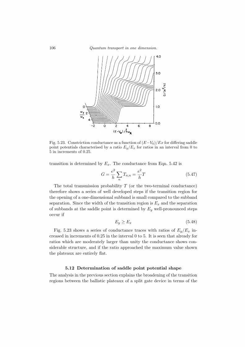
106 Quantum transport in one dimension.
Fig. 5.23. Constriction conductance as a function of (E−V0)/Ex for differing saddlepoint potentials characterised by a ratio Ey/Ex for ratios in an interval from 0 to5 in increments of 0.25.
transition is determined by Ex. The conductance from Eqn. 5.42 is
G =e2
h
∑n
Tn,n =e2
hT (5.47)
The total transmission probability T (or the two-terminal conductance)therefore shows a series of well developed steps if the transition region forthe opening of a one-dimensional subband is small compared to the subbandseparation. Since the width of the transition region is Ex and the separationof subbands at the saddle point is determined by Ey well-pronounced stepsoccur if
Ey ≥ Ex (5.48)
Fig. 5.23 shows a series of conductance traces with ratios of Ey/Ex in-creased in increments of 0.25 in the interval 0 to 5. It is seen that already forratios which are moderately larger than unity the conductance shows con-siderable structure, and if the ratio approached the maximum value shownthe plateaux are entirely flat.
5.12 Determination of saddle point potential shape
The analysis in the previous section explains the broadening of the transitionregions between the ballistic plateaux of a split gate device in terms of the

5.12 Determination of saddle point potential shape 107
EFEF
µ0
EF0
n=0
n=1
n=2
n=3
n=4
V(x)
x0
Fig. 5.24. (a)Split gate effective potential with no d.c bias applied. EF Fermienergy in leads. EF0 Fermi energy at the centre of the split gate.
ratio Ey/Ex and it is natural to ask how the curves in Fig. 5.23 can bematched with those in Fig. 5.19 to determine this ratio for an experimentaldevice. This is typically done by assuming that in an experimental split gatedevice V0 depends linearly on the gate voltage Vg and that both Ex and Ey
are constant over a small range of transitions. The ratio Ey/Ex is thereforefound by scaling the gate voltage axis of an experimental conductance tracelinearly until the plateau and transition widths can be matched with a tracefrom Fig. 5.23.
It is not possible to determine Ex, Ey individually from differential con-ductance traces such as those in Fig.5.19. However, if in addition to an a.cexcitation a d.c bias is applied across the device the Fermi surfaces on eachside of it can be used as probes of the subband energies. Fig. 5.24 shows across-section of the potential in a split gate device taken at the centre of theconstriction in the x - direction with no d.c bias applied.
The numbered lines drawn above the potential edge are the one-dimensionalsubband minima. The chemical potential is constant across the device andno current is flowing.
When a d.c bias is applied across the device capacitive coupling betweenthe electrons in the quasi-one-dimensional system and the surface gate willcause the electron density at each point in the device to change from itszero d.c bias/equilibrium value. However, this coupling is typically so smallthat even if a d.c bias of several milli volts were applied the density at anypoint would only be different from its equilibrium value by 0.1%. The ap-plication of the d.c bias therefore distorts the effective potential in such away as to keep the local density and therefore local Fermi energy constant( EF (x) ∝ n2D(x)). Fig.5.25 is a schematic representation of this where for

108 Quantum transport in one dimension.
EF
EF
EF0
n=0
n=1
n=2
n=3
n=4
V (x)
x0
µ = µ - eV/20L
µ = µ + eV/20R
Fig. 5.25. Distortion of split gate effective potential under the application of a d.c.bias. µL = µ0−eV/2 chemical potential on left hand side of device. µR = µ0+eV/2chemical potential on right hand side of device. µ0 equilibrium chemical potential,kept constant as an energy reference.
µ L
µ RΕ N+1
Ε Nµ L
µ RΕ N+1
Ε N
Ε N+2
Fig. 5.26. (a) Subband minima and left and right chemical potentials for the casewhere the applied d.c bias is smaller than the subband spacing. (b) case where thed.c. bias is larger than one subband spacing.
convenience we have chosen to make our energy reference point the equi-librium chemical potential µ0 so that for a potential difference V acrossthe device the chemical potential on the right is µR = µ0 + eV/2 and thechemical potential on the left is µL = µ0 − eV/2.
By using Fig. 5.25 as our model for the application of a d.c bias acrossa split gate device we may think of the subband energies in the centre ofthe saddle point as being unaffected by the application of the d.c bias butcapable of being moved up an down by the application of different split gatevoltages.
If, as in Fig.5.26a, both the left and right chemical potentials lie betweenthe subbands N and N +1 then at zero temperature we may write the totalcurrent as
I = I+ − I− = −Ne
hµL + N
e
hµR = N
e
h.2
eV
2= N
e2
hV (5.49)

5.12 Determination of saddle point potential shape 109
Fig. 5.27. Transconductance of a split gate device. The bottom trace correspondsto zero d.c bias and successive traces which are vertically off-set are different inapplied d.c bias by 0.08mV.
so that the differential conductance is
G =dI
dV= N
e2
h(5.50)
If, as in Fig. 5.26b, the left chemical potential lies between the subbandsN and N + 1 and the right chemical potential lies between the subbandsN + 1 and N + 2 then at zero temperature we may write the total currentas
I = I+ − I− = −Ne
hµL + (N + 1)
e
hµR = (N +
12)e2
hV +
e
hµ0 (5.51)
so that
G =dI
dV=
(N +
12
)e2
h(5.52)
In general we find that whenever a subband minimum at the centre ofthe saddle point passes either the left or the right chemical potential thedifferential conductance changes by an amount ∆G = e2/2h. This changein G implies a peak in the transconductance dG/dV g.
Fig. 5.27 shows a series of transconductance traces as a function of splitgate voltage for a split gate from reference [9].

110 Quantum transport in one dimension.
N
N-1
N+1
N+2
N+3/2N+3/2
N+1/2N+1/2
N-1/2N-1/2
V
Vg
0
Fig. 5.28. (a) Dark lines - transconductance of a split gate. Numbers - two terminalconductance. (b) Differential conductance within the saddle point model.
In Fig.5.27 at zero d.c bias as the split gate voltage is made more negativesuccessive subbands are depopulated at the centre of the saddle point. Eachtime this happens there is a peak in the transconductance. As the d.cbias increases each of these peaks slits into two. The peak at less negativegate voltage corresponds to the subband minimum passing across the leftchemical potential and the peak at more negative voltage corresponds tothe subband minimum passing across the right chemical potential. Thetrajectories of these peaks in the gate voltage Vg vs. d.c bias V plane arestraight lines: if we change the gate voltage and move a particular subbandminimum by an energy E then in order to keep it aligned with a particularchemical potential we must change that chemical potential by the sameenergy. Fig. 5.28a is a schematic diagram of the transconductance peaks ofa split gate device in the Vg vs V plane. Numbers indicate the value thedifferential conductance will have, in units of e2/h, in each diamond shapedregion defined by the peaks in the transconductance. Fig.5.28b shows thedifferential conductance calculated within the saddle point model at a seriesof different d.c. biases.
In Fig. 5.28a lines with positive gradients correspond to subband minimaaligning with the right chemical potential and lines with negative gradientcorrespond to subband minima aligning with the left chemical potential.
5.13 Exercises 111
Grey circles mark the points where transconductance peaks cross. Theyappear at set of gate voltages where at zero d.c bias two subband minimaare equally close to the chemical potential. The d.c bias at which theyoccur is equal to the spacing in energy between these two subbands. There-fore by accurately measuring the d.c bias at which these crossings occurthe corresponding subband spacings can be obtained. Other crossings oftransconductance peaks allow the determination of other subband spacings.However it is clear from Fig. 5.25 that the effective potential in the constric-tion becomes increasingly distorted by the d.c bias and therefore the energydifferences measured have no bearing on the zero d.c bias effective potential.
Fig. 5.28 has deliberately been drawn to indicate the experimental obser-vation that the measured subband spacings decrease with increasing gatevoltage. That is, if the constriction were a true parabolic saddle point po-tential then Ey would increase with increasingly negative gate voltage.
5.13 Exercises
5.1 A GaAs-AlGaAs heterostructure has a surface,a split-gate of width700nm and length 700nm patterned on its surface and a two-dimensionalelectron gas of density carrier density 1.0x10¹⁵m−2 250nm below itssurface.
(a) Calculate, assuming a simple capacitance model, the split-gatevoltage at which a one-dimensional channel would be defined by thesurface gates. Estimate the voltage at which the channel would pinchoff.
(b) Describe an experiment that would allow a determination ofthe dependence of the one-dimensional subband energies on split-gate voltage. Describe and account for the structure that would beseen.
(c) The two-terminal conductance of the first plateau has a valueG = 1.95e2/h. Assuming that a series resistance is responsible forthe deficit, what is the value of this resistance? Why would you ex-pect a series resistance?
(d) Why are the transition regions between conductance plateauxbroadened.

112 Quantum transport in one dimension.
(e) The curvature of the split-gate potential causes some inter-subband scattering. Will this necessarily destroy the ballistic quan-tisation?
(f) A d.c bias experiment is performed and it is found that peaksin the transconductance cross at the following points
n=1 , 2 :Vg= -5.0V Vdc= 2.5mVn=4 , 5 :Vg= -3.0V Vdc=1.0mVn=10 , 11: Vg= -1.0V Vdc= 0.5mV-amongst other points. Calculate the corresponding subband en-
ergies assuming that some of the applied d.c bias is dropped acrossthe series resistance ( use the series resistance calculated in (c) ). Ac-count for the trend you find in the subband energies with decreasinggate voltage. Approximately what would the width of the channel beat the chemical potential at the three gate voltages given assumingthat the potential is (i) parabolic (ii) square?
5.2 Why is there a singularity in the quasi-one-dimensional density ofstates. For finite size systems, is the one-dimensional density ofstates ever higher than the two-dimensional density of states. De-scribe the principle behind an experiments to observe the Fermi en-ergy modulation and the density of states modulation and accountfor the fact that singular behaviour is likely to be strongly damped.
Assume m∗ = 0.067me and ε = 13.0.
6
General quantum transport theory
6.1 Sources
[1] D. B. Chklovskii Phys. Rev. B 46 4026 (1992).[2] M. Bttiker Phys. Rev. B 41 7906 (1990).[3] B. J. van Wees et al Phys. Rev. B 38 3625 (1988).[4] B. E. Kardynal ph.D Thesis.[5] M. Bttiker Phys. Rev. B 38 9375 (1988).[6] L.P. Kouwenhoven, Masters Thesis, Delft University of Technology, 1988.[7] B. W. Alphenaar Phys. Rev. Lett. 64 677 (1990).
6.2 Introduction
This section of the notes extends the Landauer quantum transport theory tothe general case for finite perpendicular field with multiple Ohmic contacts.This will allow us to make a comprehensive study of the quantum Hall andShubnikov de Haas effects as measured on a standard Hall bar. The notescover: the quasi-one-dimensional system in finite perpendicular magneticfield, its eigen states, density of states, effective potential, and two-terminalconductance; the saddle point potential; the multi-probe Landauer-Buttikerformalism; edge states, disorder and the quantum Hall and Shubnokov deHaas effects.
6.3 Eigenstates of an infinite quasi-one-dimensional system
Schrodingers equation for a quasi-one-dimensional electron system with atransverse confining potential V (y) in a perpendicular magnetic field B =Bz has the form:
(1
2m∗ (p + eA)2 + V (y))
Ψ = EΨ (6.1)
113

114 General quantum transport theory
Although the physical system is translationally invariant in the x−directionEqn. 6.1 is only translationally invariant in the x−direction if we make asuitable gauge choice for A. Here we use the so called Landau gauge:
A = −Byx (6.2)
Substituting Eqn. 6.2 into Eqn. 6.1 and expanding the dot product wehave (
p2y
2m∗ +1
2m∗ (px − eBy)2 + V (y)
)Ψ = EΨ (6.3)
The translational invariance of the system implies that the solutions toEqn. 6.3 have the form
Ψkx,n = exp (ikxx)φkx,n (y) (6.4)
Substituting Eqn. 6.4 into Eqn. 6.3 we find(
p2y
2m∗ +12m∗ωc
(y − hkx
eB
)2
+ V (y)
)φkx,n = Ekx,nφkx,n (6.5)
Hence, in this gauge, the effect of the magnetic field is simply to add aparabolic potential
VB(y) =12m∗ω2
c (y − y0)2 (6.6)
where
y0 =hkx
eB(6.7)
to the effective potential V (y). This parabolic potential represents the effectof the Lorentz force. y0 is the classical centre of motion for electrons passingalong the quasi-one-dimensional system. It is referred to as the guidingcentre.
If we find the solutions to equation Eqn. 6.5 on the assumption that theeffective potential is parabolic
V (y) =12m∗ω2
0y2 (6.8)
they will give us sufficient insight to understand the nature of the solutionsfor an arbitrary confining potential. The sum of Eqn. 6.6 and Eqn. 6.8 inEqn. 6.5 results in an confining potential that is also parabolic. Equation 6.5can therefore be written in the form
(p2
y
2m∗ +12m∗ω2
c b2(
y − 1b2
y0
)2
+12m∗ω
20
b2y20
)φkx,n = Ekx,nφkx,n (6.9)

6.3 Eigenstates of an infinite quasi-one-dimensional system 115
y = y0y
E
V(y)
V (y)B
Fig. 6.1. Schematic diagram showing effective potential V (y) and magnetic effectivepotential VB(y) at an arbitrary position y = y0 together with the wave functionsand eigenenergies at this position.
where
b2 = 1 + ω20/ω2
c (6.10)
The solutions to Eqn. 6.9 are the same as those for Eqn.5.3 with confiningpotential Eqn.5.4 but with an origin offset by y0/b2
φy0,n(y) = e−(y−y0/b2)2/2l2BHn
((y − y0/b2
)/√
2lB)
(6.11)
where
lB =(
m∗ωcb
h
)− 12
(6.12)
The eigenvalues have the form
Ey0,n =(
n +12
)hωcb +
12m∗ω
20
b2y20 (6.13)
An example of the wave functions given by Eqn. 6.11with energies givenby Eqn. 6.13 is shown in Fig. 6.1 for a given value of y0. The wave functionsin Eqn. 6.11 are localised around classical cyclotron orbits that have radiiRn = lB
√2n + 1 and are centred on position y = y0. States that carry
momentum in opposite directions are forced close to opposite walls of thequasi-one-dimensional system even if they are at the same energy and havethe same Landau level index. The larger the momentum the further out fromthe centre y = 0 the states sit. If V (y) is a broad parabolic confinement

116 General quantum transport theory
Fig. 6.2. Subband energies of a 150nm wide square well as a function of magneticfield.
such that ωc À ω0 then b → 1 and Eqn. 6.13 takes the form
Ey0,n =(
n +12
)hωc + V (y0) (6.14)
This equation is the quasi-one-dimensional equivalent of Eqn.4.25. Sinceat high field lB is sufficiently small that at any position y0 an arbitraryeffective potential may be approximated locally by a parabola the high fieldeigenstates of an arbitrary effective potential will also be given by Eqn. 6.14.
Fig. 6.2 shows the subband energies E0,n of a quasi-one-dimensional sys-tem with a square-well effective potential V (y), of width W = 150nm, as afunction of magnetic field. It can be seen that all subband energies increasewith increasing magnetic field and that they fall onto the Landau levelsE0,n → (n + 1/2) hωc when their respective cyclotron orbits are smaller indiameter than the width of the system.
Figs. 6.3a,b,c,d are the dispersion curves for this system at four differentmagnetic fields. At zero magnetic field, Fig. 6.3a, the dispersion is parabolicand subband energies are proportional to the square of the subband index.

6.3 Eigenstates of an infinite quasi-one-dimensional system 117
(a) (b)
(c) (d)
Fig. 6.3. Dispersion curves for a 150nm wide square well at (a) 0.0T (b) 0.3T (c)1.0 T (d) 2.0T.
At B = 0.3, Fig. 6.3b, the effect of the magnetic field is noticeable in thespacing between the first and second subbands. At this field the cyclotronenergy is comparable to the zero field energy of the first subband. At B =1.0T the cyclotron diameters for the first two subbands are much smallerthan the width of the system. For guiding centre positions where the cy-clotron orbits do not intersect with the potential boundaries (y = ±75nm)the subband energies are dispersionless with energies equal to the cyclotronenergies. For guiding centre positions where the cyclotron orbit does in-tersect the potential boundaries the energies are no longer degenerate withthe cyclotron energies and rise in energy the more tightly they are pushedagainst the boundaries. Fig. 6.4a shows the wave function of the lowestsubband, in this system, for propagation in the positive direction, at anenergy of 10meV, for a series of different magnetic fields. Fig. 6.4b showsthe corresponding wave functions for propagation in the negative direction.

118 General quantum transport theory
Fig. 6.4. n=0 wave function at 10meV in a 150nm square well potential five mag-netic fields (a) negative momentum (b) positive momentum.
These two sequences show how the Lorentz force acts to push wave functionsagainst the walls of the system with increasing magnetic field.
6.4 Group Velocity
The group velocity of a state with wave vector kx in the nth Landau level isgiven by the gradient of the dispersion curve
vkx,n =1h
∂Ekx,n
∂kx(6.15)
If we consider Fig. 6.3d in light of this expression we see that states witha guiding centre position such that their cyclotron orbit does not touchthe walls of the wire have zero group velocity and are therefore stationarycyclotron orbits. Those states with orbits that touch the walls have a groupvelocity that increases the closer they are forced to the walls. This reflectsthe fact that electrons can only pass through the system by skipping alongthe edges of the wire these skipping orbits were discussed in notes 3. Thedensity of states therefore naturally splits into two parts: bulk states that

6.5 Density of states 119
are stationary cyclotron orbits and edge states that skip along the walls ofthe wire.
6.5 Density of states
The density of states in each subband is inversely proportional to the groupvelocity at any magnetic field. If we consider a finite wire with periodicboundary conditions we may write
dEn =∂En
∂kxdkx =
∂En
∂kx.πdn (6.16)
so thatdnn
dE=
22π ∂En
∂kx
=2
hvn(6.17)
Figs. 6.5a,b show the density of states of the quantum wire at zero mag-netic field and at one Tesla taken from Fig. 6.3a,c. They both have the samebasic shape but it can be seen that at high field, states are more localisedin energy around the subband energies.
Figure 6.6 shows data from the capacitance experiment by Drexler (notes5) performed at series of perpendicular magnetic fields between zero andseven Tesla. The traces at high field show the tendency towards greaterdegeneracy at subband energies. The experiment averages over 300 wireseach containing different disorder potentials. This averaging blurs the sharppeaks expected in the density of states.
6.6 Effective potential at high magnetic field [1]
Fig. 6.7a shows a smoothedged effective potential with occupied states markedby black dots of width lB. Fig. 6.7b shows the corresponding distributionof charge density from these occupied states. Where only the first Landaulevel is occupied the density is n(x) = eB/h and where the first and secondLandau levels are occupied the density is n(x) = 2eB/h. Fig. 6.7c shows astep-like effective potential edge and below it in Fig. 6.7d the correspond-ing density distribution. The two situations in Figs. 6.7a,b and Figs. 6.7c,dshow that owing to the nature of the eigenstates in a magnetic field a de-vice could have a smooth effective potential shape with a stepped densitydistribution or a stepped potential shape with a smooth density distribu-tion. The physical choice for an experimental system is the latter since thedensity distribution is determined by a smooth distribution of backgroundionised donors and remote surface gate potentials and is almost independent

120 General quantum transport theory
Fig. 6.5. Density of states in a 150nm square well potential (a) B=0.0T (b) B=1.0T.
of magnetic field. The discontinuities in the density distribution in Fig. 6.7darise from the fact that it is impossible to achieve the minimum energy den-sity distribution when lB is too small. The density distribution in Fig. 6.7dis therefore that which is closest to the minimum energy density distributiongiven the constraints that the eigenspectrum imposes.
6.7 Two-terminal conductance in a magnetic field
A quasi-one-dimensional system in a perpendicular magnetic field has twoimportant features in common with the zero field case. (1) Irrespective ofwhether a magnetic field is present or not the product of the group veloc-ity vn and the density of states nn for each one-dimensional subband is aconstant, independent of both energy and subband index
nnvn =1h
(6.18)
(2) Since all subband wave functions are eigenstates of the current opera-

6.7 Two-terminal conductance in a magnetic field 121
Fig. 6.6. Capacitance of the wire array recorded as a function of surface−gatevoltage Vg at different magnetic fields. The magnetic field increases in steps of 1Tfrom the top to the bottom trace. The scale refers to the top trace (B=0T) and aconstant offset is subtracted from the traces at finite magnetic field for clarity. Thevalues n = 1, 2, 3, 4 indicate the subbands that start to be filled in the correspondinggate voltage regimes.
tor a current passing into one subband will not scatter into other subbandsas it passes along the wire.
These two features make the steps we took to derive the two-terminalconductance of an infinite quasi-one-dimensional wire in zero magnetic field,Eqns.5.23−5.30, equally valid for finite magnetic field. In addition, and forthe same reason, the derivation of the generalised form for the two-terminalconductance, Eqns.5.31−5.42, is also valid at finite magnetic field. The onlydifference being that at zero magnetic field the transverse wave functionsare independent of both energy and direction of propagation. As we have

122 General quantum transport theory
Fig. 6.7. Effective potential at high magnetic field [1] (a) Smooth effective potentialshowing states below Fermi surface (b) Density distribution for (a). (c) Steppedeffective potential with states below Fermi surface (d) Density distribution for (c).
seen this is not the case for finite magnetic field since states propagating indifferent directions tend to be pushed towards opposite walls of the poten-tial. The two-terminal conductance of an arbitrary effective potential in amagnetic field and zero temperature may therefore be written
G =e2
hTrace
(t+†t+
)(6.19)
Whilst the form of Eqn. 6.19 is independent of magnetic field, the trans-mission coefficients are not. This is because they depend upon the functionalforms of the wave functions and eigenenergies.
6.8 The saddle point in a finite magnetic field [2]
We have shown that the effective potential in a quasi-one-dimensional systemchanges as a function of magnetic field − acquiring sharp steps in the highfield limit. However, if we consider a split-gate device at magnetic fieldsaway from this limit we can approximate its effective potential by a parabolic

6.8 The saddle point in a finite magnetic field [2] 123
x
y
Fig. 6.8. Saddle-point potential cut into sections.
saddle point - just as we did for the zero field case. In the Landau gauge,Schrodingers equation for the saddle point potential may be written
(p2
y
2m∗ +1
2m∗ (px − eBy)2 + V0 − 12m∗ω2
xx2 +12m∗ω2
yy2
)Ψ = EΨ (6.20)
Unlike the zero field case, this equation has no simple separation of vari-ables. However we can gain an idea of what its transmission and reflectioncoefficients will be like if we consider the potential as a series of narrowsections in which V (x) is constant −Fig. 6.8.
Schrodingers equation for the section centred on the point x has the form(
p2y
2m∗ +12m∗ω2
c
(y − hkx
eB
)2
+12m∗ω2
y
)φkx,n = E′φkx,n =
(E − V0 +
12m∗ω2
xx2)
φkx,n
(6.21)where we have made the substitution
Ψkx,n = exp(ikxx)φkx,n(y) (6.22)
Equation Eqn. 6.21 has the same form as equation Eqn. 6.9 and there-fore has wavefunctions of the form Eqn. 6.11 and eigenenergies of the formEqn. 6.13. These solutions consists of a set of independent subbands throughwhich current flows without scattering. If we now connect together two sec-tions and ask what happens at their boundary then it is clear that if theyjoin sufficiently smoothly the join will not cause any scattering betweensubbands. Thus if the whole saddle-point potential is sufficiently smooththere will be no scattering between subbands and the transmission matrixwill again be diagonal, as it was for the zero field case − Eqn.5.46. Thisis the case for the parabolic-saddle-point potential. Using the definition

124 General quantum transport theory
Fig. 6.9. Conductance of a saddle-point potential, with ωy/ωx = 1, as a functionof (E − V0)/Ex at a series of different magnetic fields ωc/ωx = 0, 0.25, ...5.
Ω2 = ω2c + ω2
y − ω2x the energies E1, E2 that govern transmission and reflec-
tion at a saddle-point potential in a magnetic field are
E1 =12
h√2
((Ω4 + 4ω2
xω2y
) 12 − Ω2
) 12
(6.23)
E2 =h√2
((Ω4 + 4ω2
xω2y
) 12 + Ω2
) 12
(6.24)
The transmission probability is a function of the variable
εn =E −E2 (n + 1/2)− V0
E1(6.25)
and is, as in the absence of a magnetic field, given by
Tn,m = δn,m1
1 + e−πε(6.26)
Fig. 6.9 shows the conductance of a saddle-point potential with ωy/ωx = 1at a series of magnetic fields. From the traces in this figure it is clear thatthe quantisation of the ballistic plateaux become increasingly accurate with

6.8 The saddle point in a finite magnetic field [2] 125
Fig. 6.10. Split-gate conductance (corrected for background resistance) as a func-tion of gate voltage for several magnetic field values, illustrating the transition fromzero-field quantisation to high field. The curves have been offset for clarity. Theinset shows the device geometry [3].
increasing magnetic field. The reason for this is that the magnetic fieldsuppresses backscattering by physically separating modes that propagate inopposite directions. Fig. 6.10 shows ballistic quantisation in a magnetic fieldtaken from experiment [3].

126 General quantum transport theory
6.9 Magnetic Depopulation [3,4]
The experimental traces in Fig. 6.10 and theoretical traces in Fig. 6.9 showa remarkable similarity that conceals an important difference between them.In the theoretical traces, at a particular value of the parameter (E−V0)/Ex,the number of transmitted subbands reduces with increasing magnetic fieldbecause the cyclotron energy increases and therefore at constant local Fermienergy EF0 = E−V0 in the centre of the constriction subbands must depopu-late. However, in the experiment at a fixed gate voltage it is the distributionof density that is constant and not the local Fermi energy. Subbands depop-ulate because the degeneracy of each Landau level increases with increasingmagnetic field. Figs. 6.11a,b give a detailed picture of how subbands depop-ulate in experiment [4].
It is interesting to note that the gate voltage at which the first subbandin a split-gate potential populates is independent of magnetic field. Thereason for this is that the gate voltage at which the first electrons arrive inthe device, and therefore the subband energy, is independent of magneticfield to within small corrections.
6.10 Multi-probe Landauer-Buttiker formalism [5]
Ballistic quantisation in a split-gate device and the quantum Hall effectare intimately related. However, ballistic quantisation derives from a two-terminal measurement, where the same Ohmic contacts are used to injectcurrent as are used to measure voltage, and the Hall effect derives froma four-probe measurement, in which current is passed between one pair ofOhmic contacts and voltage measured across another pair. The Shubnikovde Haas measurement is also a four-probe measurement. We have describedthese measurements in notes 4. In order to understand these measurementsbetter, we will derive a multi-probe version of the Landauer formula forconductance.
Fig. 6.12 shows a device structure with a number of Ohmic contacts. Ifwe consider the ith Ohmic contact then the total current Ii that this Ohmiccontact injects into the bulk of the device is made from three parts:
(1) Current injected directly:
Ii,injected = − e
hNiµi (6.27)
where Ni is the number of occupied propagating modes passing out fromOhmic contact i and µi is the chemical potential in lead i.

6.10 Multi-probe Landauer-Buttiker formalism [5] 127
Fig. 6.11. (a) Conductance of a split gate of lithographic width 450nm as a functionof split gate voltage measured at different magnetic fields. (b) A plot of the splitgate voltages at which subbands depopulate as a function of magnetic field. Linesare drawn as a guide to the eye. Note that the density in the wire was different in(a) and (b) and therefore they cannot be compared directly [4].
(2) Current which is reflected current back after passing into the bulk:
Ii,reflected =e
hRi,iµi (6.28)

128 General quantum transport theory
N1
N2
N i
Fig. 6.12. Multi-probe device.
The refection probability Ri,i has the form
Ri,i =Ni∑
ν1,ν2=0
∣∣∣ri,iν1,ν2
∣∣∣2
(6.29)
where ri,iν1,ν2
are the quantum-mechanical reflection amplitudes from sub-band ν2 in Ohmic contact i to subband ν1 in Ohmic contact i. They obeythe symmetry relation Ri,j(B) = Rj,i(−B) under reversal of the externalmagnetic field B.
(3) Current which is transmitted from other contacts:
Ii,transmitted = − e
h
∑
i6=j
Ti,jµj (6.30)
The transmission probabilities Ti,j have the form
Ti,j =Ni∑
ν1=1
Nj∑
ν2=1
∣∣∣ti,jν1,ν2
∣∣∣2
(6.31)
where ti,jν1,ν2are the quantum mechanical transmission amplitudes from
subband ν2 in Ohmic contact j to subband ν1 in Ohmic contact i. Theyobey the symmetry relation Ti,j(B) = Tj,i(−B) under reversal of the externalmagnetic field B.
The total current that Ohmic contact i injects into the bulk is then
Ii = Ii,injected − Ii,reflected − Ii,transmitted (6.32)
6.11 Edge states and obstacles 129
Ii = − e
h[Ni −Ri,i]µi − e
h
∑
i 6=j
Ti,jµj (6.33)
were Vi is the voltage on Ohmic contact i.
6.11 Edge states and obstacles
The problem with equation Eqn. 6.33 is that in order to find the outputpotentials µi and currents Ii for a given set of input potentials µ′i and cur-rents I ′i one must evaluate all of the reflection and transmission coefficientsfor the system. If done exactly, this is a task that must be done numericallyand can take hours of computational time. If one uses effective potentialscalculated selfconsistently, such as that shown in Fig. 6.7c, then the time forthis calculation must be added and it is easy to spend months calculatinga single magnetic field sweep or gate voltage sweep for comparison with aparticular experimental device. However, the existence of edge states sim-plifies the situation very considerably, offering a framework within whichmany high-field transport phenomena can be understood.
As we have seen, at high field, edge states can pass through a parabolicsaddle point potential without scattering. It is only when forward and re-verse travelling edge states are brought within a magnetic length of eachother that backscattering occurs and the transmission coefficient is reduced.Figs. 6.13b,c,d show three examples of edge states negotiating the randompotential shown in Fig. 6.13a. They are grey-scale representations of thewave function at the chemical potential. In Fig. 6.13b the two-terminal con-ductance was close to 3e2/h and one can make out the three bumps of thewave function passing from one Ohmic contact to the other. In Fig. 6.13c,dthe two-terminal conductances were close to 2e2/h and e2/h respectively.In general edge states behave like their classical counterparts - the skippingorbits. Edge states follow the equipotentials of an effective potential, how-ever contorted the path, and bound states form where the paths close onthemselves.
The picture of a random potential being carpeted by localised states thatwe used in notes 4 is now replaced by a picture in which complicated net-works of edge states follow every contour in the random potential at everyenergy. The puddles and peaks are still filled/covered with/by localisedstates but now they are bound edge states. At the percolation thresholdwhen the puddles link to form a continuous equipotential though the devicea single edge state is transmitted. This single state then remains at the

130 General quantum transport theory
Fig. 6.13. Grey-scale representations of (a) random effective potential in two-terminal device. (b) modulus squared of wave function at chemical potential whentwo-terminal conductance G = 3e2/h (c) G = 2e2/h (d) G = e2/h.
edge of the device as states are filled beyond the percolation point. WhenN Landau levels are filled there will be N edge states passing from one endof the Hall bar to the other in addition to the localised states. This situationis shown schematically in Fig. 6.14.
6.12 The Quantum Hall Effect
Fig. 6.15 shows a standard Hall bar, which we imagine to be very large incomparison to the magnetic length. We consider the situation where thechemical potential is in the localised states between Landau levels and N
edge channels pass into and out of each Ohmic contact. The Hall resistance isfound by passing a current I between Ohmic contact S and D and measuring

6.12 The Quantum Hall Effect 131
Bulk states
Edge States
Bulk States
Edge States
Fig. 6.14. (a) Cross-section of a Hall bar showing edge states and bulk states (b)Corresponding wave function at chemical potential c.f Fig. 6.13
S
A B
D
C
IN N N
NN
Fig. 6.15. Hall bar with N edge states passing between each Ohmic contact and acurrent I passing between S and D.
the voltage difference between Ohmic contacts A and C
Rx,y =VA − VC
I(6.34)

132 General quantum transport theory
N N
Fig. 6.16. Schematic of a single elastic scattering event at the edge of a Hall bar.
The corresponding diagonal resistance is found from
Rx,x =VA − VB
I(6.35)
Under these conditions equation Eqn. 6.33 gives five coupled linear equa-tions
I =e2
hNVS − e2
hNVC (6.36)
−I =e2
hNVD − e2
hNVB (6.37)
0 =e2
hNVA − e2
hNVS (6.38)
0 =e2
hNVB − e2
hNVA (6.39)
0 =e2
hNVC − e2
hNVD (6.40)
Equation 6.36 and Eqn. 6.37 describe current flowing out of S and intoD. Equations 6.38-6.40 describe voltage probes - for which no total currentflows in or out. We can immediately evaluate the diagonal resistivity inEqn. 6.35 since from Eqn. 6.39 VA = VB and therefore
Rx,x = 0 (6.41)
Using Eqn. 6.38 we find VA = VS substituting this into Eqn. 6.36 we find
I = Ne2
h(VA − VC) (6.42)
which gives
Rx,y =h
Ne2(6.43)
The experimental confirmation of the results in Eqn. 6.41 and Eqn. 6.43have been shown in Fig.4.3.
The quantum Hall effect derived in equations Eqns. 6.36-6.43 is extremelyrobust. Fig. 6.16 is a schematic representation of an elastic scattering event

6.12 The Quantum Hall Effect 133
S
A A A
D
A 1 2 n-1 n
B1 B2 Bn-1 Bn
Fig. 6.17. Hall bar with many Ohmic contacts along each edge. Note that interac-tion with an Ohmic contact can be thought of as an inelastic scattering event.
along the edge of a Hall bar. If all N edge states originate from the sameOhmic contact they will all be at the same potential. The scattering eventsimply redistributes current between states. The total current passing intothe event must equal the total current passing out and therefore equationsEqns. 6.36-6.40 remain valid in the presence of such scattering events and wewould measure the same Hall resistance Eqn. 6.43 and Shubnikov de Haaseffect Eqn. 6.41.
Fig. 6.17 shows a Hall bar with many Ohmic contacts along each edge.If a current is passed between S and D then equations Eqns. 6.33 take theform
I = Ne2
hVS −N
e2
hVB1 (6.44)
0 = Ne2
hVA1 −N
e2
hVS (6.45)
0 = Ne2
hVAi −N
e2
hVAi−1 (6.46)
−I = Ne2
hVD −N
e2
hVAn (6.47)
0 = Ne2
hVBn −N
e2
hVD (6.48)
0 = Ne2
hVBi −N
e2
hVBi+1 (6.49)
From Eqns. 6.48-6.49 we find VBi = VD and from Eqns. 6.45-6.46 we find

134 General quantum transport theory
1
2 3
4
56
Fig. 6.18. Reflection of edge states from a split-gate potential in a Hall bar. Medge states pass through the split gate and N edge states are occupied in the bulktwo-dimensional regions either side of the split gate.
VAi = VS therefore from Eqns. 6.44we have
I = Ne2
h(VAi − VBj ) (6.50)
so that
RSD,ij =h
Ne2(6.51)
which is independent of the contacts the voltage is measured between. Thuseven if edge states encounter phase-randomising events in Ohmic contactsor elsewhere the value of the quantum Hall effect is unaltered.
The theory of the quantum Hall effect predicts that there should be asmany edge states as there are occupied Landau levels. This prediction maybe tested directly by reflecting edge states from a split gate using the Hallbar configuration shown in Fig. 6.18.
The bulk two-dimensional system has N occupied Landau levels and thesplit gate reflects N −M edge states so that, at its centre only M Landaulevels are occupied. A current is passed between Ohmic contacts 1,4 andvoltages are measured between other contacts. Equations 6.33 give
I = Ne2
hV1 −N
e2
hV6 (6.52)
0 = Ne2
hV2 −N
e2
hV1 (6.53)
6.12 The Quantum Hall Effect 135
0 = Ne2
hV3 −M
e2
hV2 − (N −M)
e2
hV5 (6.54)
−I = Ne2
hV4 −N
e2
hV3 (6.55)
0 = Ne2
hV5 −N
e2
hV4 (6.56)
0 = Ne2
hV6 −M
e2
hV5 − (N −M)
e2
hV2 (6.57)
These equations are simplified, by noting that Eqns. 6.53 and 6.56 implythat V2 = V1 and V5 = V4, and by choosing Ohmic contact 1 to be at zeropotential. Thus we have
I = −Ne2
hV6 (6.58)
0 = Ne2
hV3 − (N −M)
e2
hV4 (6.59)
−I = Ne2
hV4 −N
e2
hV3 (6.60)
0 = Ne2
hV6 −M
e2
hV4 (6.61)
which give resistivities of the form
R14,26 =V2 − V6
I=
h
Ne2(6.62)
R14,25 =V2 − V 5
I=
h
Me2(6.63)
R14,23 =V2 − V3
I=
(1M
− 1N
)h
e2(6.64)
The Fractional quantisation predicted by Eqn. 6.64, that demonstrates thesuccessive reflection of edge states from a split gate, is readily observableexperimentally [6] Fig. 6.19.
The use of split-gates also allows the detection of inter-edge state scatter-ing directly. The Hall bar shown in Fig. 6.20 has a Hall resistance that issensitive to the current scattering probability S, between edge states origi-nating from Ohmic contacts 4 and 1, along the upper edge of the Hall bar.
A current I is passed between Ohmic contacts 1,3 and a voltage measuredbetween Ohmic contacts 2,4. Equations 6.33 have the form
I = Me2
hV1 −M
e2
hV4 (6.65)
0 = Me2
hV2 − (M − S)
e2
hV1 − S
e2
hV4 (6.66)

136 General quantum transport theory
Fig. 6.19. Fractional quantisation in the integer quantum Hall regime of the four-terminal longitudinal conductance R−1
14,23 of a split gate in a magnetic field of 1.4Tat T=0.6K. The solid horizontal lines indicate the quantised plateaux predicted byEqn. 6.64 with N=5 and M=1,2,3,4. The dashed lines give the location of thespin-split plateaux, which are not well resolved at this magnetic field [6].
1 2
34
Fig. 6.20. Hall bar used for the detection of inter-edge state scattering.
Rearranging Eqn. 6.66 we have
Me2
hV1 =
M2
M − S
e2
hV2 − MS
M − S
e2
hV4 (6.67)
so that
R13,24 =V2 − V4
I=
(M − S
M2
)h
e2(6.68)
Thus the Hall resistance is reduced by inter-edge-state scattering. Inhigh mobility two-dimensional systems such experiments have shown that

6.13 Exercises 137
electrons can travel in edge states without scattering for 1000µm or more[7].
6.13 Exercises
6.1 How does a perpendicular magnetic field affect the eigenstates ofquasi-one-dimensional system? What is the distinction between edgestates and bulk states? Why does the effective potential in a quan-tum wire acquire steps at high magnetic field?
6.2 Describe an experiment to determine the density of states modula-tion in a quasi-one-dimensional system at finite perpendicular mag-netic field.
6.3 What are Landau levels and how does their existence account for thequantum Hall effect in two-dimensional systems?
6.4 What is the nature of states in a Landau level in a disordered two-dimensional system? Why is disorder necessary to observe the quan-tum Hall effect?
6.5 Why is Landauers formula still valid in a magnetic field?6.6 Describe how a perpendicular magnetic field affects the shapes of
steps in the two-terminal conductance of a saddle point potential.6.7 How do edge states negotiate obstacles. Why is the quantum Hall
effect insensitive to scattering between edge states in a standard Hallbar geometry. Describe an experiment to detect scattering betweenedge states.

7
Quasi-particles in two dimensions
7.1 Sources
[1] R. P. Feynman R. B. Leighton and M. Sands, Lectures on Physics.[2] N. W. Ashcroft and N. D. Mermin, Solid State Physics.[3] D. Pines and P. Nozires, The Theory of Quantum Liquids.[4] R. D. Mattuck, A Guide to Feynman Diagrams in the Many-Body Prob-lem.[5] T. J. Gramila et al, Phys. Rev. B 47 12957 (1993).[6] J. P. Eisenstein, Superlattices and Microstructures 12 107 (1992).[7] N. P. R. Hill et al, J. Phys: Condens. Matter 8 L557 (1996).[8] J. K. Jain Adv. Phys. 41 105 (1992).[9] B. I. Halperin et al, Phys. Rev. B 47 7312 (1993).[10] N. Read Semicond. Sci. Technol. 9 1859 (1994).[11] R. Willett et al Phys. Rev. Lett. 59 1776 (1987).[12] R. R. Du. Phys. Rev. Lett. 75 3926 (1995).[13] V. J. Goldman et al Phys. Rev. Lett. 72 2065 (1994).[14] R. L. Willett et al, Phys. Rev. Lett 71 3846 (1993).[15] J. M. Shilton et al Phys. Rev. B 51 14770 (1995).[16] B. Rejaei and C. W. J. Beenakker, Phys. Rev. B 46 R15566 (1992).[17] A. S. Goldhaber and J. K. Jain Phys. Lett. A 199 267 (1995).[18] G. Kirczenow and B. L. Johnson, Phys. Rev. B 51 17579 (1995).[19] J. D. F. Franklin et al Surf. Sci. 361/362 17-21 (1996).
7.2 Introduction
In these notes we introduce the quasi-particle concept. This will give someinsight into why electron-electron interactions can frequently be ignoredwhen considering the transport properties of low-dimensional systems. Thetopics covered are: electrical forces; Landau’s theory of quasi-particles;
138

7.3 Electrical forces 139
quasi-particle decay; the temperature dependence of quasi-particle decay;the density-of-states dependence of quasi-particle decay; the formation ofnew quasi-particles under the influence of a quantizing magnetic field.
7.3 Electrical forces
Electrical forces are immensely strong. As pointed out by Feynman inhis lecture notes [1], if two people stand at arms length from each other,and each has one percent more electrons than protons, then the repellingforce between them is sufficient to lift a weight equal to that of the earth[1]! Electron-electron interactions in a two-dimensional electron systemcan also be very large. Consider a two-dimensional electron system in aGaAs/AlGaAs heterostructure with a carrier density of n2D=1.0x10⁻¹⁵m−2.On average electrons will be 320A apart so that the Coulomb force betweenadjacent pairs of electrons will be F = e2/4πεr2 = 2.0x10⁻¹⁴N. This is quitea small force from the perspective of a human but from the perspective ofan electron of effective mass m∗ = 0.067me it is a very large force. It issufficient to cause two electrons to accelerate away from each other at ap-proximately a billion-billion meters per second squared. In a GaAs-AlGaAsheterostructure it is the electrostatic attraction of the ionised donors thatprevents electrons from evacuating the system. In this case they provide aforce of attraction per electron that is an order of magnitude larger than therepulsion between electrons F = eE = e2n2D/ε= 2.2x10⁻¹³N. The ioniseddonors are therefore able to force the strongly interacting electrons togetherto maintain the two-dimensional system. In this system, given the strengthof the electron-electron interactions, one would expect the transport prop-erties to be dominated by inter-particle interaction effects. It is interestingto consider what the experiments on ballistic electron transport would yieldin this system or how the strong interaction might affect the observation ofballistic quantization or the quantum Hall effect. The answer to these ques-tions is simple yet quite surprising. Every experiment we have described todate has been performed in two-dimensional systems with densities similarto the case described above and yet we have been able to interpret each newphenomenon as if there is no interaction between electrons at all! The stronginteractions appear to change nothing. The reason for this was proposed byLandau in his theory of quasi-particles [2-3].

140 Quasi-particles in two dimensions
Interaction strength
Ener
gy
0
ε i
ε i+1
ε i+2
ε i-1
ε i-2
ε i-3
εi+2'
εi+1'
ε i'
ε i-1'
ε i-2'
ε i-3'
Fig. 7.1. Development of eigenstates of an electron system as the interaction be-tween electrons is slowly switched on.
7.4 Landau’s theory of quasi-particles [2-4]
Consider an electron system in which the interaction between electrons isswitched on very slowly such that every state of the non-interacting systemdevelops smoothly and adiabatically into a state of the interacting electronsystem Fig. 7.1.
If the interacting electron system is still in its ground state after thisprocess then it is referred to as a normal Fermi liquid. The two-dimensionalelectron system that forms at a heterojunction interface is an example of anormal Fermi liquid. There are many counter examples. Perhaps the bestknown are the superconductors in which the state achieved by adiabaticallyswitching on the interaction between particles is an excited state that canlose energy by forming Cooper-pairs.
The ground state of a normal Fermi liquid will have states filled accordingto Fermi-Dirac statistics and therefore will have a well defined Fermi surfaceat low temperature. The ground state is an equilibrium state with zeromomentum. If we consider an excited state of the non-interacting systemthat consists of the filled Fermi circle together with an additional particle ofmomentum p (Fig. 7.2a) then, due to conservation of momentum in particlecollisions, when the interaction is switched on we will generate an excitedstate of the interacting system also of momentum p (Fig. 7.2b).

7.4 Landau’s theory of quasi-particles [2-4] 141
p p
Fig. 7.2. Excited state of (a) a non-interacting system (b) an interacting system.The interacting system and the non-interacting system have exactly the same mo-mentum due to conservation of momentum in particle collisions.
Fig. 7.3. R. D. Mattucks horse (a) and quasi-horse (b) [4].
This additional particle slowly perturbs the distribution of other parti-cles in its vicinity as the interaction is increased. Once the interaction iscompletely switched on the additional particle will move around the systemsurrounded by the perturbation it produces. This particle, together with itsperturbation, is called a quasi-particle and may be considered to be an in-dependent entity that is a composite consisting of contributions from manyparticles. R. D. Mattuck in his consideration of quasi-particles [4] uses theidea of a horse galloping across a dusty plain to picture this concept. As thehorse moves along it kicks up a dust cloud that follows it producing therebya quasi-horse consisting of a horse and a dust cloud: Fig. 7.3a,b.
This analogy emphasizes the fact that the perturbation around the ad-ditional particle tends to screen the quasi-particles interaction with otherquasi-electrons just as the dust cloud tends to obscure the horse. Thisscreening happens because the perturbation tends to consist of the removal

142 Quasi-particles in two dimensions
Fig. 7.4. Newtons cradle.
of other particles from the additional particles vicinity leaving behind a pos-itive background of ionised donors. This positive background will partiallyneutralise the charge seen by other quasi-electrons.
The problem with the quasi-horse analogy is that it does not emphasizethe fact that electrons are indistinguishable. The cloud around the addi-tional electron is also made from electrons and it is not correct think of asingle bare electron entering the system creating a distortion in the particledistribution which then propagates together with the particle through thesystem. Within the quasi-horse analogy it would be better to think of ahorse running into a field of horses, causing a great deal of confusion, andsome time later another horse with the same momentum running out of thefield. An analogy that emphasizes this aspect of quasi-particle nature is theNewtons Cradle analogy. Newtons cradle consists of a row of metal ballshanging on strings Fig. 7.4.
The first ball is injected into the row with some momentum p a quasi-ballof momentum p then passes through the row of balls mediated by a stringof collisions and the final ball leaves the system with the same momentum.Depending upon the length of the row of balls several quasi-balls may beinjected at one time and quasi-balls travelling in opposite directions can bemade to collide and interact with each other.
Thus we have the answer to the question of why experiments see onlysingle-particle behaviour. Although an electron system at a heterojunctioninterface is composed of very strongly interacting electrons if we add a parti-cle with a particular momentum from a reservoir, as we do in transport mea-surements, conservation of momentum requires that a quasi-particle of thesame momentum propagate across the system. Quasi-particles are weaklyinteracting due to the screening that their particle perturbation provides.

7.5 Quasi-particles 143
7.5 Quasi-particles
The Hamiltonian for an interacting many-particle system can be written inthe form
H =N∑
i=1
((pi + eAi)
2m∗ + Vi(ri))
+N∑
i6=j=1
V (ri, rj) (7.1)
The first term represents a set of independent particles of mass m eachin their own effective potential Vi(ri). The second term represents interac-tions between these particles. As we have seen, the interaction term for thetwo-dimensional electron system, is typically very large. For the case weconsidered in the section on electrical forces the interaction was the sameorder of magnitude as the Fermi energy for each pair interaction. Thusthere is no sense in which we can think of the distribution of bare particlesas being perturbed by the interaction term for this case. It must absolutelydominate the solutions to Schrodinger’s equation. However, if we recall thetwo-body problem, a change of co-ordinates to a centre of mass co-ordinateand a relative co-ordinate reduces the interacting problem to two indepen-dent single particle problems. Most many-particle problems are reducible inexactly the same way, but through more general co-ordinate transformationsand gauge transformations:
Ri = Ri(r1, ..., rN , p1, ..., pN )
Pi = Pi(r1, ..., rN , p1, ..., pN )
A′i = Ai +∇φi (7.2)
These transformations are referred to as canonical transformations if thenew position and momentum co-ordinates obey the same commutation rela-tions as the original co-ordinates. Under these transformations the Hamil-tonian can be re-written in the form
H =N∑
i=1
((Pi + eαi)
2m∗ + Vi(Ri))
+N∑
i6=j=1
V (Ri, Rj , Pi, Pj) (7.3)
The first term represents a set of independent quasi-particles each withtheir own vector potential and electrostatic potential and the second termrepresents the interaction between these quasi-particles. If, as for the two-body problem, the transformation eliminates the interaction term then theHamiltonian describes a set of independent non-interacting quasi-particles.If the interaction term has been minimised by the transformation then wehave, in some sense, the best set of quasi-particles. As external conditions

144 Quasi-particles in two dimensions
εε
ε
ε
1
2
'
2'
µ
Fig. 7.5. Decay of a quasi-electron through the creation of a particle hole pair.
change, e.g magnetic and electric fields, what constitutes the best set ofquasi-particles will change.
7.6 Quasi-particle decay
As we have seen above, quasi-particles are only approximate eigenstates ofa real interacting system if the interaction term is not zero and therefore anexcited quasi-particle will decay through collisions with other quasi-particles.We can use this fact to probe the validity of Landaus Fermi liquid theory bymaking predictions about the temperature and density of states dependenceof the relaxation rate due to quasi-particle decay ( c.f notes 2).
Fig. 7.5 shows an example of a process in which a quasi-electron of energyε decays due to a collision with a quasi-electron of energy ε2.
The products of the decay are a quasi-electron of energy ε′1 and a quasi-electron quasi-hole pair with energies ε2 and ε′2. Higher order decay pro-cesses, in which several quasi-electron quasi-hole pairs are created, are possi-ble but occur at a much smaller rate. The relaxation rate for quasi-electronsof energy ε due to this type of particle decay may be written qualitativelyas
1τε∝
∫δ(ε+ε2−ε′1−ε′2)
ρ2(ε2)f0
2 dε2
ρ1(ε′1)(1− f01′)dε1′
ρ2(ε2′)(1− f0
2′)dε2′
(7.4)The delta function in Eqn. 7.4 is included to ensure conservation of energy
in the collision. Other conservation rules and the detailed nature of thequasi-particle collision are ignored since they do not affect the result weare trying to derive. ρ(ε) is the quasi-particle density of states and f0(ε)is the Fermi Dirac distribution function. The three terms in curly brackets

7.7 Resistivity 145
represent the availability of final states for the decay process.
ρ2(ε2)f02 dε2 = [average no. of quasi-electrons occupying dε2 around ε2]
ρ1(ε′1)(1− f01′)dε1′ = [average no. of quasi-holes occupying dε1 around ε1]
ρ2(ε2′)(1− f02′)dε2′ = [average no. of quasi-holes occupying dε2 around ε2]
(7.5)
The integral in Eqn. 7.4 has most of its weight within an energy range∆ε = ±max[ε, kBT ] of the chemical potential µ and therefore may be sim-plified if we consider a density of states that varies slowly over this energyrange. We may then write Eqn. 7.4 in the form
1τε∝ ρ3(µ)
∫δ(ε + ε2 − ε′1 − ε′2)f
02 (1− f0
1′)(1− f02′)dε2dε1′dε2′ (7.6)
Changing variables in Eqn. 7.6 to
xi =εi − µ
kBT(7.7)
we have
1τε
∝ ρ3(µ)(kBT )3
kbT
∫δ(x + x2 − x′1 − x′2)f
02 (1− f0
1′)(1− f02′)dx2dx1′dx2′
∝ ρ3(µ)(kBT )2(π2 + x2)(1− f0(x))
∝ ρ3(µ)(πkBT )2 + (ε− µ)2
1 + exp(
ε−µkBT
) (7.8)
The form of Eqn. 7.8 implies that at low temperature, quasi-particles withenergies close to the chemical potential will propagate through an interact-ing electron system over long distances without any collision affecting theirmotion. The fundamental reason for this is that at low temperature thereare no available states for the products of a decay process. At high temper-ature or at energies away from the chemical potential, quasi-particles willhave shorter life-times and the concept of a stable quasi-particle begins tobreak down.
7.7 Resistivity
The decay of quasi-particles gives rise to a resistivity that adds to that dueto impurity scattering and phonon scattering. We can derive its approxi-mate dependence on density of states and temperature using Eqn. 7.8. The

146 Quasi-particles in two dimensions
Ie
e
+ -
- +
VD
W
L
Drive
Layer
Drag
Layer
Fig. 7.6. Drag experiment. Drive and drag voltages have opposite sign.
resistivity is proportional to the average scattering rate
ρQPxx ∝ 〈 1
τε〉 =
∫ 1τε
(−∂f0
∂ε
)ρ(ε)dε
∝ ρ4(µ)(kBT )2∫ (x2 + π2) exp(x)
(1 + exp(x))3
∝ ρ4(µ)(kBT )2 (7.9)
This temperature dependence is difficult to observe experimentally in asingle two-dimensional system because at high temperature the resistivity isdominated by phonon scattering ρxx T 5 and at low temperature by impurityscattering ρxx const (c.f notes 2).
7.8 Temperature dependence of quasi-particle decay [5]
As we have said, the temperature dependence of quasi-particle decay is dif-ficult to see in a single two-dimensional system. However, Gramilla et al [5]have found a way to catch some of the quasi-electron quasi-hole pairs that arecreated when quasi-electrons decay by collision with other quasi-electrons.In their experiment a current I is passed through a two-dimensional electronsystem (the drive layer) that is in close proximity to, but electrically isolatedfrom, another two-dimensional electron system (the drive layer) as shown inFig. 7.6[6].
Quasi-electrons passing between Ohmic contacts in the drive layer occa-sionally ’collide’ with quasi-electrons in the drag layer thereby impartingmomentum to them. Many such events cause a build up of electrons at one

7.8 Temperature dependence of quasi-particle decay [5] 147
εε1'
µ
µε
ε2
2'
Drive
layer
Drag
Layer
1
2
Fig. 7.7. Decay of a drive layer quasi-electron through collision with a drag layerquasi-electron.
end of the drag layer and therefore a chemical potential difference betweendifferent ends. The voltage difference across the drag layer VD is of oppositesign to that in the drive layer. The drag resistivity is defined as the ratio ofthe drag electric field to the drive current density
ρD =VD/L
I/W(7.10)
By analogy with the Drude formalism we may write the drag resistivityin terms of a momentum relaxation rate
ρD =m∗
n1e2τD(7.11)
where τD is then the average time a quasi-electron propagates in the drivelayer before colliding with a quasi-electron in the drag layer. We may derivethe temperature and density of states dependence of the drag resistivityfollowing the analysis in Eqn. 7.4-7.10. Fig. 7.7 shows the ’collision’ processbetween quasi-electrons in the drive and drag layers.
This process has the same form as that shown in Fig. 7.5 except that twoof the final products of the decay process are in the drive layer and two inthe drag layer and therefore the drag resistivity will have the form
ρD ∝ 1τD
∝ ρ21(µ1)ρ2
2(µ2)T 2 (7.12)

148 Quasi-particles in two dimensions
Si - doped AlGaAs
AlGaAsbarrier
Si - doped AlGaAs
AlGaAsbarrier
GaAs well
AlGaAs barrier
GaAs well
700
200
175/225
200
700
(a) (b)
Fig. 7.8. (a) Wafer structure of bi-layer device (b) Conduction band edge.
where ρ1(µ1) and ρ2(µ2) are the densities of states at the chemical potentialsin the drive and drag layers respectively.
Fig. 7.8a shows the wafer structure used in [5] and Fig. 7.8b shows theconduction band edge for this wafer. Two parallel two-dimensional electronsystems form in the two quantum wells with nearly identical carrier densitiesn2D=1.5x10¹⁵m−2 and mobilities 350m2/Vs. The distance between the wellsis such that their wave functions are completely isolated from each other.The resistance of the barrier region between the wells was found to be 2MΩcompared to a sheet resistance of 10Ω/2. The wafer was patterned into aHall bar geometry using a mesa etch as shown Fig. 7.9.
If an Ohmic contact is required to contact only the top well then theback gate closest to that Ohmic contact is used to deplete the back two-dimensional electron system. If contact to the back two-dimensional systemis require the closest front gate is used. Fig. 7.10 shows the measured dragresistivity. It shows the expected T 2 dependence for the quasi-particle decayrate. This remarkable result confirms that at low temperatures even in astrongly interacting electron system quasi-particles interact only weakly. We

7.9 Density of states dependence of quasi-particle decay 149
Fig. 7.9. Hall bar used in drag experiment [6]. Each Ohmic contact, marked bycrosses, connects both two-dimensional electron systems to the surface of the mesa.Independent contact to each layer is achieved using a set of front and back gates(grey rectangles).
have therefore been justified in using single electron theory to predict thetransport properties of two-dimensional electron systems in notes 1-6.
7.9 Density of states dependence of quasi-particle decay
N. P. R. Hill et al [7] have performed a drag experiment using a bi-layerdevice similar to that of [5] but in the presence of a quantizing magneticfield. From equation Eqn. 7.12 the formation of an oscillating Landau leveldensity of states should lead to an oscillating drag resistivity in phase withthe single layer longitudinal resistivity. Fig. 7.11 shows the experimentalconfirmation of this result taken from [7].
7.10 Formation of new quasi-particles in a quantising magneticfield
We have shown that the quasi-particle scattering rate in a two-dimensionalelectron system increases as the fourth power of the density of states atthe chemical potential. The data from the N. P. R. Hill et al [7] is con-sistent with this prediction showing a strong increase in the quasi-particlescattering rate with increasing density of states. From our derivation of

150 Quasi-particles in two dimensions
Fig. 7.10. Drag resistivity as a function of temperature demonstrating the T 2 lawfor decay of quasi-particles [6].
quasi-particles it is clear that their form will change as the interactionstrength/type changes since in general a co-ordinate transformation thatworks for one strength/type of interaction will not work for another. Thischange is typically in the form of a change in effective mass but in a quan-tizing magnetic field a change in effective mass only affects the shape ofthe Landau levels and therefore cannot eliminate the interaction betweenquasi-particles. However, if at the peak of a Landau level ( half integerfilling factors ν = 1/2, 3/2, 5/2...) the interaction between quasi-particlesbecomes larger than the cyclotron energy it is clear that the system willhave sufficient energy to readjust itself in some way to screen this interac-tion. The way in which this is achieved is one of the most remarkable factsof nature.

7.11 Willett, Goldman and Du [8,11-12] 151
Fig. 7.11. Resistivity of bi-layer device of Hill et al [7] at temperature T=4.2K andmatched carrier densities n1=n2=2.3x10¹⁵m-2. (a) Diagonal resistivity of a singlelayer as a function of magnetic field (b) Drag resistivity between layers.
7.11 Willett, Goldman and Du [8,11-12]
Figs. 7.12-7.16 show the Shubnikov de Haas and Hall resistivities of four dif-ferent two-dimensional electron systems over different magnetic field ranges.Fig. 7.12 shows the result from the lowest mobility device. It has smoothShubnikov de Haas maxima and is a demonstration of ’text book’ integerShubnikov de Haas effect. Figs. 7.13-7.16 however show a great deal of addi-tional structure in their Shubnikov de Haas oscillations. The basic patternof the Shubnikov de Haas oscillations around zero magnetic field, shownin Fig. 7.12, appears to repeat itself around each half integer filling factor1/2, 3/2, 5/2, 7/2, ... and then again around each quarter integer fillingfactor 1/4, 3/4, 5/4, ... . If we interpret this structure as the Landau level
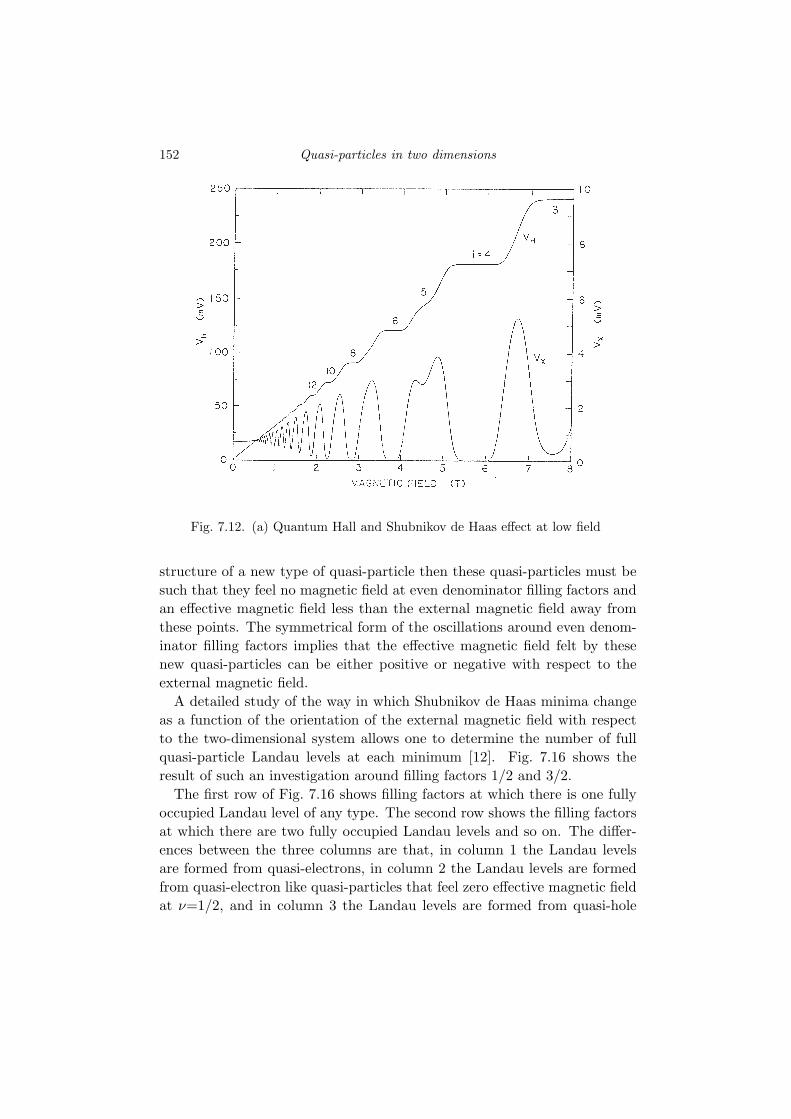
152 Quasi-particles in two dimensions
Fig. 7.12. (a) Quantum Hall and Shubnikov de Haas effect at low field
structure of a new type of quasi-particle then these quasi-particles must besuch that they feel no magnetic field at even denominator filling factors andan effective magnetic field less than the external magnetic field away fromthese points. The symmetrical form of the oscillations around even denom-inator filling factors implies that the effective magnetic field felt by thesenew quasi-particles can be either positive or negative with respect to theexternal magnetic field.
A detailed study of the way in which Shubnikov de Haas minima changeas a function of the orientation of the external magnetic field with respectto the two-dimensional system allows one to determine the number of fullquasi-particle Landau levels at each minimum [12]. Fig. 7.16 shows theresult of such an investigation around filling factors 1/2 and 3/2.
The first row of Fig. 7.16 shows filling factors at which there is one fullyoccupied Landau level of any type. The second row shows the filling factorsat which there are two fully occupied Landau levels and so on. The differ-ences between the three columns are that, in column 1 the Landau levelsare formed from quasi-electrons, in column 2 the Landau levels are formedfrom quasi-electron like quasi-particles that feel zero effective magnetic fieldat ν=1/2, and in column 3 the Landau levels are formed from quasi-hole
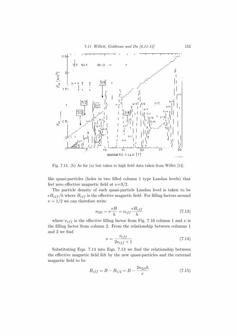
7.11 Willett, Goldman and Du [8,11-12] 153
Fig. 7.13. (b) As for (a) but taken to high field data taken from Willet [14].
like quasi-particles (holes in two filled column 1 type Landau levels) thatfeel zero effective magnetic field at ν=3/2.
The particle density of each quasi-particle Landau level is taken to beeBeff/h where Beff is the effective magnetic field. For filling factors aroundν = 1/2 we can therefore write
n2D = νeB
h= νeff
eBeff
h(7.13)
where νeff is the effective filling factor from Fig. 7.16 column 1 and ν isthe filling factor from column 2. From the relationship between columns 1and 2 we find
ν =νeff
2νeff + 1(7.14)
Substituting Eqn. 7.14 into Eqn. 7.13 we find the relationship betweenthe effective magnetic field felt by the new quasi-particles and the externalmagnetic field to be
Beff = B −B1/2 = B − 2n2Dh
e(7.15)

154 Quasi-particles in two dimensions
Fig. 7.14. (c) same as (b) but taken to higher field data taken from Goldmanpublished by Jain [8].
Around filling factor ν = 3/2 experiment suggests that quasi-particle Lan-dau levels with density eBeff/h are actually formed as Landau levels of holesin two filled non-composite fermion Landau levels, that is
n2D = νeB
h= 2
eB
h− νeff
eBeff
h(7.16)
Fig. 7.16 column 1 and ν is the filling factor from column 3. From therelationship between columns 1 and 3 we find
ν =3νeff + 22νeff + 1
(7.17)
Substituting Eqn. 7.17 into Eqn. 7.16 we find the relationship between the ef-fective magnetic field and the external magnetic field for these quasi-particlesto be
Beff = −3(B −B3/2) = −3B +2n2Dh
e(7.18)
Various tests for low field behaviour around ν = 1/2 have been performed

7.12 Composite fermions [16-17] 155
Fig. 7.15. (d) A detail around filling factor ν=3/2 data taken from Du [14].
[13-15]. Fig. 7.17 shows a comparison between a magnetic focusing experi-ment performed around zero magnetic field (c.f notes 3) and around ν = 1/2.One can see that they contain similar oscillatory structure demonstrating cy-clotron motion of composite fermions characteristic of the expected effectivemagnetic field Eqn. 7.15.
7.12 Composite fermions [16-17]
We have been discussing a new type of quasi-particle of a two-dimensionalsystem that feels an effective magnetic field rather than the actual external

156 Quasi-particles in two dimensions
Minima near
ν -> infinityWillet: minima near
ν=1/2
Du: minima near
ν=3/2
1
2
3
4
5
6
7
−1
−2
−3
−4
−5
−6
−7
∗
∗
1/3
2/5
3/7
4/9
5/11
6/13
∗
1
2/3
3/5
4/7
5/9
6/11
7/13
∗
∗
5/3
8/5
11/7
14/9
17/11
∗
∗
1
4/3
7/5
10/7
13/9
16/11
19/13
∗
∗
Fig. 7.16. Equivalent ρxx minima around B = 0, ν = 1/2 and ν = 3/2
magnetic field. To find such quasi-particles requires a gauge transformationof the two-dimensional many-particle Hamiltonian
H0 =1
2m∗∑
i
((pi + eA(ri))
2 + V (ri))
+∑
i<j
u(ri − rj) (7.19)
The relevant transformation for column 2 table 1 has the form
χφ =∏
i<j
(zi − zj)φ
|zi − zj |φ(7.20)
where zi = xi + iyi and (xi, yi) are the co-ordinates of the ith particle andφ is a real number. Under the transformation Schrodinger’s equation hasthe form
χ−1φ
H0χφΨ0 = Eχ−1φ
Ψ0 (7.21)
and the new Hamiltonian has the form
χ−1φ
H0χφ =1
2m∗∑
i
pi + eA(ri)− eφ
∑
j 6=i
a(ri − rj)
2
+ V (ri)
+
∑
i<j
u(ri−rj)
(7.22)

7.12 Composite fermions [16-17] 157
Fig. 7.17. Magnetic focusing experiment (c.f notes 3). (a) Data taken at ν = 1/2(b) Data taken at B=0. Taken from Goldman [13]. Composite fermions [16-17]
Eqn. 7.22 contains a gauge potential of the form
a(r) =h
2πe
z ∧ r
r2(7.23)
taking the curl of Eqn. 7.23 we find
∇∧ a =h
eδ(r)z (7.24)
The vector potential in Eqn. 7.23 therefore represents adding a tube ofmagnetic flux
Φ = −φh
e(7.25)
to the centre of an electron and the term eφ∑
i6=j a(ri − rj) in Eqn. 7.22represents adding such a flux tube to each electron in the system. The gauge

158 Quasi-particles in two dimensions
A
Fig. 7.18. Each composite fermion sees a forest of flux tubes from other compositefermions.
transformation Eqn. 7.21 has not changed the system in any way. The twoHamiltonians H0 and Hφ represent exactly the same physical system but interms of two different types of quasi-particle. The new quasi-particles withtheir attached flux are fermions if φ is an even integer and bosons if φ isan odd integer. This can be seen by calculating the Aharonov-Bohm fluxincurred in exchanging two of these quasi-particles. The new quasi-particlesare referred to respectively as composite fermions and composite bosons.The variety of interest to us here are the composite fermions.
7.13 Composite fermion effective magnetic field
A composite fermion propagating through a two-dimensional system maybe viewed as passing through a forest of flux tubes due to other compositefermions, Fig. 7.13, its dynamics being determined by the external vectorpotential plus the vector potential due to the flux tubes.
The vector potential the particle feels from the flux tubes fluctuates abouta mean background due to the constant motion of other composite fermions.This mean background is equivalent to a constant background magnetic fieldBg. If we consider some area A of a two-dimensional system containing N
composite fermions then the total flux enclosed will be
BgA = −φh
eN (7.26)

7.14 Composite fermion effective electric field 159
vd
B
E
vd
Beff
Eeff
(a) (b)
Fig. 7.19. (a) Drift velocity, external magnetic field and electric field for bare elec-trons in a wire (b) as for (a) but for composite fermions.
If the area taken is sufficiently large then
Bg = −φh
en2D (7.27)
where n2D is the carrier density of the two-dimensional system. Thisbackground magnetic field adds to the external magnetic field to give aneffective magnetic field felt by composite fermions
Beff = B − φh
en2D (7.28)
This is exactly equal to the effective magnetic field found experimentallyin Eqn. 7.15 if φ = 2. The same value of φ also gives the effective magneticfield in Eqn. 7.18 and the correct effective magnetic fields around all halfinteger filling factors. Taking φ = 4 in Eqn. 7.28 we find the correct effectivemagnetic fields around all quarter integer filling factors and so on.
The fractional quantum Hall effect may therefore be thought of as aninteger quantum Hall effect of composite fermions.
7.14 Composite fermion effective electric field
When a current passes along a wire in the presence of an external magneticfield B an electric field E builds up such that
0 = E + vd ∧B (7.29)
where vd is the drift velocity Fig.7.19a (c.f notes 2).The amplitude of the drift velocity is given by
vd = −E
B(7.30)
In the composite fermion gauge the quasi-particles respond to an effective

160 Quasi-particles in two dimensions
magnetic field Beff but, since the drift velocity is an average quantity, thatis independent of any gauge choice they must also respond to an effectiveelectric field Eeff such that
νd = −Eeff
Beff(7.31)
Combining equations Eqn. 7.30,7.31 and 7.15 the effective electric fieldfor the sequence of filling factors in column 2 of table 1 has the form
Eeff =Beff
BE = (1− φν)E (7.32)
This represents the production of a gauge electric field Eg of the form
Eg = −φνE (7.33)
which results from the motion of the composite fermion flux tubes andcan be determined directly by consideration of Faradays law.
7.15 Composite fermion Hamiltonian
We have established that if the fluctuations in the gauge magnetic field Bg
may be ignored then, in the composite fermions, we have a set of quasi-particles that behave in agreement with experiment. The single-particleHamiltonian for these composite fermions has the form
HS =1
2m∗ (p + eAeff )2 + V (7.34)
where
∇∧Aeff = Beff (7.35)
The potential term V includes the effective electric field.
7.16 Fractional quantum Hall effect
We found for the integer quantum Hall effect that when the chemical poten-tial was midway between two Landau levels the Hall effect took its classicalvalue. In the fractional quantum Hall regime the Hall effect takes its classi-cal value when the chemical potential is between composite fermion Landaulevels
ρxy =B
en2D=
h
νe2(7.36)
See Figs. 7.13-7.16.
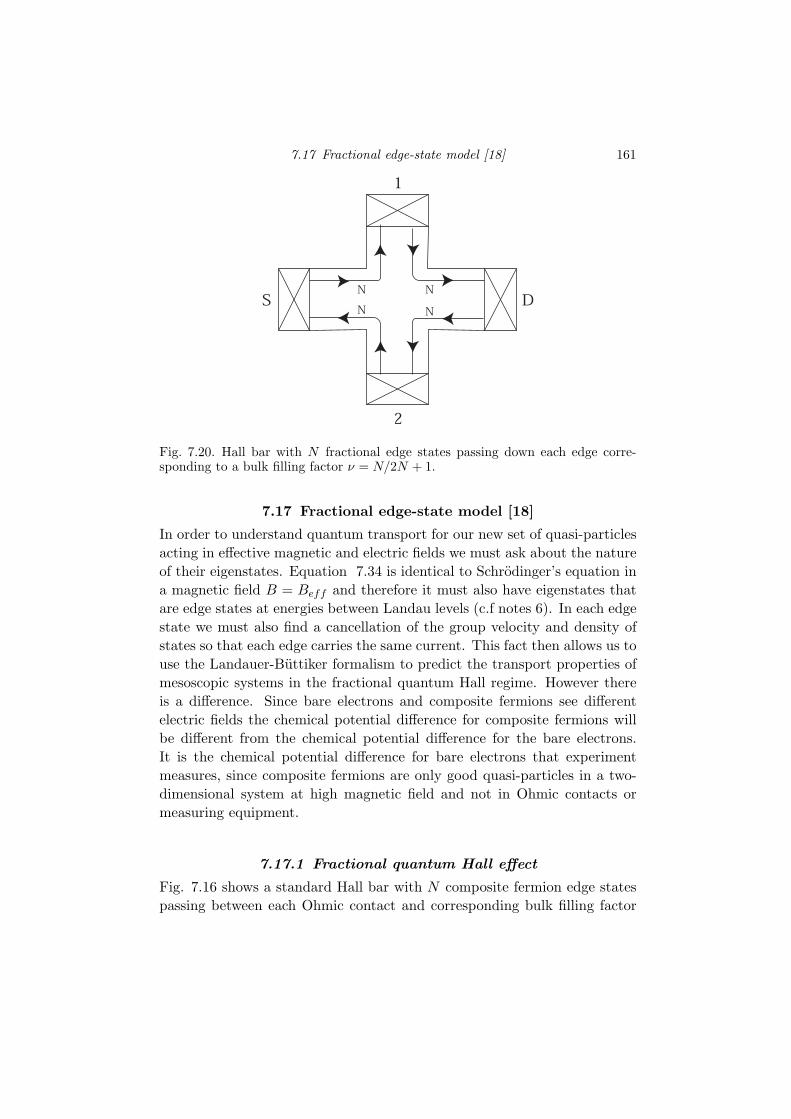
7.17 Fractional edge-state model [18] 161
S D
1
2
N N
N N
Fig. 7.20. Hall bar with N fractional edge states passing down each edge corre-sponding to a bulk filling factor ν = N/2N + 1.
7.17 Fractional edge-state model [18]
In order to understand quantum transport for our new set of quasi-particlesacting in effective magnetic and electric fields we must ask about the natureof their eigenstates. Equation 7.34 is identical to Schrodinger’s equation ina magnetic field B = Beff and therefore it must also have eigenstates thatare edge states at energies between Landau levels (c.f notes 6). In each edgestate we must also find a cancellation of the group velocity and density ofstates so that each edge carries the same current. This fact then allows us touse the Landauer-Buttiker formalism to predict the transport properties ofmesoscopic systems in the fractional quantum Hall regime. However thereis a difference. Since bare electrons and composite fermions see differentelectric fields the chemical potential difference for composite fermions willbe different from the chemical potential difference for the bare electrons.It is the chemical potential difference for bare electrons that experimentmeasures, since composite fermions are only good quasi-particles in a two-dimensional system at high magnetic field and not in Ohmic contacts ormeasuring equipment.
7.17.1 Fractional quantum Hall effect
Fig. 7.16 shows a standard Hall bar with N composite fermion edge statespassing between each Ohmic contact and corresponding bulk filling factor

162 Quasi-particles in two dimensions
ν = N/(2N +1). A current is passed between Ohmic contacts S and D anda voltage measured between Ohmic contacts 1 and 2. Using the Landauer-Buttiker formalism we find
I = Ne2
hV ∗
S −Ne2
hV ∗
2 (7.37)
0 = Ne2
hV ∗
1 −Ne2
hV ∗
S (7.38)
0 = Ne2
hV ∗
2 −Ne2
hV ∗
D (7.39)
−I = Ne2
hV ∗
D −Ne2
hV ∗
1 (7.40)
We have added stars to the potentials to indicate that they are the poten-tials that the composite fermions feel not those that are measured. Equa-tions 7.38 and 7.39 imply that V ∗
S = V ∗1 and V ∗
D = V ∗2 . Therefore from
equation 7.37 we find
I = Ne2
h(V ∗
1 − V ∗2 ) (7.41)
Since a current of magnetic flux is passing between ohmic contacts 1,2 wecan use Eqn. 7.32 to find the relationship between the composite fermionpotential difference and the bare electron potential difference measured inan experiment.
V ∗1 − V ∗
2 = EeffW = EW (1− 2ν) = (V1 − V2)(1− 2ν) (7.42)
where we have used φ = 2. Substituting Eqn. 7.42 into Eqn. 7.41 we find
I = N(1− 2ν)e2
h(V1 − V2)
=N
2N + 1e2
h(V1 − V2)
= νe2
h(V1 − V2) (7.43)
Hence
RSD,12 =h
νe2(7.44)
7.17.2 Reflection of composite fermion edge states
The fractional edge state model has withstood every experimental test thatthe integer edge state model has passed. A good example is the reflection

7.17 Fractional edge-state model [18] 163
1
23
4
56
Fig. 7.21. Selective reflection of edge states in the fractional quantum Hall regime.
of edge states from a split gate structure. Equations 6.58-6.61 from notes 6give
I = Ne2
h(V ∗
2 − V ∗6 ) (7.45)
I = Me2
h(V ∗
2 − V ∗5 ) (7.46)
I =(
1M
− 1N
)e2
h(V ∗
2 − V ∗3 ) (7.47)
Using Eqn. 7.32 we find
V ∗2 − V ∗
6 =(
1− 2N
2N + 1
)(V2 − V6) =
V2 − V6
2N + 1(7.48)
V ∗2 − V ∗
5 =(
1− 2M
2M + 1
)(V2 − V5) =
V2 − V5
2N + 1(7.49)
V ∗2 − V ∗
3 = V2 − V3 (7.50)
Therefore we have
R14,26 =V2 − V6
I=
2N + 1N
h
e2=
h
νbe2(7.51)

164 Quasi-particles in two dimensions
R14,25 =V2 − V5
I=
2M + 1M
h
e2=
h
νsge2(7.52)
R14,23 =V2 − V3
I=
(1M
− 1M
)h
e2=
(1
νsg− 1
νb
)h
e2(7.53)
where νsg and νb are respectively the filling factors in the split gate and inthe bulk. The results in Eqns.7.51-7.53 are what are observed experimentally- Fig. 7.21 [19].
7.18 Exercises
7.1 What is a quasi-particle and why is this concept necessary to accountfor single-particle explanations of mesoscopic phenomena?
7.2 What are the fractional quantum Hall and Shubnikov effects and howmay they be explained as an integer quantum Hall effect of compos-ite fermions? Why is disorder necessary to observe the fractionalquantum Hall effect?
7.3 Account for the temperature and energy dependence of the life timeof quasi-particles in a degenerate electron gas. Describe experimentsto probe each of these dependencies.
7.4 How can quasi-particles form in a quasi-one dimensional channel?Describe the passage of a quasi-particle across a saddle point poten-tial.
7.5 Account for the effective magnetic field which composite fermions re-spond to. Plot the effective magnetic field for the n=1/2 series com-posite fermions as a function of position across a parabolic channelat a series of characteristic densities at the channel centre.

8
Quantum dots
8.1 Sources
[1] L. P. Kouwenhoven et al Science p278 3 Dec (1997).[2] P. L. McEuen et al Phys. Rev. Lett 66 1926 (1991).[3] V. Fock Z. Phys. 47 446 (1928);C. G. Darwin Proc. Cambridge. Philos.Soc. 27 86 (1930).[4] U. Meirav and E. B. Foxman Semicond Sci Technol 10 p255 (1993).[5] Y. Aharonov and D. Bohm Phys. Rev. 115 485 (1959).[6] R. Webb et al Phys. Rev. Lett. 54 2696 (1985).[7] D. R. Mace et al Phys. Rev. B 52 R8672 (1995).
8.2 Introduction
In the first section of these notes we introduce the quantum dot - a quasi-zero-dimensional system confined in all three dimensions. We look at itsspectrum and conductance and discuss the role of the Coulomb interactionin determining the physics of both. In the second section we derive theAharonov-Bohm effect and look at its manifestation at low field and at high-field in edge-state networks. These notes cover: the experimental realizationof a quasi-zero-dimensional system; the single-particle eigen-spectrum ofa quasi-zero-dimensional system; single-particle conductance; experimentalconductance; classical Coulomb blockade; quantum Coulomb blockade; theartificial atom; the Aharonov-Bohm effect; and the Aharonov-Bohm effectwith edge states.
8.3 Quasi-zero dimensional systems [1,2]
Figure 8.1 shows two different types of quasi-zero-dimensional electron sys-tem, so called ‘quantum dots’, fabricated in semiconductor materials. The
165
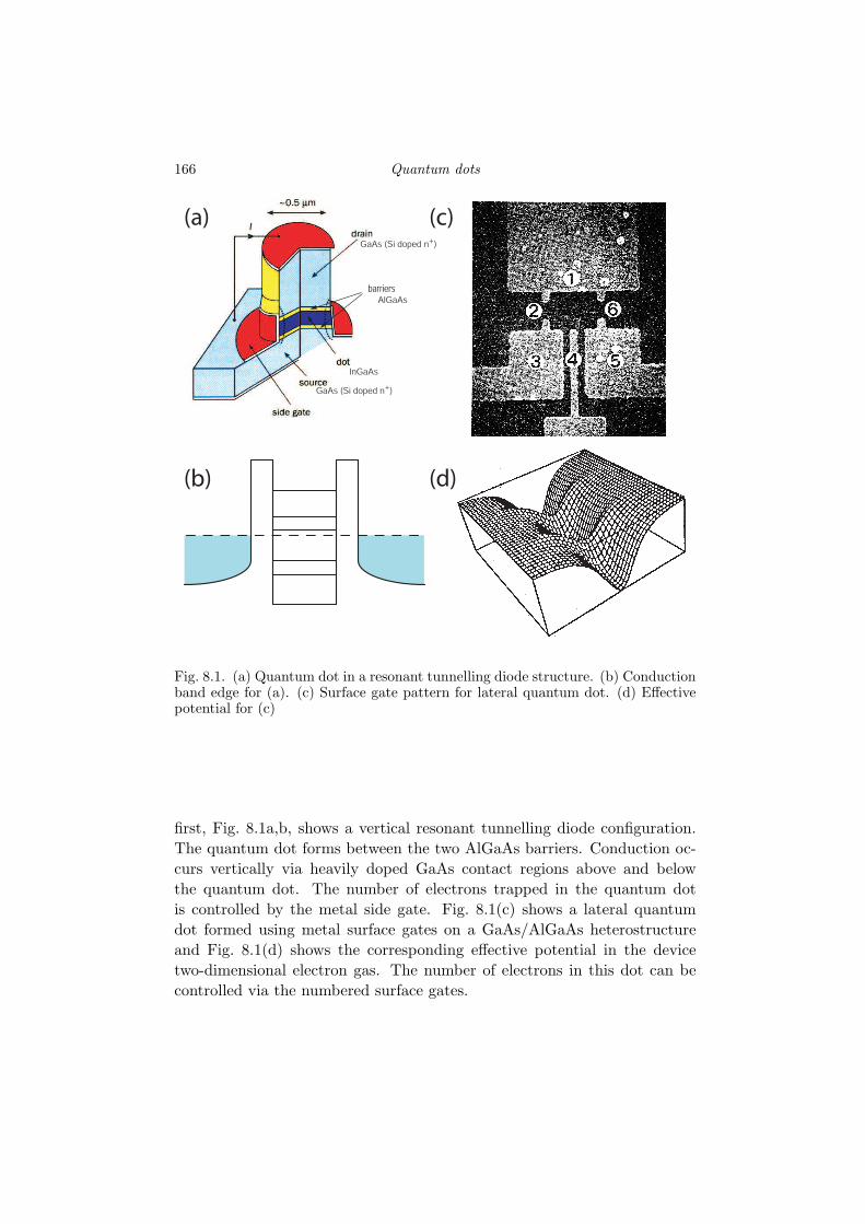
166 Quantum dots
GaAs (Si doped n+)
barrierAlGaAs
InGaAs
GaAs (Si doped n+)
barriers
(a)
(b)
(c)
(d)
Fig. 8.1. (a) Quantum dot in a resonant tunnelling diode structure. (b) Conductionband edge for (a). (c) Surface gate pattern for lateral quantum dot. (d) Effectivepotential for (c)
first, Fig. 8.1a,b, shows a vertical resonant tunnelling diode configuration.The quantum dot forms between the two AlGaAs barriers. Conduction oc-curs vertically via heavily doped GaAs contact regions above and belowthe quantum dot. The number of electrons trapped in the quantum dotis controlled by the metal side gate. Fig. 8.1(c) shows a lateral quantumdot formed using metal surface gates on a GaAs/AlGaAs heterostructureand Fig. 8.1(d) shows the corresponding effective potential in the devicetwo-dimensional electron gas. The number of electrons in this dot can becontrolled via the numbered surface gates.

8.4 The single-particle eigen-spectrum of a quantum dot [3] 167
8.4 The single-particle eigen-spectrum of a quantum dot [3]
Using Eqn. 4.15, Schrodinger’s equation,in the symmetric gauge A = (−By/2, Bx/2, 0),for a quantum dot with an effective potential V (r, φ) has the form
p2r
2m∗Ψ +ωC
2LZΨ +
12m∗ω
2C
4r2Ψ + V (r, φ)Ψ = EΨ (8.1)
Equation 8.1 can be solved exactly for a parabolic confining potential
V (r, φ) =12m∗ω2
0r2 (8.2)
The eigen-energies of this potential are
En,l = hωc
(b
(n +
12
)+
b |l| − l
2
)(8.3)
where
b =
√1 + 4
ω20
ω2C
(8.4)
Equation 8.3 has essentially the same form as Eqn. 4.20. The minus signthat appears in Eqn. 8.3 is a convention choice since, l, the azimuthal quan-tum number, may be either positive or negative. Fig. 8.2 is an evaluation ofEqn. 8.3 showing the generic form of the single-particle eigen-spectrum of aparabolic quantum dot.
8.4.1 Zero field limit
Equation 8.3 can be rearranged in the following way
En,l = hωcb
(n +
|l|2
)− hωcl
2(8.5)
Taking the zero field limit of ωcb
limB→0
ωcb = limB→0
√ω2
c + 4ω20 = 2ω0 (8.6)
equation Eqn. 8.5 then becomes
limB→0
En,l (8.7)
Equation 8.7 implies that at zero field the eigen-energies of a parabolicquantum dot are degenerate on integer multiples of hω0 since the term 2n+|l|+1 is an integer. The form of this term implies that an energy mhω0 willhave an m fold degeneracy.

168 Quantum dots
1 2 3 4 5 6 7
2
4
6
8
10
00
Magnetic Field (arb)
En
erg
y (h
ω0)
Fig. 8.2. Single-particle eigen-spectrum of a parabolic quantum dot.
8.4.2 High field limit
In the high field limit
limB→∞
b = 1 (8.8)
so that
limB→∞
En,l = hωc
(n +
12
+|l| − l
2
)(8.9)
For l ≥ 0
limB→∞
En,l = hωc
(n +
12
)(8.10)
For
limB→∞
En,l = hωc
(n + |l|+ 1
2
)(8.11)
All energies therefore converge on one or other Landau level at high field.
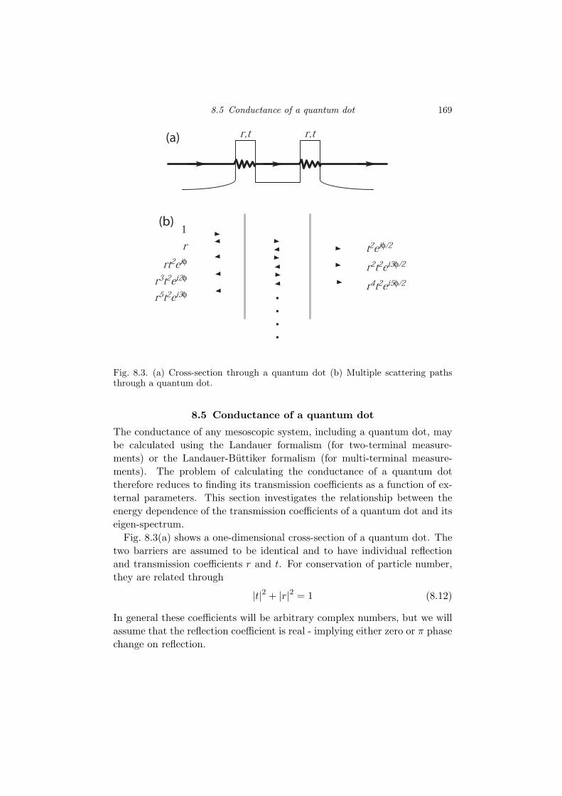
8.5 Conductance of a quantum dot 169
1
t2eiφ/2
r4t2ei5φ/2
r2t2ei3φ/2rt2eiφ
r3t2ei2φ
r5t2ei3φ
r
r,t r,t(a)
(b)
Fig. 8.3. (a) Cross-section through a quantum dot (b) Multiple scattering pathsthrough a quantum dot.
8.5 Conductance of a quantum dot
The conductance of any mesoscopic system, including a quantum dot, maybe calculated using the Landauer formalism (for two-terminal measure-ments) or the Landauer-Buttiker formalism (for multi-terminal measure-ments). The problem of calculating the conductance of a quantum dottherefore reduces to finding its transmission coefficients as a function of ex-ternal parameters. This section investigates the relationship between theenergy dependence of the transmission coefficients of a quantum dot and itseigen-spectrum.
Fig. 8.3(a) shows a one-dimensional cross-section of a quantum dot. Thetwo barriers are assumed to be identical and to have individual reflectionand transmission coefficients r and t. For conservation of particle number,they are related through
|t|2 + |r|2 = 1 (8.12)
In general these coefficients will be arbitrary complex numbers, but we willassume that the reflection coefficient is real - implying either zero or π phasechange on reflection.

170 Quantum dots
2 4 6 8 10
0.2
0.4
0.6
0.8
1.0
00.0
φ
|T|2
Fig. 8.4. (a)|T |2 for the quantum dot in Fig. 8.3(a) as a function of φ. (b)|T |2 as afunction of both φ and t.
When an electron enters a quantum dot it will scatter backwards and for-wards between the two barriers so that the total transmission and reflectioncoefficients are composed of a sum of all possible multiple scattering pathsthrough the dot. The contribution from each path is shown in Fig. 8.3(b).
From Fig. 8.3(b) the total transmission coefficient of the quantum dot inFig. 8.3(a) has the form
T = t2eiφ/2(
1 + eiφr2 +(eiφr2
)2+
(eiφr2
)3+ ...
)(8.13)
summing the series this gives
T =t2eiφ/2
1− eiφr2(8.14)
The two terminal conductance of the quantum dot then has the form
G =e2
h|T |2 =
e2
h
t2eiφ/2
1− eiφr2
t2e−iφ/2
1− e−iφr2=
e2
h
t4
1 + r2 − 2r2 cos(φ)(8.15)
Fig. 8.4(a) shows |T |2 as a function of φ for t = 0.5. The resonant peaks inthis figure are of unit height because the two barriers of the quantum dotare assumed to be identical. Fig. 8.4(b) shows |T |2 as a function of both φ
and t. In this figure it can be seen that for large values of t the transmissionresonances are broad and for small values of t they are narrow. On the leftside of this plot the transmission resonances are so narrow that they are notvisible within the resolution of the figure.
From Eqn. 8.15, it can be seen that the condition for a resonant peak inthe conductance is
φ = 2nπ (8.16)

8.6 McEuen et al [2] 171
where n is an integer. This establishes the link between the eigen-spectrumof a quantum dot and its transmission coefficient since Eqn. 8.16 is exactlythe condition for an eigenenergy of a quantum dot. Quantum dots there-fore transmit electrons resonantly when an eigenenergy passes the reservoirchemical potentials. Interference in multiple scattering strongly suppressestunnelling away from this condition.
8.6 McEuen et al [2]
Figure 8.5 shows the two-terminal conductance of the quantum dot in Fig. 8.1(b)as a function of the gate marked (1). Note that the vertical scale is loga-rithmic. The experiment shows temperature broadened resonant lines thatare similar in shape to those in Fig. 8.4(b). The fact that the peak heightsare an order of magnitude smaller between Figs. 8.4 and 8.6 could be ac-counted for by noting that there are many mechanisms that can reduce peakheight for example: temperature; asymmetry between barriers; and inelasticscattering.
8.6.1 Magnetic field dependence of resonant peaks [1,2]
At low densities the effective potential of a quantum dot will be approxi-mately parabolic, since screening is less efficient at low densities. We wouldtherefore predict that the resonant peaks shown in Fig. 8.5 should oscillatein magnetic field, and trace out the spectrum shown in Fig. 8.2, becauseof link we have established between the transmission resonances and theeigenstates of a quantum dot. Fig. 8.6a,b show the trajectories of resonantpeaks for both dots shown in Fig. 8.1. As can be seen, the resonant peaksin Fig. 8.6 oscillate as a function of magnetic field in a way that is similar tothe spectrum shown in Fig. 8.2. However, it appears as if the spectrum ofthe parabolic dot has been taken apart section by section in such a way thateach line in Fig. 8.2, which corresponds to a line of constant particle numberin the dot, is displaced in gate voltage from each other by a similar amount.This is demonstrated in the lower panel of Fig. 8.6(b) where these displace-ments have been removed. It shows (all be it in a wobbly way) a nice detailfrom the spectrum shown in Fig. 8.2. This offset between resonant peaksderives from the Coulomb interaction. The effect is known as ‘the Coulombblockade’ and is a mechanism which operates even in quantum dots that areso large that quantum mechanics is irrelevant.

172 Quantum dots
Fig. 8.5. Two-terminal conductance of the quantum dot shown in Fig. 8.1(b). De-tails show resonant line shapes.
8.7 Classical Coulomb blockade [4].
Consider a small metallic dot, Fig. 8.7, in weak electrical contact with tworeservoirs via two high resistance connections and capacitively coupled to anearby gate with a potential Vg applied to it. We imagine that the dot issufficiently large that its eigen-spectrum forms a continuum.

8.7 Classical Coulomb blockade [4]. 173
Fig. 8.6. (a) Trajectories of resonant peaks for Fig. 8.1(a). (b) for Fig. 8.1(b).
Vg
Cg
Fig. 8.7. Metal dot weakly coupled to reservoirs via tunnel barriers and capacitivelycoupled to metallic gate.
The electrostatic potential of electrons confined on the dot has the form
φ(Q) = Q/C + φext (8.17)
where Q is the charge on the dot, C is the capacitance between the dot andthe rest of the system, and φext is the external potential that arises from
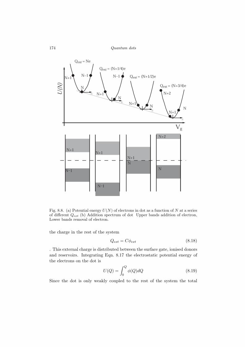
174 Quantum dots
N
Qext = (N+1/2)e
N+1
Qext = (N+1/4)e
NN+1
Vg
Qext = (N+3/4)e
NN+1
N+2
Qext = Ne
N
N+1N–1
U(N)
N–1
N
N–1
N+1N+1
N+1
N
N+2
N
N
N
N
N–1
Fig. 8.8. (a) Potential energy U(N) of electrons in dot as a function of N at a seriesof different Qext (b) Addition spectrum of dot Upper bands addition of electron,Lower bands removal of electron.
the charge in the rest of the system
Qext = Cφext (8.18)
. This external charge is distributed between the surface gate, ionised donorsand reservoirs. Integrating Eqn. 8.17 the electrostatic potential energy ofthe electrons on the dot is
U(Q) =∫ Q
0φ(Q)dQ (8.19)
Since the dot is only weakly coupled to the rest of the system the total

8.7 Classical Coulomb blockade [4]. 175
number of electrons on it must be an integer Q = Ne so that Eqn. 8.19becomes
U(N) =(Ne)2
2C−Neφext (8.20)
The external charge Qext may be varied continuously by means of the surfacegate Vg (in contrast to Q which is restricted to integer multiples of e).Rearranging Eqn. 8.20and substituting for φext, U(N) takes the parabolicform
U(N) = (Ne−Qext)2 /2C −Q2
ext/2C (8.21)
Fig. 8.8(a) shows U(N) from Eqn. 8.21 plotted for a series of different valuesof Qext as a function of N . The values of U(N) for which N is an integerare marked with black dots and labelled by the number of electrons trappedin the dot. For Qext = Ne it can be seen from Fig. 8.8(a) and Eqn. 8.17 andEqn. 8.21 that when the dot contains N electrons: the electrostatic potentialis zero φ(N) = 0; the electrostatic potential energy U(N) is a minimum; andthe minimum energy to add an extra electron is
U(N + 1)− U(N) =e2
2C(8.22)
Unless this energy can be supplied by the reservoirs (by putting a suf-ficiently large d.c. bias across the dot) electrons cannot hop onto the dotand its resistance will be very large. This phenomenon is referred as the‘Coulomb blockade’ because it is the Coulomb interaction that, under thesecircumstances, is preventing electrons from hopping onto the dot. The en-ergy difference U(N + 1) − U(N) is referred to as the minimum additionenergy. The addition spectrum of the dot is shown in Fig. 8.8(b) at thesame series of Qext used Fig. 8.8(a).
As Qext increases, with more positive Vg , it can be seen in Fig. 8.8(b)that the minimum addition energy decreases and becomes zero when:
Qext = (N + 1/2)e (8.23)
.At this point, it costs as much energy to have N electrons in the dot as
it does to have N + 1 and electrons may therefore hop onto or off the dotwithout experiencing any Coulomb blockade. The resistance of the dot isthen simply the sum of the resistances of the two contacts and the dot itself(this is its classical resistance value). A current will begin to flow throughthe dot once the d.c bias between reservoirs is larger than the minimumaddition energy.
176 Quantum dots
Once Qext increases past Qext = (N + 1/2)e there will be N + 1 electronstrapped in the dot and again it will be Coulomb blockaded since there willbe a gap to allowing the N + 2nd electron through. The sequence thenrepeats itself and the resistance is very large until Qext = (N + 1 + 1/2)e,where it is again equal to the classical resistance of the dot.
The conductance of a small metallic dot, as a function of an externalgate voltage, therefore consists of a series of equally spaced isolated peaksoccurring when there is no Coulomb blockade. The external potential φext
has a linear dependence on the surface-gate potential Vg so that for somechange in surface-gate voltage ∆Vg: ∆φext = α∆Vg. Between two peaks inconductance, one extra electron enters the dot and ∆Qext = e. Thereforethe spacing in gate voltage between conductance peaks is
∆Vg =e
αC=
e
Cg(8.24)
where Cg is the capacitance between the gate and the dot.
8.8 Quantum Coulomb blockade
Even though the Coulomb blockade is a classical effect, it is still importantin small quantum dots. In these systems, the potential energy U(N) is asum of the Coulomb charging energy Eqn. 8.21 and the energies of discretelevels in the dot
U(N) = (Ne−Qext)2/2C −Q2ext/2C +
N∑
i=1
εi (8.25)
Here εi represents the single-particle energy of the ith state measured relativeto the minimum of the quantum dot effective potential. It should be notedthat, as the dot fills, its effective potential changes and the nature of thesingle-particle spectrum changes. The minimum addition energy Emin ofa quantum dot containing N electrons then depends on the single-particleenergy for the N + 1st state
Emin = U(N + 1)− U(N) =(N + 1/2)e2 − eQext
C+ εN+1 (8.26)
In the classical case the addition energies above Emin form a continuum. Inthe quantum case they form a discrete set of energies Ei = Emin +εi−εN+1.Fig. 8.9 shows the addition spectrum at a series of different Qext. Once thed.c. bias between the reservoirs either side of a quantum dot is larger thanEmin electrons may tunnel through the dot. As the d.c. bias is increased

8.8 Quantum Coulomb blockade 177
EN+1
EN+2
EN+3
EN+1
EN+2
EN+3
EN+1
EN+2
EN+3
EN-2
EN-1
EN
EN-2
EN-1
EN
EN-2
EN-1
EN
EN-1
EN
EN+1
EN+2
EN+3
EN+4
Fig. 8.9. Development of addition spectrum of a quantum dot as Qext increases.
and successive single-particle states pass beneath the chemical potential ofeither reservoir the conductance increases in a series of steps.
At zero d.c. bias, a peak in the conductance of a quantum dot occurswhen its addition energy is zero. The resistance of a quantum dot will beless than the classical resistance because of resonant multiple scattering.Away from a resonant peak interference in multiple scattering may aid theCoulomb blockade and make it more resistive than the classical case.
From Eqn. 8.26 the external charge at a conductance peak is
Qext = (N + 1/2)e +C
eεN+1 (8.27)
so that, between the Nth and N + 1st peaks
∆Qext = e +C
e(εN+2 − εN+1) (8.28)
This implies that either slightly more or slightly less external charge, thanthe classical case, is required to compensate for differences in the single-particle energies as each extra electron is added to the quantum dot. Thespacings between peaks in gate voltage are then
∆Vg =e
Cg+
1αe
(εN+2 − εN+1) (8.29)
The single-particle energies therefore modulate the resonant peak positions

178 Quantum dots
Fig. 8.10. (a) Grey-scale plot of the transconductance of the quantum dot inFig. 8.1(a). Addition energies derived from the diamonds in (a).
confirming that the oscillatory structure in the spectra shown in Fig. 8.6does in fact derive from the single-particle spectrum of each quantum dot.
8.9 Artificial atoms
Figure 8.10(a) shows a grey-scale plot of the transconductance dG/dVg (Gis the differential conductance of the quantum dot dI/dVdc ) as a function ofdot gate voltage Vg and d.c bias Vdc for the quantum dot shown in Fig. 8.1(a).Just as for d.c bias measurements of a split-gate structures, see notes 6,each transconductance peak splits into two peaks in d.c. bias, one for eachchemical potential. The width of each diamond ( coloured black for clarityin Fig. 8.10(a)) gives the magnitude of the minimum addition energy foreach integer number of electrons filling the dot. These addition energiesare plotted in Fig. 8.10(b). The number next to each peak indicates thenumber of electrons occupying the quantum dot. Configurations with 2,6,12electrons have particularly high minimum addition energies. These fillingscorrespond to the zero field degeneracies of a parabolic quantum dot, oncespin is included, and they therefore correspond to complete two-dimensionalshells: nobel artificial atoms. This is shown schematically in Fig. 8.11.The other peaks correspond to half-filled shells indicating a two-dimensional

8.10 The Aharonov-Bohm effect [5] 179
Fig. 8.11. Shell structure of a two-dimensional artificial atom. Black and Greyrepresent the two spin species.
l0
l1
l2
l3
l4 l5l6
lN
dl
Fig. 8.12. Arbitrary line in a two-dimensional plane.
Hunds rule: in a partially filled shell the minimum energy configuration hasmaximum spin.
8.10 The Aharonov-Bohm effect [5]
The AharonovBohm effect is a truly quantum-mechanical phenomenon. Itis an interference effect that arises from the vector-potential dependence ofa wave function. The first step in understanding it is to find an expression

180 Quantum dots
for the way in which a wave function changes along an arbitrary path in amagnetic field.
In zero magnetic field Schrodinger’s equation, in a two-dimensional planewith an effective potential V (x, y), has the form
p2
2m∗Ψ + V (x, y)Ψ = EΨ (8.30)
If at a some point l in the plane, the wave function is Ψ(l) then some smalldistance dl away the it will be
Ψ(l + dl) = eip(l)
h.dlΨ(l) (8.31)
This assumes that the variation of the wave function is much faster than thevariation of the effective potential - allowing it to be treated locally as if itis constant. Iterating Eqn. 8.31 along the line in Fig. 8.12 we find
Ψ(lN ) = eip(lN )
h.dle
ip(lN−1)
h.dl...e
ip(l1)
h.dlΨ(l0) (8.32)
This can then be written as
Ψ(lN ) = ei∫ lN
l0
p(l)h
.dlΨ(l0) (8.33)
At finite magnetic field we must subtract the field momentum from thecanonical momentum to get the correct kinetic energy in Schrodinger’s equa-tion Eqn. 8.30. This gives the following replacement in Eqn. 8.33: p → p+eA
so that
Ψ(lN ) = ei∫ lN
l0
p(l)+eA(l)h
.dlΨ(l0) (8.34)
This equation shows that the phase accumulated in passing along an arbi-trary path in a two-dimensional plane depends both on the canonical mo-mentum p and the field momentum eA.
The Aharonov-Bohm effect is most strikingly seen in the situation shownin Fig. 8.13. It consists of a wire that constrains electrons to move in a circlearound a region that has a finite magnetic field B in an area S somewhereenclosed within it. From a classical perspective, we would not expect theelectrons to have any part of their motion affected by the enclosed magneticfield since they will not actually move through any region where the mag-netic field is finite. However, the particle’s wave function is affected by theexistence of the enclosed flux. From Eqn. 8.34 the total phase accumulatedin passing round the loop will be
∆φ =∮
p + eA
h.dl =
2πrp
h+
e
h
∫∇∧A.dS =
2πrp
h+
e
h
∫B.dS (8.35)

8.11 Webb et al [6] 181
B
Fig. 8.13. Electron moving in a circle around a region of finite magnetic field B ofarea S.
where r is the radius of the electron loop so that
∆φ =2πrp
h+ 2π
e
hBS (8.36)
The field momentum part of this phase change eBS/h is called the Aharonov-Bohm phase. We will now show how this phase affects the conductance ofa ring.
8.11 Webb et al [6]
Figure 8.14 (inset) shows an experimental device that consists of a small goldring patterned on the surface of a semiconductor. The upper oscillatorytrace (a) shows the resistance of this ring as a function of magnetic fieldand the lower trace (b) its power spectrum. The ring was sufficiently purethat its phase-coherence length was greater than twice the circumference ofthe ring. Its conductance can therefore be calculated using the Landauerformalism. The transmission coefficient of the loop should be calculated bysumming all possible paths that take electrons from left to right. They forma very complicated set since any one path can alternate randomly betweenpropagation clockwise or anticlockwise around the loop. Summing all pathsis therefore not a particularly easy job. Fortunately, in order to understandthe data in Fig. 8.14 it is not necessary - we can get away with just lookingat the two principal paths shown in Fig. 8.14(c). Considering only thesepaths, and using equation Eqn. 8.34, the transmission coefficient of the loophas the form
t ∝ tOA + tOB =(
ei∫ A
0
p(l)+eA(l)h
.dl + ei∫ B
0
p(l)+eA(l)h
.dl)
= eiφA + eiφB (8.37)

182 Quantum dots
φ0 π–π
A
B
R
Fig. 8.14. (a) Magnetoresistance of the (inset) ring measured at 0.01K. (b) Fourierpower spectrum in arbitrary units containing peaks at h/e and h/2e. The insidediameter of the ring was 784nm, and the width of the wire was 41nm. (c) Schematicof ring.
so that the conductance is
G ∝ |t|2 ∝ (1 + cos(φA − φB)) (8.38)
where
φA =∫ A
0
p + eA
h.dl +
e
h
∫ A
0A.dl (8.39)
Using the symmetric gauge A = (−Bx/2, By/2, 0) = Br/2φ in cylindricalcoordinates this becomes
φA = 2πpR/h +e
h
∫ π
0
BR
2= 2πpR/h +
e
h
BπR2
2(8.40)
and
φB = 2πpR/h +e
h
∫ −π
0
BR
2= 2πpR/h− e
h
BπR2
2(8.41)
so that
φA − φB =e
hBπR2 = 2π
e
hBS (8.42)
This implies that as the external magnetic field increases, for each flux quan-tum h/e added to the ring, the conductance oscillates through one period.

8.12 Highfield Aharonov-Bohm effect. 183
Fig. 8.15. (a) Dot potential, black ring shows a single state. (b) Anti-dot potential.
This oscillation in conductance is known as the Aharonov-Bohm effect andaccounts exactly for the data seen in Fig. 8.14. The h/2e period seen in theFourier spectrum in Fig. 8.14(b) can be accounted for by considering pathsinvolving at least one phase coherent trip round the entire ring.
8.12 Highfield Aharonov-Bohm effect.
In looking at edge states in the quantum Hall regime, notes 6, we foundthat they follow equipotentials in the selfconsistent effective potential of adevice. The majority of these states in a Hall bar form closed loops eitherin dips (quantum dots) as shown in Fig. 8.15(a) or around peaks (quantumanti-dots) as shown in Fig. 8.15(b).
Any state on a closed loop must have an accumulated phase that is equalto an integer multiple of 2π: ∆φ = 2nπ. This causes the states on theseloops to have a discrete energy spectrum.
At high magnetic fields the Aharonov-Bohm phase dominates the phaseshift around any closed loop so that for any high field eigenstate of a dot oran anti-dot
2πe
hBS = 2mπ ⇒ BS = m
h
e(8.43)
where S is the area enclosed by the state. The eigen-spectrum for a sym-metric potential, such as a parabolic quantum dot, can then be written
En,m = (n + 1/2)hωc ± 12gµBB + V (rm) (8.44)

184 Quantum dots
Fig. 8.16. (a) edge states around a dot (b) edge states around an anti-dot.
where
Bπr2m = m
h
e(8.45)
The second term in Eqn. 8.44 is Zeeman spin splitting. Equations Eqn. 8.44-8.45 can be compared directly with Eqn. 8.3 for a parabolic effective poten-tial, if spin-splitting is ignored.
8.13 Edge-state networks, dots and anti-dots.
Figs. 8.16(a),(b) show generic patterns of edge states forming around a dot(a) and an anti-dot (b) at high magnetic field. Arrows indicate the directionin which the edge states propagate and horizontal and vertical dashed linesindicate possible points where tunnelling between edge states may occur.The grey shapes show split-gate patterns that could be used to create suchdots and anti-dots artificially.
As can be seen, the two edge-state networks for the two cases are very sim-ilar in form, except for the direction in which the bound states propagate.The conductance of these devices can be calculated from the Landauer-Buttiker formalism and therefore depends on the network transmission co-efficients. Evaluating all the multiple scattering paths that contribute to thetransmission coefficient for this case is much easier than for the gold rings weconsidered earlier because electrons propagate in only one direction alongan edge state.

8.13 Edge-state networks, dots and anti-dots. 185
+ +
... + ... ... + ...
t =AB
2
i
A B
+ +2
i... + ... ... + ...
t =AB
A B
Fig. 8.17. (a) Edge-state network for resonant transmission (b) Edge-state networkfor resonant reflection. (c) Multiple scattering paths for (a). (d) those for (b). (e)Conductance for (a) as a function of φ with t increasing from left to right. (f)Conductance for (b) with t decreasing from left to right.
There are two basic resonant processes that operate simultaneously inthese networks: resonant transmission through bound states from left toright (horizontal tunnelling); and resonant reflection by tunnelling top tobottom (vertical tunnelling). It is convenient to consider the effect of eachprocess separately as an initial step to understanding the transmission prop-erties of the complete networks. Figs. 8.17a,b show edge state networks forthe horizontal and vertical tunnelling processes individually. For network(a) in Fig. 8.17a the transmission coefficient from left to right tAB is a sumof the paths shown in Fig. 8.17(c). In terms of the individual tunnel barrier

186 Quantum dots
reflection and transmission coefficients r, t it has the form
tAB = t2eiφ/2(1 + r2eiφ + (r2eiφ)2 + (r2eiφ)3 + ...
)(8.46)
=t2eiφ/2
1− r2eiφ(8.47)
For network (b) in Fig. 8.17b the transmission coefficient has the form
tAB = r + rt2eiφ(1 + r2eiφ + (r2eiφ)2 + (r2eiφ)3 + ...
)(8.48)
= r +rt2eiφ/2
1− r2eiφ(8.49)
The corresponding conductances for (a) and (b) are shown in Figs. 8.17e,f asa function of the phase shift φ and and transmission coefficient t. As wouldbe expected (a) leads to resonant peaks in conductance with increasing φ
and (b) lead to resonant dips in conductance with increasing φ. In combina-tion, these two processes compete with each other so that when the barriertransmission coefficient for vertical tunnelling is greater than the barrier tun-nelling coefficient for horizontal tunnelling resonant dips down are seen andwhen the barrier transmission coefficient for horizontal tunnelling is greaterthan the barrier tunnelling coefficient for vertical tunnelling resonant peaksare seen.
8.14 Mace et al [7]
Figure. 8.18(a) shows a quantum anti-dot device, for which the split gatepotentials have been adjusted to pass the two edge states of the n=0 Landaulevel (spin up and spin down). These edge states form a set of bound statesaround the anti-dot. States in the n=1 Landau level (spin up and spin down)are reflected from the anti-dot. Figs. 8.18(b),(c) show cross-sections throughthe device. Bound edge states are shown as dotted lines, continuous edgestates as solid lines, the effective potential as a thick line and the chemicalpotential as a dashed line.
Figure 8.19 shows a series of conductance traces from the anti-dot as afunction of magnetic field. Between different traces the voltage on the anti-dot gate has been changed. Trace (1) has the most negative anti-dot gatevoltage and trace (8) the least negative. In trace (8) the anti-dot is small andthe gaps between the upper and lower split gates are large (Fig. 8.18(c)) sothat vertical tunnelling is suppressed. This results in horizontal tunnellingdominating and therefore resonant transmission peaks appear in the conduc-tance. The peaks form spin-split pairs since spin is preserved in tunnelling.

8.14 Mace et al [7] 187
x
y
x
y
n=0
n=1
(a)
(b)
(c)
Fig. 8.18. (a) Anti dot device (black), edge states (grey lines) and scattering events(grey squares) (b) Cross section in x-direction (b) Cross section in y-direction.Dotted lines indicate bound states.
The Aharonov-Bohm period should be taken between peaks deriving fromlike spins. As can be seen in Figs. 8.18(b),(c) and equations Eqn. 8.44- 8.45,each spin forms its own separate set of bound states. At the chemical po-tential the spin up states sit outside the spin down states. For horizontaltunnelling this results in equal tunnelling distances between states of likespin (Fig. 8.18(b)) and therefore equal resonant tunnelling peak heights.
As the anti-dot gate voltage is made more negative the anti-dot diameterincreases and so the gaps between the split gates get smaller (Fig. 8.18(c)).This strengthens the vertical tunnelling and therefore diminishes the reso-nant transmission peak heights, eventually, in trace (1), turning them bothinto resonant dips. The left peak of a spin-split pair derives from the spin-up bound states and resonant transmission peaks from them diminish andturn into resonant dips faster than peaks deriving from the spin-down elec-

188 Quantum dots
2
2
2
2
2
2
2
2
1.4 1.6 1.8B(T)
G (
e
/h)
2
(1)
(2)
(3)
(4)
(5)
(6)
(7)
(8)
Fig. 8.19. Conductance traces from the anti-dot shown in Figs 19. Anti-dot gatevoltage is more negative in trace (1) than in trace (8). Traces show spin splitAharonov-Bohm oscillations.
trons because at any gate voltage the vertical tunnelling distance for spinup electrons is always less than that for spin down electrons ( Fig. 8.18(c)).
8.15 Exercises
8.1 Plot the high field eigen-spectrum of a quantum anti-dot using Eqn. 8.44-8.45.
8.2 What could account for the extra structure outside the principaldiamonds in Fig. 8.10(a)?
8.3 In the experiment by Webb [6], demonstrating the Aharonov-Bohm

8.15 Exercises 189
effect, the external magnetic field was not zero inside the ring. Whateffect might this have?
8.4 Why do you think the lines in Fig. 8.6(a) appear in pairs?

9
Quantum computation
9.1 Sources
[1]
9.2 Introduction
In these notes we introduce the
9.3 Classical vs Quantum computation
9.4 The DiVincenzo rules
9.5 The charge qubit
9.6 Fujisawa
9.7 g-factor in a semiconductor
9.8 Hanson
9.9 Single spin detection: ...
9.10 Interaction in the Hubbard model
9.11 Single-spin rotation
9.12 Surface acoustic wave current quantisation
9.13 The surface acoustic wave quantum processor
9.14 Exercises
9.1
190

Appendix 1
Occupation probabilities.
A1.1 Derivation of occupation probabilities:
The ratio of the probability that an n-electron state of energy ε is occupiedto the probability that it is unoccupied, when it is bought into contact withan electron reservoir at temperature T with chemical potential µ, is givenby the Gibbs factor: [Kittel]
p(n, ε)p(0, 0)
= exp(
nµ− ε
kBT
)(1.1)
If we consider a state in the conduction band of a semiconductor we wouldexpect to find that its occupation probability is the Fermi-Dirac distributionf(ε). Conduction-band states can be occupied in four different ways (1) withzero electrons, (2) with an electron of spin up, energy ε, (3) with an electronof spin down, energy ε, (4) with two electrons of opposite spin, energy 2ε.The average number of electrons occupying the state is then
f(epsilon) =∑
i nip(ni, εi)∑i p(ni, εi)
=2p(1, ε) + 2p(2, 2ε)
p(0, 0) + 2p(1, ε) + p(2, 2ε)=
21 + exp( ε−µ
kBT )(1.2)
the factor of two results from the spin degeneracy.If we now consider a single localized donor state. These states can also be
occupied in four different ways (1) with zero electrons (2) with an electronof spin up, energy ε (3) with an electron of spin down, energy ε (4) withtwo electrons of opposite spin. But now, since the donor wave function islocalized to a single bond the energy for (4) is much larger than 2ε owing tothe Coulomb interaction and the corresponding probability for occupationwill be zero so that
〈n〉 =2p(1, ε)
p(0, 0) + 2p(1, ε)=
22 + exp( ε−µ
kBT )(1.3)
191

192 Occupation probabilities.
the corresponding average for an acceptor state of energy ε is
〈p〉 =2
2 + exp( ε−µkBT )
(1.4)

Appendix 2
Density of states in three dimensions.
We assume that the Fermi surface is spherical. The solution to the effec-tive Schrodinger equation has the form ψ = exp(ik.r). Periodic boundaryconditions on a cube of side L gives, exp(ikx(x + L)) = exp(ikxx) for thex - direction, this implies that the wave vector in the x-direction has thefollowing quantized values kx = 2nπ/L similar results are obtained for they, z directions. The total number of occupied states in the cube is then
N =43πk3
F
(2π/L)3(2.1)
so that the carrier density becomes
n =N
L3=
k3F
3π2(2.2)
The Fermi energy is related to the Fermi wave vector through
EF =h2k2
F
2m∗ (2.3)
so that the density of states takes the form
g(E) =dn
dE=
m∗ 32
√2E
h3π2(2.4)
193

Appendix 3
Band bending from a delta layer
Consider a delta function layer of charge with surface density σ (m−2). Ifthe system is homogeneous Poissons equation takes the form ∇.E = ρ/ε.Integrating this expression over the pill box in Fig. A3.1
∫∇.Edτ =
∫ρ
εdτ (3.1)
gives ∮E.dS =
σA
ε(3.2)
which, if the interfaces are infinite gives
E2 −E1 =σ
ε(3.3)
ΑΑΕ1
Ε2
σ
Fig. A3.1. Sheet of charge.
194

Band bending from a delta layer 195
Now E = −∇φ = ∇ECe , where EC is the conduction band edge therefore
if σ is positive the gradient of EC is larger on the right hand side of thefigure and if σ is negative the gradient is smaller.

Appendix 4
Density of states in two dimensions.
We assume the Fermi surface is circular. This gives
n =N
L2=
πk2F
(2π)2=
m∗
2πh2 EF (4.1)
so that
g2D(ε) =dn
dε=
m∗
2πh2 . (4.2)
For a single bound state in a well the carrier density will be
n2D =∫ ∞
E0
g2D(ε)f(ε)dε (4.3)
We must multiply this by the degeneracy factor to find the total density.For GaAs each two-dimensional sub-band is doubly degenerate due to spin.For Si each sub-band is four fold degenerate. Only two of the Si valleysremain degenerate at the oxide-Si interface, the other factor of two comesfrom spin degeneracy. The carrier density in a two-dimensional sub-band isdistributed according to the modulus squared of its wave function.
196