Embed Size (px)
Citation preview
Quantitative Evaluation of CobaltDisilicide/Si Interfacial Roughness
The Harvard community has made thisarticle openly available. Please share howthis access benefits you. Your story matters
Citation Yang, Jing, Jun Feng, Kecheng Li, Harish B. Bhandari, ZhefengLi, and Roy G. Gordon. 2017. “Quantitative Evaluation of CobaltDisilicide/Si Interfacial Roughness.” ECS Journal of Solid StateScience and Technology 6 (5): P345–P349. doi:10.1149/2.0271705jss.
Published Version 10.1149/2.0271705jss
Citable link http://nrs.harvard.edu/urn-3:HUL.InstRepos:32696198
Terms of Use This article was downloaded from Harvard University’s DASHrepository, and is made available under the terms and conditionsapplicable to Open Access Policy Articles, as set forth at http://nrs.harvard.edu/urn-3:HUL.InstRepos:dash.current.terms-of-use#OAP
1
Quantitative Evaluation of Cobalt Disilicide/Si Interfacial Roughness
Jing Yang,a Jun Feng,
b Kecheng Li,
a Harish B. Bhandari,
a,c Zhefeng Li,
a,d Roy Gordon
z,a,b
a John A. Paulson School of Engineering and Applied Sciences, Harvard University,
Cambridge, MA 02138, USA
b Department of Chemistry & Chemical Biology, Harvard University, Cambridge, MA, 02138
USA
c Current Address: RMD - Radiation Monitoring Devices, Inc, Watertown, MA 02472
d Current Address: Applied Materials, Santa Clara, CA
z Corresponding Author E-mail Address [[email protected]]
Abstract
The formation of smooth, conformal cobalt disilicide (CoSi2) without facets or voids is
critical for microelectronic device reliability owing to the ultra-shallow contact areas. Here
we demonstrate the formation of smooth and conformal CoSi2 films by chemical vapor
deposition (CVD) of cobalt nitride (CoxN) films on silicon (Si) or on silicon on insulator
(SOI) substrates, followed by in-situ rapid thermal annealing (RTA) at 700°C. To reveal the
CoSi2/Si interfacial morphology, we report a back-to-front sample preparation method, in
which mechanical polishing, anisotropic tetramethylammonium hydroxide (TMAH) wet
etching, hydrofluoric acid (HF) wet etching, and isotropic xenon difluoride (XeF2) dry
etching are employed to remove the SOI substrate from the back side to expose the CoSi2/Si
interface. This method offers a robust and reliable procedure for quantitative assessment of
the CoSi2/Si interfacial roughness, as well as analytical support for advanced fabrication
process development.

2
Introduction
Metal silicides have been widely used as self-aligned contacts in silicon-based
microelectronic devices for the past decades.1 Among various metal silicides, CoSi2 is
considered as an attractive contact material because of its low resistivity (10-20 µΩ·cm), no
line-width dependence in narrow lines, and its superior chemical and thermal stability.2-4
CoSi2 has been used for various electronic devices, such as memory electrode for 3D
structure5 and the metallization material for nanoparticles, nanowires
6, 7. As devices scale
down, a thin, uniform CoSi2 layer is essential for those nano-electronic applications.
Otherwise, cobalt silicide spikes will cause severe junction leakage and lead to device
failure.8 However, the complicated growth mechanism of CoSi2 can result in a problematic,
rough CoSi2/Si interface.9
10 The complex kinetics results from several concurrent
mechanisms: nucleation, diffusion and perhaps interface reaction.11
Many efforts have been
focused on the formation of a smooth CoSi2 interface with Si by optimizing the fabrication
process. For example, a Ti capping layer was introduced to reduce interfacial roughness
induced by ambient contamination.12
Hence, the quantitative evaluation of the CoSi2/Si
interfacial roughness is crucial for optimization of fabrication processes for CoSi2.
CoSi2 is typically fabricated by annealing sputtered Co films on active source, drain and
gate regions.2 However, the conventional sputtering process results in poor step coverage and
induces high ion damage in the active regions, making it undesirable for complex 3D
architectures in modern transistors. Chemical vapor deposition (CVD) can avoid these
problems by producing conformal cobalt-containing thin films without ion-induced
damage.13-15

3
In this paper, we evaluate quantitatively the roughness of the cobalt silicide/Si interface,
in which the cobalt silicide is produced from CVD-deposited CoxN by in-situ RTA at 700°C.
The CVD process produced smooth, uniform and highly conformal CoxN, and also resulted
in a smooth and high-quality CoSi2/Si interface.13
To reveal the CoSi2/Si interface for
analysis of its roughness, we adapted and modified a SIMS sample preparation technique to
remove the backside of the sample. This method uses both wet-etching and dry etching to
remove a SOI substrate below the CoSi2. This work provides direct quantitative assessment
of cobalt silicide/Si interfacial roughness for the first time, and offers critical insights for
future process optimization.
Experimental
Cobalt nitride films on Si and SOI substrates were prepared by CVD using
bis(N-tert-butyl-N’-ethyl-propionamidinato) cobalt(II) and a mixture of 20 sccm NH3 and 40
sccm H2 at 200°C. The details of this process have been described elsewhere.13
The Si and
SOI substrates were first treated by UV-ozone and then cleaned by HF before deposition.
After cleaning, the substrates were immediately placed into the reactor chamber and
evacuated, to suppress oxidation of the substrates. As Co is unable to react with SiO2,12
the
cobalt silicide formation might be slowed down or even blocked by any interfacial native
oxide. Therefore, a clean substrate without native oxide is critical to obtain a uniform and
smooth CoSi2 films.
The as-deposited CoxN films were treated by in-situ RTA at elevated temperatures from
500°C to 700°C for 30 sec in purified N2. Those gases used in the deposition and annealing
4
processes were purified by gas purifiers (Entegris Gatekeeper) to reduce the impurities below
1 ppb for all contaminants including O2, CO, CO2, and H2O. This purification is needed
because the CoSi2 formation process is highly sensitive to traces of oxygen-containing
impurities in the annealing ambient.16
Extremely low levels of these impurities are essential
for smooth CoSi2 formation.12
Indeed, attempts to form CoSi2 from CoxN by ex-situ RTA
were unsuccessful owing to the sample contamination during the exposure to the air and the
annealing ambient (our ex-situ RTA tool does not use purified gas for annealing). Those
impurities resulted in discontinuous CoSi2 with many voids. A previous study also showed
that impurities in the annealing atmosphere formed voids during silicidation.17
Therefore, we
employed in-situ annealing inside our cobalt deposition system to produce consistent,
continuous CoSi2 films.
The backside sample preparation included 5 steps to reveal the CoSi2/Si interface. First,
the sample was bonded upside down to a glass slide of similar size for mechanical support.
Epoxy Bond 110 (Ted Pella Inc.) is used for bonding the two. Thin epoxy glue was carefully
applied in between and degassed, then cured at 125°C for 10 min to obtain a homogenous
glue film with good adhesion.
Second, the bonded sample stack was mounted onto a specimen mount – a cylindrical
Pyrex stub (Gatan Inc.) using a low-melting-point wax (Crystalbond 509, Ted Pella Inc.). The
stub was heated on a hot plate at 130°C~160°C to melt a tiny granule of wax for mounting
the sample stack to be ground flat. Then a metal ring (Gatan Inc.) was used to hold the stub
flat on the polishing sand paper. Rough thinning of the specimen was performed with a
polisher (Allied High Tech Products Inc.) until a thickness of 100 µm or less was achieved.

5
The thickness of the specimen was measured and monitored by the micrometer to reach the
desired thickness of less than 100 µm after polishing. The Si substrate was coarsely polished
sequentially by SiC sand paper of 600 grit and 1200 grit. The polished specimen was
detached from the mounting stub by melting the wax on a hot plate and dissolving the
remaining wax in acetone.
Third, the remaining Si substrate was removed by a heated TMAH (25 wt%) bath at
85°C. TMAH etching is highly selective towards the thermal oxide. Thus when no more
bubbles were formed in the etching solution, it indicated the bulk Si had been completely
removed, exposing the SiO2 layer. Then the sample was immersed in 10:1 buffered HF
solution until the SiO2 layer of the SOI was removed, which is the fourth step.
In the final step, the remaining Si layer (~100 nm) from SOI (originally 200 nm) was
removed by dry etching with XeF2 gas. This was performed in a home-built XeF2 etching tool.
Exposed Si was quickly etched by alternating exposure to XeF2 and subsequent pumping
away of gaseous reaction products. Si reacts with XeF2 to form gaseous Xe and SiF4. XeF2
etching has been used to selectively remove Si because it removes only silicon, but not
photoresist, SiO2, silicon nitride, Al, Cr, or TiN.18
We measured that in our system the XeF2
etch rate of CoSi2 is 200 times slower than that of Si; thus XeF2 etching can selectively
remove the thin layer of residual Si. As a result of the excellent selectivity towards CoSi2, the
XeF2 etching process is highly robust and tolerant towards some over-etch. This final step
leaves a clean CoSi2 surface, allowing the CoSi2/Si interface to be examined by atomic force
microscopy (AFM). The interfacial roughness study is valuable for optimizing cobalt silicide
process.

6
Results and Discussion
We used X-ray diffraction (XRD, Bruker D8) to study cobalt silicidation process by
annealing CoxN/Si(100) structure in-situ at 500°C, 600°C and 700°C in N2 for 30 sec. XRD
measurements were carried out by using D8 diffractometer and 2-Dimensional detector. The
as-deposited CoxN showed a face-cubic-centered (fcc) phase, as indicated by our previous
study.13
The CoxN remained stable in its fcc phase after RTA at 500°C. After RTA at 600°C,
CoSi2 with (111) and (220) orientations dominated the resulting films, while CoSi (210) and
(211) orientations occurred simultaneously. This suggests polycrystalline CoSi2 started to
appear together with CoSi after annealing at 600°C. Meanwhile, the intensity of CoSi2 (111)
peak is greater than of other CoSi2 and CoSi peaks, indicating that the film is textured. The
CoSi completely transformed to CoSi2 after RTA at 700°C, forming a textured CoSi2 with a
(111) preferred orientation on the Si (100) substrate. The cubic CoSi2 and CoSi phases were
formed directly from cubic CoNx films without any intermediate Co-rich phases, such as
tetragonal Co2Si or orthorhombic Co3Si at low temperatures. In a conventional Co silicide
process, Co-rich silicide phases such as Co2Si or CoSi generally formed at a low temperature
ranging between 400 °C and 500 °C.1 These results indicate that because of retardation of the
Co-Si reaction by the nitrogen in the CoxN film, the conversion of CoxN to CoSi2 does not
form any intermediate Co-rich phases. This finding agrees with a previous study of CoSi2
formation by annealing Co/CoNx/Si structures.19
Additionally, CoSi2 grown by the reaction of
CoxN on Si(100) produced polycrystalline CoSi2 films as expected. Although CoSi2 (cubic
CaF2 structure with a = 5.36 Å) and Si (cubic diamond structure with a = 5.43 Å) have a

7
small lattice mismatch of only 1.2 % and similar crystallographic structure, it has proved
challenging to form epitaxial CoSi2 on Si substrates. Bulle-Lieuwma et al.20
explained the
possible reason for the polycrystalline nature of CoSi2 on Si (100). They suggested that the
competition between different epitaxial orientations with similar matching resulted in the
growth of polycrystalline CoSi2.
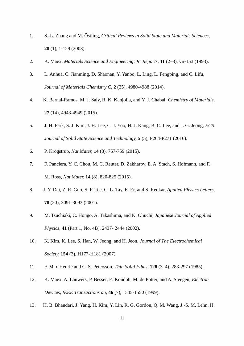
Figure 2 shows electron diffraction (ED) images of CoSi2 from transmission electron
microscopy (TEM; JEOL 2100 TEM system). ED shows that the films are polycrystalline
cubic cobalt disilicide. The speckled pattern of the diffraction rings indicates that the
specimen has relatively large grain sizes. The pattern showed part of the ring is more intense
compared to the rest, indicating a textured film. This result agreed with the XRD result.
The resistivity of CoxN and CoSi2 thin films could be obtained by measurements of the
thickness and sheet resistance. A four point probe was applied to measure the sheet resistance.
The unreacted cobalt nitrides (if any) on top of the formed CoSi2 were removed by a dilute
sulfuric acid solution at 50 °C before the measurements. A scanning electron microscope
(SEM) was used to measure the physical thicknesses. An as-deposited 30 nm CoxN film on a
Si (100) substrate generated around 120 nm of CoSi2 by in-situ annealing at 700 °C (Figure
5). The formed polycrystalline CoSi2 film was composed of grains and displayed thickness
variation in the field of view as observed in SEM image (Figure 5b). The interfacial
roughness between CoSi2 film and Si substrate fabricated from CVD CoxN is similar to that
from PVD Co.21
The resistivity of the CoxN films decreased from 140 µΩ·cm to 20 µΩ·cm
due to the formation of more conductive CoSi2. This value is close to reported resistivity of
CoSi2, i.e. 16~20 µΩ·cm.1

8
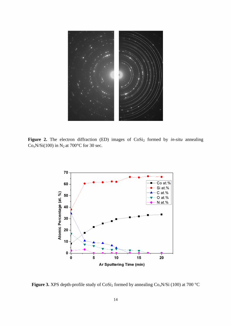
X-ray photoelectron spectroscopy (XPS) was used to measure the composition of CoSi2
films formed by annealing CoxN on Si (100) substrates at 700°C. XPS spectra taken during
argon sputtering determined the composition profiles using the Co 3p, Si 2s, C 1s, O 1s and N
1s XPS peaks. The trace of nitrogen near the surface can be attributed to a small amount of
unreacted CoxN left on the surface. Carbon and oxygen remain on the surface of the film
from air exposure. The Co:Si ratio is about 1:2 inside the film. This result confirmed that we
obtained cobalt disilicide with the expected stoichiometry after annealing CoxN/Si at 700 °C.
The CoSi2/Si interfacial roughness is an important factor that affects device performance.
We highlight here the backside sample preparation procedure to examine the CoSi2/Si
interfacial roughness by AFM (Asylum MFP-3D AFM). The initial backside sample
preparation was first proposed for SIMS sample preparation.22
We adapted this method to
remove the substrate and reveal the CoSi2 layer of interest. The CoSi2 sample was prepared
by in-situ annealing CoxN/SOI at 700 °C. We selected SOI instead of Si (100) as the substrate
owing to its built-in etch-stop layer (i.e. the buried oxide of an SOI wafer). The buried oxide
in SOI allowed selective removal of most of the SOI substrate.22
We employed a combination
of mechanic polishing, wet etching, and dry etching to reveal the CoSi2/Si interface. Wet
etching of Si-substrate is commonly performed using heated TMAH (tetramethylammonium
hydroxide) or KOH solutions.18
The wet etching is fast and easy to perform. However, the
wet etching of thick and roughly polished remaining Si inadvertently leads to the formation
of <111> faceted Si-pyramids. This formation of faceted Si-pyramids is caused by the highly
anisotropic etch rates, with etch rates of 3 crystallographic orientation being 2-3 orders of
magnitude lower than those of other major crystallographic orientations.18
Therefore, wet

9
etching cannot be used as a high-precision polishing step, and an etch-stop layer is crucial for
eliminating the roughness from the anisotropic wet-etching step. Alternatively, the Si dry
etching using XeF2 gas exhibits essentially isotropic etch rates regardless of crystallographic
orientations.18
And XeF2 dry etching has been proved to be highly selective towards CoSi2.
Thus the XeF2 dry etching process was applied to remove the thin Si remaining on top of
CoSi2.
To reveal and analyze the CoSi2/Si interfacial morphology, we adopted a modified
back-to-front sample preparation method, in which mechanical polishing, anisotropic
tetramethylammonium hydroxide (TMAH) wet etching, hydrofluoric acid (HF) wet etching,
and isotropic xenon difluoride (XeF2) dry etching are employed to remove the SOI substrate
from the back side to expose the CoSi2/Si interface, as schematically illustrated in Figure 4.
Note that for all roughness studies, “interface” is defined as the interface between CoSix and
Si, while “surface” is defined as the other side of the CoSix film. And the surface roughness
was analyzed before mounting the sample upside down onto the substrate by epoxy. Based on
the AFM image and rms results shown in Figure 5 and Table 1, the CoSi formed at 600°C
showed a surface roughness (10.1 nm) of 9.2 % of the silicide thickness (110 nm), and the
interface roughness (13.2 nm) was 12.0 % of the silicide thickness (110 nm). When
CoxN/SOI was annealed at 700°C in N2, stoichiometric CoSi2 was formed. The surface
roughness of the resulting CoSi2 was determined to be around 10.3 % (12.3 nm) of the
silicide thickness (120 nm), while the interface roughness is 7.6 % (9.1 nm) of the silicide
thickness (120 nm). Comparing the samples annealed at 600 oC and 700
oC, the surface
roughness of CoSix/Si did not change much while the CoSix/Si interfacial roughness is

10
substantially reduced after conversion of CoSi to CoSi2 at 700°C. This is because CoSi2
(cubic, lattice constant a= 5.36 Å) has a smaller lattice mismatch with Si (cubic, a= 5.54 Å),
compared with CoSi (cubic, a= 4.45 Å).
Conclusions
We successfully evaluated the CoSi2/Si interfacial roughness quantitatively by a backside
sample preparation procedure. We obtained stoichiometric cobalt disilicide, which has low
interfacial roughness because of its small lattice mismatch with Si, by in-situ rapid thermal
annealing CVD-CoxN at 700°C in N2. The backside sample preparation utilized a
combination of mechanical polishing, wet etching and dry etching to expose the CoSi2/Si
interface for AFM measurements. This approach provides a robust and reliable procedure to
acquire quantitative morphological information about silicon-silicide interfaces, which can
serve as an important assessment method for modern silicidation and metallization processes.
Acknowledgments
The authors thank Dr. Qing Min Wang, Dr. Jean-Sebastien Lehn, Dr. Huazhi Li and
Dr. Deo Shenai for helpful discussions, and for their work to synthesize the cobalt
amidinate precursor used in this work at Dow Chemical Company. This work was
performed in part at the Center for Nanoscale Systems (CNS) at Harvard University, a
member of the National Nanotechnology Infrastructure Network (NNIN), which was
supported by NSF award no. ECS-0335765.
References
11
1. S.-L. Zhang and M. Östling, Critical Reviews in Solid State and Materials Sciences,
28 (1), 1-129 (2003).
2. K. Maex, Materials Science and Engineering: R: Reports, 11 (2–3), vii-153 (1993).
3. L. Anhua, C. Jianming, D. Shaonan, Y. Yanbo, L. Ling, L. Fengping, and C. Lifu,
Journal of Materials Chemistry C, 2 (25), 4980-4988 (2014).
4. K. Bernal-Ramos, M. J. Saly, R. K. Kanjolia, and Y. J. Chabal, Chemistry of Materials,
27 (14), 4943-4949 (2015).
5. J. H. Park, S. J. Kim, J. H. Lee, C. J. Yoo, H. J. Kang, B. C. Lee, and J. G. Jeong, ECS
Journal of Solid State Science and Technology, 5 (5), P264-P271 (2016).
6. P. Krogstrup, Nat Mater, 14 (8), 757-759 (2015).
7. F. Panciera, Y. C. Chou, M. C. Reuter, D. Zakharov, E. A. Stach, S. Hofmann, and F.
M. Ross, Nat Mater, 14 (8), 820-825 (2015).
8. J. Y. Dai, Z. R. Guo, S. F. Tee, C. L. Tay, E. Er, and S. Redkar, Applied Physics Letters,
78 (20), 3091-3093 (2001).
9. M. Tsuchiaki, C. Hongo, A. Takashima, and K. Ohuchi, Japanese Journal of Applied
Physics, 41 (Part 1, No. 4B), 2437- 2444 (2002).
10. K. Kim, K. Lee, S. Han, W. Jeong, and H. Jeon, Journal of The Electrochemical
Society, 154 (3), H177-H181 (2007).
11. F. M. d'Heurle and C. S. Petersson, Thin Solid Films, 128 (3–4), 283-297 (1985).
12. K. Maex, A. Lauwers, P. Besser, E. Kondoh, M. de Potter, and A. Steegen, Electron
Devices, IEEE Transactions on, 46 (7), 1545-1550 (1999).
13. H. B. Bhandari, J. Yang, H. Kim, Y. Lin, R. G. Gordon, Q. M. Wang, J.-S. M. Lehn, H.

12
Li, and D. Shenai, ECS Journal of Solid State Science and Technology, 1 (5),
N79-N84 (2012).
14. J. Yang, K. Li, J. Feng, and R. G. Gordon, Journal of Materials Chemistry C, 3 (46),
12098-12106 (2015).
15. J. Feng, X. Gong, X. Lou, and R. G. Gordon, ACS Applied Materials & Interfaces, 9
(12), 10914-10920 (2017).
16. H. Li, G. Vereecke, K. Maex, and L. Froyen, Journal of The Electrochemical Society,
148 (6), G344-G354 (2001).
17. N.-S. Kim, C. Han-Seob, N.-K. Sung, R. Hyuk-Hyun, K.-S. Youn, and L. Won-Gyu,
Journal of Vacuum Science & Technology A: Vacuum, Surfaces, and Films, 20 (4),
1171-1176 (2002).
18. G. T. A. Kovacs, N. I. Maluf, and K. E. Petersen, Proceedings of the IEEE, 86 (8),
1536-1551 (1998).
19. S. I. Kim, S. R. Lee, J. H. Park, and B. T. Ahn, Journal of The Electrochemical
Society, 153 (5), G506-G510 (2006).
20. Bulle, x, C. W. T. Lieuwma, A. H. van Ommen, J. Hornstra, and C. N. A. M. Aussems,
Journal of Applied Physics, 71 (5), 2211-2224 (1992).
21. C.-J. Chiou, S.-P. Chiu, J.-J. Lin, and Y.-C. Chou, CrystEngComm, 17 (23),
4276-4280 (2015).
22. M. J. P. Hopstaken, C. Cabral, D. Pfeiffer, C. Molella, and P. Ronsheim, AIP
Conference Proceedings, 1173 (1), 94-98 (2009).

13
Figure 1. The XRD spectra of the as-deposited CoxN/Si (100) and the films after in-situ
annealing under 1 Torr of N2 at various temperatures (Ta = 500°C, 600°C, 700°C) for 30 s.
20 40 60 80
0
200
400
In
ten
sity (
a.u
)
2 Theta (degree)
Ta=500 °C
As-Dep
CoSi (211)
CoSi (210)
Co4N (200) Co
4N (111)
CoSi2(220)
CoSi2 (111)
Ta=600°C
Ta=700°C
CoSi2(311)
CoSi2(400)
Ta=600 oC
14
Figure 2. The electron diffraction (ED) images of CoSi2 formed by in-situ annealing
CoxN/Si(100) in N2 at 700°C for 30 sec.
Figure 3. XPS depth-profile study of CoSi2 formed by annealing CoxN/Si (100) at 700 °C

15
Figure 4. Schematic representation of consecutive steps in backside sample preparation
procedure to reveal CoSi2/Si interface: Sample is prepared by annealing CoxN on SOI
substrate at 700 °C to form CoSi2 on SOI. (a) Sample is invert and fixed on a support glass
substrate of approximately same size. (b) Sample after grinding the backside substrate with
SiC sand paper (600 - 1200 grit) to reduce substrate thickness down to below 100 µm. (c)
Sample after TMAH wet etching to selectively remove the residual silicon substrate. (d)
Sample after a dilute HF etching to remove the exposed buried oxide. (e) Sample after dry
XeF2 etching to selectively remove the residual unreacted silicon, leaving the CoSi2 surface
ready for AFM measurements.

16
Figure 5. (a-b) Cross-section SEM images of silicided SOI substrates; (c-d) Measurement of
CoSi2/Si interfacial roughness by AFM. CoSi2 is produced by annealing CVD CoxN film at
700 °C in N2.
Table 1. Cobalt silicide roughness of both surface and interface at different silicidation
temperatures. Note: For roughness study, “interface” is defined as the interface between
CoSix and Si; “surface” is defined as the other side of CoSix, which was analyzed before
mounting the sample upside down onto the substrate by epoxy.
Annealing
Temperature (oC)
Silicide
Thickness (nm)
Surface Roughness Interface Roughness
rms (nm) Percentage rms (nm) Percentage
600 110 10.1 9.2% 13.2 12.0%
700 120 12.3 10.3% 9.1 7.6%
700 oC
600 oC 700
oC
Si Si
SiO2 SiO2
Si Si
CoSix CoSix
600 oC