Embed Size (px)
Citation preview

FUJITSU FRAM
Quality & Reliability
FUJITSU SEMICONDUCTOR2010.9
For further information please contact:
North and South AmericaFUJITSU SEMICONDUCTOR AMERICA, INC.1250 E. Arques Avenue, M/S 333Sunnyvale, CA 94085-5401, U.S.A.Tel: +1-408-737-5600 Fax: +1-408-737-5999http://us.fujitsu.com/micro/
EuropeFUJITSU SEMICONDUCTOR EUROPE GmbHPittlerstrasse 47, 63225 Langen, GermanyTel: +49-6103-690-0 Fax: +49-6103-690-122http://emea.fujitsu.com/semiconductor/
KoreaFUJITSU SEMICONDUCTOR KOREA LTD.206 Kosmo Tower Building, 1002 Daechi-Dong,Gangnam-Gu, Seoul 135-280, Republic of KoreaTel: +82-2-3484-7100 Fax: +82-2-3484-7111http://kr.fujitsu.com/fmk/
Asia PacificFUJITSU SEMICONDUCTOR ASIA PTE. LTD.151 Lorong Chuan, #05-08 New Tech Park 556741 SingaporeTel : +65-6281-0770 Fax : +65-6281-0220http://www.fujitsu.com/sg/services/micro/semiconductor/
FUJITSU SEMICONDUCTOR SHANGHAI CO., LTD.Rm. 3102, Bund Center, No.222 Yan An Road (E),Shanghai 200002, ChinaTel : +86-21-6146-3688 Fax : +86-21-6335-1605http://cn.fujitsu.com/fss/
FUJITSU SEMICONDUCTOR PACIFIC ASIA LTD.10/F., World Commerce Centre, 11 Canton Road,Tsimshatsui, Kowloon, Hong KongTel : +852-2377-0226 Fax : +852-2376-3269http://cn.fujitsu.com/fsp/
Specifications are subject to change without notice. For further information please contact each office.
All Rights Reserved.The contents of this document are subject to change without notice.Customers are advised to consult with sales representatives before ordering.The information, such as descriptions of function and application circuit examples, in this document are presented solely for the purpose of reference to show examples of operations and uses of FUJITSU SEMICONDUCTOR device; FUJITSU SEMICONDUCTOR does not warrant proper operation of the device with respect to use based on such information. When you develop equipment incorporating the device based on such information, you must assume any responsibility arising out of such use of the information.FUJITSU SEMICONDUCTOR assumes no liability for any damages whatsoever arising out of the use of the information.Any information in this document, including descriptions of function and schematic diagrams, shall not be construed as license of the use or exercise of any intellectual property right, such as patent right or copyright, or any other right of FUJITSU SEMICONDUCTOR or any third party or does FUJITSU SEMICONDUCTOR warrant non-infringement of any third-party's intellectual property right or other right by using such information. FUJITSU SEMICONDUCTOR assumes no liability for any infringement of the intellectual property rights or other rights of third parties which would result from the use of information contained herein.The products described in this document are designed, developed and manufactured as contemplated for general use, including without limitation, ordinary industrial use, general office use, personal use, and household use, but are not designed, developed and manufactured as contemplated (1) for use accompanying fatal risks or dangers that, unless extremely high safety is secured, could have a serious effect to the public, and could lead directly to death, personal injury, severe physical damage or other loss (i.e., nuclear reaction control in nuclear facility, aircraft flight control, air traffic control, mass transport control, medical life support system, missile launch control in weapon system), or (2) for use requiring extremely high reliability (i.e., submersible repeater and artificial satellite).Please note that FUJITSU SEMICONDUCTOR will not be liable against you and/or any third party for any claims or damages arising in connection with above-mentioned uses of the products.Any semiconductor devices have an inherent chance of failure. You must protect against injury, damage or loss from such failures by incorporating safety design measures into your facility and equipment such as redundancy, fire protection, and prevention of overcurrent levels and other abnormal operating conditions.Exportation/release of any products described in this document may require necessary procedures in accordance with the regulations of the Foreign Exchange and Foreign Trade Control Law of Japan and/or US export control laws.The company names and brand names herein are the trademarks or registered trademarks of their respective owners.
FUJITSU SEMICONDUCTOR LIMITEDNomura Fudosan Shin-yokohama Bldg. 10-23, Shin-yokohama 2-Chome,Kohoku-ku Yokohama Kanagawa 222-0033, JapanTel: +81-45-415-5858http://jp.fujitsu.com/fsl/en/
© 2007-2010 FUJITSU SEMICONDUCTOR LIMITED Printed in JapanAD00-00015-4E September, 2010Edited: Sales Promotion Department

Table of Contents
What is FRAM? 3
Features ■ FRAM cell configurations 3
■ Cell operating principals 5
■ Writing and reading data to cells 7
■ Feature comparison between FRAM and other memories 9
Reliability 11
■ Retention 11
■ Fatigue 13
■ Retention after fatigue 14
Q u a l i t y & Re l i a b i l i t y
In 1966, Fujitsu began a company-wide movement towards high reliability.
While preparing for this movement, then-president Kanjiro Okada
summarized his thoughts on the issue with the words
“Keeping cost efficiency and keeping delivery dates are important, but
these are meaningless if quality is low.
Quality precedes everything.”
These words summarize Fujitsu’s unwavering commitment to quality.
“Quality speaks for itself - no matter where you go”Motto of the late president Fujitsu Kanjiro Okada

3 4
Q u a l i t y & Re l i a b i l i t y
■ FRAM cell configurations
The structures that are used to integrate ferroelectric film into
non-volatile memory cells can be principally divided into the two
types of (1) 1T1C (2T2C), and (2) MFIS-FET. Although each of
these offer individual features, the type that is currently used in
products is 1T1C (2T2C).
(1) 1T1C (2T2C): 1Transistor - 1Capacitor (2Tr/2Cap)
This structure is the same as a DRAM cell, and is composed of a
capacitor (C) for storing the charge that holds the data, and a
transistor (T) for accessing the data. In a DRAM cell, the capacitor
material used to store the charge is a paraelectric film such as
silicon oxide or silicon nitride. In FRAM, however, this is replaced
by a ferroelectric film. Therefore, FRAM technologies that use this
cell configuration are similar to DRAM technology, and so can be
integrated relatively easily.
The procedure for reading the cell data is to apply an electrical
potential to the cell, and then read the polarization charge that
occurs if the polarization changes (refer to "Reading and
writing data to cells" for details). One unavoidable result of
this is that the read operation is a destructive read that destroys the
stored cell data with each read cycle, requiring the data to be
rewritten in the same cycle.
Currently, 1T1C (2T2C) cells are fabricated in the planar
structure shown in Figure 1.
(2) MFSFET: Metal Ferroelectric Insulator Semiconductor FET
This configuration is also called the 1T type, and can be imple-
mented by changing the gate oxide film of a transistor from silicon
oxide film into the ferroelectric film.
Data is written to the cell by applying a potential between the gate
electrode and the substrate to reverse the polarity of the ferroelec-
tric film. Data is read by using the fact that the threshold voltage of
the transistor changes depending on the polarization direction.
The cell data is able to be retrieved by reading the magnitude of the
drain current when a specific gate voltage is applied, with the
magnitude corresponding to the polarization direction. This cell
configuration therefore shares similarities with E2PROM and flash
memory technologies. Furthermore, the main benefits of this cell
type are that data can be read non-destructively, and that the area of
the cell is small.
However, due to crystal defects and other problems at the interface
between the silicon substrate and the ferroelectric film, it is difficult
to stably on uniformity control the threshold voltage of the transis-
tor. Furthermore, the properties of the ferroelectric film may
become severely degraded to the point where non-volatility is lost,
and so this type of cell is currently under development. Although
MFMIS (Metal Ferroelectric Metal Insulator Semiconductor), in
which the ferroelectric film is grown above a floating gate, has
been proposed to resolve these problems, the dielectric constant of
the ferroelectric film is several hundred times greater than silicon
oxide, creating the problem of lower levels of polarization due to
voltage division effects. There is also a problem of the difficulty of
integration. These problems represent challenges for the future.
FRAM is a new type of non-conventional semiconductor device. This section explains the design and operating principals of FRAM, and also describes the inherent reliability of FRAM.
FeaturesWhat is FRAM?FRAM is an abbreviation of Ferroelectric Random
Access Memory. FRAM is a type of memory that
utilizes the polarization of ferroelectric materials
(a property whereby a charge remains even
when the applied potential is removed) to store
data. FRAM is also called FeRAM.
Spontaneous polarization is a phenomenon that
occurs in ferroelectric films whereby the direction
of polarization can be reversed or switched by the
direction of an applied electric field. In FRAM, this
polarization reversal or switching is used as a
memory storage function.
FRAM is able to offer non-volatile data storage by
using ferroelectric material in the memory cells.
FRAM can also be rewritten quickly and
frequently, and therefore combines the features
of both RAM and ROM.
Furthermore, read and write operations can be
performed at low voltages, making FRAM an
ideal memory for mobile devices that demand low
power consumption.
FRAM - A new type of semiconductor device that uses a ferroelectric film
Figure 1. Cross-sectional diagram of an FRAM memory cell (1T1C, 2T2C)
Bit line
Ferroelectric film
Upper electrode
Plug
Word selection line
Lower electrode
Metal 2
Metal 3
Metal 1
5 6
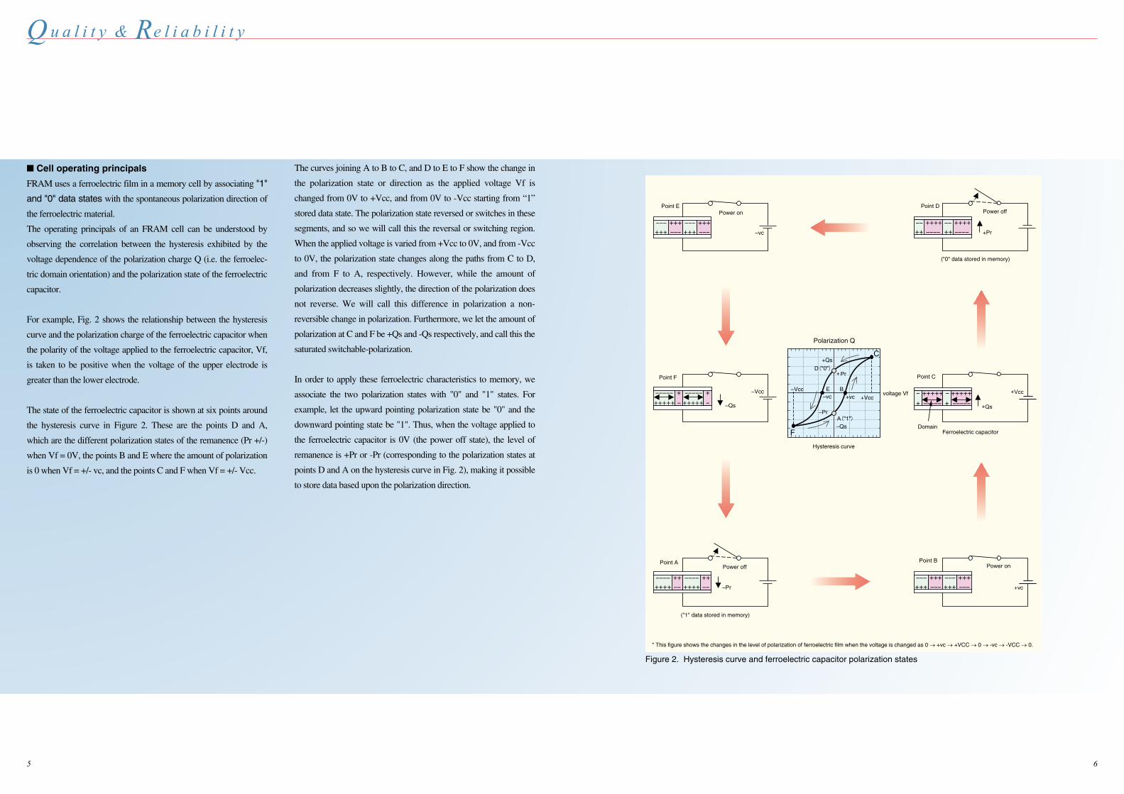
■ Cell operating principals
FRAM uses a ferroelectric film in a memory cell by associating "1"
and "0" data states with the spontaneous polarization direction of
the ferroelectric material.
The operating principals of an FRAM cell can be understood by
observing the correlation between the hysteresis exhibited by the
voltage dependence of the polarization charge Q (i.e. the ferroelec-
tric domain orientation) and the polarization state of the ferroelectric
capacitor.
For example, Fig. 2 shows the relationship between the hysteresis
curve and the polarization charge of the ferroelectric capacitor when
the polarity of the voltage applied to the ferroelectric capacitor, Vf,
is taken to be positive when the voltage of the upper electrode is
greater than the lower electrode.
The state of the ferroelectric capacitor is shown at six points around
the hysteresis curve in Figure 2. These are the points D and A,
which are the different polarization states of the remanence (Pr +/-)
when Vf = 0V, the points B and E where the amount of polarization
is 0 when Vf = +/- vc, and the points C and F when Vf = +/- Vcc.
The curves joining A to B to C, and D to E to F show the change in
the polarization state or direction as the applied voltage Vf is
changed from 0V to +Vcc, and from 0V to -Vcc starting from “1”
stored data state. The polarization state reversed or switches in these
segments, and so we will call this the reversal or switching region.
When the applied voltage is varied from +Vcc to 0V, and from -Vcc
to 0V, the polarization state changes along the paths from C to D,
and from F to A, respectively. However, while the amount of
polarization decreases slightly, the direction of the polarization does
not reverse. We will call this difference in polarization a non-
reversible change in polarization. Furthermore, we let the amount of
polarization at C and F be +Qs and -Qs respectively, and call this the
saturated switchable-polarization.
In order to apply these ferroelectric characteristics to memory, we
associate the two polarization states with "0" and "1" states. For
example, let the upward pointing polarization state be "0" and the
downward pointing state be "1". Thus, when the voltage applied to
the ferroelectric capacitor is 0V (the power off state), the level of
remanence is +Pr or -Pr (corresponding to the polarization states at
points D and A on the hysteresis curve in Fig. 2), making it possible
to store data based upon the polarization direction.
Figure 2. Hysteresis curve and ferroelectric capacitor polarization states
Hysteresis curve
A("1")
+ Pr
E
C
F
–Pr
Bvoltage Vf
D("0")
+Qs
Ferroelectric capacitor
+Qs
Point C
Point BPoint A
Point F
Point E
Polarization Q
Point D
* This figure shows the changes in the level of polarization of ferroelectric film when the voltage is changed as 0 → +vc → +VCC → 0 → -vc → -VCC → 0.
Power on
Power on
Power off
Power off
–Pr
–vc
–Qs
–Vcc
("1" data stored in memory)
("0" data stored in memory)
+vc
+Vcc
+Pr
–vc +vc–Vcc
–Qs
+Vcc
Domain
Q u a l i t y & Re l i a b i l i t y
7 8
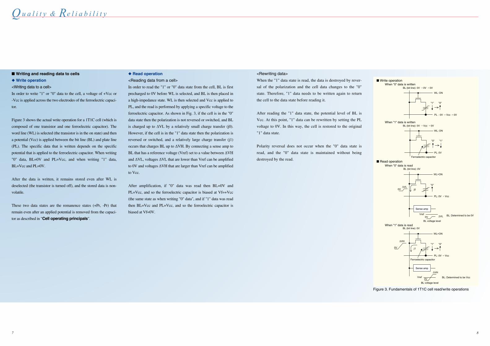
■ Writing and reading data to cells
◆ Write operation
<Writing data to a cell>
In order to write "1" or "0" data to the cell, a voltage of +Vcc or
-Vcc is applied across the two electrodes of the ferroelectric capaci-
tor.
Figure 3 shows the actual write operation for a 1T1C cell (which is
composed of one transistor and one ferroelectric capacitor). The
word line (WL) is selected (the transistor is in the on state) and then
a potential (Vcc) is applied between the bit line (BL) and plate line
(PL). The specific data that is written depends on the specific
potential that is applied to the ferroelectric capacitor. When writing
"0" data, BL=0V and PL=Vcc, and when writing "1" data,
BL=Vcc and PL=0V.
After the data is written, it remains stored even after WL is
deselected (the transistor is turned off), and the stored data is non-
volatile.
These two data states are the remanence states (+Pr, -Pr) that
remain even after an applied potential is removed from the capaci-
tor as described in "Cell operating principals".
◆ Read operation
<Reading data from a cell>
In order to read the "1" or "0" data state from the cell, BL is first
precharged to 0V before WL is selected, and BL is then placed in
a high-impedance state. WL is then selected and Vcc is applied to
PL, and the read is performed by applying a specific voltage to the
ferroelectric capacitor. As shown in Fig. 3, if the cell is in the "0"
data state then the polarization is not reversed or switched, and BL
is charged up to ΔVL by a relatively small charge transfer (j0).
However, if the cell is in the "1" data state then the polarization is
reversed or switched, and a relatively large charge transfer (j1)
occurs that charges BL up to ΔVH. By connecting a sense amp to
BL that has a reference voltage (Vref) set to a value between ΔVH
and ΔVL, voltages ΔVL that are lower than Vref can be amplified
to 0V and voltages ΔVH that are larger than Vref can be amplified
to Vcc.
After amplification, if "0" data was read then BL=0V and
PL=Vcc, and so the ferroelectric capacitor is biased at Vf=+Vcc
(the same state as when writing "0" data", and if "1" data was read
then BL=Vcc and PL=Vcc, and so the ferroelectric capacitor is
biased at Vf=0V.
<Rewriting data>
When the "1" data state is read, the data is destroyed by rever-
sal of the polarization and the cell data changes to the "0"
state. Therefore, "1" data needs to be written again to return
the cell to the data state before reading it.
After reading the "1" data state, the potential level of BL is
Vcc. At this point, "1" data can be rewritten by setting the PL
voltage to 0V. In this way, the cell is restored to the original
"1" data state.
Polarity reversal does not occur when the "0" data state is
read, and the "0" data state is maintained without being
destroyed by the read.
Figure 3. Fundamentals of 1T1C cell read/write operations
When "1" data is read
When "0" data is read
"1" "0"
WL=ON
Ferroelectric capacitor
PL: 0V → Vcc
BL (bit line): 0V
BL (bit line): 0V
"0"
WL=ON
PL: 0V → Vcc
Sense amp
j00V∆VL
0V ∆VLVref
Vref
BL voltage level
BL voltage level
j1
0V
∆VH
0V
∆VH
BL: Determined to be Vcc
BL: Determined to be 0V
Sense amp
When "1" data is written
When "0" data is written
"0"
"0"
"1"
"1"
WL:ON
WL:ON
Ferroelectric capacitor
PL:0V
PL:0V → Vcc → 0V
BL (bit line): 0V → Vcc → 0V
BL (bit line): 0V → 0V → 0V
■ Write operation
■ Read operation
Q u a l i t y & Re l i a b i l i t y

9 10
■ Feature comparison between FRAM and other memories
FRAM memory cells (the smallest units to function as data
memory) have the same structure as DRAM, consisting of a
combination of a transistor and a capacitor (see Fig. 4).
Furthermore, the use of a ferroelectric film as the capacitor
enables the data to be retained even when the power is discon-
nected, in the same way as non-volatile memory such as flash
memory. In other words, FRAM is a revolutionary semicon-
ductor memory that provides a good balance of the features of
both RAM and ROM.
Compared to the current limit on the number of times that data
can be rewritten to flash memory of 105 times, FRAM can be
rewritten over 1010 times, which is comparable to DRAM and
SRAM.
While flash memory requires that an erase operation (or sector
erase operation) is performed prior to rewriting data, FRAM
operates the same as DRAM and SRAM, and does not require
a time-consuming erase operation. Furthermore, because
refresh operations are not required in order to retain data as
they are in DRAM, FRAM offers the advantage of being non-
volatile.
Table 1 shows a comparison of the features of FRAM and
other types of memory.Figure 4. Memory cell comparison
BL
DRAM
WL
Volatile
Paraelectriccapacitor
BL
FRAM
WL
PL
Non-volatile
Ferroelectriccapacitor
FRAM
• The same structure as DRAM
• The data is retained even when the power is
disconnected (non-volatile) by using a
ferroelectric capacitor
Table 1. Feature comparison of FRAM and other types of memory
Data storage
Cell scheme
Rewriting method
Write cycle time
Number of rewrites
Write operation current
Standby current
Non-volatile
1T1C/2T2C*1
Write over
150ns
1010 (100 billion*3)
10mA (Typ.)15mA (Max.)
5µA (Typ.)50µA (Max.)
FUJITSU FRAM MRAM SRAM
Non-volatile
1T1MTJ*2
Write over
35ns
Infinite
105mA (Typ.)155mA (Max.)
9mA (Typ.)12mA (Max.)
Non-volatile
2T
Erase + Write
5ms
106 (1 million)
5mA (Max.)
2µA (Max.)
E2PROM(SPI)
Flash(NOR)
Non-volatile
1T
Sector erase + Write
10µs
105 (100,000)
20mA (Max.)
100µA (Max.)
Volatile
6T
Write over
55ns
Infinite
8mA (Typ.)
0.7µA (Typ.)3µA (Max.)
Q u a l i t y & Re l i a b i l i t y
∗ 1: 1 transistor 1 capacitor / 2 transistor 2 capacitor∗ 2: 1 transistor 1 magnetic tunnel junction∗ 3: Total number of reads and writes

11 12
■ Retention
FRAM is non-volatile memory that is able to preserve the data
that has been written without power. The ability to preserve
this data for a long period of time without the data being lost is
called "retention". In general, retention is strongly
temperature-dependent. Guaranteed retention lifetimes are
therefore subject to temperature conditions. (For example, 10
years at 70°C or less.) The following section describes the
procedure for evaluating retention and the modes of degrada-
tion.
The above procedure is repeated until a read error occurs, and the
retention lifetime is determined based upon the baking
temperature by applying the Arrhenius equation*.
The first time the data pattern is read, the data pattern that was
exposed to high temperature is read, and so this is called the SS
(Same State) read. The second data pattern read is the reverse data
pattern, and so this is called the OS (Opposite State) read.
The level of polarization of the ferroelectric is dependent on the
applied voltage as shown in Fig. 6. Retention tends to depend on
the level of polarization. Writing data using an insufficient applied
voltage therefore creates a risk of degradation of the retention.
Retention testing is therefore carried out at the minimum power
supply voltage that is guaranteed for operation in the catalog.
(1) Testing procedure
As described above, retention is highly temperature-dependent,
and so testing can be accelerated using temperature.
First, some data pattern (such as a checkerboard pattern of "0"
and "1") is written to the FRAM, and the FRAM is then left
exposed to high temperature for a fixed period of time. The
data pattern is then read to confirm that the data that was
originally written has been preserved. Next, a data pattern that
is the reverse of the data pattern that was originally written (the
"0" and "1" states are swapped) is written, and a check is
performed that the data can be read correctly. Finally, the data
pattern that was first written is written again, and the FRAM is
again exposed to a high temperature.
(2) Degradation modes
The retention is degraded by two modes: depolarization and
imprinting. These two degradation modes can be detected by
testing both "SS" reads and "OS" reads.
a) Depolarization by heat
Depolarization is a phenomenon where the direction of polarization
reverses and the level of remanence is reduced (+Pr and -Pr drop),
as shown in Fig. 7.
Because FRAM is read by detecting the level of polarization, a
decrease in the remanence leads to read errors. The depolarization
phenomenon becomes more pronounced as the temperature
increases. At a sufficiently high temperature, depolarization occurs
in a matter of seconds, and this is followed by virtually no change
loss irrespective of how much time passes.
Degradation of retention due to depolarization is revealed by errors
in the "SS"read.
Depolarization is a property observed in all ferroelectrics in
response to high temperature, and is not physical degradation. If
data is again written at normal operating temperatures, the polariza-
tion is restored.
ReliabilityBecause FRAM devices use a ferroelectric film,
the reliability of the ferroelectric film needs to be
considered in addition to the reliability that is
required of general semiconductor devices.
One of the problems with the reliability of ferro-
electric films is a loss of polarization due to deg-
radation phenomena. Degradation of polariza-
tion levels occurs due to various reasons and
the effects of polarization loss is observed when
measuring retention and fatigue. At Fujitsu, the
Test Element Group (TEG) performs evalua-
tions on products to ensure the reliability of
FRAM as described above.
Figure 5. Testing procedure
Write data pattern (SS data)
Expose to high temperature
Read SS
Write OS
Read OS
Write SS
∗ τ∝Exp (Ea/kT) τ: Retention lifetime Ea: Activation energy k: Boltzmann constant T: Absolute temperature
Figure 6. Graph of polarization saturation versus applied voltage
Applied Voltage [V]
Sw
itchi
ng C
harg
e [µ
C/c
m2 ]
35
30
25
20
15
10
5
0
10 2 3 4 5 6
Figure 7. Loss of polarization due to high temperature exposure or thermal depolarization
Polarization Q
Voltage Vf
Initial characteristicsChange after baking athigh temperature
Q u a l i t y & Re l i a b i l i t y
13 14
b) Degradation by imprint
Imprint is a phenomenon where the polarization is gradually
reduced after storage over a period of time, and the polarization
becomes difficult to reverse.
When imprint occurs, it becomes difficult to write the reverse data.
Imprint can be observed when viewing the hysteresis characteris-
tics as a phenomenon where the hysteresis curve is shifted to the
left or right, as shown in Fig. 8. (A shift in the coercive voltage
(+Vc, -Vc))
The "OS" read that is performed in the evaluation procedure in Fig.
5 is to check for this degradation mode.
This is a physical phenomenon which is difficult to reverse.
■ Fatigue
Fatigue is a phenomenon where the level of polarization decreases
as the ferroelectric polarization is repeatedly reversed.
Fatigue occurs during both read and write cycles, it also occurs
during read cycles. This is because reading an FRAM memory cell
is a destructive read that involves the sequence of operations of
reading and then rewriting the data, the same as in DRAM, and
therefore polarization reversal occurs. (See "Writing and read-
ing data to cells".)
The guaranteed number of FRAM rewrite cycles is therefore not
based on read/write cycles, but is defined as the total number of
accesses to each individual memory cell.
The following section describes the method for evaluating fatigue
and the degradation modes.
(1) Testing procedure
Fatigue testing is performed by applying fatigue bipolar stress,
which basically involves repeatedly performing read or write
operations a specified number of times, and then checking whether
the FRAM operates normally.
As an example, the amount of time required for fatigue stressing of
64 kbit FRAM memory cells in an 8 kword x 8 bit configuration
when the operation cycle time is 250 ns can be calculated. In this
case, 8 bits can be simultaneously stressed at the same time, and so
8 kcycles are required to write to all of the memory cells once. The
amount of time needed to carry out a specific number of stress
cycles is therefore given as follows.
108 times: 250 ns × 8,192 × 108 = Approx. 57 hours
1010 times: " × 1010 = Approx. 237 days
1012 times: " × 1012 = Approx. 65 years
As the above example shows, it becomes difficult to actually carry
out fatigue testing for more than a certain number of rewrites.
To overcome this, the testing time can be reduced using the
following methods.
a) Accelerated by increasing the applied voltage and temperature
b) Limit the number of cells being stressed (sample testing)
c) Apply stress to multiple cells at the same time (simultaneous testing)
(2) Degradation modes
The degradation in the remanence as shown in Fig. 9 is observed
after a certain number of repetitions of read or write operations.
Although this resembles the degradation by thermal depolarization
at elevated temperature, the polarization does not return to the
previous level when rewritten.
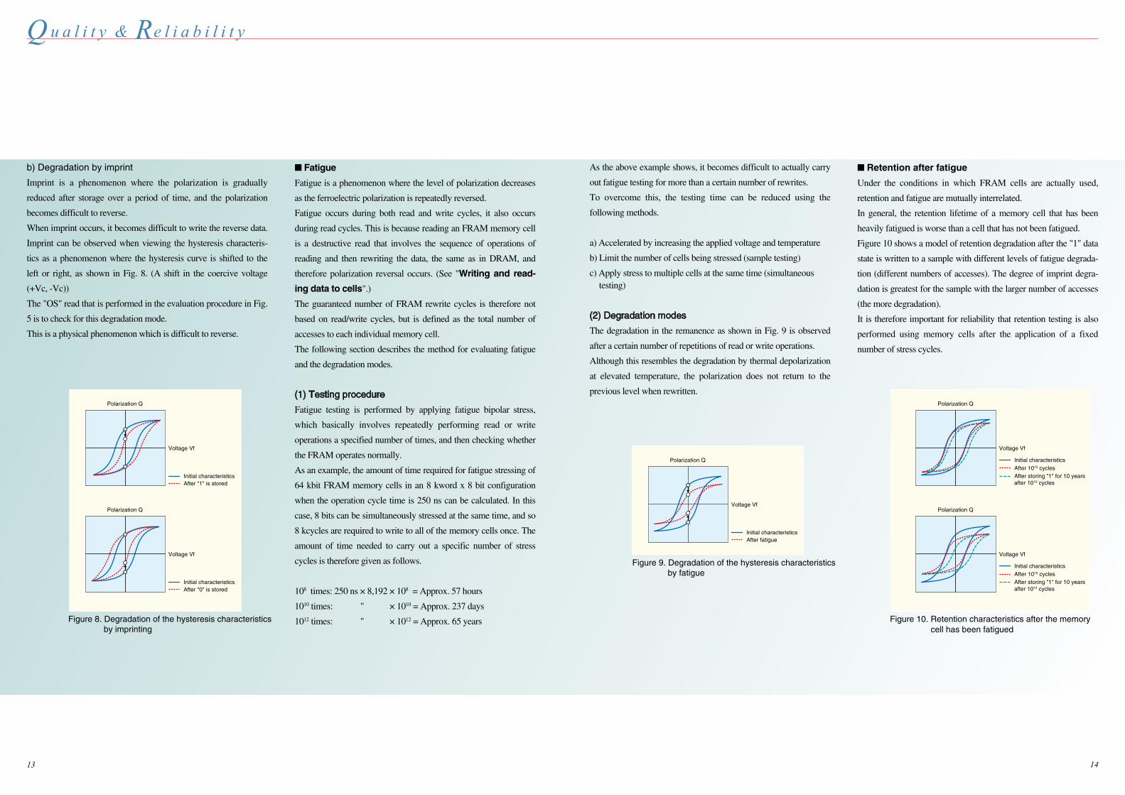
■ Retention after fatigue
Under the conditions in which FRAM cells are actually used,
retention and fatigue are mutually interrelated.
In general, the retention lifetime of a memory cell that has been
heavily fatigued is worse than a cell that has not been fatigued.
Figure 10 shows a model of retention degradation after the "1" data
state is written to a sample with different levels of fatigue degrada-
tion (different numbers of accesses). The degree of imprint degra-
dation is greatest for the sample with the larger number of accesses
(the more degradation).
It is therefore important for reliability that retention testing is also
performed using memory cells after the application of a fixed
number of stress cycles.
Polarization Q
Voltage Vf
Figure 9. Degradation of the hysteresis characteristics by fatigue
Initial characteristicsAfter fatigue
Figure 10. Retention characteristics after the memory cell has been fatigued
Polarization Q
Voltage Vf
Initial characteristicsAfter 1010 cyclesAfter storing "1" for 10 yearsafter 1010 cycles
Polarization Q
Voltage Vf
Initial characteristicsAfter 1012 cyclesAfter storing "1" for 10 yearsafter 1012 cycles
Figure 8. Degradation of the hysteresis characteristics by imprinting
Polarization Q
Voltage Vf
Initial characteristicsAfter "0" is stored
Polarization Q
Voltage Vf
Initial characteristicsAfter "1" is stored
Q u a l i t y & Re l i a b i l i t y