Embed Size (px)
Citation preview

D-A233 110 7-
RADC-TR-90-405Final Technical ReportDecember 1990
QUALIFICATION PROCEDURESFOR VHSICIVLSI
GE Aerospace DTCThomas A. Baumes ELECTE
MAR 18 1991~D
APPROVED FOR PUBLIC RELEASE, DISTRIBUTION UNLIMITED
Rome Air Development CenterAir Force Systems Command
Griffiss Air Force Base, NY 13441-5700
91 3 14 019

This report has been reviewed by the RADC Public Affairs Division (PA)
and is releasable to the National Technical Information Service (NTIS). At
NTIS it will be releasable to the general public, including foreign nations.
RADC-TR-90-405 has been reviewed and is approved for publication.
APPROVED: Q jJ ~ v A
CHARLES G. MESSENGERProject Engineer
APPROVED: aUJOHN J. BART
Technical DirectorDirectorate of Reliability & Compatibility
FOR THE/COMMANDER:
JAMES W. HYDE, III.Directorate of Plans & Programs
If your address has changed or if you wish to be removed from the RADC mailing
list, or if the addressee is no longer employed by your organization, pleasenotify RADC (RBRA) Griffiss AFB NY 13441-5700. This will assist us in main-taining a current mailing list.
Do not return copies of this report unless contractual obligations or notices
on a specific document require that it be returned.

DISCLAIMER NOTICE
THIS DOCUMENT IS BEST
QUALITY AVAILABLE. THE COPY
FURNISHED TO DTIC CONTAINED
A SIGNIFICANT NUMBER OF
PAGES WHICH DO NOT
REPRODUCE LEGIBLY.

Form ApprovedREPORT DOCUMENTATION PAGE OMB No. 0704-0188Ptbk (corxtro burdi, for r-ys co ict i fonw k y bTresthted to wr g hor pw respa ne, 'z g the te for rriw~rg kwu1o se dwV g r .ast a Sources,goisr W- 'wtnamr dne needdV cn kg wiwwe, thde cfoI korn Skldn d c s rrgu g ten bidm ee or W1 1± #spd d scolect0n d rforrtabm incL- g 9ajpsdons for redcing tt-s buied, to Washrgoc Hwkputers SwAcm Dkectorae for Horar=, Operis andReports. 1215 JeffersonDws Hg wy Sure 1204 A,*Vb VA 2222-432 wdtote Office d Mwpenurtf d Bu.gK Pap woc Redxton Prdect (0704-O18M, Was'r o , DC 205
1. AGENCY USE ONLY (Leave Blank) 2- REPORT DATE 3. REPORT TYPE AND DATES COVERED
IDecember 1990 Sep 86 to Aug 89
4. TITLE AND SUBTITLE & FUNDING NUMBERS
QUALIFICATION PROCEDURES FOR VHSIC/VLSI C - F30602-86-C-0172PE - 63452F
.AUTHOR(S) PR - 2700TA - 02
Thomas A. Baumes WIU - 23
7. PERFORMING ORGANIZATION NAME(S) AND ADDRESS(ES) 8. PERFORMING ORGANIZATION
GE Aerospace REPORT NUMBER
French RoadUtica NY 13503 N/A
9. SPONSORING/MONITORING AGENCY NAME(S) AND ADDRE$(ES) 1. SPONSORINGMONITORING
Rome Air Development Center (RBRA) AGENCY REPORT NUMBER
Griffiss AFB NY 13441-5700 RADC-TR-90-405
11. SUPPLEMENTARY NOTES
RADC Project E.agineer: Charles G. Messenger/RBRA/(315) 330-2047
12a. DISTRIBUTIONAVAILABILITY STATEMENT 12b. DISTRIBUTION CODE
Approved for public release; distribution unlimited.
13. ABSTRACT(Mm 2w-rds)
This program developed, outlined, refined and verified the test methodology andqualification criteria and procedures to be used to ensure the integrity and reliabil-ity of microcircuit devices designed for insertion into military systems. A major
portion of the criteria and procedures, reflected herein, enables a significantreduction in time and cost of the microcircuit Quality/Reliability Assurance process
by adressing up front simulations during design prior to commitment, complex andexpensive manufacturing processes with in-line quality processes controlled by a SPC
(Statistical Process Control) program and ongoing QA Program using their TRB (Tech-
nology Review Board) and SEC (Standard Evaluation Circuit) programs.
14. SUBJECT TERMS 15 NUMBER OF PAGESMicrocircuits, QNL, Qualification, Quality, Reliability,
Generic Qualification, Integrated Circuits, VHSIC, VLSI 16 PRICE CODE
17. SECURITY CLASSIFICATION 18. SECURITY CLAS.IFICATION 19. SECURITY CLASSIFICATION 20. UMITATION OF ABSTRACTOF REPORT OF THIS PAGE OF ABSTRACTUNCLASSIFIED UNCLASSIFIED UNCLASSIFIED UL
NSN 754-O1.28D-5500 Stwrird Form 298 (Rev 2 89)Pfesorbod by ANSI Std Z39-18298-102

EVALUATION
This program was sponsored by the VHSIC program office to investigate anddevelop an alternative approach for qualification of complex microcircuits. Toaddress the technical issues related to a process oriented qualification approach,the contractor organized an Industry Coordinating Working Group (ICWG) whichwas divided into four microcircuit manufacturing disciplines: design, fabrication,assembly, and test. The ICWG spawned and refined several key concepts, such asTechnology Review Board (TRB), Technology Characterization Vehicle (TCV) andStandard Evaluation Circuit (SEC). These concepts were then integrated withTotal Quality Management (TQM) principles and formulated the basis for theQualified Manufacturer's List (QML).
The final output of the program was a DOD specification MIL-I-38535, "GeneralSpecification for Integrated Circuit Manufacturing." This document details therequirements a manufacturer must address in order to be listed on the QML.Presently, several refinements to the requirements are ongoing. These refinementsare addressing issues related to radiation hardness and third party design. Overall,this program was very successful and providesd the DOD with an approach toqualifying high complexity Application Specific Integrated Circuits (ASIC) forsys, usage.
CHARLES G. MESSENGER
Accion ,
By.................
D i t C .. .IJI
.3.
iy .... .. ... . . . .

Contents
1. INTRODUCTION ................................................ 1-1
1.1. GENERAL ....................................................... 1-1
1.2. PROGRAM OBJECTIVE..............................................1.-1
1.3. SUMMARY OF RESULTS............................................. 1-2

Contents
2. TASK I - REVIEW OF DOCUMENTS............................... 2-1
2.1. OBJECTIVES............................................... 2-1
2.2. APPROACH................................................. 2-2
2.3. RESULTS.................................................. 2-3
2.3.1. MIL-M-38510F: General Specification for Microcircuits.........2-3
2.3.1.1. Discussion of MIL-M-38510F ................................ 2-3
2.3.1.2. Major Findings in MIL-M-38510F............................. 2-4
2.3.2. MIL-STD-883C ............................................. 2-5
2.3.2.1. Discussion of Series 1000 and 2000 Methods ................... 25
2.3.2.2. Major Findings in 1000 and 2000 Series...................... 2-5
2.3.2.3. Discussion of 3000 Series ................................. 2-8
2.3.2.4. Major Findings in 3000 Series ............................. 2-10
2.3.2.5. Discussion of 4000 Series ................................. 2-13
2.3.2.6. Major Findings in 4000 Series ............................. 2-13
2.3.2.7. Discussion of 5000 Series ................................. 2-15
2.3.2.8. Major Finding in 5000 Series .............................. 2-17
2.3.3. MIL-STD-976A............................................. 2-17
2.3.3.1. Discussion of MIL-STD-976A ................................ 2-17
2.3.3.2. Major Findings in MIL-STD-976A .............. .............. 2-18
2.3.4. MIL-STD-1331............................................. 2-18
2.3.4.1. Discussion of MIL-STD-1331 ................................ 2-18
2.3.4.2. Major Findings in MIL-STD-1331............................. 2-19
2.4. SUMMARY ................................................. 2-19

Contents
3. TASK II - INVESTIGATION ................................... 3-13.1. INTRODUCTION............................................. 3-13.2. INDUSTRY COORDINATING WORKING GROUP (ICWG) ................... 3-13.2.1. ICWG Organization......................................... 3-13.2.2. Quality Management ICWG Subcommittee........................ 3-23.2.3. Design and Test ICWG Subcommittee .......................... 3-243.2.3.1. Topics of Discussion...................................... 3-23.2.3.2. Major Results ............................................ 3-33.2.4. '.brication ICWG Subcommittee.............................. 3-53.2.4.1. TorJLS of Discussion...................................... 3-53.2.4.2. Major Results ............................................ 3-63.2.5. Assembly/Packaging ICWG Subcommittee........................ 3-93.2.5.1. Topics of Discussion...................................... 3-93.2.5.2. Major Results ............................................ 3-93.2.6. SQC/QRA ICWG Subcommittee................................. 3-123.2.6.1. Topics of Discussion ..................................... 3-123.2.6.2. Major Results............................................ 3-133.3. DRAFT OF QML REQUIREMENTS - APRIL '88 DRAFT................. 3-143.3.1. Manufacturer's QA Program Plan............................. 3-153.3.1.1. QA Program Plan-Section A................................. 3-153.3.1.2. QA Program Plan-Appendix 1 of Section A .................... 3-163.3.1.3. QA Program Plan-Section B ................................ 3-183.3.2. Self Audit .............................................. 3-183.3.2.1. Self Audit-Section A ..................................... 3-183.3.2.2. Self Audit-Appendix 1 of Section A ......................... 3-183.3.3. Technology Review Board (TRB) ............................. 3-19
3.3.3.1. Technology Review Board-Section A.......................... 3-203.3.4. Total Quality Management/Control (TQM/TQC).................. 3-23
iv

3.3.4.1. Total Quality Management/Control (TQM/TQC)-
Appendix 1 of Section A ...................................... 3-23
3.3.5. Statistical Process Control-Section A ........................ 3-23
3.3.5.1. Statistical Process Control-Appendix I of Section A .......... 3-23
3.3.5.2. Statistical Process Control-Section B ........................ 3-23
3.3.6. Standard Evaluation Circuit (SEC)-Section A .................. 3-24
3.3.6.1. Standard Evaluation Circuit (SEC)-Section A .................. 3-24
3.3.6.2. Standard Evaluation Circuit (SEC)-Appendix 1 of Section A .... 3-24
3.3.6.3. Standard Evaluation Circuit (SEC) Section B .................. 3-25
3.3.6.4. Standard Evaluation Circuit (SEC)-Appendix 1 of Section B .... 3-25
3.3.7. Quarterly Report .... ................................. 3-26
3.3.7.1. Quarterly Report-Section A ................................... 3-26
3.3.7.2. Quarterly Report-Appendix 1 of Section A ..................... 3-26
3.4. SUMMARY ...................................................... 3-26
v

Contents
4. TASK III- DEMONSTRATION AND GENERAL SUPPORT ................. 4-1
4.1. INTRODUCTION............................................. 4-1
4.2. ALPHA SITE DEMONSTRATIONS ................................. 4-1
4.2.1. Alpha Site Validation..................................... 4-2
4.2.1.1. Pre Validation Submittal .................................. 4-2
4.2.1.2. Validation Reviews........................................ 4-2
4.3. BETA SITE DEMONSTRATIONS .................................. 4-5
4.3.1. Companies Involved in Beta Sites ........................... 4-5
4.3.2. Progress ........................... ..................... 4-5
4.4. BETA SITE MEETINGS........................................ 4-5
4.5. GENERAL SUPPORT .......................................... 4-6
4.5-1. Handbook ................................................ 4-6
4.5.2. Proposed Test Methods ................................ .... 4-6
vi
Contents
5. CONCLUSIONS AND RECOMMENDATIONS ................................ 5-1
51!. CONCLUSIONS .................................................... 5-1
5.1.1. Design ......................................................... 5-1
5.1.2. Fabrication .................................................... 5-1
5.1.3. Assembly and Packaging ......................................... 5-2
5.1.4. Test ........................................................... 5-2
5.2. RECOMMENDATIONS ................................................ 5-3
Appendix A General Specification for Integrated Circuits (Microcircuits)
Manufacturing
Appendix B Proposed Test Methods for VHSIC/VLSI Generic Qualification
Appendix C Proposed Requirements to Qualify CAD Tools for VHSIC/VLSI
Devices
vii

1. iNTRODUCTION
1.1. GENERAL
In September of 1986, GE/AES, Utica, NY receivod a contract to develop
a Generic Qualification approach to microcircuit qualification that would not
only benefit the military acquisition arena but also develop a methodology of
microcircuit process control to promote the United States to a position of
supplying the nighest quality and most reliable microcircuits in the world.
This contract was awarded and administered by RADC.
In order to expand the technical team and provide expertise in the
areas of commercial and bi-polar techniques and technologies, two
subcontracts were awarded by GE to AT&T Bell Lab, Allentown PA and Honeywell
Inc, Plymouth MN.
This effort was performed in conjunction with the VHSIC Program and the
DOD effort to streamline the acquisition and costs of microcircuits used by
the DOD. The Industry Coordinating Working Group (ICWG) which included the
Government, Industry and Academia was formed to provide technical insights,
critiques, and guidance in support of this effort.
1.2. PROGRAM OBJECTIVE
This program was derived to develop a new approach to qualifying
complex microcircuits. Recent trends in military systems showed that there
was wider use of low volume, complex, application specific integrated
circuits and less reliance on high volume standard microcircuits. As a
result there was an explosive increase of nonstandard, noncertified and
nonqualified microcircuits in new systems. This raised concerns over system
logistic support, reliability and availability.
Also studies of the DOD VHSIC program suggested that it was no longer
economical to quality piece parts using existing qualification procedures,
due to the cost, complexity and relatively low quantity production of
individual VHSIC/VLSI device designs. The advent of Computer Aided Design
(CAD) tools which accurately simulate and predict device performance before
1-1

actual production allowed for more efficient and economical means of
production and testing thus allowing quality and reliability to be designed
in instead of tested in.
These issues along with the inability of the existing qualified parts
list (QPL) system to handle these new device trends were the impetus for this
program.
The objective, then, of this program was to develop a new approach to
microcircuit qualification based on process control while taking advantage of
new tools, such as Statistical Process Control (SPC) and CAD, and assure the
quality and reliability for use in military systems of those devices produced
from that process. All aspects related to microcircuit manufacturing from
design through final test were to be addressed in the new procedures.
Three tasks were defined to accomplish this objective:
o Task I - Review and Definition - review existing procedures for
applicability to VHSIC/VLSI devices.
o Task II - Investigation - research technical issues through the
establishment of an Industry Coordinating Working Group (ICWG) and
propose new procedures.
o Task III - Verification and Demonstration - verify and demonstrate
the new procedures on the contractors' manufacturing process.
Make improvements to the procedures based on the outcome of the
demonstration.
1.3. SUMMARY OF RESULTS
The Qualification Procedures for VHSCI/VLSI program resulted in the
following major accomplishments:
Existing military documents associated with microcircuit qualification
were reviewed for applicability. This review outlined several areas where
changes were necessary to facilitate the qualification of complex VHSIC/VLSI
1-2

devices in military systems. To better address these issues and develop
technical approaches, an Industry Coordinating Working Group (ICWG) was
established. The ICWG recommended a quality management oriented approach to
the problem. The contract team of GE, AT&T and Honeywell utilized many of
the proposed recommendations of the ICWG in formulating a draft procedure.
Finally, a qualification procedure document was developed, completed
and issued (on 18 Dec 1989) as MIL-I-38535, "INTEGRATED CIRCUIT
MANUFACTURING, GENERAL SPECIFICATION FOR" (see Appendix-A). The MIL-I-38535
document establishes the general procedures and the quality and reliability
assurance requirements for the manufacturing and acquisition of integrated
circuits. Key to quality and reliability assurance is the requirement for
quality management. Through quality management, a manufacturer is positioned
to provide to the marketplace a cost effective, high quality and reliable
microcircuit within the DoD acquisition requirements, as well as the
commercial requirements, as a qualified manufacturer. Also, the DoD is
ensured of the best possible integrated circuits qualified and ready for
insertion in shorter cycle times.
Alpha site demonstrations were performed by GE and AT&T to provide
confirmation of the applicability of che new procedures. Based on the
results, changes to the QML requirements were recommended and implemented in
MIL-I-38535. Following Alpha site demonstrations, Beta site meetings were
held to further enhance the requirements applicability and acceptance.
Other outputs of this program included draft versions of new test
methods for testing digital microcircuits. Also, a Manufacturing Guidelines
document was developed to provide an up-to-date index of tools which can be
utilized to improve manufacturing quality.
The particulars of these tasks are discussed in more detail in the
1-3

2. TASK I - REVIEW OF DOCUMENTS
2.1. OBJECTIVES
The objective of the review of existing MIL-STD documents was to use
the teams' awareness of existing procedures and methods to determine which
of the existing military documents require attention for implementation of
the new qualification approach for VHSIC/VLSI. The approach encouraged
utilization of that which is still relevant; identify areas that needed new
methods or procedures; and flag areas not presently covered.
The review of the documents categorized them into one of the following:
o Retain: when the document was relevant to VHSIC/VLSI and needs no
modification.
o Modify: when the document was generally useful but requires
modification for VHSIC/VLSI application, or because it required
more clarity in the definition of the procedures, or for improved
readability and/or user-friendliness.
o New: when the objectives of the document remained valid but new
methods are needed for VHSIC/VLSI applicability.
o Not applicable: when the scope of the document was not pertinent
to VHSIC/VLSI.
In addition to determining the usefulness of existing documentation,
the team sought to identify gaps. Today's qualification approach is heavily
dependent on testing of finished product, whereas the new approach seeks to
qualify the processes that yield the finished product. It was, therefore,
necessary to identify areas not covered by today's methods which will need to
be covered under the new approach. For example, the process by which ICs are
designed is minimally covered under existing procedures, buL iL will be
critical under the new approach to identify a method for assuring that design
rules are adhered to, and that CAD tools are adequate. Some new approaches
to qualification were considered by the team at the beginning of Task 1, such
2-1

as "Parametric Monitors" (PMs) for checking the electrical performance
parameters of a process and "Standard Evaluation Circuits" (SECs) which can
be used in place of the actual circuits for many of the require reliability
tests.
2.2. APPROACH
The approach taken by the Task 1 team to best meet the objectives was:
o Establish a basis for the review criteria to give commonality in
evaluation procedures.
o Assign document review responsibility on basis of expertise and
available resources.
o Coordinate document reviews with weekly and monthly status reviews
on progress.
o Summarize results and collate into four basic categories. (Not
Applicable-N/A, Modify-Mod, Modify to include surrogate-Mod*, and
Retain-Ret)
o Include plans for ICWG involvement in document review through ICWG
structuring and recruiting.
A common review sheet was prepared and distributed. The review sheet
contained three main sections providing:
o A description of what was being evaluated.
o What reliability information was gained.
o Will modification be required for VHSIC?
With each document assigned for review, subtest methods and/or
subparagraphs were partitioned and reviewed by assigned personnel.
2-2

To monitor progress and allow for continual interaction of all
functions, weekly and monthly status reviews were held. This ensured that
individual document reviewers were cognizant of concerns and accomplishments
of the entire Task 1 team.
The review sheets were then summarized and collated to provide
categorization for Task 2 follow-up review by the ICWG.
2.3. RESULTS
2.3.1. MIL-M-38510F: General Specification for Microcircuits
2.3.1.1. Discussion of MIL-M-38510F
The review of this document identified areas that were not compatible
and/or adequate to VHSIC/VLSI technology. These are detailed below:
Paragraph 3.5 - Design and Construction: This section provides
guidelines to be implemented in design. The major comment for this section
is that it does not address CAD issues. Certification and monitoring of CAD
is key to the new approach.
Paragraph 4.4.2 - Qualification (per MIL-STD-883C, Method 5005); and
Paragraph 4.5 - Quality Conformance inspection (per MIL-STD-883C, Method
5005): this document requires that Method 5005 be used on real product,
which implies high cost for low volume product such as VHSIC. In its present
form, no provision is made for the use of PMs and SECs. The new approach
will emphasize the use of PMs and SECs as a way to certify and monitor the
processes that yield the final product.
Paragraph 4.6 - Screening (per MIL-STD-883C, Method 5004): the
document requires testing of 100% of product per all the applicable tests in
Method 5004. Some of the screening procedures are not effective for
VHSIC/VLSI application. One example is the Method 2010, Internal Visual,
which has very limited application to devices with very small design
features.
2-3

Appendix A - Product Assurance Program: this appendix addresses
documentation, certification, qualification and other aspects of the product
realization flow, from design to outgoing inventory. Many of the issues
cited from the main body of the MIL-M-38510 document, apply here as well.
For example, Paragraph 20.1.1.6 - Design, Processing, Manufacturing,
Equipment, and Materials Instructions, does not address CAD, PMs, or SECs.
2.3.1.2. Major Findings in MIL-M-38510F
The major findings of this review of MIL-M-38510F are:
o Modification of the document is required for VHSIC/VLSI
application.
o CAD is not addressed.
o Some of the screening procedures are not suitable for VHSIC/VLSI
(e.g., High Power Visual Inspection).
0 Qualification and Quality Control Inspection procedures need to be
modified for VHSIC/VLSI application because: the procedures are
product, not process, oriented; no use is made of PMs or SECs; and
sampling plans assume high volume production.
o The document is complex, which makes it hard to follow, and prone
to misinterpretation.
2-4

2.3.2. MIL-STD-883C
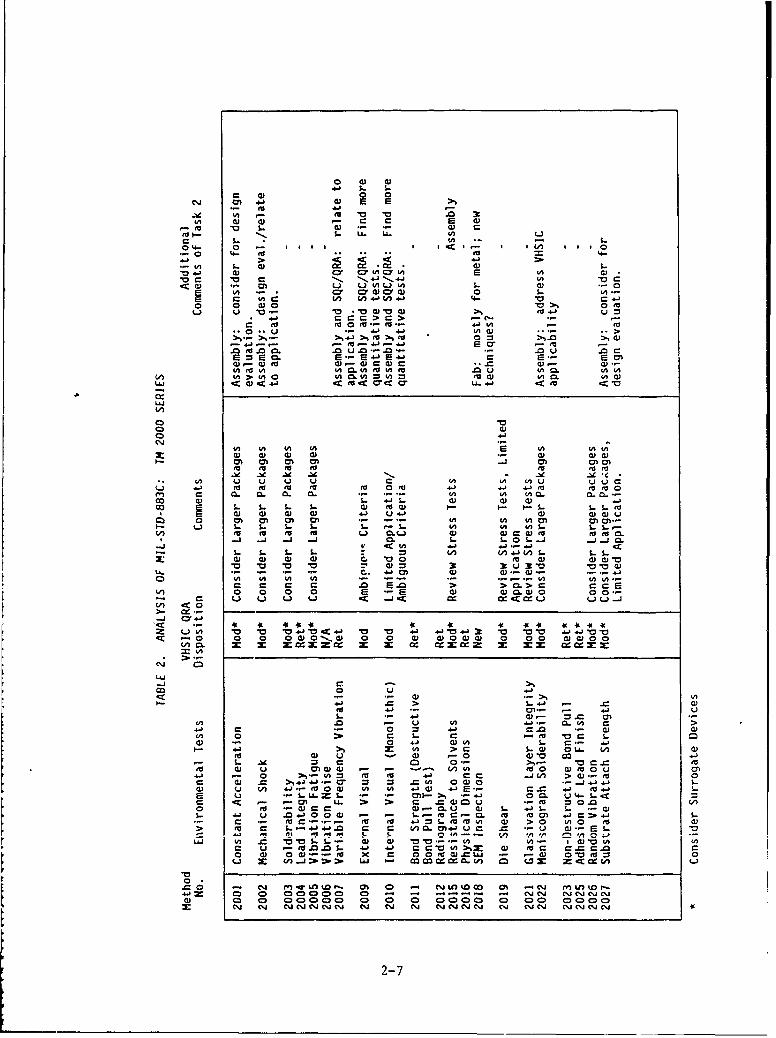
2.3.2.1. Discussion of Series 1000 and 2000 Methods
The Tables I and 2 below list the results of the review. The column
labeled "VHSIC QRA Disposition" reflects the reviewer's current thinking on
the applicability of the method to the new VHSIC QRA approach. The
"Comments" column captures the underlying reasons for the dispocition. The
column labeled "Additional Comments for Task 2" provides recommendations
and/or raises flags for the team to address during the Task 2 activity. The
footnote reference to "surrogate devices" alludes to tests being performed on
Process Monitors (PMs) or Standard Evaluation Circuits (SEC) rather than the
primary product.
2.3.2.2. Major Findings in 1000 and 2000 Series
o Most of the test methods in the 1000 and 2000 series remain
applicable, either "as is" or with modification. Some test
methods may need to be developed to properly address the QML
approach. In some cases, it is envisioned that the QML approach
may call for tests to be performed in a step of the product
realization chain replacing tests that are now performed elsewhere
downstream in the manufacturing cycle.
o Many Test Methods may require updating for:
- Use with PMs and SECs;
- Application to VHSIC/VLSI technology requirements;
- Clarification of test criteria, purpose, assumptions, and
technical references, where possible.
2-5

CC
oz U-: Uz U UCC.
Cj CW C) CI) C)-CL a) CV uC C) 'C vA ' C
m' : m 0 0 0 -' "S- (C.- 0 0 -0 0. z CL. I.- Ca m)C
0. )UC)C U (x U C) a)
(A~' >1 w w~.J U( A(
C ~ ~C . 'C c. A ( A ~ '
a) (A r cy a r - c
0 ~ ~ ar (A CS...0< ) Ln S.. a a) c a C) .
VC LI Ln V) V) <.) CZ -
(A (A (A vi(A < ) i A aCA cm 0 C'V A ' ) (An C i ) )
CL)~~' U S- S m S.
el CD a) a) C) ) 0' C ) C).)) CC.
L~J< .1- (A z "- ~ ~ U. C
o~a 4. 4) '.
o- ws C .- CS- S
'C 1) e (A (A)u 0(A (A vi ) C .0=C 0 C C
SV V (A w- 0a ) S. 0M0 m 0coVC) 0) C.) C.-C a LS'-= -r
W U u) =s o.. (1) a) 4. 0. C)
C - S.. *. 'a U1 V -C) '-U0 a ) -C U0& V) ) vi L) Q)' CC j .C) - . L j
0) 0) V) C)' 'i 0 U 0 0 E 0DEa) Ea-) (4 -j4J. j o Q. 'C) CC CL (nc)iV) aLI) U
-x It 4t) 'A. 4( VC) - -CC) 0. 0D 0D 0 UV'0 'V* -A0 C )C ) "D3 " 0 "U 4'C000C 0. a)) 0. w'CC o CCC0C. '0' "1 0' (A(L
Ln L. )..LC.0 .)) L LU ))))Jo~C C .
'C ' L -3'-'*-'-- C.- ) CC co)- .. )) . JL
CCu u- C) 'C' 0 (a WO0.'a >
V) u S- o'' U' 'K 0K 'n 'Kc
-~~~~~C -o 2:oo 0:D 0 C) s-O)C 0 0a)C .. -.
L ~ nn -M o=) u jCC
(1) 4.) 2;( V w -S
r- C) U- (Aa0 V iS--j.z a c, =d;I.. 0C) C)N(, ) 1 4
ICd I") t.- U(A 00 LA- .C LU'0
a'-4-)- ) s-a a. S.- C)- m.- 54 L . tv C C)
C)J C) =CC 1)0 (A) m 41C)C .S. L . oc . V a,(1 U ) C OaI- S.- 'CU- W 4 - 10r;0 2 C) M $- 0 1 C). - 1 'A A )t c a)C ' O.- 4 C)
ea 4. -) C) j a- (1 j- 'C 'C a 0 (A=) a S- )co (A <AC. V). 'C -m C) tI' -.) ) .C- (A uC
C; - C : , t (A(.. .. J 0. >, M-r )t U- S.. I- (D C) i 0C *-( C4C SD.. CD* CD CD~' CD-) CD V) LCD. A LC)mW ;a ; ; - ; '
- - -C)- -.C)C-1,
>~CC )4)ALCC C'C-..~'O C OL (*CO~ -) 'C00AL'.) -*L- .- C C)2-6~~S
Im c1c
41)
(U (U - C C E (U
C- S. - U) c r_04- 0 - 4 6 I- U. U- 0 - II I 6
4- ( U=4-4.) C C C4
"0 U r- - . 41 S.-IA4. ci 0 r duior ) 5 U
Cci) V) 41 ULnU 41 Qi-0) -. O OcOQ 0 ..
0j 0 "0 'U 0oW(1u
4.)~~ CCC C.4; 4m) lAW ...
73~>. >6Wj:;t 0 0r
CU - U Mi C i *.. - wc ) ca)U)UU U)U)' Lfl ' oAmu 'A C. CA;m
ul' th > U0 0 C 0.VI A (U L 0)0 lWLii CWC4. < +j to U... 41
Li
o 4.
V) km 'A U) 51 Ucu (1) 4) (U (1 ) W)0w
'U 0 U 'U (U (U 0AEu uctof u u et to to ru 41 U1 +jea(a C
en C CL .-. 2 4 4i. vi cm aEo w . S.. i1 S.. 4) wU Q)C -L..
co- C... S.. m. S.. 1.- S.. S-S. U. toU
(D CU) 441 a) w w
L S. L. L. S.. L.- Cd0 Cf 4.)C S-.Cci ci ci di C. '00 (U S- -j-j C
S.. (A V) C.. S-)0 S-c*o) -a U) U ) U) - ' 0lC = 3C C9 u0 39.0 > 0. C
Ln' 0 0 0 0 0) W C00) 000
2 Lu '0 '0 '0) 0C . w 0 0 W4. ) (t)-~ a0 '00 d)L)0 0
C6 cc
C 0
I- := 4.3 W =4=)
c c" 'Ua SX:>aS a L V)U 0)
.. 0 Ct) 0 o4
c1 0.51 M S.. i ) >Q)-51 = z-j 1 A
S LL C L L 1.n0m LL. 1 =
m.. -rc4) u () - I.- S
C tu _ _ _3 -C A 4 A D md
Li.) S C W " 'a'~ U (A)(go. 0S j 4. C ='0 (A>lm CvC c r.
(n- LJ - 130.Cd) C=-)
0) CD CD C CD) 0lCD Q.- CD 0 - (%I OflC.OD 0~ r)fC.ID'CD
cmJ C.. C4C~jCVCJ. . Cs C% J cm " JCl " JCJ"CsJ (sC') c.)C.JC. .
2-7

2.3.2.3. Discussion of 3000 Series
o General
The 3000 series electrical test methods of MIL-STD-883C were
reviewed next. Table 3 shows the VHSIC QRA disposition. It has been
recommended that most of the test methods be retained (RET) and that
some of the tests could be done possibly on a surrogate device (*).
Other dispositions and the reviewers thoughts are discussed below.
Several new test methods were proposed and drafts prepared as a
result of this review. These drafts are included in Appendix B.
o TM3005
For complex CMOS circuits, to do DC power supply current
measurements, that is checking the leakage currents, adds little
value. A better measure of the chip's power consumption is the
measurement of dynamic current conditions. This gives the user a
better idea of total power consumption to be used for board and
power supply design.
o TM3011
The output short circuit test is used to monitor the ability of the
TTL output drivers to sustain a momentary short during transients
such as power up. This could be a destructive test and may make
little sense when complex CMOS circuits are used. If this tst is
deemed useful, then modifications should be made to clarify exactly
how the test is to be performed and a safe time limit set for this
test for CMOS technology.
0 TM3013
The noise margin test as stated in MIL-STD-883 makes little sense
for highly complex chip designs. It should be stated here that
noise margin considerations are important; however, the current
metuhod oCr testing Lhe chips is hard, error prone, and may make no
sense for VHSIC parts. When one specifies the voltage levels for
the input and output pins, the noise margins are implied, especially
2-8

41
4.4
C)- Z
0 -
'3f -.J o44 -
700
1 a - C3U
I . = - E I
0.n 0..
SX =- =
M- 41 S. 4.- 0 V M ":3G 0 0 "V 0
0 •/
) Q- k 4-
a 0 rCw 10. . u ( 43
41 430 - WW - 3<=aM o M4)- C =JE4J M
430 0.0 4
-j if* 1.--.E lM
o-) -0~ 44430434343C3430 00%..)u(/30 Z0. -1co4 0LA
00
01 "o C)C oME0C ---- - - -1
(3) (D43 C)C)C 0 C) C)0 0 a 0 D
in 1. 4~1W 0.42-9

if TTL compatibility is required. That takes care of the DC noise
margin. If one is interested in the AC noise margin, which is
really the sensitivity to narrow pulse widths, then a simple
surrogate could be used or simulation could be used. Testing the AC
noise margin even with a simple circuit at pulse widths of
subnanoseconds does not lend itself to Automated Test Equipment
(ATE) and is very error prone.
0 TM3015
In the ESD testing area for SSI and MSI devices, there has been
constant controversy as to the accuracy of various tests and test
equipment, whether the test is destructive, and what the voltage
level classifications mean. We agree that electro-static sensitive
circuits should be protected, but that seems to be the only
agreement. In general, for VHSIC/VLSI, the devices are more
susceptible to ESD damage than the larger geometry devices currently
in inventory. While I/O protection circuits reduce ESD
susceptibility, their use results in diminished performance (at
VHSIC clock frequencies). Therefore, the ESD protection/performance
tradeoff must be evaluated.
o TM3016
This test method needs to be updated to address today's technology
where activation items are shorter.
2.3.2.4. Major Findinqs in 3000 Series
o General
The test methods, in general, accurately describe those tests
necessary to measure DC parameters and to perform AC type
measurements. The automated test equipment (ATE) in today's
technology is capable of performing most of the tests described
automaticallv and without the need of modifirfinn. Sinre many of
these tests are not time consuming on ATE, there may be little value
in considering alternative approaches, such as surrogates. There
are others, however, such as transition time measurements which can
2-10

be very time consuming. Alternative techniques should be considered
for these tests.
General comments are summarized below:- Test Methods, 3000 Series address for SSI issues and rely on
manual testing
- Updates are needed to include test methods for the following:
* Set Up and Hold Times
Tri-State Related Measurements
• Bidirectional Pin Measurements
Min and Max Frequency Measurements
. Clamp Voltage Test
0 TM3005
The power supply current measurement method should include
techniques to measure dynamic current especially of CMOS devices.
o TM3011
The output short circuit test should be eliminated from those tests
which are required in the VHSIC procurement specification.
o TM3013
The noise margin situation is a very important issue, however,
modern techniques when applied to this problem can reduce or
eliminate this test. The use of careful procurement specification
for the DC voltage pin parameters can, along with design CAD and DC
pin testing, eliminate the DC noise margin test as currently stated
in the military documents. The AC noise margin of today's circuits
is the sensitivity of the device to subnanosecond pulses, which can
be easily simulated rather than tested.
2-11

o TM3015
More discussion between the producer and user communities is needed
to better define the type of test, test equipment, and
classification.
o TM3016
The reviewers see limited need for this test method since the
acquisition times are shorter for newer technologies.
o New Test Methods Needed
Electrical test methods which need inclusion to the MIL-STD-883 are
summarized here (see Appendix B for draft versions of these test
methods).- Set Up and Hold Time
Set up and hold time tests for circuits that have fiip- flops
at the input edge of the chip need to be incorporated. This is
a critical parameter when interfacing to other circuits and
clocks on a printed circuit board. These parameters become
very critical especially in high speed parts when their
magnitude is only a few nanoseconds.
- Tri-State Related and Bidirectional Pin Measurements
Many complex chips are designed with tri-state pins either to
interface bidirectional buses or because of the need to
multiplex pins. Test methods to measure the transitions from
high impedance to low impedance and in reverse becomes
important in these high speed data systems. Also there may be
requirements to hold the high impedance state level to a
certain magnitude. This parameter should also be checked.
- Clamp Voltage
This test is used by many of the ATEs to check proper probe
contact during wafer probe. This test should be done uniformly
and standardized.
2-12

Frequency Measurements, Minimum and Maximum
The maximum frequency of the chip should be known so that the
user can be assured that the chip operation is not near the
specification limit. The minimum frequency of the chip should
be known when one is designing the chip using dynamic logic or
any logic that needs periodic refreshing.
2.3.2.5. Discussion of 4000 Series
The review of the 4000 series test methods of MIL-STD-883 showed that
most tests were intended for single or dual operational amplifier testing
which is a serious hindrance when trying to apply these methods to highly
complex chips and automated test equipment. Analysis results are shown in
Table 4.
Today's technology allows many complex analog functions and even analog
and digital functions on the same substrate. New and modified test methods
must be found to adequately test these devices. Off-line surrogate testing
of simple devices could be used to characterize some of the analog cells used
in more complex designs.
2.3.2.6. Major Findinqs in 4000 Series
The reviewer's conclusion is that the methods stated in the current
document are fine for what they were intended. However, new methods are
needed to test complex analog and analog to digital converters.
Comments are summarized below:
o Parameters measured are all valid
o Test Methods 4000 Series address SSI and manual testing
0 Update for ATE and VHSIC level complexity needed
o Update should include:
- A/D and D/A devices
- Incorporation of digital test methods
2-13

(m C) M) 0M0) 0)o o 0 0 0 0 0
0 -I -M m -v -1 -M m
Z 2 :2 2 :_ 2 E I
0 0 0 a 0 0 0 0
S. . . .. L.. .
0. 0.U ra CD -a)0
-o ~ c 0= 0 0 0O
o ) to a)
< CA d4. S_ a) 0 C)QSw .JC o) =V 2; .C)
U V) 4.) U. -)E u
:I4a)( S.. 'a C.-C 0
C)J D).- $._ cCS_ . r4. (C2 U 0 0
< .a ~ ) _) 0 aCV 'VUL (UCCC 0- LD
a) 4.V.C0 w000 C) U S
== v- CVE M > 0. =V CLw ~C) 0 CL~ <w
C a- C>,D. 04) (
a) .) CD 0 CD 0 0 C
2-14

2.3.2.7. Discussion of 5000 Series
The 5000 series of test methods serve several functions. For the most
part, these are procedures (or Road Maps) rather than methods (Cook Books).
More simply put, the 5000 series provides a listing of the tests and screens
to be performed in chronological order.
Methods 5001 and 5002 are mathematical formulae for determining parameter
mean value and distribution. These are well established and therefore should
be useful for VHSIC/VLSI devices.
o TM5003
Method 5003 provides the flow for microcircuit failure analysis.
The procedure described is sound and reasonable for VHSIC/VLSI.
Some valuable techniques have been developed since the last revision
and should be considered for inclusion (eg., IR Scan, AUGER). It
should be noted that many of the faults that have been easily
detectable through optical examination will be detectable at best
using SEM for VHSIC/VLSI. The problem is then one of isolating the
functional/electrical fault to a minimum of chip real estate. It is
therefore recommended that fault isolation circuitry, perhaps
built-in test (BIT), be considered.
o TM5004
Method 5004 Screening Procedures are well established and proven.
It is desirable to retain these screens. In cases where Parametric
Monitor (PM) or Standard Evaluation Circuit (SEC) data allows
parameters to be guaranteed by design, their use will be recommended
in place of actual devices or as a complement to actual device
screening. The QML approach is intended to eliminate devices of low
quality and reliability in the early phases of design, fabrication,
and assembly. This will greatly reduce the fallout during
screening.
Method 5005 Quality Conformance and Qualification Procedures serves
as the road map for current qualification of microelectronic
circuits. A similar document will be necessary to establish
2-15

qualification procedures for VHSIC/VLSI under the QML. Use of
surrogate devices for all destructive testing should be given
consideration. This approach is already in place (e.g., use of
electrical rejects for bond pull, die shear) but needs to be
expanded since VHSIC/VLSI material lots are of significantly low
volume and do not lend themselves to samples sizes currently
required. In addition, the use of high cost VHSIC/VLSI devices for
destructive tests is not cost effective. Therefore, the use of
surrogate devices and the development of better prevention
techniques and in-line screening is recommended over end-of-line
testing.
0 TM5006
Method 5006 has the purpose of determining the maximum capabilities
and limitations of a device. Modifications should be made to relate
these important device characteristics to process and design
parameters which can, in turn, be derated. This will ensure that
adequate margins of operation are defined to enhance overall
reliability.
o TM5007
Along with an emphasis on detecting failure early in
fabrication/assembly, a set of requirements should be considered to
assess the quality of a wafer lot. Method 5007 currently uses
sample testing of potential finished products to determine lot
acceptance. The testing is primarily physical (i.e., optical, SEM
examination). Method 5007 should be modified to measure primarily
parametric monitors (PMs) by means of electrical or other
quantitative tests. This requires a comprehensive set of PMs.
0 TM5010
MeLhod 5010 has many good elements suitable for a VHSIC/VLSI Quality
and Reliability Assurance program since it addresses low volumes
which are related to custom devices and VHSIC/VLSI. The low
volume/high price issue is the driving force to utilize
2-16

surrogate devices in QCI since a much broader quality database can
be drawn from QCI of the same design, lot after lot.
2.3.2.8. MaJor Finding in 5000 Series
o Method 5010 has many good features applicable to VHSIC/VLSi
screening and QCI.
0 Use of surrogate devices is desirable for destructive testing. A
summary of the comments for the 5000 Series of test procedures is
given below:
o Destructive testing (5006, 5009) mandates use of SECs.
o Failure analysis (5003) could be enhanced by incorporation of BIT,
and modern analytic tools.
o For VHSIC devices, screening and qualification procedures could be
incorporated in TM 5010.
2.3.3. MIL-STD-976A
2.3.3.1. Discussion of MIL-STD-976A
MIL-STD-976A, Certification Requirements for Microcircuits, establishes
the requirements which must be met by a manufacturer during an audit. It
addresses technology up to the LSI level and does not address design issues.
The technology of today is characterized by high density, high cost,
submicron feature sizes and low process yields.
The following areas need to be addressed in Mil-Std-976:
o Use of surrogate devices.
V lurs I1 U~ ~ I IUIL I V11.
o Clarify what constitutes a Major or Minor process change.
2-17

o Need to provide direction to Industry on Foundry concept and how to
deal with multi-group QML certification.
0 A "Road Map" or some other method is required to better utilize the
interaction between referenced documents.
o Include state-of-the-art process control techniques in areas of Mask
Fabrication and highly sensitive process steps.
2.3.3.2. Major Findings in MIL-STD-976A
Stress testing of actual circuits should be reviewed for cost
effectiveness and value. Use of surrogate devices and emphasis on process
control rather than individual product stress testing should be considered.
Areas that require revamping will be reviewed by the ICWG to provide a
document that not only leads to certification but also allows industry to
improve their processing capabilities in the areas related to yields and
quality. Clarification of a major or minor changes is critical.
2.3.4. MIL-STD-1331
2.3.4.1. Discussion of MIL-STD-1331
This document describes the parameters required as a minimum for the
specification of microcircuits during the 1960s. The purpose was to provide
minimum parameters (independent of the circuit design), abbreviations,
definitions, and symbols, which are necessary for the evaluation of the
circuit design and procurement of the microcircuits.
It refers to the following documents:
Specification Military:
MIL-M-55565 Packaging of Microcirc.its
2-18

Standards Military:
MIL-STD-806 Graphic Symbols for Logic Diagrams
MIL-STD-883 Test Methods and Procedures for Microelectronics.
MIL-STD-1313 Microelectronic Terms and Definitions.
Although the purpose of this document was to make it independent of the
circuit design, the definitions and related terminology did not keep up with
the evolution of technology. For example, today's packages with their vast
number of pin-outs requ'ire different approaches. Also, this document does
not define terms, such as gate delays,. propagation delay as a function of
temperature, or supply voltage as well as the parameters related to modern
VHSIC/VLSI and Analog-to-Digital/Digital-to-Analog Converters.
2.3.4.2. Major Findings in MIL-STD-1331
This document is useful and needs to be updated, seeking help from
sources like IEEE Standards Dictionary, ANSI and NBS Standards. It was a
unanimous decision that this document needs a thorough overhaul.
2.4. SUMMARY
The Task 1 team performed a thorough review and analysis of the current
military standards and specifications that pertain to the manufacture of
microcircuits. Each document was evaluated for its applicability to the
generic qualification approach of complex microcircuits and recommendations
were made as to whether a document was appropriate as is or needed to be
modified, or replaced. In the area of electrical tests the need for several
new methods was identified.
2-19

3. TASK II - INVESTIGATION
3.1. INTRODUCTION
The investigation task had two major objectives. The first objective
was to obtain the cooperation and participation of the microcircuit industry
in identifying the methods to be used for generic qualification of
microcircuits. The second objective was to draft a set of specifications
defining requirements for obtaining a Qualified Manufacturer's List (QML)
listing.
The first objective was met through the establishment of an Industry
Coordinating Working Group (ICWG) composed of representatives of the
manufacturers and users of microcircuits.
The second objective was met by the contract team of GE, AT&T, and
Honeywell through a series of working sessions in cooperation with the RADC
program office. This effort produced a detailed draft of QML requirements
which was then submitted to the ICWG for review and comment.
3.2. INDUSTRY COORDINATING WORKING GROUP (ICWG)
A key aspect of the program was the establishment of a technical group
to discuss issues related to controlling quality and reliability through
process control. This group was the Industry Coordinating Working Group
(ICWG) and consisted of 90 individuals from government, manufacturing, users
and academia. The charter of this group was to insure maximum industry
technical input, applicability, concurrence and utility of the proposed QRA
procedures.
3.2.1. ICWG Organization
The ICWG was divided in five subcommittees to help facilitate the
discussions. These subcommittees were: Quality Management, Design,
-abr'icatior , Aisemb-lUIy/ rc1 l rigIaU, ailu J / I.
3-1

The first meeting of the ICWG was held in February 1987. At this
meeting the entire ICWG met and listened to presentations on the task of
developing new qualification procedures for microcircuits. This new
procedure had been given a name by that time and was known as Generic
Qualification. The application of Generic Qualification became known as the
Qualified Manufactures Listing (QML). After the general session the ICWG
divided into the five subcommittees and initiated their discussions.
The various subcommittees met throughout 1987 and provided technical
solutions to the problems associated in implementing a quality/process
oriented qualification system. These inputs included: Standard Evaluation
Circuit (SEC), Technology Characterization Vehicle (TCV), Technology Review
Board (TRB), SPC, Total Quality Management (TQM) and other significant
concepts which were readily adaptable to the QML. Further discussion on the
output of the subcommittees follows.
3.2.2. Quality Management ICWG Subcommittee
The main objective of this subcommittee was to discuss quality
management implementation issues, and feasibility and cost effectiveness of
the proposed technical outputs of the other subcommittees. Most members of
this subcommittees actively participated in the other subcommittees, thus
this group became more of an overseer and coordinator of the other four
subcommittees.
3.2.3. Desigrn and Test ICWG Subcommittee
3.2.3.1. Topics of Discussion
The design subcommittee was organized to address design techniques and
CAD tool control related to certification and qualification. The design
process, especially those using CAD tools had never been included in the
quality audit function. The major obstacle was to develop procedures which
document the design process without limiting flovihility Thor was n ro t
deal of concern that design creativity might suffer as a result of the
implementation of quality controls.
3-2

The discussions in the Design and Test ICWG subcommittee meetings
included the following topics:
o Design Rules
o Electrical Rules
o Cell Libraries
o Testability
o Layout
o Test Generation
o Design Transfer Procedures
o Test procedures
o VHDL/TISSS
o Electrical tests
3.2.3.2. Major Results
The Design and Test ICWG Subcommittee focused on quality and
reliability issues concerning the microcircuit designer and the wafer test
facility personnel. This subcommittee met four times with each meeting
attended by 20 people representing industry, DoD, and other government
agencies. The following items received the most attention at the meetings:
o Fault Coverage - There was never any general agreement that a high
percentage of fault coverage (over 95%) was achievable. However,
it was agreed that it was necessary. A requirement has been
established by DoD through MIL-STD-454 Requirement 64 to have at
least 98% fault coverage on all VHSIC and ASIC devices, designed
after Sep 88. Discussions concentrated on how to achieve and
monitor this level of fault coverage.
o Device specification - There were two major issues. One issue
involved the transfer of responsibility for writing the document
from DESC to the supplier. In the QPL method slash sheets were
always prepared by DESC. In the QML method, it was proposed that
tha vanny nranno iho cnarifirtinn an hnvn fplC annrnvo it
The second issue involved the format and nature of the information
in the device procurement specification. This discussion had
extremes from very simple functional specification to a very
3-3

detailed specification containing test requirements, package
requiremen,'s and screening requirements. As the program
progressed, the following requirements for the device procurement
specification, which now reside in MIL-I-38535, were established:
Absolute maximum ratings; recommended operating ,onditions;
electrical performance characteristics; electrical test
requirements; functional description; burn-in circuit; quality
assurance provisions; packaging requirements; and device package
marking requirements.
o CAD/CAE Software Verification - One approach was to write a
standard set of benchmarks and certify all design tools against
those benchmarks. It wzt.; quickly determined, that standard
benchmarks would not work even with the same tools located in two
different locations. A more reasonable approach was to ascertain,
through documented evidence, how each supplier maintained control
of their software tools and verified new software before releasing
it to production. In additi;;, a manufacturer should have
documented evidence of benchmark testing for "checking software";
such as a Design Rule Checker (DRC), Electrical Rule Checker (ERC)
and Layout Versus Schematic (LVS). A comprehensive document
describing what must be done to validate a software system was
developed. This document, entitled "Requirements to Qualify CAD
Tools for VHSIC Devices" is included as Appendix C of this report.
Many of the ideas from this document were adopted in MIL-I-38535.
o Accuracy of Models - The initial goal was to set some accuracy
standards for model performance parameters. This idea was firmly
rejected in favor of comparing the simulated parameter results of
actual devices and the SEC to the actual performance parameters.
If the performance of these devices stay within the device
specification limits, then the models are assumed to be
predictable within acceptable limits.
3-4

0 Test Methods from MIL-STD-883 In general, the actual execution
of all AC timing measurements and many DC electrical tests of VLSI
chips require the extensive use of functional test vectors for
initialization and setup. In the realm of VLSI systems-on-a-chip,
the concepts and definitions of propagation delay, setup times and
hold times involve a level of complexity which is not adequately
addressed by the existing procedures. The following test methods
were discussed and recommendations were made;
Modify:
Method 3005 Dynamic Power Dissipation (Addendum).
Method 3006 High Level Output Voltage Measurement.
Method 3007 Low Level Output Voltage Measurements.
New Procedures: (see Appendix B for draft versions of these test
methods)
Method 30TS-1 Set-Up Time Measurements.
Method 30TS-2 Hold Time Measurements.
Method 30XX Minimum Pulse Width Measurement.
Method 30YY Wafer Probe Contact Test.
Method TPZ.1 Tri-State Propagation Delay Measurements
Develop Analog Test Methods:
The complete 4000 series analog test methods need to be updated to
consider modern automated test equipment.
3.2.4. Fabrication ICWG Subcommittee
3.2.4.1. Topics of Discussion
The wafer fabrication community was already familiar with the
requirements for certification per MIL-STD-976A; thus the primary focus of
the ICWG was to introduce the new concepts required for generic
qualification.
3-5

Typical discussion topics for the Fabrication ICWG subcommittee
meetings were as follows:
o Parametric Monitor (PM)
o Standard Evaluation Circuit (SEC)
o Technology Characterization Vehicle '(TCV)
o Technology Review Board (TRB)
o Statistical Process Control (SPC)
o Quality Assurance Plan
3.2.4.2. Ma~ior Results
The Fabrication ICWG subcommittee addressed the methods needed to
control a wafer fabrication line guaranteeing high quality, high reliability
material without the necessity of full qualification and reliability tests on
samples of each device type manufactured. The concept of encouraging
continuous improvement instead of demanding strict adherence to a certified
process was also introduced.
The 'following items contain the major results of the Fabrication ICWG
subcommittee meetings:
o Parametric Monitor - The concept of the Parametric Monitor evolved
from the need to have structures on each wafer that can be used to
determine if the circuits on that wafer can be expected to yield
satisfactory devices. Initially this collection of structures was
referred to as a Process Control Monitor. The word control was
dropped since these structure are intended for end of line testing
and therefore do not contribute to "control" of the process. The
word "process" was changed to "parametric" in order to reflect the
actual use of the structures. The conclusion was that each wafer
must contain PMs either as kerf structures or drop-in sites that
can be electrically tested for use in wafer acceptance. These
test sites can be used for monitoring the simulation model
parameters used to predict the electrical performance of the
circuits being fabricated.
3-3

The subcommittee also discussed whether specific structures should
be required in each manufacturer's PM. It was concluded that each
manufacturer should design their own PMs which address and monitor
specific electrical parameters which were deemed critical. These
structures along with their test plan and justification are
submitted to the qualifying activity for approval.
o Standard Evaluation Circuit - The requirement for the periodic
processing and life testing of a Standard Evaluation Circuit was
the most controversial subject addressed by the subcommittee. The
discussions revolved around four fundamental issues: the required
complexity and functionality of the SEC, the use of a standardized
SEC, the design methodology of the SEC, and the frequency of
manufacture.
The SEC complexity and functionality issue centered on the desire
for the SEC to be a saleable device so that the manufacturer could
recover some of the costs associated with its fabrication. It was
concluded, however, that some sort of bit mapping capability in
the SEC is needed to aid in failure analysis and fault detection.
These factors pointed to the use of a memory chip for the SEC even
though memory chips usually employ unique design techniques that
would not be representative of all ASIC's.
The final recommendation was that the manufacturer needed to
establish the SEC complexity and functionality within the
guidelines that the SEC was at least one half the complexity of
the most complex device he expected to design within the
technology. An actual product could be used as a SEC provided it
met the SEC guideline requirements.
Ihe use of a standardized SEC was found to be impractical since
processes and materials used by various manufacturers vary widely.
3-7

Even if a standardized SEC was used it would be difficult for one
to compare results. It was decided that the manufacturer was the
best one to define, specify and evaluate the SEC for overall
effectiveness to assess the technology.
The design methodology discussion determined that the SEC design
methodology must exercise the technology minimum design rules in a
significant proportion of the device.
The frequency of SEC fabrication and testing issue was complicated
by the diversity of fabrication volumes among the various
manufacturers. It was finally recommended that each manufacturer
be allowed to establish the frequency of SEC fabrication that, in
his judgement, would provide sufficient proof that his process was
being maintained within proper limits. However, in no
circumstance should the period between SEC fabrication lots exceed
12 months. Paramount in a manufacturer's business decision in
selecting the frequency of SEC fabrication would be the amount of
product he would place "at risk" should the SEC fail to pass
reliability test.
o Technology Characterization Vehicle - The Technology
Characterization Vehicle brings together the structures necessary
to determine a technology's intrinsic reliability characteristics.
These structures will normally be used to bring up a new proces,
and provide data on electromigration, time dependent dielectric
breakdown, and hot carrier effects. In the QML environment it
will be necessary to process and test the TCV structures
periodically to insure that the intrinsic reliability of the
product is being maintained.
o Technology Review Board - The Technology Review Board was first
introduced as a mechanism to control the wafer fabrication line.
It ha: evolved into the primary control organization for the
entire manufacturing line. The TRB is responsible for the quality
3-8
of the product and has the authority to make changes in the
process when sufficient data has been obtained to justify the
change. This authority is the way that continuous improvement in
quality can be obtained within the framework of a qualified
process. The establishment of the TRB was seen by the
subcommittee as a formalization of the way most companies tended
to operate in order to address the total effect of any changes on
their manufacturing process.
3.2.5. Assembly/Packaging ICWG Subcommittee
3.2.5.1. Topics of Discussion
The Assembly/Packaging subcommittee was responsible for recommending
and evaluating aspects of the back-end processing steps. The Hybrid
community had just successfully started process qualification using
MIL-STD-1772 and close scrutiny was maintained as similar issues existed in
various process steps.
Typical discussion topics at the various Assembly/Packaging
subcommittee meetings included:
o Standard Evaluation Circuit (SEC) Package
o Design/Fabrication/Assembly Interface
o Package Technology Style Qualification
o Off-Shore Suppliers
o Statistical Process Control (SPC)
o Quality Management (QM)
o Technology Review Board (TRB)
o TAB/Flip-Chip Technology
o Screens and Test Methods
o Multi-Chip Packaging
3.2.5.2. Major Results
The Assembly/Packaging ICWG subcommittee quickly tealized that some of
the concepts associated with Generic Qualification were not implemented in
the Assembly process the same way as in Design and Wafer Fabrication.
3-9

The following items highlight the activity of the Assembly/Packaging
subcommittee:
o Package Technology Style Qualification - The need to have a
Generic Qualification approach for the assembly line was readily
agreed upon. At the same time there was a need to replace the
surrogate package concept with a more practical approach. All
agreed that too many package types exist to maintain a constant
flow of each family using the SEC.
The concept of Package Technology Style Qualification was
introduced and developed. All agreed that custom package design
would always exist and extensive package qualification would
probably be required; but, in those instances where a technology
style of packages could be developed, a great benefit would be
realized if some of the package qualification procedures could be
combined for similar packages. The Package Technology Style
concept requires thorough testing and characterization of a
particular package technology style. As variations of the tested
package were used, only those tests required to ensure that
quality and reliability were maintained need be retested. Once a
technology style of packages is defined and as more variations of
that package style are used, fewer additional tests would be
required because of similarities in package characteristics.
An extensive table of technology style variation versus required
retest was developed for discussion but was later removed and left
to the manufacturer to have his plan validated by the qualifying
activity. A copy of the table is in the August 1988 draft of the
proposed Generic Qualification document .
o Statistical Process Control (SPC) - With the concept of built-in
quality and reliability, the assembly process would need to
include SPC. Since many assembly/packaging steps were being
automated, these automated procedures would require full
3-10

characterization and SPC control by skilled trained operators.
SPC provides the tools to monitor the ongoing performance. If
proper limits are used, then yields would be improved. Areas
identified for SPC included, but was not limited to; incoming
assembly process materials; incoming package acceptance; equipment
used for assembly; wafer acceptance criteria; die attach; chip to
package interconnect; package seal; marking; rework; lead trim,
form and final finish; atmosphere and cleanliness control.
o Screens and Test Methods - The majority of the discussions in the
Assembly/Packaging ICWG meetings centered around back-end testing.
This included screens and qualification testing. The goal was to
reduce testing time and costs, while enhancing the quality and
reliability of products. The committee began by drafting specific
requirements that would meet all types of assembly processing.
Due to the broad spectrum of individual contributors, it soon
became apparent that guidelines must be proposed and individual
manufacturers would need to establish, verify and qualify each
individual plan. The ownership of the screens and test methods
would be jointly shared by the individual manufacturer and
qualifying activity. MIL-STD-883 was accepted as the vehicle to
control the screens and test methods, but the manufacturer was
responsible to verify that the MIL-STD-883 testing enhanced his
product's quality and reliability. This also meant that in-line
control could replace in part or in total some testing
requirements.
Due to the increased performance expectations and shrinking
physical size of interconnect lines on packages, new test methods
were required. The Assembly/Packaging committee endorsed the use
of three new Test Methods; 3017, 3018 and 3019, for chip/package
testing.
3-11

TM 3017, "Microcircuit Package Digital Signal Transmission",
provides testing for transmission line characteristics of
packages when performance and complexity warrant such testing
as determined by the manufacturer.
TM 3018, "Crosstalk Measurements for Digital Microelectronic
Device Package", addresses the crosstalk of high performance
signals in the package environment.
TM 3019, "Ground and Power Supply Impedance Measurements for
Microelectronic Device Package", provide proper testing of
package power and ground designs for high performance
applications, when deemed necessary by the manufacturer.
o Technology Review Board (TRB) - The role of the Technology Review
Board (TRB) was determined to be to review and approve the
assembly quality assurance plan and monitor its on going success.
SPC data could be presented to justify a particular manufacturer's
approach to process control. As an example, SPC data showing the
control of moisture content in the seal environment may result in
changes to the requirement for moisture content testing later in
the testing cycle.
3.2.6. SQC/QRA ICWG Subcommittee
3.2.6.1. Topics of Discussion
The role of the SQC/QRA ICWG subcommittee was to address reliability
and quality issues as they pertained to QML. Although a stand alone
subcommittee, SQC/QRA issues were integrated through all ICWG subcommittees,
with up front implementation of quality and reliability to "build-in" quality
and reliability.
3-12

Typical SQC/QRA ICWG subcommittee discussion topics included:
o Design issues including electrical test methods, cell library
certification, configuration control and CAD tool certification.
0 Fabrication issues including proposed PM parameter list, SEC
requirements, wafer lot acceptance, initial qualification, ongoing
monitoring and change control.
0 Packaging/Assembly issues including package qualification,
assembly validation and operator training.
o SPC for fabrication and packaging/assembly.
o Device quality, quality conformance and screening.
o Quality Management (Quarterly Report and TRB)
3.2.6.2. Major Results
The SQC/QRA subcommittee supported the use of the SEC and PM program in
the Fabrication subcommittee to allow for initial line qualification and
ongoing qualification testing to ensure technology quality and reliability.
In addition, Statistical Process Control (SPC) was included to further
identify process control in the fabrication and assembly processes. Yield
related failure mechanisms were identified including electromigration and hot
carrier aging. After an attempt to identify standard structures to be used,
the SQC/QRA subcommittee agreed to have the manufacturer identify and
validate his structures to address these failure mechanisms. QML requires
two (2) steps to be completed. First, validation of the manufacturer's
quality management plan by the qualifying activity. Second, qualification is
obtained by successfully demonstrating through design, fabrication, assembly
and testing of the SEC along with two (2) additional designs. Ongoing
maintenance and reporting of QML status was established through two forms of
Quality Conformance Inspection (QCI) and a reporting process through use of a
Quarterly Report written by the TRB.
3-13
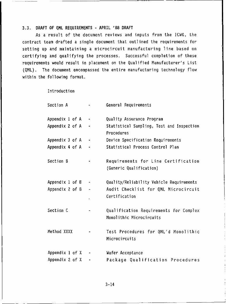
3.3. DRAFT OF QML REQUIREMENTS - APRIL '88 DRAFT
As a result of the document reviews and inputs from the ICWG, the
contract team drafted a single document that outlined the requirements for
setting up and maintaining a microcircuit manufacturing line based on
certifying and qualifying the processes. Successful completion of these
requirements would result in placement on the Qualified Manufacturer's List
(QML). The document encompassed the entire manufacturing technology flow
within the following format.
Introduction
Section A - General Requirements
Appendix 1 of A - Quality Assurance Program
Appendix 2 of A - Statistical Sampling, Test and Inspection
Procedures
Appendix 3 of A - Device Specification Requirements
Appendix 4 of A - Statistical Process Control Plan
Section B - Requirements for Line Certification
(Generic Qualification)
Appendix 1 of B - Quality/Reliability Vehicle Requirements
Appendix 2 of B - Audit Checklist for QML Microcircuit
Certification
Section C Qualification Requirements for Complex
Monolithic Microcircuits
Method XXXX Test Procedures for QML'd Monolithic
Microcircuits
Appendix 1 of X - Wafer Acceptance
Appendix 2 of X - Package Qualification Procedures
3-14
In April of 1988 the first draft of the Generic Qualification document
was released for review and comment. This document followed the outline
given above and was coordinated by RADC/RBRA. The intent was to present QML
implementation requirements for microcircuits to the industry for comment and
critique. The intent of Generic Qualification for QML is to give the
manufacturer needed flexibility and responsibility to control and improve the
high quality and reliability of his product.
The following technical considerations were incorporated into the first
draft document to address the reliability issues of an QML manufacturing
environment:
o Manufacturer's QA Program Plan
o Self Audits
o Technology Review Board (TRB)
o Total Quality Management/Control (TQM/TQC)
o Statistical Process Control (SPC)
o Standard Evaluation Circuit (SEC)
o Quarterly Reports
These key concepts are briefly discussed in the following paragraphs.
3.3.1. Manufacturer's QA Program Plan
The QA Program Plan for QML continues to be the vehicle whereby the
manufacturer maintains control over the quality of his product.
3.3.1.1. QA Program Plan-Section A
As a precondition to qualification, the microcircuit manufacturer shall
establish and implement a quality assurance program. The Quality Assurance
Program Plan shall be submitted to the Qualifying Activity as part of the
certification process.
After a manufacturer receives qualification, he shall not implement any
change in microcircuit design, material, process or control without
concurrent change in the quality assurance program documentation. Changes
3-15

made to the process control or quality control documents listed in the
approved Quality Assurance Program Plan shall be reported to the Qualifying
Activity.
The manufacturer shall be actively developing an SPC program and an
expected date of a full program institution shall be indicated as part of the
Quality Assurance Program plan.
The qualifying activity has the right to remove the QML status of a
line for failure to meet or maintain compliance to any requirements or
failure to meet the Quality Assurance Program Plan submitted as part of
Certification.
The QA Program Plan shall identify minimum loading required to maintain
quality and reliability of the manufacturer's line.
Life Tests shall be performed on the SEC at intervals set by the TRB in
the Quality Assurance Program Plan.
Microcircuits shall be manufactured, processed, and tested in a careful
and workmanlike manner in accordance with good engineering practice, within
the requirements of the QML specification, and within the production
practices, workmanship instructions, inspection and test procedures, and
training aids prepared by the manufacturer in fulfillment of the quality
assurance program.
3.3.1.2. QA Program Plan-Appendix 1 of Section A
As a guide to implementing a QA Program Plan, Appendix 1 of Section A
was included.
The manufacturer's quality assurance program shall demonstrate and
assure that design, mask making, fabrication, assembly, inspection and
testing of microcircuits is adequate to assure compliance with the applicable
requirements and quality standards of the QML document. When any portion of
3-16
the design, fabrication, assembly and testing operation is other than at the
manufacturer's facility, it shall be the responsibility of the manufacturer
to secure and prove the documentation and control of the quality assurance
program of the other location.
All required quality assurance program documentation and records shall
be available for review by the qualifying activity upon request.
The QA Program Plan shall be established and maintained by the
manufacturer, and shall be delivered to the qualifying activity for review
prior to the certification audit. It shall consist of a volume or portfolio,
which will serve to demonstrate to the qualifying activity that the
manufacturer's understanding of a complete quality assurance program, as
exemplified by his documentation system, is adequate to assure compliance
with the applicable specifications and quality standards. If the quality
assurance program exemplified is applied consistently to all product lines
intended to be submitted for acceptance inspection under the QML document,
only one program plan is required for each manufacturing plant; any
difference in treatment of different product lines within a plant shall be
stated and explained in the program plan, or separate program plans prepared
for such different lines. The program plan shall contain, as a minimum,
these items:
o Functional block organizational chart.
o Example of design and manufacturing flow chart.
o Proprietary-document identification.
o Examples of design, material, equipment, visual standard, and
process instructions.
o Examples of records.
o Examples of design, material and process change control documents.
o Examples of failure and defect analysis and feedback documents.
o Examples of corrective arction and evaluation documents.
o Manufacturer's internal instructions for internal visual
inspection.
3-17

o Examples of test travelers.
o Examples of design and construction baseline.
o Manufacturer's self audit program (see paragraph 30 herein).
3.3.1.3. QA Program Plan-Section B
The manufacturer shall provide documentation showing evidence that
their Quality Assurance Program Plan has been implemented.
3.3.2. Self Audit
The manufacturer's self audit is an ongoing discipline that serves to
maintain manufacturing quality by reviewing, improving and checking the
manufacturers procedures for compliance to the QA Plan.
3.3.2.1. Self Audit-Section A
The manufacturer's self audit not only helps maintain manufacturing
quality but the self audit results are submitted to the qualifying activity
at the time of certification as one of the means of certifying that all
facilities, equipment, procedures, analytical tools, and documentation are
appropriate for the manufacture of high quality, reliable, monolithic
microcircuits.
3.3.2.2. Self Audit-Appendix 1 of Section A
The intent of a self-audit program is to assure continued conformance
to this QML specification and provide the qualifying activity a means of
having precertification audit data.
The manufacturer shall establish an irdependent self-audit program
under the direction of the TRB to assess the effectiveness of the
manufacturer's compliance to all applicable specifications. The
manufacturer's self-audit program which identifies key review areas, their
frequency of audit, and the corrective action system to be employed when
variatiori from the apprcved procedures or specification requirements are
identified shall be included in the program plan. The self-audit program
shall as a minimum incorporate the following requirements:
3-18

o A system to identify and correct any deficiencies (e.g. design,
processing and testing) or deviations from the QA Program Plan.
o Provide for review of all deviations from critical documents such
as baseline(s), flow chart(s), means of traceability, QCI
procedures when applicable.
o Specify the selection and training/retraining requirements for
auditors.
0 Specify the self-audit frequencies and require that a schedule be
established and adhered to.
The designated auditors shall be independent from the area being
audited. If the use of an independent auditor is not practical, then as a
minimum another individual should be assigned to participate in the audit or
review the results with the auditor from the area. The auditors shall be
familiar with the area to be audited, with the applicable QA Plan, and
provided with an appropriate checklist for annotating deficiencies. Prior to
the audit, the assigned auditor(s) shall review the previous audit checklist
to assure corrective actions have been implemented and are sufficient to
correct the deficiencies.
The self-audit checklist shall be approved by the TRB and maintained
under document control. The checklist shall assure that the quality
assurance system is adequate and followed by all personnel in each area.
3.3.3. Technology Review Board (TRB)
The TRB is the board appointed by the manufacturer, made up of
representatives of each function in the manufacturing line, responsible for
acquiring, maintaining, and reporting the status of the line to the
3-19

3.3.3.1. Technology Review Board-Section A
The organizational structure of the TRB shall be up to the manufacturer
but the manufacturer shall submit the n',nes, addresses, and phone numbers of
the members of the TRB to the Qualifying Activity including a list of contact
people. Any changes to the TRB shall be included in the quarterly report. Any
change in the contact person or persons shall be reported to the Qualifying
Activity immediately. Records shall be maintained of the TRB's membership,
deliberations and decisions. Records shall also be kept of dissenting
opinions of board members.
The TRB shall submit quarterly to the Qualifying Activity a Quarterly
Status Report.
The manufacturer's Technology Review Board will judge the current
status of the QA Program Plan and reliability of its microcircuits by review
of the SPC and TQC status of the manufacturer's line, reliability test data
(i.e., PM, TCV, SEC and device), the rate of board assembly failures and
field returns, and the Failure Analysis (FA) results of screen and burn-in
failures.
The frequency and testing methods for interim evaluations of the SEC
and/or the TCV are to be determined by the TRB based on the manufacturer's
assessment of risk. The manufacturer's interim SEC and TCV evaluation plan
shall be documented.
When reliability of shipped microcircuits is called into question, the
TRB shall provide quick evaluation and/or corrective action and prompt
notification to the Qualifying Activity to preserve the manufacturer's
qualified status.
All changes to any part of a QML'd manufacturers line are to be
monitored (ruL necessarily formally approved) by the manufacturer's TRB,
accompanied by changes in the Quality Assurance Program Plan when applicable,
and available to the Qualifying Activity. In addition when applicable,
3-20

changes shall be documented as to the reason for the change with supporting
data taken to support the change, including reliability data.
The decision as to the criticality of the change shall be guided by the
potential effect of the change on quality, reliability, performance and
interchangeability of the resulting microcircuits. For any change that
merits consideration for requalification the TRB shall decide if
requalification is needed. Microcircuits shall be shipped following a change
only upon approval of the TRB following the review of data available to show
that the change produces the required quality and reliable microcircuits.
The TRB shall maintain a Technology Characterization Vehicle (TCV) to
be complete and accurate for all known intrinsic reliability failure
mechanisms and report such status in the Quarterly Status Report.
Sampling for nonelectrical screens can be an acceptable substitute for
any specified screening procedure provided that the sampling procedure and
supporting data be documented and approved by the TRB and submitted to the
Qualifying Activity.
A TRB representative shall verify screening, qualification and QCI
records when corrective addenda affect lot jeopardy.
All self-audit reports will be filed and maintained by the TRB. The
TRB shall establish a procedure to follow up on all audit deficiencies to
assure that the corrective actions have been implemented in a timely manner.
The self-audit frequency shall be established with a schedule by the
TRB but in no case exceed one year for each area, unless authorized by the
Qualifying Activity.
The InanuFdcturer shall" deonstrate Ce process capabilit'y f tho
following areas of design:
o Design simulation versus routing simulation
3-21

o CAD routing and post-routing simulation
o Design check software verification
o Testability/fault coverage
Test plans for each oF these areas shall be approved by the TRB and
submitted as part of the Certification Test Plan. All tests shall be
completed and documented before certification is granted.
The TRB shall determine the tests to be accomplished on the TCV, SEC,
and PM and submit to the Qualifying Activity a test plan with parametric
limits and accept/reject criteria. All elements in the database shall be in
compliance with the geometric and electrical design rules approved by the
TRB. Documented design rules consisting of geometric layout and electrical
rules for wafer fabrication, approved by the TRB and implemented in the
design of all QML microcircuits shall be documented and verified. The
manufacturer shall control the environment of the QML wafer fabrication
facility in terms of relative humidity, temperature, and particle count as
specified by the TRB. The Qualifying Activity shall be shown evidence that
each processed wafer in a wafer fabrication facility contains parametric
monitors that include the parameter requirements specified and meet the
pass/fail criteria for each parametric structure established by the TRB.
Wire bond materials and equipment calibration, automatiu and/or manual, shall
meet the reliability criteria established by the TRB and approved by the
Qualifying Activity. Tape-automated-bonding (TAB) materials and equipment
shall meet the reliability criteria established by the TRB. The Qualifying
Activity shall clearly identify the deficiency in the Audit Exit Report and
obtain TRB signature verifying notification.
After the initial QML qualification process, the SEC shall be
manufactured at least every 12 months, or more often as determined by the
TRB. After initial certification/qualificatio. the TCV shall be manufactured
and tested at least every 12 months, or more often as determined by the TRB.
3-22

3.3.4. Total Quality Manaqement/Control (TQM/TQC)
QML manufacturers shall maintain a system of Total Quality Control
(TQC) intended to continuously improve the quality and reliability of the
microcircuits produced .
3.3.4.1. Total Quality Management/Control (TQM/TQC)-Appendix 1 of Section A
A company-wide toL.., quality control (TQC) policy shall be adopted to
describe top management's commitment to quality assurance. Quality assurance
objectives shall be established for quality elements such as field
performance and reliability levels, internal inspection quality standards,
supplier quality assessment and personnel training/qualification.
Documentation is required on the wafer fabrication process including
the SPC and TQC p igrams.
3.3.5. Statistical Process Control-Section A
The manufacturer shall be actively developing an SPC program and shall
describe and indicate in the Quality Assurance Program Plan the goals of the
program. Failure to meet these goals can be grounds for removal from QML.
The status of the SPC programs shall be reported quarterly in the status
reports issued by the TRB.
3.3.5.1. Statistical Process Control-Appendix 1 of Section A
The SPC program shall be documented and the means for collecting,
recording and interpreting the data shall be described. Also, SPC training
programs shall be discussed.
3.3.5.2. Statistical Process Control-Section B
The manufacturer shall provide documentation and records, upon request,
to the qualifying activity that criticdl nodes are under SPC or other
in-process monitoring programs. Implementation dates for areas not under SPC
shall be provided. For exampie, the PM medSur-eme Ls Sildill be used dS part o'
the manufacturer's SPC program.
3-23
3.3.6. Standard Evaluation Circuit (SEC)-Section A
The manufacturer's Technology Review Board will judge the current
status of the quality and reliability of its microcircuits by review of the
SPC and TQC status of the manufacturer's line, reliability test data (i.e.,
PM, TCV, SEC and device), the rate of board assembly failures and field
returns, and the Failure Analysis (FA) results of burn-in failures and board
assembly and field returns. The SEC is a key test vehicle in assessing the
reliability characteristics of the technology.
3.3.6.1. Standard Evaluation Circuit (SEC)-Section A
The wafer fabrication process shall be monitored and controlled using a
Standard Evaluation Circuit (SEC), Technology Characterization Vehicle (TCV)
and Parametric Monitors (PM). The frequency and testing methods for interim
evaluations of the SEC and/or the TCV are to be determined by the TRB based
on the manufacturer's assessment of risk. The SEC and TCV data is to be used
as a tool for monitoring the quality and reliability of the manufacturer's
line and does not automatically disqualify a manufacturer when trends or
limits require corrective action.
A summary of reliability test data, including SEC data, collected over
the past quarter shall be included in the Quarterly Status Report. The
results shall be compared with the current approved baseline data. If, at
any time, there is a shortage of QML microcircuit designs available for
manufacture on the QML'd line, the SEC and PM shall be continuously produced
and tested along with Non-QML microcircuit designs.
A QML manufacturer shall process, screen and life test an SEC at
intervals set by the TRB in the Quality Assurance Program Plan.
3.3.6.2. Standard Evaluation Circuit (SEC)-Appendix 1 of Section A
Documentation is required on the SEC design, including the
functionality, its performance limits, and all documentation required for
standard design qualification per the TRB.
3-24

3.3.6.3. Standard Evaluation Circuit (SEC) Section B
The SEC design and construction baseline form (i.e., DESC EQM-42) shall
be included in the manufacturers program plan and maintained under document
control. A manufacturer shall have a Standard Evaluation Circuit (SEC) for
each technology to be certified. The SEC may be designed solely for its role
as a qualification and reliability monitoring vehicle or it may be a product
meant for system use.
For initial certification, a sufficient number of SEC devices randomly
chosen and evenly distributed from wafers from three homogeneous wafer lots
passing PM tests and screened in the technology to be qualified at the
fabrication facility to be qualified shall be evaluated for surrogate
feasibility. The number of SEC device failures will serve as a qualification
benchmark for the technology. Failure Analysis (FA) shall be done on all
failed parts and action taken to correct any problems found. The SEC
reliability data, including failure analysis results, shall be available for
review by the Qualifying Activity.
The TRB shall determine the tests to be accomplished on the TCV, SEC,
and PM and submit to the Qualifying Activity a test plan with parametric
limits and accept/reject criteria.
The manufacturer shall demonstrate the capability of the assembly and
package processes by qualifying the package to be used to house the SEC chip.
The test results of the SEC package qualification shall be submitted to the
Qualifying Activity as part of the Certification procedure.
3.3.6.4. Standard Evaluation Circuit (SEC)-Appendix I of Section B
The Standard Evaluation Circuit (SEC) shall, as a minimum, monitor the
long term reliability parameters of the wafer fabrication facility.
When radiation hardness is a requirement of the technology, the SEC
shall be used to certify, qualify, and monitor the radiation hardness of a
specific fabrication technology in a specific fabrication facility. The SEC
3-25

shall be designed so it can be used to assess and monitor the radiation
hardness of the technology
3.3.7. Quarterly Report
A Quarterly report is to be issued by the manufacturer's TRB to the
Qualifying Activity summarizing all reliability and quality testing results,
explaining all modifications to the manufacturing line since last reporting
period, and detailing the disposition of all microcircuits affected by any
changes or corrective actions to the process.
3.3.7.1. Quarterly Report-Section A
As part of the quarterly status report the TRB should include a summary
of results of any catastrophic failures (i.e., shorts or opens measurable or
detectable at 250C) subsequent to burn-in which were analyzed.
3.3.7.2. Quarterly Report-Appendix I of Section A
The manufacturer shall submit to the Qualifying Activity in the
Quarterly Reports, any deficiencies and corrective actions. The Qualifying
Activity may modify the frequency of the self-audit or require additional
testing based on the data from the self-audit.
3.4. SUMMARY
The investigation task culminated with the issuance of the 8 Apr 1988
draft document. This document included inputs from the contract team and the
Industry Coordinating Working Group (ICWG). In an attempt to include
requirements and standards in a single document, a multi-section document was
drafted. Section A identified General Requirements; section B included Line
Certification Requirements; and section C was Qualification Requirements.
Each section included appendices. Section A Appendix I was Quality Assurance
Program requirements, Appendix 2 was Statistical Process Control Plan
re....r..ent., .. .Ap.endi 3" OSpecification requirements ad Aendix 4
was Statistical Process Control requirements. Section B Appendix 1 was
Quality/Reliability Vehicle requirements and Appendix 2 was Audit Checklist
3-26

for QML Microcircuit Certification requirements. The final section to the 8
April 1988 draft document was "Method XXXX" which included all testing
requirements for qualification and screening.
Key elements that developed during this phase were, Total Quality
Management, Technology Review Board, Standard Evaluation CircLit, Parametric
Monitor, Technology Control Vehicle, and QML Plan. The goal in establishing
this generic qualification procedure document, was to identify those controls
and measurements that made sense to industry and DoD without restricting the
ability of integrated circuit manufacturers to improve and maintain highly
reliable and quality products.
The activity of the investigation task was reported in an interim
report and orally at the VHSIC/VLSI Qualification, Reliability and Logistics
Workshop, September 1988, in Scottsdale, Arizona.
The draft procedures underwent an extensive review during the next year
and from that review the following Generic Qualification Flow Diagram shown
in Figure 1 emerged.
3-27

GENERIC QUALIFICATION
FLOW DIAGRAMQUALITY MANAGEMENT PROGRAM! FIGURE-1
II
FDGSRG-,
CERTIFICATION REQUIREMENTS CAPABILITY E G SIMULATION
ADDRE NCSS I E.G. SEC/TCV/PMj
NLDPACKAGE &ASSEMBLY
SSATISFACTORY
... _.._.QUALIFICATION REQUIREMENTS
NM ORTCNLG
IDEVICE SPECIFICATION UNDER / CONFORMANCE , PROBEM
PRODUCT BUILD REQUIREMENTS(INCLUDES PACKAGE)
iSCREENS
MARKING SHIP/INSERT OML PRODUCT
3-28

4. TASK III - DEMONSTRATION AND GENERAL SUPPORT
4.1. INTRODUCTION
For Task III the contract team was required to demonstrate the proposed
QML procedures by implementing them on their own VHSIC/VLSI process lines.
To accomplish this task alpha sites at GE and AT&T were chosen. In addition
to these alpha site demonstrations the contract team would also provide
support for beta site demonstrations which would be conducted by companies
solicited from the VLSI community at large. The contract team also
accumulated a large set of data on state-of-the-art VLSI equipment, software,
and techniques for use in preparation of a handbook which could be made
available to the industry.
Both GE and AT&T used draft versions of MIL-I-38535 (the QML
requirements document). Some differences in requirements occurred as the
document and team understanding matured.
4.2. ALPHA SITE DEMONSTRATIONS
The GE alpha site consisted of the GE design center at Utica, NY. The
technology in use was a 1.25 micron CMOS standard cell process which was
fabricated, assembled and tested at GE Microelectronics Center (GE-MEC) in
Research Triangle Park, NC. GE planned to demonstrate three chips with a
complexity of 6,000, 21,000, and 28,000 gates respectively, plus an SEC
containing 10,000 gates.
The QML alpha site for AT&T in Allentown, PA involved their Bell
Laboratory Design Center, AT&T-ME Mask Facility, MOS V CMOS Clean Room, and
the "Just-in-Time" (JIT) Ceramic Assembly and Test Area. A standard
evaluation circuit, a technology evaluation vehicle, and three production
devices were fabricated in order to demonstrate the generic qualification
principle. AT&T formed a TRB which submitted a quality plan in July of 1988
to start the formal process of qualification.
4-1

4.2.1. Alpha Site Validation
The certification phase of generic qualification involves a process of
validation of the manufacturers capability. The validation process has two
parts. In the first part the manufacturer submits documentation to DESC/RADC
on his quality programs and process capabilities. After evaluation of the
submitted documentation DESC/RADC performs an on-site validation review to
provide a final assessment of the manufacturers readiness.
In order to demonstrate the effectiveness of the requirements
documented in the draft MIL-I-38535 specification, RADC performed two
practice QML validations at the Contractor sites. The first validation
demonstration was a full fledged validation of the entire technology flow at
AT&T's Allentown, PA facility in November of 1988. The second demonstration
concentrated on GE's Design Center located in Utica, NY and was performed in
February of 1989.
4.2.1.1. Pre Validation Submittal
In preparation of the trial validation review conducted by Government
representatives from RADC and DESC, both AT&T and GE prepared Quality
Assurance Program Plans (later called Quality Management Plan) and submitted
them to RADC and DESC before the actual validation. In AT&T's case the
Quality Assurance Program plan detailed AT&T's proposed QML technology from
design through test. GE's plan concentrated on design only. The following
paragraphs summarize the actual review conducted at AT&T and GE.
4.2.1.2. Validation Reviews
A validation team consisting of ten representatives from RADC and DESC
performed a certification validation audit at AT&T Allentown PA's facilities
on 15-18 of November 1988. The purpose of this demonstration was to test out
the concepts associated with a QML validation and make changes to the
requirements and procedures based on the outcome.
The first day of the trial validation was an intense review of AT&T's
Quality program and proposed technology flow. Present from AT&T was
management and the Technology Review Board. Discussions and questions
4-2

concentrated on AT&T's business plans for the technology, marketing plans,
quality management approach (including TQM), technology review board
operation and effectiveness, SPC program including goals and monitoring
program and change control program. On the technical side discussions
centered on contamination control, SEC design and effectiveness, TCV program,
and ESD policy. At the end of the meeting RADC and DESC gave AT&T an
outbriefing of their findings.
The next three days were spent with RADC and DESC touring the
facilities and spot checking various operations. A full day was spent with
the design group where questions centered on how AT&T developed and verified
their models used in simulation; and checking designs. AT&T presented detail
information on how various design, electrical and reliability rules were
established, verified and checked. Tours and audits of AT&T fabrication
line, JIT assembly line and test areas were conducted on subsequent days. At
the end of each day RADC and DESC gave an outbriefing of their findings.
On the final day, a formal outbriefing was given to AT&T management and
TRB. Also, AT&T gave RADC and DESC an outbriefing on how they could better
organize and perform an audit function. Generally, the validation was an
informative exchange of issues related to reliability, quality, management
and environmental concerns. Suggestions for improvements included better
definition of what should be submitted to the validation team in the Quality
Assurance Program plan, smaller audit teams during the facility tours and
better organization of questioning during the Design Center Review.
At GE, review of their design center was conducted on I Feb 1989. The
initial QML validation review was to consist of a review of GE/Utica design
and GE/RTP fabrication, assembly and test portions. Only the GE/Utica review
was conducted. The following is a summary of the review at GE/Utica.
The Manager of Engineering at GE/Utica presented an Organizational
Chart for GE Aerospace down to the ASIC Design Unit level. The manager of
ASIC Design, provided a brief summary of the AVLSI 1.25 micron technology and
4-3

reviewed the Technology Review Board (TRB) function at GE/Utica and the
interface with the GE/RTP TRB.
GE/Utica encouraged the RADC representatives to be open and frank with
any issues that were to be addressed during the validation review. At that
time RADC presented an overview of the Qualification Procedures activity to
date and the intent of the Validation Review.
During the remaining portion of the Validation Review question and
answers were exchanged between RADC and GE representative.
o GE/Utica ASIC Design function deals mainly with internal system
requirements and an informal hand-off is made from systems
engineering. For QML validation, a documented and 1RB approved
hand-off of system requirements is required.
o Since GE/Utica interfaced with GE/RTP for fabrication, design
rules and cell library maintenance was handled by GE/RTP. A
documented interface between GE/Utica and GE/RTP was required for
the validation review. The interface process was electronic but
not well documented. GE/Utica's position that GE/RTP would
present that documentation during a subsequent validation at
GE/RTP still did not demonstrate an "in place" system. Interface
responsibility must be shared between design and fabrication
functions and validated by both functions.
0 GE/Utica does not have behavioral models but does have structural
models which could be converted into VHDL structural models with
an implemented translator. GE/Utica is actively pursuing VHDL in
the future development of ASIC design. Designer training and VHDL
implementation in future CAD tools is part of the on-going effort
at GE/Utica. Review of MIL-STD-454, requirement 64, was needpd to
better understand the VHDL requirement.
4-4

4.3. BETA SITE DEMONSTRATIONS
A number of companies, in addition to the alpha site companies, were
invited by DOD to participate in the refinement of MIL-I-38535 prior to its
formal release. These volunteer participants were helpful in the
coordination of the requirements. The beta site companies would be among the
first manufacturers to be formally audited to the Qualified Manufacturer's
List (QML) requirements defined in MIL-I-38535.
4.3.1. Companies Involved in Beta Sites
Eight companies accepted the beta site invitations and plan to
demonstrate compliance to the requirements of MIL-I-38535. These were:
GE Solid State Findley OH
Harris Semiconductor Melbourne FL
Intel Chandler AZ
National Semiconductor Sunnyvale CA
Texas Instruments Dallas TX
VLSI Technologies San Jose CA
LSI Logics Milpitas CA
IBM Manassas VA
Since the beta site commitments have been made, GE Solid State at
Findley and GE-MEC have been purchased by Harris Semiconductor, making some
alpha and beta site schedules in question. Also, Honeywell in Plymouth, MN
was added as beta site.
4.3.2. Progress
Most of the beta sites plan to obtain QML status by end of 1990. Final
release of MIL-I-38535 is expected by the end of 1989.
4.4. BETA SITE MEETINGS
Throughout the beta site process a series of meetings was held between
all beta site companies, DOD representatives, and the alpha site companies to
discuss major issues of preliminary versions of MIL-I-38535. Each meeting
concentrated on a specific topic related to QML; such as fabrication,
design/test, assembly/packaging, screens/QCI/Qualification and Radiation
Hardness/Space Quality.
4-5

The results of these meetings were integrated in subsequent drafts of
MIL-I-38535. A final review of MIL-I-38535 was released for formal
coordination in Fall 1989.
4.5. GENERAL SUPPORT
4.5.1. Handbook
As part of the contract a guideline handbook to help the manufacturer
in implementation of built-in quality and reliability was developed.
Material for the handbook was solicited from equipment manufacturer and
software vendors throughout the microelectronics industry. Nearly 150 data
sheets were received in response to this solicitation. The contract team
formatted some of the information into handbook form using the format shown
in Figure 2. The sample handbook needs to be further expanded to improve its
usefulness.
4.5.2. Proposed Test Methods
During the review of existing military documents, several new test
methods were identified as necessary to completely test digital devices.
There proposed test methods are found in Appendix II and are presently being
evaluated by industry and DoD for consideration for inclusion into
Mil-Std-883.
4-6

VOLUME: FABRICATION HANDBOOK # 2.A.6
ISSUE DATE: 7/13/89 REVIEW CYCLE: 12 Mo. REVIEW DATE:
CATEGORY: EQUIPMENT
IDENTIFICATION: SAMCO PDM-303
APPLICATION: PLASMA CVD MULTI-CHAMBER
DESCRIPTION/COST:
This is a multi-chamber reactor for depositing multi-layer amorphous silicon films with each deposited in
individual chamber, dual rack mounted units (1710 x 55 x 1050 and 1730 x 1030 x 1050) and a separate RF
power control unit. The reactor has fine sample holders with rotating mark plate. There are three
independent reaction (p, n. and i) chambers with a fourth "loading chamber", all enclosed in safe enclosure
The main unit has easy access gas inlets and outlets and a built-in vacuum system with its own
vacuum/pressure gauges and gas flow meters.
SAMCO indicates that prices start at $25,000 and range up to about $100,000 for a single chamber system,
depending on application and options.
DOCUMENTATION/SUPPORT:
OPTO FILMS, a research laboratory in the United States for SAMCO, provides after sales service, applications
advice, user's manuals, installation assistance, and training.
USERS:
A list of customers is available to potential customers on a case by case basis. The list includes many
well-known companies and universities in the United States and Japan.
USERS:
COMPANY/CONTACT:
Japan: SAMCO International Inc. Phone (075) 621-7841
33 Tanakamiya-cho, Takeda, Fushimi-ku Fax # (075) 621-0936
KYOTO 612 JAPAN Telex 5422664 SAMCO-J
USA: Opto Films
532 Wedell Drive, Ste. 5 Phone (4)8) 734-0459
Sunnyvale, CA 94089 Fax # (408) 734-0961 Figure 24-7

VOLUME: FABRICATION HANDBOOK # 2.A.6
TECHNICAL DATA:
Electrode: Parallel place
Reactor: 3 chambers (*2 or 4 chambers), pyrex made (*quartz or stainless steel)
Substrate: Max 3500C, 160 rm , each unit can be heated
Gas control: Mechanical flow meter (3 units)
RF power supply: 13.55 M z, 150 W or *400 W
Sample preparation chamnbr: Stainless made
Vacuum lii.e: Reactor - oil diffusion pump, PC - rotary pump
Vacuum gauge: Thermocouple gauge, capacitance manometer, ionization gauge
Optional Accessories:
o Mass flow controller (in case of adding more than 3 components)
o Plasma radiation monitor (wave length 200-800 rn)
o Gas scrubber unit (for SiH4, PH3 and B2H6)
o Toxic gas monitoL !PH3, AsH3, H1S and etc.)
o Computer controller
FEATURES:
o Deposition of multi-layer amorphous silicon films with each layer deposited in an independent chamber
(example: p, i, n layers)
o Multi-step plasma etching and stripping of semiconductor products
o Deposition, sputtering, or vacu-m evaporation can also be incorporated into the total process using a
single multi-chamber system.
Figure 2. Cont'd
4-8

5. CONCLUSIONS AND RECOMMENDATIONS
5.1. CONCLUSIONS
Generic qualification of the manufacture of VHSIC/VLSI microcircuits is
a concept whose time has come. From the beginning of the contract, until its
completion, the importance of quality management and the need for a "living"
document have reverberated throughout industry. The concept of "building in"
quality by characterizing and controlling the process was readily agreed upon
by both the contract team and the customer. Releases from DoD during the
contract period further supported a commitment to total quality management
and streamlining the procurement policies within the DoD. With a clear
objective set, the real challenge was to provide a well documented policy for
the DoD which provided industry a clear concise method for qualifying a
manufacturing process from design through final procurement by the DoD.
Highlights of how the resulting qualification procedures for VHSIC/VLSI met
the goals of the contract are give in the areas of design, fabrication,
assembly and test.
5.1.1. Design
The design community is well equipped with CAE and CAD toolF to provide
verified designs and test criteria to the fabrication, assembly and test
processes. The new procedures stress the need of design to interface and
maintain ongoing concurrence with these processes. A design methodology may
be qualified under the new procedures by including the design function in the
manufacturer's overall quality management plan. Although design tools
themselves are not qualified, they become part of a qualified process,
showing a well documented design flow ana control of all steps and tools used
within the flow.
5.1.2. Fabrication
Previously qualification of DoD procured microcircuits was only done
through qualification testing of parts that were fabricated on a certified
line. For generic qualification, the fabrication processes are now able to
be qualified with a well documented quality management plan guaranteeing
built in quality and reliability. With well defined fabrication processes
5-1

using tools such as statistical process control and standard evaluation
circuits, the manufacturer's fabrication process can be qualified in
conjunction with its approved quality plan. Both high volume and low volume
designs benefit with only surrogate devices required for qualification
testing. The new qualification document encourages constant improvement in
quality and reliability with quarterly status reports to the qualifying
activity notifying them of qualification status and proposed changes for
improvement.
5.1.3. Assembly and Packaging
Generic qualification of the assembly manufacturing process ensures
that quality and reliability is maintained through continuous control of the
assembly process flow. Once the quality management plan is in place to show
that characterization of the assembly process has been completed and the
processes are well documented and under control, the qualifying activity can
validate that the assembly process is ready for line qualification. Once the
assembly processes are qualified, process monitoring and in-line testing
replaces end-of-process testing. The manufacturer uses his own quality
management plan to establish the criteria which ensures quality and
reliability in the finished product.
Packaging of microcircuits under generic qualification is also enhanced
by allowing minimal need to perform qualification testing of parts due to
packaging variations. The packages used for generic qualification can be
qualified by package technology styles. When new packages are added to the
package technology, only those portions of the characterization testing
affected need qualification.
5.1.4. Test
Under generic qualification all phases of screens, and technology
conformance inspections (TCI) are integrated from design to final test and
shipping of microcircuits. Automatic test equipment is identified, and the
design function must design in testability, validate the design through
simulations and then provide test vectors to screen finished product.
Generic qualification also requires documented interfaces between design,
5-2

fabrication, assembly and test to ensure first-pass success on designs at the
screening and TCI steps. Reliability and quality requirements are built-in
throughout the manufacturing cycle as identified in the manufacturer's
quality management plan. ESD protection, electromigration concerns and other
reliability issues are addressed prior to the beginning of the design.
5.2. RECOMMENDATIONS
Generic qualification has provided the means to qualify the manufacture
of microcircuits for many of today's DoD needs based on well established
criteria such as temperature, electrical and mechanical stress. There is a
need to add radiation and space environment stresses to generic qualification
capability if all microcircuit applications are to be totally addressed.
Additional modeling and test structures should be developed to enhance
generic qualification to eliminate end of process testing that is still
required for these applications.
The use of multiple design sites for a given technology should be
included in generic qualification to give flexibility to those environments
where the front-end design is not an integral part of the fabrication,
assembly and test functions. Integration of quality management at remote
design sites must be addressed to identify requirements for generic
qualification.
Package qualification needs to address off-shore and on-shore issues.
The more integrated the quality management plan is the better generic
qualification is designed to work. Therefore, as in multiple design sites,
there is a need to define an acceptable interface at the Technology Review
Board (TRB) level between all phases of microcircuit manufacture.
In addition to the generic qualification document, the guidelines
document which was started should be further developed to provide a means of
informing the microcircuit industry of on going improvements in microcircuit
technologies. Both processes and equipment should be included that would
further enhance microcircuit quality and reliability.
5-3

Appendix A
General Specification for
Integrated Circuits (Microcircuits)
Manufacturing

INCH-POUND
MIL-1-3853518 December 1989
MILITARY SPECIFICATION
INTEGRATED CIRCUITS (MICROCIRCUITS) MANUFACTURING,
GENERAL SPECIFICATION FOR
This specification is approved for use by all Depart-ments and Agencies of the Department of Defense.
This specification is intended to support Government microcircuit appLica-tion and logistic prog-rams. Detailed characteristics of microcircuitsneeded for a program are to be defined by detail drawings or specifications.
1. SCOPE
1.1 Scope. This specification establishes the general requirements for integratedcircuits or microcircuits and the quality and reliability assurance requirementswhich must be met for their acquisition. Detail requirements, specificcharacteristics of microcircuits, and other provisions which are sensitive to theparticular use intended shall be specified in the device procurement specification.Quality assurance requirements outlined herein are for all microcircuits built on amanufacturing line which is controlled through a manufacturer's quality management(OM) program and has been certified and qualified in accordance with requirementsherein. The manufacturing line shall be a stable process flow for allmicrocircuits. A single level of product assurance (including Radiation HardnessAssurance (RHA)) is provided for :n zhis specification. The certification andqualification sections found herein outline the requirements to be met by amanufacturer to be listed on a Qualified Manufacturer Listing (QML). After listingof a technology flow on a QML, the manufacturer must continually meet or improve theestablished baseline of certified and qualified procedures, the quality management(OM) program, the technology review board (TRB), the status reporting and quality andreliability assurance requirements for all QML products. This specification alsodefines the tests which must be performed on each product built. NOTE: Thisspecification requires a manufacturer to establish a baseline. As the technologymatures and reliability and quality data are gathered, the manufacturer through thequality management (OM) program and the technology review board (TRB) may modify,substitute or delete tests. Notification of such actions shall be detailed in thestatus reports submitted to the qualifying activity.
2. APPLICABLE DOCUMENTS
2.1 Government documents.
2.1.1 Specifications, standards and handbooks. The following specifications,standards, and handbooks form a part of this document to the extent specifiedherein. Unless otherwise specified, the issues of these documents are those listedin the issue of the Department of Defense Index of Specifications and Standards(DODISS) and supplement thereto, cited in the solicitation.
SPECIFICATIONS
MILITARY
MIL-M-55565 Microcircuits, Packaging of.
BeneticIat comments (recommencations, aacitions, oeLetions) and any perLinc.t data,which may be of use in improving this document should be addressed to: Rome AirDevelopment Center (RBE-2), Griffiss AFB. NY 13441, by using the self-addressedStandardization Document Improvement Prs:osat (DD Form 1426) appearing at the endof this document or by letter.
AMSC N/A FSC 5962DISTRIBUTION STATEMENT A. Approved for public release; distribution is unlimited.
A-i

MIL-1-38535
STANDARDS
NI LI TARY
MIL-STD-100 " Engineering Drawing Practices.NIL-STD-129 - Marking for Shipment and Storage.MIL-STD-883 Test Methods and Procedures for Microelectronics.MIL-STD-1331 Parameters to be Controlled for the Specification of
Microcircuits.MIL-STD-1285 - Marking of ELectrical and Electronic parts.MIL-STD-1686 Electrostatic Discharge Control Program for Protection of
Electrical and Electronic Parts, Assemblies and Equipment(Excluding Electrically Initiated Explosive Devices).
HANDBOOKS
NILITARY
NIL-HDBK-263 Electrostatic Discharge Control Handbook for Protectionof Electrical and Electronic Parts. Assemblies andEquipment (Excluding Electrically Initiated ExplosiveDevices).
Unless otherwise indicated, copies of federal and military specifications,standards, and handbooks are available from the Naval Publications and Forms Center,(ATTN: NPODS), 5801 Tabor Avenue, Philadelphia, PA 19120-5099, or telephone (215)697-2179.)
2.1.2 Other Government documents, drawings, and publications. The following otherGovernment documents, drawings, and publications form a part of this document to theextent specified herein. Unless otherwise specified, the issues are those cited ineffect on the date of the solicitation.
Handbook H4/H8 Commercial and Government Entity (CAGE) Handbook.DESC-EQN-42 Baseline Sheet for JAN Microcircuits.NAVSHIPS 0967-190-4010 Manufacturer's Designating Symbols.
(Copies of other Government documents required by contractors in connection withspecific acquisition functions should be obtained from the contracting activity or asdirected by the contracting activity.)
2.2 Non-Government publications. The following documents form a part of thisdocument to the extent specified herein. Unless otherwise specified, the issues ofthe documents which are DOD adopted are those Listed in the issue of the DODISS citedin the solicitation. Unless otherwise specified, the issues of documents not Listedin the DODISS are the issues of the documents cited in the solicitation.
ELECTRONIC INDUSTRIES ASSOCIATION (EIA)
EIA-STD-RS-471 Symbol and Label for Electrostatic Sensitive Devices.JEDEC Publication 19 - General Standard for Statistical Process Control.
JEDEC Publication 108 - Distributor Requirements for Handling ElectrostaticDischarge Sensitive (ESDS) Devices.
JEDEC Publication 109 - General Requirements For Distributors of militaryIntegrated Circuits.
(Application for copies should be addressed to the Electronic IndustriesAbociation, 200i Eye street, N.W., Washington, DC 20006.)
A-2

MIL-1-38535
NATIONAL INSTITUTE OF STANDARDS AND TECHNOLOGY
Malcolm Batdridge National Quality Award.
(Application for copies should be addressed to Malcolm BaLdridge NationalQuality Award, National Institute of Standards and Technology, Gaithersburg, MD20899.)
(Non-Government standards and other publications are normally available fromthe organizations that prepare or distribute the documents. These documentsalso may be available in or through libraries or other informational services.)
2.3 Order of precedence. In the event of conflict between the text of thisspecification and the references cited herein (except for device procurementspecifications), the text of this specification shall take precedence. Nothing inthis specificaton, however, shall supersede applicable Laws and regulations unless aspecific exemption has been obtained.
3. REQUIREMENTS
3.1 General. The manufacturer of microcircuits in compliance with thisspecification shall have and use production and test facilities and a qualitymanagement (QM) program to assure successful compliance with the provisions of thisspecification.
3.1.1 Reference to applicable device procurement specification. For purposes ofthis specification, when the term "as specified" is used without additional referenceto a specific location or document, the intended reference shall be to the deviceprocurement specification.
3.1.2 Conflicting requirements. In the event of a conflict between therequirements of this specification and other requirements of the device procurementspecification, the precedence in which requirements shall govern, in descendingorder, is as follows:
a. Applicable device procurement specification.
b. This specification.
c. Specifications, standards, and other documents referenced in 2.1.
3.2 Item requirements. The individual item requirements for integrated circuitsdelivered under this specification shall be documented in the device procurementspecification prepared in accordance with 3.6 herein. Unless otherwise specified,all devices produced under this specification shall have a temperature range of -55*Cto +125°C. However, the standard evaluation circuit (SEC) shall be documented on adevice procurement specification and shall have an operating temperature (case orambient, as specified) range from -55"C to +125°C and any references to minimum ormaximum operating temperatures shall refer to the respective lower and upper limitsof this range. NOTE: If any of the provisions of this document are violated or notmet, total compliance cannot be claimed to this document and devices cannot beprovided as OML devices.
3.2.1 Country of manufacture. All QML microcircuits shall be manufactured,assembled, and tested within the United States and its territories except as providedby international agreement establishing reciprocal and equivalent government qualitycontrol systems and procedures.
A-3

MIL-1-38535
3.3 Ciasification of requirements. The requirements of the microcircuits areclassified in the generic qualification flow diagram (see figure 1).
3.3.1 Certification of conformance and acquisition traceability. Manufacturers orsuppliers including distributors who offer QML microcircuits described by thisspecification shall provide written certification, signed by the corporate officerwho hes management responsibility for the production of the OML microcircuits, (1)that the OML microcircuits being supplied have been manufactured and tested inaccordance with this specification and conform to all of its requirements, (2) thatall OML microcircuits are as described on the certificate of conformance whichaccompanies the shipment, and (3) thet dealers and distributors have handled the OMLmicrocircuit in accordance with the requirements of JEDEC Publications 108 and 109.The responsible corporate official may, by documented authorization, designate otherresponsible individuals to sign the certificate of conformance (such as members ofthe TRO), but, the responsibility for conformity with the facts shall rest with theresponsible corporate officer. The certification shall be confirmed by documentationto the government or to users with government contractors or subcontractors,regardless of whether the OML microcircuits are acquired directly from themanufacturer or from another source such as a distributor. When other sources areinvolved, their acquisition certification shall be in addition to the certificates ofconformance and acquisition traceability provided by the manufacturer and previousdistributors. The certificate shall include the following information:
a. Manufacturer documentation:
1. Manufacturer's name and address.2. Customer's or distributor's name and address.3. Device type.4. Date code and latest reinspection date, if applicable.5. Quantity of devices in shipment from manufacturer.6. Statement certifying OML microcircuit conformance and traceability.7. Signature and date of transaction.
b. Distributor documentation for each distributor:
1. Distributor's name and address.2. Name and address of customer.3. Quantity of devices in shipment.4. Latest reinspection date, if applicable.5. Certification that this shipment is a part of the shipment covered
by the manufacturer's documentation.6. Signature and date of transaction.
3.4 Quality management program
3.4.1 General. A quality management program shall be developed and implemented bythe manufacturer and documented in the OM plan (see 3.4.3). Also, the manufacturershall use the questions posed by the Malcolm Baldridge Quality Award as aself-assessment of their quality program and prepare answers to the questions for theyear that OML is pursued. The manufacturer shall submit these answers to thequalifying activity before certification is granted. The manufacturer is encouragedto apply for the Malcolm Baldridge National Quality Award within five years ofinitial request for CML status.
3.4.2 Technology review board (TRB). A TRB shall be formed and shall beresponsible for development of the QM plan, maintenance of all certified andqualified processes, process change control (see 3.4.4), reliability data analysis,failure analysis, corrective actions, QML microcircuit recall procedures, andqualification status of the technology.
A-4

141L-1-38535
TECHNOLOGYREVIEW BOARD
CERTIFIATION
C . IKLA10
OA-A
MIL-1-38535
3.4.2.1 Organizational structure. The manufacturer's TRB shalt consist of, as aminimum, representatives of device design, technology development, wafer fabrication,assembly, testing, and quality assurance organizations. Records shalt be maintainedof the TRB's membership, deliberations and decisions, and the manufacturer shaltsubmit the names, work addresses, and phone numbers of the members of the TRB to thequalifying activity. Any changes to the TRB membership shalt be documented with thequalifying activity. If the change involves the contact person or persons, immediatenotification is required.
3.4.2.2 TRB duties. The TRB shalt keep the qualifying activity updated on thereliability status of QML technology and products. The manufacturer's TRB shaltjudge the current status of the quality and reliability of its microcircuits byreview of the statistical process control (SPC) procedures and QM status of themanufacturer's tine, reliability test data (i.e., parametric monitor (PM), technologycharacterization vehicle (TCV), standard evaluation circuit (SEC) and device), therate of board assembly failures and field returns, and the failure analysis (FA)results of burn-in failures and board assembly and field returns. The TR8 shaltmaintain records, available for review by the qualifying activity, of the conditionsfound and the actions taken.
When the reliability data indicates corrective action is required, the TRB shaltdetermine and implement the appropriate action in a timely manner. The SEC and TCVdata are to be be used as a tool for monitoring the quality and reliability of themanufacturer's tine and do not automatically disqualify a manufacturer when trends orlimits require corrective action.
When reliability of shipped microcircuits is called into question, the TRB shaltprovide quick evaluation and corrective action and prompt notification to thequalifying activity to preserve the manufacturer's qualified status and assure thatdefective product is not shipped.
3.4.3 Quality management (OM) plan. The TRB shalt oversee and approve the qualitymanagement (M) plan consisting of the following activities and initiatives, as aminimum:
a. Ouatity enhancement plan. This plan documents the specific procedures to befollowed by the manufacturer to assure quality in the product beingproduced.
b. Manufacturing process failure analysis program. This program outlines theself-imposed procedures that a manufacturer takes to test and analyze failedparts from all stages of manufacturing inctuding original equipmentmanufacturer (OEM) returns, and make corrective actions based on thefindings.
c. Field failure return program. This program establishes the procedures thata manufacturer self-imposes to test and analyze failed parts from thefield and implement corrective actions.
d. Ouality improvement plan. This plan defines the self-imposed internalprocedures followed by the manufacturer to continuously improve quality andreliabitity of the processes and the product.
e. SPC plan. A specific plan defining the manufacturer's goats and plans toimpose a SPC program within the manufacturing process to the requirements ofJEDEC Publication 19.
f. Corrective action plan. This plan describes the specific steps followed bythe manufacturer to correct any process which is out of control or found to
g. Change-controt program. This program addresses the process by which amanufacturer addresses changes to the technology. Further information ofareas to be considered critical for change control are outlined in 3.4.4herein.
A-6

MIL-I-38535
h. SEC and TCV assessment plan (see 3.5.1.3.2). The frequency, testingmethods, and criteria for evaluations of the SEC and/or the TCV are to bedetermined by the TR& based on the manufacturer's assessment of risk. Themanufacturer's SEC and TCV evaluation plan shalt be documented.
i. Certification and qualification plan. The certification andqualification plan shalt be to the requirements defined in 3.5 hereinincluding self-audit and corrective actions.
3.4.3.1 Quality management (OM) plan outtine. The following shalt be addressed inthe OM plan. Submittal of the QM plan is required before the validation(certification) meeting. The plan, described in 3.4.3, is included in the outlinebelow.
a. Index of certified baseline dccuments.
b. Conversion of customer requirements.
1. Device specification rtquirements.2. Controlled design procedures and tools (established geometric,
electrical, and reliability design rules).3. Mask generation procedure within the controlled design procedures of 2.4. Wafer fabrication capabilities basetined.5. Product built in accordance with approved design, mask, fabrication,
assembly, and test flows.6. QML listing coverage.7. SEC, TCV, and PM programs and test procedures (see 3.4.3h).8. Incoming inspection and vendor procurement document covering design,
mask, fabrication, and assembly.9. Screening and traveler.10. Technology conformance inspection (TCI) procedures.11. Marking.12. Rework.
c. Function organization chart (TRB, quality assurance (OA), production,including charters).
d. Flow charts (design through shipment).
e. Change control program (see 3.4.3g).
1. Major changes.2. Required testing.3. TRB responsibility (e.g., notification policy).4. TRB MIL-I-38535 program interface for Defense Electronics Supply Center
(DESC).
f. Failure analysis (see 3.4.3b, c, and f).
g. Self-audit program and audit results.
h. TRB reporting (to DESC) checklist and procedure.
i. Yield improvement program (see 3.4.3a and d).
j. SPC program including in-line process monitors (PM's) (including locationand procedure number on applicable flow charts; see 3.4.3e).
k. Test method suitability including outside tab.
A-7

MIL-1-38535
t. Major test methods submitted.
1. Burn-in.2. Temperature cycle.3. Fine and grocs leak.4. Particle impact noise detection (PIND).
m. Calibration.
n. Retention of qualification.
o. Training.
p. Cleanliness and atmospheric controls.
q. ESD program.
r. Certification and qualification test plan (see 3.4.3i).
3.4.3.2 Change to the OM plan. After the TRB has approved the Om plan, it shaltbe kept current and up-to-date and reflect alt major changes. This includes updatingand keeping current the process flow.
3.4.4 Change control procedures. The following paragraphs outline areas ofconcern where a change may require action by the manufacturer. All changes t,, anypart of a 0ML manufacturer's line are to be governed by the manufacturer's TRB andmade available to the qualifying activity. All changes shalt be documented as to thereason for the change with supporting data taken to support the change, includingreliability data. The decision as to the criticality of the change shalt be guidedby the potential effect of the change on quality, reliability, performance andinterchangeability of the resulting microcircuits. For any change that meritsconsideration for requaLification, the TRB shalt decide if requatification isneeded. Microcircuits shalt be shipped following a change only upon approval of theTRB. Deviations to screens and technology conformance inspections (TCI) are altowedbut must be justified, documented and submitted to the qualifying activity.Notification of the change shalt be made concurrently to the qualifying activity fora period of not less than one year after initiat 0L Listing. Thereafter,notification shalt be made in the TRB status reports (see 3.4.5).
3.4.4.1 Design change. Changes in the design methodology to be evaluated by the
TRB shalt include but not be limited to changes in the following areas:
a. Technology data base (celt library).
b. Design flow.
c. Design system (computer automated design (CAD), design rules).
d. Software updates.
e. Model or modeling *rocedures.
f. Configuration mana~eirent.
3.4.4.2 Fabrication c6.ange, Changes in the fabrication process to be evaluated bythe TRB shalt include hu: not be limited to changes in the following areas:
a. Fabrication prooess sequence or process Limits.
b. Fabricario proctsu materials or materialspecifieotioc.., i..:tuding epitaxiat layer thickness.
c. Photoresistiv& materials or material specifications.
A-8

MIL-1-38535
d. Doping material source, concentration, or process technique(e.g., ion implantation versus diffusion).
e. Cross section diffusion profile.
f. Passivation or gLassification material, thickness ortechnique (including addition or deletion of passivation).
g. Metallization system (patrern, material, deposition oretching technique, tine wiath or thickness).
h. Process flow and baseline (DESC-EQM-42 form).
i. Conductor, resistor or dielectric materials.
j. Wafer fabrication move from one tine or building to another.
k. Passivation process temperature and time.
L. Oxidation or diffusion process, oxide composition, oxidationtemperature or time.
m. Sintering or annealing temperature and time.
n. Standard evaluation circuit (SEC) and how it is tested.
o. Method of mask making.
p. Process monitor (PM) and how it is tested.
q. Wafer acceptance criteria.
r. Technology characterization vehicle (TCV) and how itis tested.
s. Sample plans (quantity and acceptance numbers) and totformation.
3.4.4.3 Assembly change. Changes in the assembly process to be evaluated by theTRG shall include but not be Limited to changes in the following areas:
a. Die attach material, method, or Location.
b. Wire bond method.
c. Wire material composition and dimensions.
d. Seat technique (materials or seating process, gas composition(e.g., for RHA)).
e. Implementation procedures for internal visual and other test methods.
f. Assembly flow.
g. Assembly operation move.
h. Scribing and die separation method.
i. Technology conformance inspection (TCI) procedures including manufacturerimposed tests.
I. Screening tests.
A-9

MIL-I38535
k. Sample plans (quantity and acceptance numbers) and Lot formation.
1. Die back surface preparation.
3. Bond pad geometry, spacing, or metallization.
3.4.4.4 Package chanqe. Changes in the package qualification to be evaluated bythe TRB shntL include, but not be limited to changes in the following areas:
a. Vendor.
b. External dimensions.
c. Cavity dimensions.
d. Number of leads or terminals.
e. Lead or terminal dirmensions (Length times width or diameter).
f. Lead or terminal base material.
g. Lead or terminal plating material.
h. Lead or terminal plating thickness (rango of).
i. Body material.
j. Body plating materiat.
k. Body plating thickness (ranqe of).
L. Die pa" materiml.
m. Die pad plating.
n. Die pad plating thickness (rat-ge of).
o. Lid material.
p. Lid plating materials (range of).
q. Lid plating thickness (range of).
r. Lid seat (prO.,rm) material.
S. Lid glass seat material.
t. Letd glass seat material.
V. Lead glass seat diameter (range of).
v. Leads or terminals spacing.
w. Leads conrfiur~tion (e.g. ,A, gutt wing).
x. Dic si:e.
y. Device marking process.
A-IO

MIL-1-38535
3.4.4.5 Test facility change. Changes in the test facility to be evaluated by theTRO shall include but not be limited to changes in the following areas:
a. Implementation procedures for internal visual and other test methods.
b. Testing flow.
c. Test facility (with laboratory suitability) move from one facility orbuilding to another.
d. Sample plans (quantity and acceptance numbers) and tot
formation.
e. Test procedures (including test vector generation).
3.4.4.6 Miscellaneous changes. These general concerns need to be addressed by theTRB:
a. Key managerial (corporate and TRB) changes.
b. Business plans (mergers, new technologies).
c. Calibration procedures.
3.4.5 Status report. The manufacturer's TRB shall submit a status report to thequalifying activity describing the health of the OML manufacturer's line includingall changes and the criticality of the changes in microcircuit quality, reliability,performance and interchangeability. Support test data shall be retained by themanufacturer. The qualifying activity can request to review the supporting data.The following areas shall be discussed and updated in each status report:
a. TRB meeting minutes.
b. Integrated circuits shipped.
c. Field returns and corrective actions.
d. SPC program.
e. SEC and TCV test data summary, including radiation data if applicable.
f. Design facility.
g. Fabrication Line.
h. Assembly facility.
i.. Test facility.
j. Major changes (completed or proposed).
k. Defect density summary.
I. Newly qualified packages.
A-i1

MIL-1-38535
The frequency of the status reports to the qualifying activity shall be determined bythe TRB, but shall be as a minimum quarterly for the first year following theattainment of QML status and as a minimum biannually (no further than six monthsapart) thereafter. If major problems with the technology are encountered, morefrequent reports are required to keep the qualifying activity informed of thestatus. In addition to the above report, the manufacturer shall make a formatpresentation yearly to the qualifying activity outlining the status of thetechnology, products offered and future trends and other strategic business plans ofthe technology including foreseen changes. At the discretion of the qualifyingactivity, this presentation may be in lieu of a status report.
3.4.6 Revatidation reviews. The frequency of revaLidation reviews shall normallynot exceed two years.
3.4.6.1 Drop-in reviews. The qualifying activity reserves the right to performdrop-in reviews at any time. Minimum notification of a drop-in review will be givento the mpnufacturer. The drop-in review may involve the entire line or portions ofthe line.
3.5 Requirements for qualified manufacturer's listing (OML). QML involves atwo-step procedure of demonstrating complianc^ to the OML certification requirements(see 3.5.1) and the OML qualification requirements (see 3.5.2). The qualifyingactivity will determine compliance to the requit°ments and wilt list themanufacturer's technology on the QML.
3.5.1 OML certification requirements. This section outlines the minimumprocedures and requirements for QML certification of a manufacturing line on whichintegrated circuits are designed and made. The qualifying activity wilt oetermineadequacy and compliance to the requirements as specified herein and will report theirfindings and recommendations to the manufacturer's TRB. Each portion of a OMLmicrocircuit manufacturer's Line capability may be demonstrated independently butvalidation by the qualifying activity wilt assess a complete technology flow.
For generic qualification procedures, certification shalt consist of:
a. Quality management program documentation.
b. Process capability demonstration.
c. Qualifying activity management and technology validation.
NOTE: This document sets forth the general requirements for manufacturingmicrocircuit components. It applies to all technologies and once proven is intendedto be used for tong periods of time (i.e., years) without modification. Specifictechnology requirements are spelled out in the detailed guidelines for thattechnology and will be upgraded periodically to reflect the current state-of-the-artproduct. The validation process wilt measure and evaluate the manufacturers'manufacturing process against a baseline for that process. This baseline can includeinnovative and improved proceases that result in a more competitive and higherquality product, provided that the process used to evaluate and document thesechanges has been reviewed and approved. Changes to the process baseline can be madeby the manufacturer's TRB after achieving QML status with documented reliability andquality data. Notificotion of such change must be given to the qualifying activityin a timely manner (see 3.4.4).
3.5.1.1 Quality management program documentation. The manufacturer shall have inplace a program to implement quality management (OM) in accordance with th-requirements of 3.4 herein. The OM program shall document how a manufacturer intendsto provide for continual product quality and reliability improvement. A MM oan (seeS.4.3) detailing the CM program shalt reflect a setf-audited implemented program andshall be submitted, along with the answers to the Malcolm Baldridge National QualityAward questions, to the qualifying activity before a management and technologyvalidation is scheduled.
A-12
MIL-1-38535
3.5.1.1.1 OML certification and qualification test Plan (see 3.4.3f). Before amanagement and technology validation Is scheduled, the manufacturer shall submit tOthe qualifying activity a TRB approved test plan with milestone charts outlining the
tests to be used to certify processes and the tests and devices to be used to Qualifythe certified processes to the requirements of 3.5. The TRB shalt determine thetests to be accomplished on the TCV, SEC, and PM and submit to the qualifyingactivity a test plan with parametric limits and accept and reject criteria. For RHAenvironments, post irradiated endpoint parameter limits (PIPL) values need to beestablished for PM (if applicable), SEC, and TCV. Devices which fail during thecertification demonstration shall be failure analyzed to determine failure modes andmechanisms and corrective action is required. A test report detailing the testresults, failure analysis results, and corrective actions shall be submitted as partof the certification procedure to the qualifying activity.
3.5.1.2 Process interface procedures. The manufacturer shall demonstrate that the
interfaces between processes are under control and verification tests are performed.Listed below are examples:
a. Design to and from fabrication.
b. Design to and from assembly.
c. Design to and from package.
d. Design to and from test.
e. Design to mask.
f. Mask to fabrication.
g. Fabrication to and from assembly.
h. Fabrication to and from package.
i. Fabrication to and from test.
j. Assembly to and from package.
k. Assembly to and from test.
1. Package to And from test.
3.5.1.3 Process capability demonstr-ation. As part of certification, themanufacturer shall build devices, perform tests and run software benchmarks necessary
to demonstrate that the manufacturer has a comprehension of the capability of themanufacturing process as related to quality, reliability and producibility. Thesummary of the results of these tests shall be submitted to the qualifying activitybefore the management and technology validation. These tests shall be designed to beused as a continual check of the process capability as well as an initialdemonstr3tion of such capability. The TRB shall determine when such tests need to beperformed after initial certification.
For RHA, a radiation hardness assurance capability level (RHACL) must be establishedfor the environments selected by the TRS and demonstrated for a technology at aspecified electrical performance. Changes in the RHACL may require reevaluation ofthese capabilities by the TRB. Listed below are the RHA environments:
a. Natural:
1. Total dose and time dependent effects for ionizing radiation.2. Cosmic ray - single event phenomena (SEP): upset, latchup and burnout.
A-13

MIL-1-38535
b. Weapon:
1. Dose rate: upset, latchup, burnout.2. Neutrons.3. Total dose.
3.5.1.3.1 Design. The manufacturer shall demonstrate the process capability forthe following areas of design:
a. Model verification. Provide evidence that all modelsutilized in the design process are functionas, predictable and accurate overthe worst case temperature and electrical extremes. Examples of thesemodels are: behavorial, logic, fault, timing, simulation, fabrication,assembly and package. For RHA, provide evidence that modelsdefining device response in radiation environments are functional,predictable and accurate over worst-case temperature and voltage extremesand RHACL.
b. Layout verification. Demonstrate the capability of theautomated or manual procedures routinely used for design, electrical andreliability rule checking to catch all known errors singly andcombinationatty. These rules cover, as a minimum:
1. Design rules check (DRC) - geometric and physical.2. Electrical rules check (ERC) - shorts and open, connectivity.3. Reliability rules - etectromigration and current density, IR drops,
tatchup, single event upset (SEU), hot electrons, ESD, burnout.
c. Performance verification. The manufacturer shalt design achip or set of chips to assess the process capability to perform routing andto accurately predict post-routing performance. The manufacturer shalldemonstrate that the actual measured performance for each function overtemperature and voltage falls between the two worst case CAD simulationperformance limits. For RHA, post irradiation performance must bedemonstrated to fall between the two worst-case CAD simulation performancelimits at the RHACL.
d. Testability and fault coverage verification. The manufacturer shalldemonstrate a design style and a design-for-test (DFT) methodology which, inconjunction with demonstrated CAD for test toots, can provide 99 percentor greater fault coverage on a design of reasonable complexity. Themanufacturer shall also address his approach for a testability bus, such asjoint test action group (JTAG). The manufacturer shall demonstrate thefault coverage measurement (fault simulation, test algorithm analysis, etc.)capability which is used to provide fault coverage statistics of the designthat uses the demonstrated design style, DFT method and CAD for test toots.Measurement of fault coverage shalt be in accordance with the proceduresdefined in MIL-STD-883, test method 5012.
Test plans for each of these areas shalt be approved by the TRB and submitted as partof the certification test plan (see 3.4.3i). All tests shalt be completed,documented and analyzed and a summary submitted to the qualifying activity before themanagement and technology validation.
3.5.1.3.2 wafer fabrication. As part of certification, the manufacturer shaltestablish a specific technology for the wafer fabrication. The technology consistsof the fabrication sequence, design rules and electrical characteristics.Demonstration of wafer fabrication capability consists of the following and allsupporting documentation and data must be submitted to the qualifying activity beforethe management and technoloqy validation.
A-14

MIL-1-38535
a. Statistical process contrQt (SPC) ano in-process monitoring program. Anin-process monitoring system shalL be used by the manufacturer to controlkey processing steps to insure device yield and reliability. This systemshalt be documented in the quality management plan. The monitoring systemcan utilize various test structures, methods and measurement techniques.The critical operations to be monitored shall be determined by themanufacturer based on his experience and knowledge of his processes. Theresulting data shall be analyzed by appropriate SPC methods (in accordancewith the requirements of JEDEC publication 19) to determine controleffectiveness. The following list of critical and key processes shall beused as a guideline by the manufacturer:
1. Incoming mask and fabrication process materials.2. Equipment used for wafer fabrication.3. Doping material concentration.4. Cross section diffusion profile, and epitaxiat layer.5. Passivation or glassification thickness.6. Metallization deposition thickness.7. Photolithography And etch line width.8. Passivation process temperature and time.9. Diffusion process temperature and time.
10. Sintering or annealing temperature and time.11. All reliability test data including the SEC.12. Mask inspection and defect density data.13. Parametric monitor (PM) test data.14. Wafer acceptance test.15. Technology characterization vehicle (TCV).16. Photoresistive processing (including rework procedures).18. Ion implant.19. Waff- backside preparation.20. Wafer probe acceptance criteria.21. Rework.22. Oxide thickness.
b. Technology characterization vehicle (ITCV) Drogram. The TCV program shallcontain, as a minimum, those test structures needed to characterize atechnology's susceptibility to intrinsic reliability failure mechanisms suchas electromigration, time dependent dielectric breakdown (TDDB) and hotcarrier aging. if other wearout mechanisms are discovered as integratedcircuit technology continues to mature, test structures for the new wearoutmechanisms shall be added to the TCV program. The TCV program will be usedfor the following purposes: certification of the technology; reliabilitymonitoring; radiation hardness assurance and monitoring, when applicable;change control; and the characterization of fast-test intrinsic reliabilitystructures.
NOTE: The test structures necessary to monitor intrinsic reliability failuremechanisms do not have to be a single die or location, but can appear on thePM or the SEC or the device itself. The TCV program (see 3.4.3h) shall,however, indicate where the structures are located and how they are testedand analyzed.
c. TCV certification. For initial certification, sufficient TCV teststructures for each wear-out mechanism shalt be subjected to acceleratedaging experiments. The TCV test structures shalt be randomly chosen fromand evenly distributed from three homogeneous wafer tots in the technologyto be certified in tht fabrication facility to be certified. These wafersmust have passed the wafer or wafer tot acceptance requirements (see3.5.1.3.3). The accelerated aging experiments snail produce an estimatc Ufthe mean-time-to-failure (MTF) and a distribution of the failure times underworst case operating conditions and circuit layout consistent with thedesign rules for each wear-out mechanism. From the MTF and distribution offailures a worst case operating lifetime or a worst case failure rate shallbe predicted. Test structures shall be from completed wafers which have
A-15

MIL-I-38535
been passivated. A summary of the accelerated aging data and analysis shaltbe available for review by the qualifying activity. The initialcertification MTF, failure distribution and acceleration factors shall beused as benchmarks for the technology to which subsequent TCV results willbe compared.
All of the TCV test structures must be packageabte using the same packagingmaterials and assembly procedures as standard circuits in the technology.The TCV structures need not use a fully qualified package since qualifiedpackages will tend to have lead counts far in excess of those needed forintrinsic reliability studies. The packaging requirement for the TCV may bewaived by the qualifying activity if the'manufacturer can supplydocumentation showing the equivalence of wafer level and packagedaccelerated aging results.
An example of the need to package a TCV test structure concerns the hydrogencontent of a ceramic package and its effect on hot carrier aging. It isknown that hydrogen present in a MOS device can aggravate hot carrieraging. if the passivation layer of the device does not contain enoughhydrogen to mask the presence of hydrogen in the ceramic package, the agingresults for hot carrier studies can differ substantially for packaged andnonpackaged devices. The minimum requirements for the TCV structures forspecific mechanisms are given below.
1. Hot carrier aging. Tht TCV shalt use structures that monitor hotcarrier aging applicable to the technology to be used in QMLmicrocircuits. Device degradation is to be characterized in terms ofboth tinea- transconductance (gm) and threshold voltage (VT) andthe resistance to hot carrier aging is, to be based on whicheverparameter experiences the manufacturers' specified degradation Limitfor the minimum channel Length allowed in the technology. A waferLevel fast-test screen shall be established for technologies that aresusceptible to hot carrier aging. This test shalt be part of thewafer acceptance criteria.
(a). MOS. The TCV shalt have structures to characterize tie effectsof hot carrier aging as a function of channel length for MOStransistors for each of the nominal threshold voltages used inthe technology. Degradation shalt be characterizable in termsof gm and VT.
(b). Bipolar. The TCV shalt contain structures for characterizinghot carrier aging of diodes in bipolar technologies.
2. Electromigration. The TCV shalt contain structures for the worstcase characterization of metal etectromigration over:
(a). Flat surfaces.(b). Worst case noncontact topography.(c). Through contacts between conductive Layers.(d). Contacts to the substrate.
The current density and temperature acceleration factors foretectromigration shalt be determined and a MTF and failuredistribution determined for the worst case current, temperature andlayout geonetry allowed in the technology. From the MTF and failuredistribution, a failure rate for electromigration ;n the technologyshalt be calculated.
3. Time dependent dielectric breakdown (TDDS) (MOS). The TCV shaltcontain structures for characterizing TDDB of gate oxides. Thestructures shalt have gate oxide area and perimeter dominatedstructures. Separate perimeter structures shalt be used for the gateending on a source or drain boundary and where the gate terminatesover the transistor to transistor isolation oxide. The electricfield and temperature
A-16

NIL-1-38535
acceleration factors for TDDB shall be determined and a MTF andfailure distribution determined for the worst case voltage conditionsand thinnest gate oxide allowed In the technology. From the MTF, afailure rate for TDDS in the technology shalt be calculated.
4. Radiation hardness assurance. When radiation hardness is arequirement of the technology, special structures shall beincorporated into the TCV program to characterize the technology'scapability for producing radiation hardness assurance devices to theRNACL. Irradiate TCV to RHACL or until failure to determine failuremode and mechanisms. Also, the RHACL and uniformity of the TCV teststructures shalt be determined for worst case bias conditions andtemperature.
5. TCV fast test structure requirements. The structures to be used forthe fast test retiability monitoring of hot electron aging shalt beincluded in the TCV program so that correlations of the fast-testmeasurements with the accelerated aging results may be made.NOTE: It is strongly recommended that fast test intrinsic reliabilitystructures for etectromigration and TDDB be included in the TCVprogram so that correlations can be made with longer term agingexperiments. It is likely that these structures will be required forwafer acceptance in the future.
d. Standard evaluation circuit (SEC). A manufacturer shalt have an SEC for thetechnotogy to be certified. A manufacturer's SEC shall be used todemonstrate fabrication process reliability for the technology. The SECdesign documentatlon shall include: the design methodology, and thesoftware toots used in the design, the functions it is to perform, its sizein terms of utilized transistor or gate count, and simulations of itsperformance. Documentation procedures for the SEC and standard productiondevices shalt be the same. The SEC may be designed solely for its rote as aquality and reliability monitoring vehicle or it may be a product meant forsystem use. Any SEC, whether specifically designed or a standard product,must exercise the worst-case design rules. For RHA environment, the SECshalt utilize jtL relevant radiation hardness assurance design rules andshalt be used to demonstrate the specified level of performance at theRHACL. The SEC shalt be compliant with the fotlowing requirements:
Compt exity. The complexity of the SEC microcircuit shalt contain, as aminimum, one half the number of transistors expected to be used in thelargest microcircuit to be built on the QML line.
2. Functionality. The SEC shalt contain furly functional circuitscapable of being tested, and screened in a manner identical to the 0MLmicrocircuits.
3. Design. The SEC shalt be designed to stress all minimum geometricand electrical design rules. The electrical stress requirements for thetransistors and interconnects on the SEC shalt be worst caseconditions. The architecture of the SEC shalt be designed so thatfailures can be easily diagnosed.
4. Fabrication. The SEC shalt be processed on a wafer fabrication tinewhich is intended to be or already is a certified OML tine.
5. Packaging. The SEC shalt be packaged in a package qualified inaccordance with requirements in 3.5.1.3.5 herein.
6. Radiation hardness assurance. When radiation naraness assurance is arequirement of the technology, the SEC shalt be used to certify andmonitor the RHACL of a specific fabrication technology in a specificfabrication facility. The SEC shalt be designed so it can be used toassess and monitor the radiation hardness of the fabrication process.
A-17

MIL-1-38535
For initial certification, a sufficient number of SEC devices isrequired, from wafers passing the wafer screen requirements of3.5.1.3.3 herein, and randomly chosen and evenly distributed fromthree wafer Lots and screened to requirements of 4.3 herein in thetechnology to be qualified on the fabrication facility to bequalified. The number of SEC device failures will serve as aqualification benchmark for the technology. Failure analysis (FA)shalt be done on all failed SECs and action taken to correct anyproblems found. The SEC reliability data, including failureanalysis results, shalt be available for review by the qualifyingactivity. For RHA environments, irradiate SEC to demonstrateRHACL.
e. Parametric monitor (PM). The manufacturer shalt have parametricmonitors to be used for measuring electrical characteristics of eachwafer type in a specified technology. The PM test structures can beincorporated into the grid (kerf), within a device chip, as adedicated drop-in die or any combination thereof. Location of the PMtest structures shalt be optimatty positioned to allow for thedetermination of the uniformity across the wafer. A suggestedlocation scheme is one near the wafer center and one in each of thefour quadrants of the wafer, at least 2/3 of a radius away from thewafer center.
The manufacturer's TRB shalt establish and document reject limits andprocedures for parametric measurements including which parameters willbe monitored routinely and which will be included in the SPC program.Documentation of the PM shalt also include PM test structure design,test procedure, (including electrical measurement at temperature andthe relationship between the measured limits and those determined inthe manufacturer's circuit simulations), design rules and processrules. Alternate measurement techniques, such as in-tine monitors,are acceptable if property documented. The following parameters areto be used as a guideline by the manufacturer's TRB in formulating thePM.
1. General electricat parameters.
(a). Sheet resistance: Structures shalt be included to measurethe sheet resistance of all condurting layers.
(b). Junction brtatdow.): S.ructures shalt be inctuded to measurejunction breakdown ":ottages for all diffusions.
(c). Contact resistance: Structures shall be included to measurecnntact ;esi;tance of ill interteve contacts.
(d). Radiation hardness assuranre: When radia'ion hardinessassurAhtce is a -equirement of the QML tine, specialstructures shall P, incorporated int' the PM to evaluate thetechnology's radiation h~rd,iess. (See 3.5.1.3.2.c.4).
(e). Ionic contaminati,. and minority carrier life time-Struz'ures shalt be included to measure ionic contamination,such es sodium, in the gate, field, and intermetaldielectrics and mir.zity cirrier life time.
2. OS Parameters.
(a). Gate oxide thickness: Structures shalt b? included toeasure gate oxide thickness for both n and p ate oxidep asapplicable.
MIL-1-38535
(b). MOS transistor parameters: A minimum set of testtransistors shalt be included for the measurement oftrensistor parameters. The minimum transistor set shaltinclude a large geometry transistor of sufficient size thatshort channel and narrow width effects are negligible, andtransistors that can separately demonstrate the maximumshort channel effects and narrow width effects allowed bythe geometric design rules. Both "N" and "P" transistorsshalt be included for a CMOS technology. If there is morethan one nominal threshold voltage for either the "N" or "P"
transistor type the minimum set shalt be included for eachthreshold. The transistor parameters to be measured aregiven below:
(1). Threshold voltage: The linear threshold voltage foreach transistor in the minimum set of transistors shaltbe measured.
(2). Linear transconductance: The linear transconductance,(gm), for the full minimum set of transistors shalt bemeasured.
(3). Effective channel length: The effective channel lengthfor the minimum channel length of each transistor typeshot be measured.
(4). ' n: on for each transistor in the set.
(5) Ioff: Ioff for each transistor in the set.
(6). Propagation delay: A test structure shalt be availablein the form of a functional circuit from whichpropagation delay information can be measured at roomtemperature.
(7). Field leakage: Field transistor leakage for the minimumspaced adjacent transistors at the maximum allowedvoltage shalt be measured.
3. Bipolar Parameters. Care should be taken in the manner andsequence in which all breakdown voltage and current measurementsare taken so as to not permanently alter the device for othermeasurements.
(a). Sheet resistance: Structures shalt be included which can beused to measure sheet resistance of all doped regions,(e.g., emitter, buried collector.)
(b). Schottky diode parameters: The following measurements shaltbe made on Schottky diodes representative of the size used,n the tarhnntnny:
(1). Reverse leakage: The reverse leakage current Ir shaltbe measured at a specified reverse voltage.
(2). Reverse breakdown: The reverse breakdown voltage, BY,shalt be measured at a specified current.
(3). Forward voltage: The forward turn-on voltage, Vf,shalt be measured at a specified current.
MIL-1-38535
(c). Bipolar transistor parameters: The following measurementsshalt be made on bipolar transistors representative of thesize and type used in the technology. The types shallinclude MPH, Schottky clamped WPH, vertical PNP, and LateralPNP transistors as applicable.
(1). Transistor gain: The common emitter current DC gain,(Hfe), shalt be measured on all representativetransistors at 3 decades of collector current, thecenter of which is at the rated current of the device.
(2). Leakage currents: The leakage currents I ICB0,and I shalt be measured on all represeniivetrans~?ors it a specified voltage.
(3). Breakdown voltages: The breakdown voltages BVEBO,BV,,,, and BV E shalt be measured on allre .sentativ ransistors at specified currents.
(4). Forward voltages: The forward vottages V E andV shail be measured on all representatvt~rasistors at the rated currents.
(5). Propagation delay: A test structure shalt be availablein the form of a functional circuit from whichpropagation delay information can be measured at roomtemperature.
(d). Isolation leakage: The isolation leakage current Ibetween minimum spaced adjacent transistor cottectos shaltbe measured at a specified vottage.
4. Radiation hardness assurance. When radiation hardness assuranceis a requirement of the technology, the PM shalt include teststructures which address the following RHA concerns whenspeci f i ed:
a. Latchup (worst-sase reflecting the combination of devicegeometries and layout spacing most Likely to produce latchup).
b. Dose rate.c. Single event phenomena (SEP).d. Burnout.e. Total dose.f. Neutron.
5. Fast-test reliability structures. Fast test reliabilitystructures are structures meant to evaluate, within a few secondsof testing, a particular known reliability failure mechanism toinsure that the processing which an individual wafer received isconsistent with the reliability goats of the technology. Thefast-test structures are in general new and, with the exception ofhot carrier aging structures, are not sufficiently mature.Development wort on them is intense however, and it is intendedthat these structures when mature, wilt become a mandatory part ofthe PH. For this reason it has been decided to includeinformation regarding fast-test reliability structures in thefollowing paragraphs. Dorumentation shalt be available whichshows the correlation between fast-tests and the results of themore traditional accelerated aging tests performed on the TCV.
(a). Hot carrier aging: A fast-test structure shalt be includedto evaluate the susceptibility of MOS transistors to hotelectron acina. This structure may be one of the PM testtransistors.
(b). Electromigration: Worst-case design rule fast-teststructures shalt be included to evaluate the susceptibilityof each metal level and the associated contacts toetectromigration.
A-20

MIL-1-38535
(c). Time dependent dielectric breakdown (TDDB): Fast teststructures shalt be included that can evaluate the long termreliability of gate oxides.
3.5.1.3.3 Wafer acceptance plan. The TRB shall develop and demonstrate awafer acceptance plan based on electrical and radiation (if applicable)measurement of PM's. This plan shall Otilize the PM and should include visualcriteria, if applicable. in addition, this plan shalt address the concernsdetailed in MIL-STD-883, test method 2018 (e.g. metallization, step coverage).The use of test method 2018 is encouraged, however alternate proceduresutilizing PM's and in-Line monitors are accepted if approved during validation.PM data shall be recorded and made available for review. This plan can beeither a wafer by wafer acceptance plan or a wafer lot acceptance plan, butmust address the following concerns:
a. Small lots.b. Large lots.c, Specialty tots.d. RHA lots.
NOTE: PM's shall be used to determine wafer and wafer lot uniformity andlatchup immunity (when specified). Further testing of the actual device totable VII may be required. As an option to actual device testing, afterinitial establishment of device specification and device PIPL, the followingprocedures are presented for the identified and specified radiationenvironments:
1. Latchup - Utilize worst-case tatchup structure to assess latchupthreshold at maximum temperature. The holding voltage must begreater than the PIPL. Recommended sampling(accept) criteria:5(0).
2. SEP - Utilize SEP structures (e.g., cross-coupling resistors tomemory celts) to assure critical parameters agree with establishedPIPI values. Also, for siticon-on-saphire (SOS) andsilicon-on-indium (SOl) technologies assure substrate andepi-tayer do not exceed limits. Recommended sampling(accept)criteria: 5(0).
3. Dose rate - Utilize structures to ensure rail span collapse doesnot cause upset and/or burnout or that metallization resistivity,contact resistance via resistance, epi and substrate resistivitylimits are not exceeded. Recommended sampling(accept) criter ia:5(0).
3.5.1.3.4 Electrostatic discharge sensitivity (ESD). The manufacture shallprovide evidence demonstrating the electrostatic discharge sensitivity of tileprocess using MIL-STD-883, test method 3015. Where input and/or output buffersare utilized the electrostatic discharge sensitivity of these biffers must beevaluated.
3.5.1.3.5 Assembly andlPackaging. The manufacturer shall demonstrate thecapability of the assembly and package tro)resses by certifying the SEC packageto the package certification procedurrs ehscribed in 3.5.1.3.6. The testresults of the SEC package qualification shalt be submitted to the qualifyingactivity as part of the certificati'n procedure.
a. Statistical process control (SPC) and in-process vnnitorinq program.A process monitoring system shall be used by a metLfacturer to controlkey processing steps to insure product yield and reliability. Thissyste- sheLt be decumcnted in the OM prcgrtm p~an. The mcn~insystem can utilize various test chips, methods and measurementtechniques. The critical operations to be monitored shall oedetermined by the manufacturer based on his experience and knowledgeof his processes. The resulting data shill be analyzed by approoriate
A-21

MIL-1-38535
SPC methods to determine control effectiveness. The following list ofcritical and key processes shall be used as a guideline by the manufacturer:
1. Incoming assembly process materials.2. Incoming package acceptance.3. Equipment used for assembly.4. Wafer acceptance criteria.5. Die attach.6. Chip to package interconnect (wire bond, tab, flip chip).7. Package seat.8. Marking.9. Rework.
10. Lead trim, form and final finish.11. Atmosphere and cleanliness control.
b. Assembly processes. The manufacturer shalt list the assembly processes(die-attachment, wire bonding, seat 3nd code marking) that is expected to belisted on the CML, and shall qualify those processes by testing of fullyassembled packages in accordance with the tests in table 1. Sample sizesshall be determined by the TRB.
c. Internal water vapor content. The manufacturer shall demonstrate anddocument on a representative package, die attach and device (preferably th!SEC), the capability to control internal moisture content of a hermeticallyseated device to below 5,000 ppm at 1001C in accordance with MIL-STD-883,test method 1018.
TABLE 1. Assembly rrocesses tescing.
Group number Test MIL-STD-883 test methodand condition
I Thermal shock (100 cyc'es) 1011, condition CEnd-point electricalsVisual inspection 1010 die-mounting, die cracksDie shear 2019
2 Thermal shock (100 :ycLe:) 1011, condition CVisual inspection 2010, wire bondingBond strength 1 2011
3 Mechonic,4 shnck 2002, condition BVariable frequency vibrbtion '00?, condition AConstant acceleration 2001Fine and gross leak 10141'.sual inspection M-gnification of 20XEnd-point ectricat,
4 Internal .!ter sapcr(5.000 prm maximum at '0C)
5 Moisture resistance 1004, no bias_m ptirature cyclino (100 cyctes) 1010, condition CFFine ari grog3 leak 1014
Lid troui 2024
" Pe&i~tuce To solvents -2015
A-22

MIL-1-38535
3.5.1,3.6 Packaging reouiremen-s. AUt packages used for OHL microcircuits shallmeet the design requirements and performance characteristics herein. In addition, thepr--esses used for the package assembly of QML microcircuits shall meet all thetesing requirements of 3.5.1.3.S herefn.
3.5.1.3.6.1 Packane desiqn and characterizati-on. Characterization may be performedby the microcircuit manufacturer, by an external laboratory or by the packagesupplier. In any case, the manufacturer is responsible to maintain documentedvalidation of art characterization methods used, including all supporting data.
a. Thermal characterization. The value of the thermal resistance with freeconvection and forced cooling air shall be avaitable for all packages used inthe manufacture of OML parts. This value may be obtained by direct orindirect measurements, or by simutation toots or calculations. Test method1012 of MIL-STD-883, may be used fnr this catcutation. If the thermalresistance is obtained by a calculation or simulation toot, this procedureshall be certified. To certify such a method of theoretical estimation, themanufacturer must demonstrate a correlation between the theoreticaltyestimated value and the actual measured value for at teast one package of thesame style with equat or greater pin count. If a major change, as determinedby the TRB, is made to the estimation method, the method shalt be certifiedin accordance with the above procedure.
b. Electricat characterization.
1. Ground and power supply impedance. Packages used in the manufacture ofOML microcircuits shall be minimat contributors to ground and powersupply noises. The above requirement can be met either through the useof documented package design rules or through testing of the packages,either individually or by similarity, in accordance with test method 3019of MIL-STD-883.
2. Cross-coupling effects. Cross-coupting of wideband digital signals andnoise between pins in packages used for digital OML microcircuits shallbe minimized. The above requirement can be met either through the use ofdocumented package design rules or through testing the packages, " herindividually or by similarity, in accordance with test methodp 301( and3018 of MIL-STD-883.
3. High voltage effects. The voltage applied to a OML package shall notproduce a surface or bulk leakage between adjacent package conductors(including leads or terminals). The above requirement can be aet eitherthrough the use of documented high voltage package design -utes aimed atminimizing bulk or surface leakage, or through testing of the highvoltage packages, either '-:eiduatly or by similarity, in accordancewith test method 1003 of MI, ST0-883.
3.5.1.3.6.2 Package procurement requirements. All packages shalt be certified. Ifa package vendor certification program is used by the manufacturer, . shalt bedocumented and contain as a minimum:
a. A description of the vendor quality control plan with status updatereports as required by the TRB.
b. A Certificate of Compliance form approved by the TRB as part of incomingmaterial inspection and control.
C. A description of the procedure used by the vendor for notification ofchanges in materiats or processes.
d. A package quality control procedure that can be shared or performed byeither the vendor or the semiconductor manufacturer.
A-23

MIL-1-38535
3.5.1.3.6.3 Package technology styles. ALL packages used by the semiconductormanufacturer for producing CML parts can be Listed by package technology style. Amanufacturer can qualify a group of packages within a style with a plan validated bythe qualifying activity. A Listing of some styles presently available follows:
a. Dual-in-Line package (DIP).b. MuLtipLe-in-Line package (HIP).c. Pin grid array PGA).d. Pad grid array (PAGA).a. FLat packs (FP).f. Leaded chip carrier.g. Leadtess chip carrier (LCC).h. Metal cans (TO).I. Quad package (Ob).j. Small outline package (SO).
Table II below outlines minimum tests which shall be addressed on a packagetechnology style In order to characterize them.
TABLE II. Package technologv style characterization testing.
Subgroup MIL-STD-88' test method and conditions
1 2016 - Physical dimensions
2 1011 - Thermal shock, 15 cycles,,.ondition C
2004 - Lead integrity, condition 82 or D1014 - Seat, fine and gross Leak
3 2003 - Solderability (2451C t5"C)
4 1004 - Moisture resistance, no bias
5 1009 - Salt atmosphere
3.5.1.4 Management and technology validation. The following paragraphsaddress management and technology validation requirements. The validation bythe qualifying activity will include, as a minimum; the following applicableareas of :he manufacturer's facility: management quality assurance, design,mask, wafer fabrication, assembly and package, and electrical test. Thisvalidation procedure witl involve a review of the manufacturer's OM plan and anon-site visit of the manufacturer's facility.
3.5.1.4.1 On-site validation. Manufacturer shall make available to thequalifying activity all data needed to support QM policy and procedures.Qualifying activity access to manufacturing and testing facilities andoperators will be required.
3.5.1.4.2 Management validation. The manufacturer's quality managementprogram shall be reviewed, as a minimum, in the areas as listed below. Thequality assurance program shall be made evident by a method of self-imposedaudits by the manufacturer. Also reviewed at this time, are the answerssubmitted by the manufacturer to the Malcolm Baldrige National Ouality Award(see 3.4.1).
a. Technology documentation.b. Design, fabrication, assembly &nd testing instructions.c. Personnel training.d. Procurement control.e. Inspection of utilities and work in progress.
A-24

MIL-I-38535
f. SPC and in-process control.g. Equipment maintenance and calibration.h. Failure and defect analysis and data feedback.i. Handling and storage.j. Technology review board - authority, responsibilities, duties.k. Traceability procedures.1. Business plans.
3.5.1.4.3 Technotogy validation. The manufacturer's technology flow shallbe reviewed as an entity for compliance. Detailed information of what thequalifying activity will want to discuss during the validation can be found inthe seLf-audit guideline list (available from the qualifying activity when DMLvalidation is requested) and Validation Procedural Guide (available from thequalifying activity). Some critical areas which will be reviewed by thequalifying activity during the validation are:
a. Design center procedures.b. Design review procedures.c. Model verification.d. Software configuration and configuration management.e. Testability procedures and policies (e.g., JTAG).f. Archival system (e.g., VHSIC hardware description language (VHDL)).g. Mask inspection procedures.h. TCV, SEC, PM tests and data.i. Fabrication rework procedures.j. SPC program (all areas).k. Design rule documentation,1. Clean room procedures.m. Wafer traceability.n. Assembly rework procedure.o. Die attach procedures.p. Wire bonding.q. Device traceability and travelers.r. Lot formation (wafer, device and inspection).s. Assembly area environmental control.t. Internal moisture vapor control program.u. ESD control and testing.v. Visual inspection.w. Human contamination prevention procedures.x. Equipment calibration and maintenance.y. Training policy and procedures.z. Electrical test procedures.aa. Screening procedure.bb. Technology conformance inspection (TCI) procedures.
3.5.1.4.4 Oeficien-ies and concerns. Deficiencies and concerns shall benoted by the validation team during an exit critique and will be followed upwith a written report. The microcircuit manufacturer shall not receive aletter of certification until all certification requirements are met.
3.5.1.5 Letter of certification. After validation, the qualifying activityshall issue a letter of certification to the manufacturer. The manufacturershall begin qualification within six months.
3.5.2 Ouatification requirements for OML
3.5.2.1 OML qualification requirements. This section establishes generalrequirements applicable to initial qualification testing. Qualificationtesting shall be performed on two complex microcircuit designs (hereafterdesignated demonstration vehicles), which have been screened to t-hrequirements of 4.3 herein. The SEC does not qualify as'a demonstrationvehicle.
A-25
MIL-I-38535
3.5.2.1.1 Qualification etigibility. Design, wafer fabrication, assembly,and qualification testing of the demonstration vehicles may begin beforecertification is granted. However, if deficiencies and concerns found duringthe validation required changes to the process flows, the design, waferfabrication, assembly and testing must be redone on the new process flows. Inall cases, start of the qualification testing of the two demonstration vehiclesshalt begin no tater that) six months after the letter of certification isreceived in order to retain the manufacturer's initial certification.Completion should be achieved in a timely manner or recertification may benecessary.
3.5.2.1.2 Demonstration vehicles. The manufacturer shall produce, on thecertified manufacturing tine, two demonstration vehicles, (the SEC is excluded)as documented in the qualification plan submitted during the certificationprocess. The demonstration vehicles shalt be of such complexity as to berepresentative of the microcircuits to be supplied by the manufacturer. Eachdemonstration vehicle shall operate and perform in compliance with the deviceprocurement specification (which must be submitted to the qualifying activity)and shalt be packaged in packages which have been tested to 3.5.1.3.6 prior touse for qualification.
3.5.2.2 Qualification test plan. The manufacturer shalt present aqualification test plan is part of the certification information (see3.5.1.1.1), which details the test flow, test Limits, test data to be measured,recorded and arratyzed, test sampling techniques, and traceability records. Thetest plan shalt detail materials, manufacturing construction techniques(including design CAD toots), and testing and reporting techniques arid shalt besubmitted to the qualifying activity at the time of certification. The testplan shalt include traceability documentation, milestone charts and theproposed demonstration vehicle descriptions. All test limits shalt be inaccordance with the requirements of this document. All demonstration vehicles(see 3.5.2.1.2) must be screened to requirements of 4.3 and tested inaccordance with tables III, IV, V, VI, and VII (if applicable) or tested to aqualifying activity approved manufacturer plan.
3.5.2.3 Qualification test report. The TRB shalt present to the qualifyingactivity a comprehensive analysis of the qualification data. The aim of thisanalysis is to show tOat alt process variables are under control and repeatablewithin the certified technology and that TCV, SEC, and PM data monitoring isadequate and correlatable to the process. All improvements resulting fromqualification testing shalt be presented to the qualifying activity. Thefollowing data shalt be retained by the manufacturer to support the results:
a. Simulation results from the design process.b. PM test data.c. Results of each subgroup test conducted, both initial and any
resubmissions.d. Number of devices tested and rejected.e. Failure mode and mechanism for each rejected device.f. Read and record variable data on all specified electrical parameter
measurements.g. Specified electrical tests from a serialized, random sample (minimum
of 22 devices) may be used to satisfy this requirement. Themanufacturer may submit variables data in histogram format givingmean, and standard deviation or equivalent for passing microcircuits.
h. Where delta limits are specified, variable data, identified to themicrocircuit serial number, shalt be provided for initial and finalmeasurements.
i. For physicat di-e ion, the actual dimensiorn measurements on threerandomly setected microcircuits, except where verification ofdimensions by calibrated gauges, overlays, or other comparativedimensions verification devices is allowed.
A-26

MIL-1-38535
j. For bond strength testing, the forces at the ime of failure and thefailure category, or the minimum and maximum reading of themicrocircuits if no failures occurs.
k. For die shear strength testing, the forces at the time of the failureand the failure category, or the die shear reading if no separation occurs.
I. A copy of the test data on nondestructive bond pull testing as requiredby test method 2023 of MIL-STD-883.
m. For total dose and neutron radiation, pre and post test end-pointelectrical parameters and test conditions (if applicable).
n. For Lid torque strength testing, the forces at the time or failure orthe actual torque if no separation occurs.
o. For internal water vapor content readings, report all gases found.
3.5.2.3.1 Qualification test failures. If any particular testing results are notsuccessful, the manufacturer shall perform failure analysis and take necessarycorrective action. The manufacturer shall r)tify the qualifying activity of anydecision not to pursue qualification of an) :ateriaL or manufacturing constructiontechnique previously certified. After corr-ctive actions have been implemented,qualification testing shall restart.
3.5.2.4 OML listinQ. A certificate of qualification will be issued upon successfulcompletion of all qualification tests on the two reVoAstration vehicles and theacceptance of the qualification documentation by , juaLifying activity. Issuance ofthe certificate of qualification will coincide Aith .'sting of the manufacturing Lineon the OML.
3.5.2.4.1 Maintenance and retention of OML. In order to sustain qualificationstatus after initial qualification, the manufacturer shall fabricate and performqualification testing on the selected SEC and TCV, as defined in the ON plan.Retention of CML status shall also be compliant to 3.5.2.4.3.
3.5.2.4.2 OML Line shutdown. The QML Line may be shutdown only for preventivemaintenance or corrective action purposes. If at any time, there is a shortage of CMLmicrocircuit designs available for manufacture on the QML line, the SEC and PM asdefined herein (or equivalent product) shall be continuously produced and tested. TheTRB shall determine intervals to assure that a controlled process is still able toproduce QML microcircuits when required. Failure to keep the QML line operatingduring production luLls, is grounds for QML removal by the qualifying activity.
3.5.2.4.3 0ML removal. The manufacturer may be removed from the CML by thequalifying activity for any of the reasons listed below.
a. The manufacturer's CML product does not meet the quality, reliability orperformance requirements of this specification and the manufacturer is unableto implement corrective action plan as defined in accordance wi~h thisdocument.
b. The QML microcircuit offered under contract does not meet the device
procurement specification requirements specified herein.
c. The manufacturer has terminated the QML technology which was qualified.
d. The manufacturer requests that his company's name be removed from the QML.
e. One or more of the conditions under which certification and qualification wasgranted have been violated.
f. The manufacturer has failed to notify the qualifying activity of change inprocedures, processes, etc., in accordance with 3.4.4.
A-27

MIL-1-38535
g. The manufacturer's name appears on the "Consolidated List Of Debarred, Ineligible,and Suspended Contractors."
h. The manufacturer has not complied with the requirement for retention ofqualification, as stated in 3.5.2.4.1.
i. The manufacturer has published that his company is the only one qualified to makethe QML microcircuit or that the qualifying activity has endorsed his company.
J. The manufacturer has failed to provide a certified statement, when OMLmicrocircults are supplied under contract for direct or indirect government use,that such QML microcircuits have been tested to and met aLL the requirements ofthis document.
3.6 Device orocurement specification. Appendix A dettails the format and datarequirements to be submitted with any device procured under MIL-I-38535. The specificrequirements required for each device is outlined in appendix A, however, otherrequirements may be necessary for a given technology, product or special conditions.This specification must be negotiated between vendor and customer before a productbuild can occur (especially in the Application Specific Integrated Circuit (ASIC)environment). This format foLlows the Standardized Military Drawing (SlD), inaccordance with MIL-STD-100.
3.7 Marking of DML microcircuits. Marking of QML microcircuits shall be inaccordance with the following requirements and the identification and markingprovisions of the device procurement specification. ALL marking flows shall becertified and qualified. The marking shall be Legible, complete and shall meet theresistance to solvents requirements of test method 2015 of MIL-STD-883. The followingmarking shall be placed on each microcircuit:
3.7.1 Index point. The index point, tab or other marking indicating the startingpoint for numbering of Leads or for mechanical orientation shall be as specified in thedevice specification and shaLt be designed so that it is visible from above when themicrocircuit is installed in its normal mounting configuration. The outline ofequilateral triangle(s), which may be used as an electrostatic identifier (see 3.7.7.2)may also be used as the pin 1 identifier.
3.7.2 PIN. Each SMD microcircuit shaLt be marked with the complete part oridentifying number (PIN). The number sequence for MIL-I-38535 is 5962-XXXXXZZOYY,where:
5962 XXXXX ZZ 0 Y Y
Federal RHA Device QML Case Leadstock class designator type no. Device outline finishdesignator (3.7.2.1) class (3.7.2.2) designator
\_ / designator (3.7.2.3)
Drawing number
3.7.2.1 RHA designator. A "-" indicates no radiation hardness assurance.An "*" indicates that RHA environment is specified in the device procurementspecification.
3.7.2.2 Case outline. The case outline shaLl be designated by a singleLetter assigned to each outline within each device procurement specification.
3.7.2.3 Lead finish. The lead finish shall be designated by a single letter
as follows:
Finish letter Process
A Hot solder dipB Tin plateC Gold plateX Either A, B, or C (mark on specification only)
A-28

MIL-I-38535
3.7.3 OML certification mark. AtL microcircuits acquired to and meeting therequirements of this specification and the applicable device procurementspecification, and which are approved for Listing on the CML shalL bear the"1QML certification mark (if manufactured in the United States).
3.7.4 Manufacturer's identification. Microcircuits shall be marked with thename or trademark of the manufacturer. The identification of the equipmentmanufacturer may appear on the microcircuit only if the ecuipment manufactureris also the microcircuit manufacturer. The microcircuit manufacturer'sdesignating symbol or CAGE code number shalL be as Listed on NAVSHIPS0967-190-4010 or cataloging Handbook H4/H8. The designating symbol shalt beused only by the manufacturer to whom it has been assigned and only on thosedevices manufactured at that manufacturer's plant. In the case of smallmicrocircuits, the manufacturer's designating symbol may be abbreviated byomitting the first "C" in the series of letters.
3.7.5 Country of origin. The phrase "Made in U.S.A." shalL be marked insmall characters below or adjacent to the other marking specified. If there islimited space, the marking may be shortened to "U.S.A.".
3.7.6 Date code. Microcircuits shalL be marked with a unique code toidentify the first or the Last week of the period during which devices in thatinspection Lot were sealed. The first two numbers in the code shalL be theLast two digits of the number of the year, and the third and fourth numbersshall be two digits indicating the calendar week of the year.
3.7.7 Marking location and sequence. The QML mark, the part number, andESDS identifier shal. be located on the top surface of leadless or leaded chipcarriers, pin grid array packages, flat packages or duaL-in-line configurationsand on either the top or the side of cylindrical packages (TO configurationsand similar configurations). When the size of a package is insufficient toallow marking of special process identifiers on the top surface, the backsideof the package may be used for these markings except the ESDS identifier shalLbe marked on the top. Button cap flat packs with less than or equal to 16leads may have the identifier marked on the ceramic. Backside marking withconductive or resistive ink shall be prohibited.
3.7.7.1 Beryllium oxide package identifier. If a microcircuit packagecontains beryllium oxide, the part shalt be marked with the designation "BeO".
3.7.7.2 Electrostatic discharge sensitivity identifier. A device's ESDSclass determined by the electrostatic discharge sensitivity classificationtest, test method 3015 of MIL-STD-883, shalL be marked as follows:
a. Class 1 - 1999 V and below - single equilateral triangle outline(still acceptable as pin one designator).
b. Class 2 - 2000 V - 3999 V - double equilateral triangle outline (stillacceptable as pin one designator).
c. Ctass 3 - 4000 V and above - no designator.
3.7.8 Marking on container. ALL of the markings specified in 3.7 through3.7.6, except the index point, shall appear on the carrier, unit pack (e.g.,individual foil bag), unit container, or multiple carriers (e.g., tubes, rails,magazines) for delivery and this marking shall be in accordance withMIL-STD-129 and MIL-M-55565 for ESDS microcircuits. In addition, theEIA-STD-RS-471 symbol for ESDS devices may also be marked on the carrier orcontainer. However, if all the marking specified above is clearly visible onthe devi,-es end lefible through the unit carrier or mutiple carrier, or boththen the ESO marking on[y (in accordance with MIL-STD-1285) shaLl be requiredon the multciple carrier. These requirements apply to the original or
A-29

MIL-I-38535
repackagcd OML microcircuit by the manufacturer or distributor. In addition,for tots held by manufacturers and their authorized distributors' for more than36 months following the date code (see 3.7.9), a similar code identifyingsubsequent reinspection dates shalt be applied to the lowest Level of packagingwhich contains a single inspection tot date code of unit carriers, unit packs,unit containers or multiple carriers.
3.7.9 Marking option for controlled storage. Where microcircuits aresubjected to testing and screening in accordance with some portion of thequality assurance requirements and stored in controlled storage areas pendingreceipt of orders r.,quiring conformance to the OM plan, the date code shalt beplaced on the microcircuit package along with the other markings specified in3.7 sufficient to assure identification of the material. As an alternative, ifthe microcircuits are stored together with sufficient data to assuretraceability to processing and inspection records, all markings may be appliedafter completion of all inspections.
3.8 Remarking. OML microcircuits shalt be remarked when required andapproved by the TRI. All remarking procedures shalt be in accordance with 3.7herein.
3.9 Workmanship. Microcircuits shalt be manufactured, processed, and testedin a careful and skillful manner in accordance with good engineering practice,with the requirements of this specification, and with the production practices,workmanship instructions, inspection and test procedures, and training aidsprepared by the manufacturer in fulfillment of the quality assurance program.
4. OUALITY ASSURANCE PROVISIONS
4.1 Responsibitity for inspection. Unless otherwise specified in thecontract or purchase order, the contractor is responsible for the performanceof alt inspection requirements (examinations and tests) as specified herein.Except as otherwise specified in the contract or purchase order, the contractormay use his own or any other facilities suitable for the performance of theinspection requirements specified herein, unless disapproved by the Government.The Government reserves the right to perform any of the inspections set forthin this specification where such inspections are deemed necessary to ensuresupplies and services conform to prescribed requirements.
4.2 Ouality and reliability assurance. This section details themanufacturing requirements that each individual CML: integrated circuitdesigned, manufactured and tested on a certifiad CML technology flow must meetin order to be identified as OML. Also defined are the screens to which eachOML integrated circuit must be subjected to and pass (see 4.3). In order toshow that the technology continually meets the certified quality, reliabilityand performance capabilities, technology conformance inspection (TCI)requirements (see 4.4) are outlined.
4.2.1 Manufacturing processes. Manufacturing processes involve alcertified processes (i.e., design, fabrication, package, etc.) necessary tomanufacture quality and reliable QML integrated circuits to the performancerequirements of the device procurement specification (see 3.6). Themanufacturer must assure that only certified processes and qualifiedtechnologies are used for OML integrated circuits. Listed in the followingparagraphs are specific requirements which must be documented by themanufacturer to have been completed on each OML integrated circuit designed,manufactured and tested on a CML Line.
4.2.2 Traceability. Traceability to the wafer tot level' shalt be providedfor all delivered microcircuits. Traceability shalt document, as a minimum,the completion of each step required in design, fabrication, assembly, test andany applicable qualified rework procedure.
A-30

111- 1-38535
4.2.3 Incoming inspection. Incoming inspection and test procedures shall be in place toinsure conformance of the material to the material specifications. Inspection reports andtest data shalt be maintained on file for review by the qualifying activity. Failurereports shalt be generated for material failing incoming inspection and test. A correctiveaction plan shalt be in place to identify the causes of failure and effect changes toimprove future material. If the manufacturer has extended the QN program to suppliers, thenthe supplier failure analysis and corrective action plan, after TRB approval, arerecognized.
4.2.4 ESDS control. OML microcircuits shalt be handled in accordance with MIL-HDBK-263and MIL-STD-1686 to safeguard against discharge damage.
4.2.5 Design requirements. The manufacturer shall show evidence that, as a minimum, thefoltowing controlled processes and checkpoints are being accomplished each time amicrocircuit is processed through the design system. The design system must be certified to3.5 requirements and must be under configuration control. The specific requirements areshown below:
Design Reguirements (paragraph)
Device procurement specification 1/ 3.6Simulation - model verification 3.5.1.3.1aL out verification 3.5.1.3.1b
stpt'!1ty and fault coverage 3.5.1.3.1d and test method 5012 ofveriyication MIL-STD-883
Electrical parameter performance extraction 3.5.1.3.1cArchived data 3.5.1.4.3f
4.2.6 Fabrication requirements
4.2.6.1 Mask requirements (when applicable). All procedures used ro manufacture masksfor monotithic fabrication shaLL be certified. If mask shop is internal to themanufacturing organization, all designs shall be checked for errors utilizirg appropriatedesign rule checkers before start of the mask making. In all cases, the completed maskshalt be inspected for flaws and errors upon receipt from the mask shop. The finalphotolithographic mask to be used for CML microcircuit wafer fabrication shalt be compliantwith the critical dimensions. Measurements shall show that the pattern sizes and positionsare consistent with the design rules. ALL masks shalt be maintained under an inventorycontrol program which outlines the inspection and the release of masks to fabrication,recordin3 of usage, cleaning cycles, and maintenance repair. ALL conditions for removal ofmasks from inventory shall be documented.
./ For RHA devices, sample testing of each design to verify PIPL shalt be accomplished todetermine dose rate upset threshold, tatchup immunity (when specified) at maximumtemperature and voltage, and linear energy threshold (LET) for upset and tatchup as well asthe cross section for SEP. If simulation models can be verified to adaress these concerns,they would be acceptable.
A-31
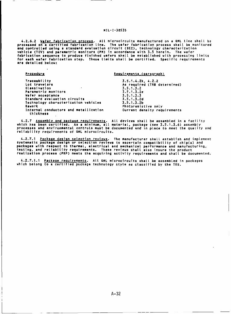
NIL-I-38535
4.2.6.2 wafer fabrication process. ALL microcircuits manufactured on a QML Line shall baprocessed on a certified fabrication Line. The wafer fabrication process shalL be monitoredand controlled using a standard evaluation circuit (SEC), technology characterizationvehicte (TCV) and parametric monitors (PM) in accordance with 3.5 herein. The waferfabrication sequence to produce finished wafers shalt be established with processing limitsfor each wafer fabrication step. These limits shall be certified. Specific requirementsare detailed below:
Procedure Roeauirments (oar graph)
Traceability 3.5.1.4.2k, 4.2.2Lot travelers As required (TRB determined)GLassivationt 3.5.1.3.2Parametric monitors 3.5.1.3.2eWafer acceptance 3.5.1.3.3Standard evaluation circuits 3.5.1.3.2dTechnology characterization vehicles 3.5.1.3.2bRework Photoresistive onlyInternlt conductors and metallization Current density requirementsthickness
4.2.7 Assembly and Package requirements. All devices shall be assembled in a facilitywhich has been certified. As a minimum, all material, package (see 3.5.1.3.6) assemblyprocesses and environmental controls must be documented and in pLace to meet the quality andreliability requirements of OML microcircuits.
4.2.7.1 Package design selection reviews. The manufacturer shatl establish and implementsystematic package design or selection reviews to ascertain compatibility of chip(s) andpackages with respect to thermal, electrical and mechanical performance and manufacturing,testing, and reliability requirements. These reviews shall also insure the productrealization process (PRP) meets the acquiring activity requirements and shall be documented.
4.2.7.1.1 Package requirements. All QML microcircuits shall be assembled in packageswhich belong to a certified package technology style as classified by the TRB.
A-32

NIL-i-38535
4.2.7.2 Assembly process procedures. The following assembly process procedures, shall be
used, as applicable, to assemble OHL microcircuits. The manufacturer shall control allphases of the assembly Line to ensure that contamination from any source or equipmentoperation and human intervention does not degrade the reliability of the assembly process orOL microcircuit. Specific requirements are shown below:
Assembly and package procedure Requirements
Incoming inspection 3.5.1.3.5aEutectic die attach Test method 2010, 3.5.1.3.5aNon-eutectic die attach Test method 2010, 3.5.1.3.5a,
Test method 5011 (as applicable)Internal visual Test method 2010, 3.5.1.3.5aHermeticity Test method 1014, test method 1018Handling 3.5.1.3.5aHuman contamination 3.5.1.3.5aRework 3.5.1.3.5a, 4.2.7.3Internal water vapor content Test method 1018, 3.5.1.3.5c
4.2.7.3 Assembly rework requirements. ALl OHL microcircuits rework procedures shall becertified. Only rebonding of wires bonded with manual wire bonding equipment is permittedon microcircuit assemblies prior to lid seal. No delidding or package opening for reworkshall be permitted for OL microcircuits. Allowable rework of sealed packages includesrecleaning of any microcircuit or portion thereof, any remarking to correct defectivemarking and lead straightening.
4.2.8 Electrical test. ALL OHL microcircuits shall be electrically tested over thespecified temperature range in accordance with the device procurement specification in acertified test facility before delivery of the product.
4.3 Screeninq. All OL integrated circuits shalt be subjected to and pass the screensspecified in table IX, herein. The procedures and accept and/or reject criteria for thetable IX screens shall have been certified by the qualifying activity. The manufacturer,through its TRB, may elect to eliminate or modify a screen based on empirical reliabilitydata which indicates that for the OHL technology, the change is justified. If such a changeis implemented, the manufacturer is still responsible for providing product which meets allof the performance, quality, and reliability requirements herein. Notification of suchchanges, deviations or eliminations must be made to the qualifying activity in accordancewith 3.4.3.2 requirements.
4.3.1 Screen testing failures. Devices which fail any screen test shall be removed atthe time of observation or immediately at the conclusion of the test in which the failurewas observed. Once rejected and verified as a device failure, no retesting is allowed. Useof electrical rejects for nonelectrical tests must meet the certified procedures and shallbe :he exception. Catastrophic failures (i.e., shorts or opens measurable or detectable at251C) subsequent to burn-in shall be analyzed. Analysis of catastrophic failures may belimited to a quantity and degree sufficient to establish failure mode and cause and theresults shall be documented and made available to the qualifying activity. A summary of theresults shall be included in the status report.
4.3.2 Screening resubmission criteria. When it has been established that a failuresduring screening tests is due to operator error or equipment failure and it has beenestablished that the remaining OHL microcircuits have not been damaged or degraded, thesurviving microcircuits, as the case may be, may be resubmitted to the corrected screeningtest(s) in which the error occurred. Failures verified as having been caused by testequipment failure or operator error shall not be counted in the PDA calculation (whenapplicable). ESD failures shall be counted as rejects and shall not be attributed toequipment failure or operator error.
-33

MIL-1-38535
4.3.3 Electrostatic discharge sensitivity. Electrostatic discharge sensitivity testingshalt be done in accordance with test method 3015 of MIL-STD-83, and the devicespecification, and marked in accordance with the marking provisions in 3.7 herein. Unlessotherwise specified, tests shalt be performed for initial qualification and product redesignas a minimum. Devices shalt be handled in accordance with MIL-HDBK-263 and MIL-STD-1686 tosafeguard against discharge damage (see 3.5.1.3.4).
4.3.4 Internal visual inspection. Internal visual inspection shalt be performed to therequirements of test method 2010, condition B of NIL-STD-883. Hicrocircu~ts awaitingpreseal Inspection, or other accepted, unsealed microcircuits awaiting further processingshall be stored in a dry, inert, controlled environment until sealed. The alternateprocedure of test method 5004 of MIL-STD-883 shalt be used when any of the followingcriteria are met:
a. Minimum horizontal geometry is Less than three microns.
b. Metallization consists of two or more levels.
c. Opaque materials mask design features.
4.3.5 Constant acceleration. All microcircuits shalt be subjected to constantacceleration, in the Y1 axis only, in accordance with test method 2001, condition E(minimum) of MIL-STD-883. Microcircuits which are contained in packages which have an innerseat or cavity perimeter of two inches or more in total length or have a package mass offive grams or more may be tested by replacing condition E with condition D in method 2001.
4.3.6 Burn-in. Burn-in shalt be performed on all QML microcircuits at their maximumrated operatins temperature. For microcircuits whose maximum operating temperature isstated in terms of ambient temperature, TA, table I of test method 1015 of MIL-STD-883applies. For microcircuits whose maximum operating temperature is stated in terms of casetemperature, T , and where the ambient temperature would cause Tj to exceed +175"C, theambient operat9ng temperature may be reduced during burn-in from 125'C to a value that willdemonstrate a T between +1751C and +200"C and T equal to or greater than 125"Cwithout changini the test duration. Data supporiing this reduction shalt be available tothe acquiring and qualifying activities upon request.
4.3.7 Final electrical measurements. Final electrical testing of microcircuits shaltassure that the microcircuits tested meet the electrical requirements of the deviceprocurement specification and shall include, as a minimum, the tests of Group A, subgroups1, 2, 3, 4 or 7,, 5 and 6 or 8, and 9, 10 and 11.
4.3.8 Seat (fine and gross leak) testing. Fine and gross teak seat tests shalt beperformed between temperature cycling and final electrical testing after ail shearing andforming operations on the terminals in accordance with MIL-STD-883 method 1014.
4.3.9 Pattern failures. Pattern failure criteria may be used as an option for any screen
provided that:
a. Inspection tot size is less than 500 microcircuits.
b. Preburn-in testing is done.
A maximum number of pattern failures (failures of the same part type when the failures arecaused by the same basic failure mechanism) shalt apply as specified in the acquisitiondocument. If not otherwise specified, the maximum allowable pattern failures shalt befive. Accountability shalt include burn-in through final electrical test.
A-34
MIL-1-38535
4.3.9.1 Pattern failure rejects. When the number of pattern failuresexceeds the specified limits, the burn-in Lot shalt be rejected. At themanufacturer'l TRB option, the rejected tot may be resubmitted to burn-in onetime provided:
a. The cause of the failure has been determined and evaluated.
b. Appropriate and effective corrective action has been completed toreject all microcircuits affected by the fa".ure cause.
c. Appropriate preventive action has been initiated.
4.4 Technology conformance inspection (TCI). TCI testing shall beaccomplished by the manufacturer on a periodic basis to assure that themanufacturer's quality, reliability, and performance capabilities meet therequirements of the QM plan. The manufacturer of QNL microcircuits shall becertified by the qualifying activity to use one or both of the technologyconformance inspection (TCI) procedures described below. The two TCIprocedures are end-of-Line OC (option 1) and in-line control (option 2).
4.4.1 General. Any QML or SEC integrated circuit used for either TCI option(see 4.4.2 or 4.4.3) must be screened in accordance with 4.3 requirements.
4.4.1.1 TCI reportinq. Summary of TCI tests analysis shalt be submitted tothe qualifying activity in accordance with 3.4.5 requirements. If TCIrequirements are not met, the technology review board shall notify thequalifying activity immediately and all products manufactured and deliveredbetween the last TCI and the failed TCI shall be placed in suspect status. Themanufacturer shall analyze the failure, determine the reason for failure andsubmit a corrective action plan. An assessment of whether to recall allsuspect products shall be made by the TRB and the qualifying activity shall benotified of the decision. Recertification and requalification of the QML Linemay be required based on the nature of the problem and action taken by themanufacturer. Procedures for standard OCI and in-line control for a QHL Lineare described in the following paragraphs.
4.4.2 Standard quality conformance inspection testing (option 1).End-of-Line OCI testing shall be performed every OCI interval, as recommendedin table VIII herein. Each end-of-line QCI vehicle shall pass the end-of-Linequality conformance. ALL group A, 9 and E testing shall be performed onmicrocircuits to be delivered as QML microcircuits. Group C and D testingshalt be done on either the SEC or QML microcircuits. Groups A,B,C,D, and Erequirements are found in tables III thru VII, herein.
NOTE: If a manufacturer elects to eliminate a quality conformance inspectionstep by substituting an in-process control or statistical process controlprocedure, the manufacturer is only relieved of the responsibility ofperforming the OCI operation associated with that step. The manufacturer isstill responsible for providing a product which meets all of the performance,quality, and reliability requirements herein and in the device procurementspecification. Documentation supporting substitution for OCI shalt be ietainedby the manufacturer and avail3bte to the qualifying activity upon request.
Each group may contain individual subgroups for the purposes of identifyingindividual tests or groups of tests. Subgroups within a group of tests may beperformed in any sequence but individual tests within a subgroup (except group8, subgroup 2) shalt be performed in the sequence indicated for groups 5, C, D,and E tests herein. Electrical reject devices from the same inspection tot maybe used for all subgroups when electrical end-point measurements are notrequired.
A-35

NIL-I-38535
4.4.2.1 Group A inspection. Group A inspection shaLt be performed on each inspectiontot and shaLt consist of eLectricaL parameter tests specified for the specified device.Group A inspection may be performed in any order.
4.4.2.2 GrOuD 8 Inspection. Group 3 inspection shaLt be performed on each inspectiontot, for each qualified package type and Lead finish. Group B shaLt consist of mechanicaland environmental tests for the specified device class. Resubmission procedures shalt bedocumented In the ON plan. For solderability, a statistical sound sample size consistingof Leads from several packages shall be tested with zero (0) failures. The actual numbershalt be determined by the TRI and detailed in the TCI procedures in the ON plan.
4.4.2.3 group C inspection. Group C inspection shaLL IncLude die-related testsspecified which are performed periodically. Resubmission procedures shalt be documented inthe ON plan. Where group C endpoints are done on actual devices, group C endpoints shaltbe specified in the device procurement specification.
4.4.2.4 Group D inspection. Group D inspection shall include package related testswhich are performed periodicaLly, Resubmission procedures shall be documented in the OMplan. Where group D endpoints are done on actual devices, group D endpoints shalt bespecified in the device procurement specification.
4.4.2.5 End-point tests for groups 6 .C. D. (E if applicable). End-point measurementsand other specified post-teat measurements shalL be made for each sample after completionof lt other specified tests in the subgroup. The test Limits for the end-pointmeasurements shall be the same as the test Limits for the respect.ive group A subgroupinspections. Different end-points may be specified for group E tests in the detailspecifications. Any additional end-point electrical measurements may be performed at thediscretion of the manufacturer.
4.4.2.6 End-of-line OCT testing. ALl microcircuits used In end-of-line OCI testing thatmeet the requirements of this document and the device procurement specification shaLl beidentified and delivered to the acquiring activity as ONL microcircuits upon approval ofthe manufacturer's TRB.
4.4.3 in-line control testing (option 2). In-line control testing shalt be performedthrough the use of the approved SEC or OML microcircuit. The in-line control test planshalt show how aLl the group A, B, C and 0, test conditions are incorporated under SPC orprocess control to stto: in-Line control monitoring. Group E tests shaLl be done on eachOHL microcircuits as applicable. The following shall also apply.
4.4.3.1 Group A electrical testing. Group A electrical testing shall be satisfied byin-line inspections performed in accordance with the applicable procedure of MIL-STD-883 onactual devices.
4.4.3.2 Group C life tests. Life tests shall be performed on the SEC at intervals setby the TRB in the quality management plan.
A-36

MIL-1-38535
TABLE III. Group A electrical tests. 1/
Subgroup Parameters Quantity (accept no.)
1 Static test at +25-C 116(0)2 Static tests at maximun 116(0)
rated operating temperature3 Static tests at minimum 116(0)
rated operating temperature
4 Dynamic test at +25"C 116(0)5 Dynamic tests at maximum 116(0)
rated operating temperature6 Dynamic tests at minimum 116(0)
rated operating temperature
7 Functional test at +25*C 116(0)8 Functional tests at maximum 116(0)
and minimum rated operatingtemperatures
9 Switching tests at +25"C 116(0)10 Switching tests at maximum 116(0)
rated operating temperature11 Switching tests at minimum 116(0)
rated operating temperature
1/ The specific parameters to be included for tests in each subgroup shall beas specified in the device procurement specification. Where no parametershave been identified in a particular subgroup or test within a subgroup, nogroup A testing is required for that subgroup or test to satisfy group Arequirements.
TABLE IV. Group B tests.
MIL-STD-883Minimum sample size
Subgroup Test Method Condition Quantity (accept no.)
1 Resistance to 2015 A or B 4(0)solvents
2 Bond strength 2011 22(0)(1) Thermo compression (1) C or D(2) ULtrasonic (2) C or D(3) FLip-chip (3) F(4) Beam Lead (4) H
Die shear test 2019 die size
3 Solderability 2003 or solder See 4.4.2.22022 temperature
2451C t5"C
A-37

MIL-1-38535
TABLE V. Group C tests.
M MIL-STD-883 QuantityTest Method Condition (accept no.)
Subgroup 1 1005 Test condition 45(0)a. Steady state to be specified
Life test (1,000 hrs at 125"C)
b. End-point As specified in theelectrical applicable deviceparameters procurement
specification
TABLE VI. Group D tests.
MIL-STD-883 QuantitySubgroup Test Method Condition (accept no.)
I a. Physical dimensions 2016 15(0)
2 a. Lead integrity 2004 82 Fatigue 15(0)b. Seal
(1) Fine 1014 As appLicabLe(2) Gross 1014 As applicable
3 a. Thermal shock 1011 B, 15 cycles 15(0)b. Temperature cycling 1010 C, 100 cyclesc. Moisture resistance 1004d. Seat 1014 As applicable
(1)Fine(2)Gross
e. Visual 1004, 1010f. End-point As specified
electricals in the applicabledevice procurementspecification
4 a. Shock 2002 S 15(0)b. Vibration, variable 2007 A
frequency*c. Acceleration 2001 E, Y1 orientationd. Seat 1014 As applicable
(1) Fine(2) Gross
e. Visual examinationf. End-point electricals As specified
in the applicabledevice procurementspecification
5 a. Salt atmosphere 1009 A 15(0)b. Seat 1014 As applicable
(1)Fine(2)Gross
6 a. Internal water vapor 1018 5000 ppm 100"C 3(0) or 5(0)
,7 a. Adhesion of Lead finish 2025 15(02
8 a. Lid torque 2024 glass frit seal only 5(0)
A-38

MIL-1-38535
TABLE VII. Center group E (RHA testing)(radiation hardness assurance tests) j/
_ _ _ MIL-STD-883Quantity I/
Test Method Condition RHACL/SPEC j/ (accept no.)
Subgroup 1Neutron 2/ 1017 +25"C >10 0(0)
irradiation >2 s10 5(0)
Endpoint As specified in theelectrical applicable deviceparameters procurement
specification
Subgroup 2Total ionizing 1019 +25°C >10 0(0)
radiation dcse >2 10 5(0)
Endpoint As specified in theelectricaL applicable deviceparameters procurement
specification
1_/ Parts used for one subgroup test may not be used for other subgroups but may be usedfor higher Levels in the same subgroup. Total dose exposure shall not be consideredcumulative unless testing is performed within the time limits of the test method.
2/ Not required for MOS devices unless bipolar elements are included by design.
3/ Per wafer lot. Alternatively, each wafer may be accepted on a 2(0) quantity (accept)number. If the alternate is chosen, a PDA of 10% or equivalent shall apply to the lot.
j/ The RHACL/SPEC is the ratio of the capability level to the specification level offluence.
TABLE Vill. Standard OCT testing procedure. 1/
Table OCI requirements OCI vehicle Interval
Table III Group A electrical Actual device Each inspection lottesting
Table IV Group B testing Actual device Each inspection totTable V Group C testing SEC or actual device Every 3 monthsTable VI Group D testing SEC or actual device Every 6 monthsTable VII Group E testing Actual device Each wafer lot
I/ Each group may contain individual subgroups for the purposes of identifyingindividual tests or groups of tests.
A-39

MIL-1-38535
TABLE IX. Microcircuit screening procedure for QML microcircuits.
Screen MIL-STD-883 test method and condition
Electrostatic discharge sensitivity 3015 (see 4.3.3, Initial qualificationonly)
Wafer acceptance TRB plan isee 3.5.1.3.3)
Internal visual 2010, test condition a (see 4.3.4)
Temperature cycling 1010, test condition C, 50 cycles minimum
Constant acceleration 2001, test condition E (minimum)Y1 orientation only (see 4.3.5)
Serialization In accordance with device procurementspecification
Burn-in test 1015, 160 hrs at +1251C minimum(see 4.3.6)
Interim (pre-burn-in) In accordance with device procurementelectrical parameters specification
Interim (post-burn-in) In accordance with device procurementelectrical parameters specification
Percent defective 5% or TRB determined, all lotsallowable (PDA) calculation (subgroup 1 table 1i)
Final electrical test In accordance with device procurementa. Static tests (table III) specification
1. +256C2. Maximum and minimum
rated operating temperatureb. Dynamic or functional
tests (table I1)1. +250C2. Maximum and minimum
rated operating temperaturec. Switching tests (table III)
1. +25"C2. Maximum and minimum
rated operating temperature
Seal 1014a. Fineb. Gross
External visual 2009
5. PACKAGING.
5.1 Packaging requirements. The requirements for packaging shal be in accordance withMIL-M-55565.
A-40

MIL-1-38535
6. NOTES
6.1 Intended use. This specification is intended to support governmentMicrocircuit application and logistic programs. Detailed characteristics ofmicrocircuits needed for a program are to be defined by the device procurementspecification.
6.2 Terms and definitions. For the purpose of this specification, the terms, anddefinitions of MIL-STD-883 and MIL-STO-1331, and those contained herein shall applyand shat be used in the applicable device procurement specifications wherever theyare pertinent.
6.2.1 Microelectronics, That area of electronic technology associated with orapplied to the realization of electronic systems from extremely small electronic partsor elements.
6.2.2 Element (of a microcircuit or integrated circuit). A constituent of themicrocircuit or integrated circuit that contributes directly to its operation.
6.2.3 Substrate (of a microcircuit or integrated circuit). The supporting materialupon or within which the elements of a microcircuit or integrated circuit arefabricated or attached.
6.2.4 Integrated circuit (microcircuit). A small circuit having a high equivalentcircuit element density, which is considered as a single part composed ofinterconnected elements on or within a single substrate to perform an electroniccircuit function.
6.2.4.1 Nultichip microcircuit. An integrated circuit or microcircuit consistingof elements formed on or within two or more semiconductor chips which are separatelyattached to a substrate or package.
6.2.4.2 Monolithic microcircuit. An integrated circuit or microcircuit consistingexclusively of elements formed in situ on or within a single semiconductor substratewith at least one of the elements formed within the substrate.
6.2.5 Microcircuit module. An assembly of integrated circuits or an assembly ofintegrated circuits and discrete parts, designed to perform one or more electroniccircuit functions, and constructed such that for the purposes of specificationtesting, commerce, and maintenance, it is considered indivisible.
6.2.6 Production lot. A production tot shall consist of devices manufactured onthe same production line(s) (QM technology flow) by means of the same productiontechnique, materials, controls, and design.
6.2.7 Inspection tot. A quantity of integrated circuits submitted at one time forinspection to determine compliance with the requirements and acceptance criteria ofthe applicable device procurement specification. Each inspection tot shall bemanufactured on the same production tine through final seat by the same productiontechniques.
6.2.8 Wafer tot. A wafer tot consists of integrated circuit wafers formed into alot at the start of wafer fabrication for homogeneous processing as a group, andassigned a unique identifier or code to provide traceability.
6.2.9 Percent defective allowable (PDA). Percent defective allowable is themaximum observed percent defective which will permit the Lot to be accepted after thespecified 100 percent test.
6.2.10 Delta Limit. The maximum change in a specified parameter reading which willpermit a device to be accepted on the specified test, based on a comparison of thepresent measurement with a specified previous measurement. Note: When expressed as apercentage value, it shalt be calculated as a proportion of the previous measuredvalue.
A-41

MIL-1-38535
6.2.11 Rework. Any processing or reprocessing operation documented in accordancewith the manufacturer's ON plan, other than testing, applied to an individual device,or part thereof, and performed subsequent to the prescribed nonrepairing manufacturingoperations which are applicable to all devices of that type at that stage.
6.2.12 Final seat. That manufacturing operation which completes the enclosure of adevice so that further internal processing cannot be performed without disassemblingthe device.
6.2.13 Acquiring activity. The organizational element which contracts forarticles, supplies, or services; or it may be a contractor or sub-contractor when theorganizational element has given specific written authorization to such contractor orsubcontractor to serve as agent of the acquiring activity. A contractor orsubcontractor serving as agent of the acquiring activity shall not have the authorityto grant waivers, deviations, or exceptions to this specification unless specificwritten authorization to do so has been given by the organization (i.e., preparingactivity, qualifying activity).
6.2.14 Ouatifying activity. The organizational element of the Government thatgrants certification, and qualification for the specific technology flow in accordancewith this specification.
6.2.15 Parts per million (PPM). Parts per million shall be as defined in JEDECPublication 16.
6.2.16 Device type. The term device type refers to a single specific microcircuitconfiguration.
6.2.17 Die type. A microcircuit manufactured using the same physical size,materials, topology, mask set, process flow, on a single fabrication Line.
6.2.18 Radiation hardness assurance (RHA). The portion of product assurance whichinsures that parts continue to perform as specified or degrade in a specified mannerwhen subjected to the specified radiation environmental stress.
6.2.19 Etectrostatic discharge sensitivity (ESD). Electrostatic dischargesensitivity is defined as the level of susceptibility of a device to damage by staticelectricity. The level of susceptibility of a device is found by CSDS classificationtesting and is used as the basis for assigning on ESDS class.
6.2.20 Package family. A group of package types with identical configuration andprocess techniques (e.g. cerdip, side braze, cerpack).
6.2.21 Technotooy flow. A technology flow is that specific manufacturing line fromdesign, fabrication, assembly, packaging, and test in a given technology from which amanufacturer designs, builds, and tests integrated circuits. Once a manufacturer'stechnology flow has been certified and qualified by the qualifying activity, it islisted on the Qualified Manfuacturer's Listing (OML).
6.2.22 Qualified manufacturer's tisting (.O.M. The qualified manufacturer'slisting is that Listing which defines and specifies the certified and qualifiedtechnology flow of a manufacturer from which OML integrated circuits may be purchased.
6.3 Discussion. The foundation of generic qualification is the instillment ofquality management (QN) within the manufacturing environment. Quality management (OM)requires that all Levet3 of management and nonmanagement be actively involved in thecommitment to quality. Also, a technology review board (TRB) must be established tocontrol, stabilize, monitor and improve the qualified technology. The TRB shaltdevelop a quality management plan that outlines how the manufacturing operation for agvan technology is controlled, monitored and improved throughout its entire "Lifecycle". Key aspects of this plan are the establishment of statistical processcontrol, field failure return programs, corrective action procedures, qualityimprovement and any other approaches required to control and improve product qualityand reliability. These requirements are detailed in this document.
A-42

MIL-I-38535
Further, this document describes procedures and requirements for manufacturer's listingon the Qualified Manufacturer List (QML) for integrated circuits. Manufacturers listedon the QML wilt be able to produce microcircuits without the need for extensiveend-of-manufacturing qualification testing and quality conformance inspections on eachdevice design. The reduction of the end-of-manufacturing testing will be replaced within-line monitoring and testing and statistical process controls (SPC). Also, surrogatedevices, such as the standard evaluation circuit (SEC) wilt be used to assess thetechnology's reliability. Introduction of this methodology shifts the emphasis fromthe need of individual microcircuit qualification to process (technology) certificationand qualification. This wilt accelerate the microcircuit insertion cycle of highquality and reliable microcircuits.
The generic qualification philosophy, leading to QML, is a process by which amanufacturer acquires a manufacturing line or technology flow certification andqualification. ongoing monitoring techniques wilt be used to maintain QML status. Themanufacturing line consists of facilities and procedures appropriate to accomplish thedesign, mask making, wafer fabrication, assembly, package and testing of microcircuits(see figure 2). Figure 3 illustrates six possible combinations of a manufacturing lineutilizing three design centers, two mask fabrication facilities, three waferfabrication facilities, two package and assembly sites and two test facilities. Theprocedure of generic qualification is accomplished in two stages; certification andqualification. The process of certification is the recognition of evidence by thequalifying activity that the manufacturing line is capable of producing microcircuitsof high quality and compliant with the requirements of this document. Qualification isthe actual demonstration of the certified manufacturing line capabilities by producing"first pass" microcircuits compliant with the requirements of this document and thedevice specification. In figure 3, each block can be individually reviewed, but must becertified as a flow. The only process flow which would be qualified (OML Listed) wouldbe the group of blocks which are linked together and tested during qualification. Theletters "A" and "5" indicate a QML flow where qualification testing has qualified a
complete path. The other paths are not QML until certification and qualificationtesting of the processes is done.
OM does not stop with a manufacturer listed on the CML. This specification identifiesthe necessary screens which still must be done on each device built. These screens canbe reduced or changed by the manufacturers' TRB when gathered reliability data on thetechnology indicates that such changes are substantiated. The philosophy of genericqualification incorporates the idea that high quality and reliable microcircuits can beobtained without excessive testing if the processes are properly monitored andcontrolled at each step of the manufacturing line. The following describes themonitors and controls which may be used.
a. The design procedure and tools are controlled in such a manner that theensuing microcircuit design performs only with limits that have been shown tobe reliable for the technology being used, within the constraints ofestablished design rules (electrical, geometric and reliability).
b. The mask fabrication facility is controlled such that an error free mask isproduced from the microcircuit design database. Monitoring, controlling andreducing defect density is helpful in obtaining error free masks.
c. The wafer fabrication process is controlled with the following: use of in-linestatistical control; a parametric monitor (PM) structure for measuringelectrical parameters; a technology characterization vehicle (TCV) structureto study intrinsic reliability mechanisms; and a standard evaluation circuit(SEC) to monitor the fabrication process and to serve as a surrogatemicrocircuit for reliability testing.
d. The package and assembly facility is controlled with emphasis on in-linestatistical process control of all assembly steps.
e. The test area controls consist of test equipment accuracy and calibration aswell as a controlled interface to the microcircuit design center.
A-43

MIL-I-38535
f. The overall control of the processes are under the auspices of a technologyreview board (TRB) which is established by the manufacturer. The TRB issolely responsible for the QML flow that hos been certified and qualified.
g. For radiation hardness assurance (RHA) devices, procedures and requirementsare integrated into this document for establishing and demonstrating aradiation hardness assurance capability level (RHACL) for the technology.Many device oriented tests can be reduced or eliminated when correlation datafor models and test structures have been established by the TRB. The mainconcern in the RHA community is whether the device specification accuratelydescribes the device performance in the radiation environment specified.Until such models and test structures are developed, some actual deviceradiation testing will be required.
h. Appendix B to this specification defines an implementation transistionapproach which may be used for space or other critical environmentapplications.
6.4 Additional reference documents. The following documents are not directlyreferenced herein but should be used as guidelines.
DHA-TR-36-38 Hardness Assurance Guidelines for MIL-HDBK-339 (USAF).
FED-STD-209 - Clean Room and Work Station Requirements, ControlledEnvironments.
MIL-HDBK-279 - Total Dose Hardness Assurance Guidelines for Semiconductors andMicrocircuits.
MIL-HDBK-280 - Neutron Hardness Assurance Guidelines for Semiconductors andMicrocircuits.
MIL-HDBK-339 Custon Large Scale Integrated Circuit for Space Applications.
MIL-STD-45662 - Calibration S ,tems Requirements.
AMERICAN SOCIETY FOR TESTING AND MATERIALS (ASTM)
ASTM 8487-79 - Measurement of Metal and Oxide Coating Thicknesses byMicroscopical Examination of a Cross Section.
ASTM B567-79A - Measurement of Coating Thickness by the Beta Backscatter Method.
(Application for copies should be addressed to the American Society for Testingand Materials, 1916 Race Street, Philadelphia, PA 19103.)
ELECTRONIC INDUSTRIES ASSOCIATION (EIA)
EIA-STD-5 Packaging Materials Standard for Prorection of ElectrostaticDischarge Sensitive Devices.
JEDEC Publication
95 JEDEC Registered and Standard Outlines for SemiconductorDevices.
16 Assessment of Microcircuit Outgoing Quality Levels in Parts PerMillion (PPM).
(Appiication for copies should be addressed to the Electronic Industriesassociation, 2001 Eye Street, N.W., Washington, DC 20006.)
A-44

MIL-1!38535
FIGURE 2. The OML rmrfacturing tine.
AA IFAB I A
FDESIGN
FIGURE 3. Cominations of a manufacturing tine
A-45

NIL-1-38535
6.5 Subiect term (key word) listings:
AppLication specific integrated circuit (ASIC)Computer automated design (CAD)Design-for-test (DFT)Design rule ch.eck (DRC)ElectricaL rule check (ERC)ELectrostatic discharge sensitivity (ESD)FaiLure analysis (FA)Joint test action group (JTAG)Linear energy threshold (LET)Mean-time-to-faiture (MTF)Original equipment manufacturer (OEM)Parametric monitor (PM)Post irradiated endpoint parameter Limits (PIPL)Qualified manufacturer Listing (QML)Quality assurance (QA)Quality management (QM)Radiation hardness assurance (RHA)Radiation hardness assurance capability Level (RHACL)Single event phenomena (SEP)Single event upset (SEU)Standard evaluation circuit (SEC)Statistical process control (SPC)Technolagy characterization vehicle (TCV)Technology conformance inspection (TCI)Technology review board (TRB)Tester independent support software system (TISSS)Time dependent dielectric breakdown (TDDS)Very high speed integrated circuit (VHSIC)VHSIC hardware description Language (VHDL)
A-46
MIL-1-38535
APPENDIX A
DEVICE PROCUREMENT SPECIFICATION
10. SCOPE
10.1 Scope. This appendix contains the details of the device procurementspecification requirements needed to define individual microcircuit types forprocurement. This appendix is a mandatory part of the specification.
20. APPLICABLE DOCUMENTS. This section is not applicable to this appendix.
30. DEVICE PROCUREMENT SPECIFICATION
30.1 Scope. This drawing describes device requirements in accordance withMIL-I-38535 QML devices.
30.2 PIN. The complete part or identifying number (PIN) shalt be in acct. ncewith MIL-I-38535 (see 3.7.2.).
30.2.1 Device types. The device types shalt identify the circuit function asfo11ows:
Device type Generic number Circuit function
30.2.2 Case outlines. The case outlines shalt be designated as appropriate to therequirements of MIL-I-38535 and as follows:
Outline letter Case outline
30.2.3 Lead finish. The Lead finish shalt be as specified in MIL-I-38535.
30.3 Absotute maximum ratings for usage. 1/
Operating temperature rangePositive supply voltageNegative supply voltageInput voltagePower dissipation (P )Storage temperature angeLead temperature (soldering, 10 seconds)Thermal resistance, junction-to-case (9Electrostatic discharge sensitivity (ESdg)G-ForceOther parameters (device specific)
30.4 Recommended operating conditions.
Operating temperature range (case (Tc) or ambient (TA) as appropriate fortechnology)
Supply voltagesOther parameters (device specific)
1/ Stresses above the absolute maximum ratings may cause permanent damage to thedevice. Extended operation at the maximum revels may degrade performance and affectreliability.
A-47

MIL-1-38535
APPENDIX A
30.5 LoJcia tsting.Fault coverage measurement of manufacturing Logic tests, test method 5012 of
NIL-STD-883.
40. APPLICABLE DOCUMENTS
40.1 Government specification and standard. UnLess otherwise specified, the followingspecification, and standard of the issue Listed ir chat iisue of the Department ofDefense Index of Specifications and Standards specified in the solicitation, form a partof this drawing to the extent specified herein.
SPECIFICATION
MILITARY
MIL-I-38535 - Integrated Circuits (Microcircuits) Manufacturing, GeneralSpecification for.
STANDARD
MIL-STD-883 - Test Methods and Procedures for Microelectronics.
40.2 Order of precedence. In the event of a conflict between the text of this drawingand the references cited herein, the text of this drawing takes precedence.
50. REQUIREMENTS
50.1 Item requirements. The individual item requirements shalt be in accordance withMIL-I-38535 and as specified herein.
50.2 Etectrical test requirements. The electricat test requirements shalt be inaccordance with table II herein. The electrical tests for each subgroup are defined intable I herein.
50.3 Design. construction, and physical dimensions. The design, construction, andphysical dimensions shalt be in accordance with MIL-1-38535 and described herein.
50.3.1 Terminal connections. The terminal connections shalt be as specified on figure1 herein.
50.3.2 Truth table. The truth table (if applicable) shalt be as specified onfigure 2 herein.
50.3.3 Functional description. Figure 3 shalt provide a brief description of thedevice function (block diagrams are recommended).
50.3.4 Case outline. The case outtine shalt be in accordance with 30.2.2 herein andas specified on figure 4.
50.3.5 Burn-in circuit. The device burn-in circuit shalt be as specified onfigure 5.
50.3.6 Radiation exposure circuit (when applicable). The radiation exposure circuitshalt be as specified on figure 6.
50.4 Electrical performance characteristics. Unless otherwise specified, theelectrical performance characteristics are as specified in tab(e I end apply over thefutl operatfna tempereturP rtne=.
A-48

MIL-1-38535
APPENDIX A
50.4.1 RNA environments (when eotigabte). PIPL and delta limits (when applicable)
shaLl be specified in table I for the specified RHA environments.
50.5 Marking. Marking shaLL be in accordance with NIL-i-38535.
60. QUALITY ASSURANCE PROVISIONS
60.1 SamtLing and inspection. SampLing and Inspection-procedures shaLl be inaccordance with NIL-1-38535.
60.2 Screening. Screening shaLl be in accordance with MIL-1-38535 and shall beconducted on aLl devices.
60.2.1 Value added screens. Any value added screen beyond the requirements ofMIL-1-38535 shall be detailed in table I1.
60.3 Technology conformance inspections. Technology conformance inspections shaLL
be in accordance with NIL-1-38535.
70. PACKAGING
70.1 Packaging requirements. The requirement for packaging shall be in accordancewith iL-1-38535.
80. NOTES
TABLE I. Electrical performance characteristics.
Test Symbol Conditions Group A Limits UnitTemperature Subgroups Min MaxRange, RHAEnvironment
List specific tests with parameters.
TABLE Ii. Electrical test requirements.
Test requirements Subgroups
Interim electrical parameters In accordance with MIL-1-38535Final electrical test parameters and the device procurementGroup A test requirements specificationGroup C and D end-point electricals
A-49
NIL-1-38535
APPENDIX A
TABLE 111. Vatue added screens.
Test Requirements
List tests As appropriate in accordance with Appendix Bof NIL-I-38535
Figure 1. Terminal connectionsFigure 2. Truth tabteFigure 3. Functional descriptionFigure 4. Package outtineFigure 5. Burn-in circuitFigure 6. Radiation exposure circuit
A-50
MIL-1-38535
APPENDIX B
SPACE APPLICATION
10. SCOPE
10.1 Scope. This appendix presents the requirements which shalt be used tosupplement MIL-1-38535 for space system microcircuits. This appendix is intended to bea transitional document.
10.2 Application. When specified by the procurement document (i.e., purchaseorder), the requirements of this appendix shalt become a part of HIL-1-38535 and beimplemented as specified herein.
20. APPLICABLE DOCUMENTS
20.1 Government documents.
20.1.1 Specifications and standards. The following specifications and standardsform a part of this specification to the extent specified herein. Unless otherwisespecified, the issues of these documents shalt be those Listed in the issue of theDepartment of Defense Index of Specifications and Standards (DODISS) and supplementthereto, cited in the solicitation.
STANDARD
MILITARY
MIL-STD-454 Standard General Requirements for Electronic Equipment.
30. REOUIREMENTS
30.1 General. Microcircuits supplied to this document shalt be manufactured andtested in accordance with approved basetines and the requirements herein. The TRBshalt not make major changes to the baseLined processes, procedures, or testing withoutnotifying the qualifying activity prior to implementation of the change for the deviceprocurement specification in question.
30.1.1 Acquiring activity. When specified by the procurement document, theacquiring activity may:
a. Require prior notification of major changes to the baseLined processes,procedures, or testing.
b. Require independent verification of wafers (unprobed) or packaged devices(TCV, SEC, or actual devices) by OEMs or Government agencies.
c. Request screening and TCI summary data be delivered with the devices.
30.2 Confticting requirements. In the event of conflict betweeen the requirementsof this appendix and other referenced documents, the order of precedence shalt be asfoI lows:
a. The acquisition document (purchase order).
b. Applicable device procurement specification.
c. This appendix.
d. MIL-1-38535.
e. Specifications, standards, and other documents referenced in 2.1 ofMIL-1-38535.
A-51

NIL-1-38535
APPENDIX B
NOTE: The acquisition document may specify additional requirements, but shall not
reduce or waive any requirements.
30.3 Validation (certification). Validation of a manufacturing Line for productionof integrated circuits for use in space systems shall be accomplished by a team whichincludes representatives for NASA and the Air Force Space Systems Division, in additionto the normal participation by DESC and RADC.
30.4 Manufacturing verification. When specified, the manufacturing verificationprocedure for new microcircuits shat include characterization of actual devices inincrements of ambient or case temperature, supply voltage and input voltage Levels overthe specified parameter range.
30.5 DesiOn verification. When specified, a descriptive model (i.e., VHDL), and atest vector set (i.e., tester independent support software system (TISSS) program)shaLl be avaiLable for independent verification of microcircuits in accordance withMIL-STD-454 Requirement 64.
30.6 Part number. When this appendix is imposed by contract or purchase order, a"V" mark shall be used in place of the "Q" mark in the part number format in 3.7.2.
40. QUALITY AND RELIABILITY ASSURANCE
40.1 Screening. In addition to the screening tests specified in MIL-I-38535, thevalue added screening tests specified below shatl be performed:
a. Nondestructive bond putt (.iDBP) in accordance with NIL-STD-883, test method2023, or approved alternate verified during validation, on each interconnectbond. An alternate method, if necessary, shaLl consider a 100 percent visualinspection of the elements to be bonded (i.e., bond pads and posts) prior tothe bonding operation.
b. Internal visual inspection in accordance with MIL-STD-883, test method 2010,condition A, or approved alternate verified during validation on eachmicrocircuit. An alternate method, if necessary, must address all theinspection topics of test method 2010.
c. Particle impact noise detection (PIND) in accordance with MIL-STD-583, testmethod 2020 on each device.
d. Reverse bias burn-in in accordance with MIL-STD-883, test method 1015 on eachdevice when specified in the device procurement specification.
e. Radiograph inspection in accordance with MIL-STD-883, test method 2012 on eachdevice.
f. Burn-in test in accordance with MIL-STD-883, test method 1015 on each devicefor 240 total hours at +125"C.
40.2 Technology conformance inspection (TCI). The TCI requirements listed belowapgly on each lot of deliverable devices. The group and table references correspond tothose contained in MIL-I-38535. These requirements do not replace the normal TCItesting requirements of MIL-I-38535.
a. Group A, table I1, shall be performed on actual devices. For those Lotshaving a quantity of less than 116 devices, the tests sheLl be imposed as 100percent screens and the tot accepted on zero test rejects.
A-52

IL-1-38535
APPENDIX 8
b. Group 3, table IV, shall be performed on actual devices. Dummy packages orreject devices may be used if it can be determined by the TRB that the intentof the test is not violated. The sample size of table IV is acceptableprovided the 22(0) bond strength and solderability criteria has been appliedto at Least two separate devices (i.e., 11 Leads per device), and the dieshear test is applied with a 2(0) criteria.
c. Group C, table V, shalt be performed on a quantity(accept) criteria of 22(0).For Lots greater than 200, actual devices shall be used. For Lots Less thanor equal to 200, the number of actual devices shall be the greater of 5devices or 10 percent of the lot, and the SEC shall supplement actual devicesto result in a sample'of 22.
d. Group D, table VI, shall be performed on actual devices. Subgroup tests 2a,3a, b, c, 4a, b, c, 5a, 6a, 7a, and 8a may be accomplished on dummy packagesor rejected devices if it can be determined bf the TRB that the intent of thetest is not violated. The sample size (accept criteria) for group D tot testsshall be a minimum of 2(0) except that Lead related tests shall be applied ona 22(0) basis, to at Least two separate devices (i.e., 11 Leads per device).
A-53

MIL-1-38535
CONCLUDING MATERIAL
Custodians: Preparing activity:Army - ER Air Force - 17Navy - ECAir Force - 17 Agent:NASA - NA DLA - ES
Review activities: (Project 5962-1194)Army - AR, MI, PANavy " MCAir Force - 11, 19, 85, 99DLA - ES
User activities:Army - SMNavy - AS, CG, OS, SH
Civil agency coordinating activity:DOT-FAA(RD-650)
A-54

I STANDARDIZATION DOCUMENT IMPROVEMENT PROPOSALI(See Instrucions - Revere Side)1. DOCUMENT NUMBER 2. DOCUMENT TITLE MILITARY SPECIFICATION INTEGRATED CIRCUITSMIL-I-38535 ORAN MAT TIITTS) MANIIFACTURING, GENERAL SPECIFICATION FORS 34. NAME OF SUBMITTING ORGANIZATION 4. TYPE OF ORGANIZATION (Mar'k orge)
I I -] VENDOR
b. ADDRESS (Stmet. City, Stte, ZIP Cod) MENDORER
I ! OTHER (Sp¢ecit):
5. PROBLEM AREAS
. Pacg ta0 h Number and Wordinp
Z
b. RocommenOds Wording:
f4
I [ c. Roemon/Retionalo for Recomm ndalotn:
-I
6, REMARKS
70. NAME OF SUBMITTER (Laa. Fo, MI) - Oplonol b WORK TELEPHONE NUMBER linclude Armo'.ode) - Oot'onal
C MAILING ADDRESS 'SItet. CItY. Sl te. ZIP Coder - otonal 8. oATE OF SUMISSION , YMMDD)
FDO °OR 1426 PREVIOUS EDITION IS OBSOLETE.
A-55

INSTRUCTIONS: in a co tinuing effort to make our itandardlitatlon documents better, the DoD prondes this form for use in
submitting comments ad suggestions for Improvements. All users of military stadardization documents ae invited to providesuggestions. This form may be detached, r.aded along the lines indicated, taped along the loose edge (DO NOT STAPLE), andmailed. In block 5, be as specific a pousible about peirticula problem ares such se wording which required interpretation, wastoo rigid, restrictive, loose, ambiguous, or was Incompatible, and give proposed wording changes which would all1eviate theproblems. Enter in block 6 any remarks not related to a specific paragraph of the document. If block 7 is filled out, anacknowledgement will be mailed to yout within 30 days to let you know that your comments were received and are beingconsidered.
NOTE: This form muay not be used to request copies of documents, nor to request waivers, deviations, or clarification ofspecification requirements on current contracts. Comments submitted on this form do not constitute or imply authonzationto waive any portion of the referenced document(s) or to amend contractual requirements.
(Fold *Jong thia line)
(Fold alone thu line)
DEFENSE LOGISTICS AGENCY
NC DOSTAGEIi I NECESSARYIF MAILEO
IN THEUNITED STATES
OFFICIAL BUSINESS B S N SPENALTY FOR PRIVATE USE $30 B SI ES REPLY MAAIL _______
FIRST CLASS PERMIT NO. 4966 WASHINGTON 0 C________
POSTAGE WILL BE PAID BY THE DEFENSE LOGISTICS AGENCY________
Commander _______
Rome Air Development CenterAttn: RBE-2Griffiss AFB, NY 13441
A-56

Appendix B
Proposed Test Methods
for
VHSIC/VLSI Generic Qualification

Task Number 1319
06 JULY 1987
PROPOSED TEST METHOD 30XX
MINIMUM PULSE WIDTH MEASUREMENT
1. PURPOSE. This method establishes ,the means for measuring theminimum clock pulse width requirements of microelectronic devicesincorporating synchronous digital storage elements implemented inTTL, DTL, RTL, ECL and MOS.
1.1 Definitions. The following definitions shall apply to thistest method.
1.1.1 Minimum Pulse Width (PW). That minimum amount of time (asmeasured at the specified reference voltages) separating the risingand falling edges of a square clock waveform which results in correctdevice response during execution of a functional test.
2. APPARATUS. Measurement of pulse widths requires equipmentcapable of:
a) performing functional tests at a specified frequency fromspecified test vectors.
b) generating clock signal pulses of variable width betweenspecified low and high voltagi levels with known inputdriver transition times.
c) maintaining the device at the stated test temoerature.
3. PROCEDUR7. The driving signals shall be applied as specified inMethod 3001 of this standard. The device under test shall be Loadedaccording to Method 3002 of this standard. The device shall be stabii-ized at the specified test temperature.
3.1 Measurement of minimum pulse width (PW).
a) The device under test shall be conditioned accordi"n tc theaoplicable procurement document with nominal bias ";:aoesapplied.
b) The data and clock low input levels used shall be at mosttheir nominal low values. The data and clock high incutlevels used shall be at least their nominal hich values.
C) The m:nimum clock pulse width is determined through repeatedapplication of a specified set of functional test vectors.A pass/fail bound of the clock pulse width is establishedby incrementally decreasing the pulse width with each suc-cessive functional test run.
B-1

3.1 Measurement of PW continued.
d) The reported minimum clock pulse width will be the smallestpulse width which passes the functional test.
* e) The pulse width tests may be limited by the ability of the
test equipment to generate narrow pulses. Should the deviceremain functional down to the equipment limits, the testerlimits shall be reported.
f) The device shall be assumed functional for all pulse widthsgreater than PW that do not exceed the maximum rated clockduty cycle.
g) Minimum pulse width measurement may be -reported as-a minimumclock duty cycle percentage along with the associated clockfrequency.
4. SUMMARY. The following details shall be specified in the
applicable procurement document. See figure 30PW-l.
a) The minimum clock pulse width pass/fail test limits.b) Vcref: Clock pulse reference voltage.c) VILc,VIHc: Clock low and high input levels.d) The rise and fall times of the clock driver waveform.e) VIL,VIH: low and high input levels for non-clock pins
if different than those used for the clock waveform.f) The speed at which the functional test pattern is run.g) The power supply voltages.h) The test temperature.
* EXPLANATICN OF PROCEDURE ITEM 3.1e.
Item 3.le of the pulse width test method described above isdeemed necessary due to the finite rise and fall times asso-ciated with the driver circuitry of current generation ATEsystems. Much commercially available VLSI ATE is incapable of
generating squared-edged clock pulses of sufficient amplitudehaving widths less than 5-10 ns. Figure 30PW-2 shows a typicalATE driver response when the programmed pulse width is sma!!comoared to the rise and fall times.
B-2

MINIMUM PULSE WIDTH MEASUREMENT
TEST VECTOR N TEST VECTOR N+
CLOCK
FsJIPASS
CLOCK REFERENCE VOLTAGES (Vcref
Vcrof (Vcref)
VILc
Pw
FIGURE 30PW-1
B-3

POOR NARROW PULSE
5V
ov
PROGRAMMED "ON" TIME PROGRAMMED "OFF" TIME
A 5V iONS PULSE
O N OFF
5VA 5V /N PULSE-
FIUR 3/P-2
B-4

Task Number 1305
10 JULY 1987
ADDENDUM TO TEST METHOD 3005
DYNAMIC POWER DISSIPATION
1. PURPOSE. This method establishes the means for calculatingthe dynamic power consumption of digital logic circuits from dynamicpower supply current measurements. Some test issues concerning MOSdevices are presented.
1.1 Definitions. The following definitions shall apply to thistest method.
1.1.1 Dynamic Power Supply Current (Idd,Iss,IccIee). The averagecurrent measured at the power supply terminals while the device isstimulated by a functional test pattern.
1.1.2 Dynamic Power Dissipation (Pay). The average power consumedby the device during operation.
2. CALCULATION OF DYNAMIC POWER DISSIPATION (Pay). The dynamic
power dissipation is computed from average current measurements as:
Pay - lay * V
where Tav is the average measured power supply current (Idd,Zss,Icc or lee).
V is the power supply voltage at which the current ismeasured.
3. COMMENTS ON MEASURING AVERAGE CURRENT AND ?CWEK.
a) Larze capacitors should be used on the tes: fxture toeliminate potentially large current spikes result:ng frcmswztchn ;g transients. Adequate filtering shculd be *eri
fied prior to making the current measurement by observingthe power supply voltage on an cscilloscope while thefunctional test is performed.
b) Average power supply current can be measured with analogor digital instrumentation if it prcper',y averages glitzny,non-sinusoidal waveforms should they exist.
B-5

c) The dynamic power consumption of MOS devices is substan-tially larger than their static power consumption. Thisis especially true for CMOS devices where almost allpower dissipation occurs bnly during node switching. Thepower consumed by MOS devices i directly proportionalto the test vector frequency and the degree of nodeactivity associated with the particular functional testemployed. Consequently, the measured power dissipationof MOS devices may be a strong function of the test vectorsused.
d) A substantial percentige of the dynamic power dissipationof small geometry devices typically lies in the chip's outputbuffer circuits and the load to which these pins are attached.
e) The power dissipation measurement should be made under worstcase temperature, loading, power supply voltage and testvector conditions.
4. SUMMARY. The following details shall be specified in theapplicable procurement document.
a) The maximum allowable power dissipation.b) The power supply and input voltages used.c) The load seen by the output pins.c) The speed at which the functional test pattern is run.d) The test temperature.
B-6

Task Number 1307
06 JULY 1-987
REVISED TEST METHOD 3007
LOW LEVEL OUTPUT VOLTAGE MEASUREMENT
1. PURPOSE. This method establishes the means for measuring thesteady state low level output voltage of TTL, DTL, RTL, and MOSmicroelectronic devices under controlled worst case power supplyand loading condiltions.
1.1 Definitions. The following definitions shall apply to thistest method.
1.1.1 L5w Level Output Voltage (VOL). The dc low level outputvoltage measured at the device output pins under worst case powersupply and current loading conditions. Worst case VOL conditionsare defined as those rated power supply voltages which result inthe highest measured output voltage- and the use of the.largestpositive current loading allowed by -the rated device fanout.
1.2 Load Current (ZOL) Sign Convention. -Positi've load current willrepresent conventional current flow-out of the test equipment andinto the device output -terminal. Negative load current -will -recresen:conventional current -flow out of the device terminal into the testequipment.
2. APPARATUS. Measurement of low output voltage requires equipmentcapable of:
a) providing the worst case power supply voltages and aoplyincworst case load- currents (10L) to the cins under test.
-b) executing a specified group of initialization tes: vectorswhich olace the- required output nodes i- a logical low state.
c) measuring the pin dc output volta~e.d) maintaining the device at the stated test temperate-.
3, PROCEDURE. The driving signals shall be aoLiped as sci!_ed inMethod 3001 of this standard. The device unde: test shall 'e loadedaccording to Method 30102 of this standard. The device sha'" be stabil-ized at the sceci-fied test temoerature.
3.1 Measurement of low output voltage (VOL).
a-) The device under test shall be conditioned accord:nc to theaoolicabl e orocurement document using worst case :wer su'yvoltaces-.
-b) A specif-ied group of initialization test vectors sl1 beao'lied -to establish logical low levels at the requ-redoutput cins.
c) The soecified worst case load current shall be applied.
B-7

3.1 VOL Procedure Continued.
d) Sufficient time will be allowed to guardntee steady stateconditions at the output pins.
e) The ouput pin voltage is measured.
4. SUM1IRY. The following details shall be specified in theapplicable procurement document.
a) The VOL pass/fail test limits.b) The worst case power supply voltages used.c) The value of the worst case load current applied to the
output pins.d) The test temperature.
B-8

Task Number 1306
06 JULY 1987
REVISED TEST METHOD 3006
HIGH LEVEL OUTPUT VOLTAGE MEASUREMENT
1. PURPOSE. This method-establishes the means for measuring thesteady state high level output voltage of TTL, DTL, RTL, and MOSmicroelectronic devices under controlled worst case power supplyand pin loading conditions.
i.i Definitions. The following definitions shall apply to thistest method.
1.1.1 High Level Output Voltage (VOH). The dc high level outputvoltage measured at the device output pins under worst case powersupply and current loading conditions. Worst case VOH conditionsare defined as those rated power supply voltages which result inthe lowest measured output voltage and the use of the largestnegative current loading allowed by the rated device fanout.
1.2 Load Current (IOH) Sign Convention. Positive load current willrepresent conventional current flow out of the test-equipment andinto the device output terminal. Negative load current will representconventional current flow out of the device terminal into the testequipment.
2. APPARATUS. Measurement of high output voltage -requires equipmentcapable of:
a) providing the worst -ase power supolj voltages and abolyingworst case load currents (IOH) to the pins under test.
b) executing a specified group of initialization test vectorswhich place the required output nodes in logical high states.
c) measuring the pin dc output -voltage.d) maintaining the device at the stated test temperature.
3. PROCEDURE. The drivinc sianals shall be applied as ::=AMe-thod 3001 of this standard. The device under test shall be 1zacedaccording to Method 3002 oz this standard. The device shall be stab -ized at the specified test temperature.
3.1 Measurement of high output voltage (VOH).
a) The device under test shall be conditioned according to theapplicable procurement document usina worst case zower suoplyvoltages.
b) A specified group of initialization test vec.tors shall beapolied to establish logical .high levels at the recuaredoutoput pins.
c) The specified worst case load current shall be applied.
B-9

3.1 VOH Procedure Continued.
d) Sufficient time wkll be allowed to guarantee steady stateconditios at the output pins.
e) The ouput pin voltage is measured.
4. SUMMARY. The followinagdetails shall be specified in theapplicable procurement document.
a) The VOH pass/fail test limits.b) The worst case power supply voltages used.c) The value of the worst case !oad current applied to the
output pins.d) The test temperature.
B-10

Task Number 1303
13 JULY 19 7
PROPOSED TEST METHOD 30XX
WAFER PROBE CONTACT TEST
1. PURPOSE. This method establishes the means for verifyingprobe card to bonding pad.contact for TTL, DTL, RTL, ECL and MOSmicroelectronic devices during wafer level testing.
1.1 Definitions. The following definitions shall apply to thistest method.
1.1.0 Clamp Voltage. The maximum allowable probe voltage. A dcconstant current test source applied to the device bonding padswill be clamped such that the probe voltage never exceeds thespecified limiting clamp voltage.
1.1.1 Voltage Input Clamp (VIC). The voltage measured at an inputpad during application of the continuity test described below.
1.1_.2 Voltage Output Clamp (-VOC). The voltage measured at an cutputpad during application of the ccntinuity test described below.
1.1.3 VIC+,VIC-,VOC+,VOC-. The VIC and VOC voltage clamp tests maybe further classified-as plus or minus depending on the direction o:forced test current flow. The plus tests (VIC+ and VOC+) utilize apositive test current which is defined as conventional current flowout of the test equipment and into the device pad. The minus tests(VIC- and VOC-) draw conventional current flow cur of the device cadand into the test equipment.
2. GENIERAL DESCRIPTION. The VIC and VOC tests are a check ofelectrical continuity between the test head elec:ronics, the procecard- interface, the device under test and a return oath to thetest equipment via chic power supply and groud cnnecions. Anyadditional test fixturina acpear:ina in this !cb.o is also .---The method described herein recuires that a low :e-s.istance p .eat t:ground or a- device, power supply terminal be avai1aSe eitn:r 'cdirect internal connection or through forward biased pn junctions.This path will typically appear in the chip buffer _ t or inon-chic electrostatic protection structures. The test for ccnrinuiryis made by applying a dc constant current source to the incut and/croutput pads on an individual basis and measurina the probe voltage.Ooen circui-ts will register a voltage equal tc or near the soecifiedvoltage clamp limit. The on-chip path to a known ;ot-ntia: must there-fore provide a dc resistance to current flow which is low enough t1distinguish the associated voltage drop across thins path from an opencircuit.
B-l-
The 9pecified values of forced test current and source clamp voltageshould be low enough to protect both the device and the small probecontact points. Although the VIC and VOC tests are essential duringwafer level electrical test where probe positioning is of concern,the same technique is equally suitable for verifying the tester/deviceinterface of packaged parts. The VIC and VOC continuity checks aretypically performed before any other electrical test and a VIC/VOCfailure will normally preclude any additional testing of the device.Establishing the required low resistance path may involve a uniquechip set-up (such as grounded power supplies) which is 'not encounteredin normal, device operation. The VIC and VOC tests should be performedat every temperature during temperature cycling as icing and thermalstresses can substantially degrade points of mechanical contact.
2. APPARATUS. Measurement of VIC and VOC requires equipmentcapable of:
a) forcing a specified dc test cu.rrent into or out of thedevice bonding pads subject to a specified limiting probeclamp voltage.
b) measuring the probe voltage while the dc test current isapplied.
c) maintaining the device at the stated test temperature.
3. PROCEDURE. The driving signals shall be applied as specified inMethod 3001 of this standard. The device under test shall be loadedaccording to Method 3002 of this standard. The device shall be stabi.-ized at the specified "test temperature.
3.1 Measurement of VIC or VOC.
a) The device under test shall be conditioned according to theapplicable prccurement document with the specified powersupply voltages.
b) The scecified dc test current will be applied to the devicebonding pads through the probe card interface.
c) The probe voltage (VIC or VOC) is measured-while the testcurrent is acolied-.
d) A oass or fail decision is made based on the measured orcbevoltage.
4. SU.MMARY. The following details shall be specified in theapplicable procurement document.
a) The VIC and VOC pass/fail teset limits.b) The power supply voltages.c) The treatment of pins not cu.rently beinc tested,d) The amount of test current to be forced on he device =ad.e) The current source clamp voltage.f) The test temperature.
B-12

Task Number 1317
25 MARCH 1987
METHOD 30TS.l
HOLD TIME MEASUREMENTS
1. PURPOSE. This method establishes the means for measuring thehold time of microelectronic devices incorporating synchronousdigital storage elements implemented in TTL, DTL, RTL, ECL and MOS.
1.1 Definitions. The following definitions shall apply to thistest method.
1.1.1 Active clock edge. That transition of the input clock signalwhich causes valid data applied at the input pins to be stored ina flip-flop, latch or comparable digital memory element.
1.1.2 Valid data. That voltage representing a logical 0 or 1 whichis to be stored in the memory element.
1.1.3 Hold time (tH). That minimum amount of time (as measuredat the specified reference voltages) that valid data must bemaintained after the active clock edge. The symbol tH will implythat the reported value represents the worst case (most positive)result of tHL and tHH tests.
1.1.3.1 Hold time for low input data (tHL). The symbol tHLwill imply that the valid data to be stored is a logical 0.
1.1.3.2 Set-up time for high input data (tHH). The symbol tHHwill imply that the valid data to be stored is a logical 1.
1.1.3.3 Positive hold time. A positive value of hold time willimply that the data to be stored must be maintained at theinput pins for at least tH seconds after the active clock edge.
1.1.3.4 Negative hold time. A negative value of hold time willimply that the data to be stored may be removed from the inputpins at most tH seconds before the active clock edge. Hold timeswhich measure negative may be reported as 0.0 seconds.
2. APPARATUS. Measurement of hold time reauires equipmentcapable of:
a) generating input data and clock signal transitions betweenspecified low and high levels within a specified transitiontime.
b) skewing data and clock input waveforms relative to each other.c) measuring the time difference between the daLa and clock
input waveforms at specified reference voltages.d) detecting the logical value of the data stored.e) maintaining the device at the stated test temperature.
B-13

3. PROCEDUR2. The driving signals shall be applied as specified inMethod 3001 of this standard. The device under test shall be loadedaccordin g t6'Method 3002 of this standard. The device shall be stabil-ized at the specified test temperature.
3.1 Measurement of hold time.
a) The device under test shall be conditioned according to theapplicable procurement document with nominal bias voltagesapplied.
b) The data and clock low input lvels used shall be at mosttheir nominal low values. The data and clock high inputlevels used shall be at least their nominal high values.
c) During the execution of the hold time measurement all datainput pins will be allowed a set-up time which is sufficientto guarantee accurate generation of the data waveform.
d) A pass/fail bound of the relative timing of data and clocksignals is established by incrementally skewing theseinput waveforms relative to each other.
e) The hold time is computed from time measurments shown inFiqure 30TH-I.
4. SUMMARY. The following details shall be specified in theapplicable procurement document.
a) The hold time pass/fail test limits.b) The following voltages as shown in Figure 30TH-I:
Vcref: Clock input reference voltage.Vdref: Data input reference voltage.VILc,VILd: Clock and Data low input levels.VIHc,VIlHd: Clock and Data high input levels.
c) The rise/fall time paraiaeters of the clock and datainput driver waveforms.
d) The logical value of valid data used if applicable.e) The power supply voltages.f) The test temperature.
B-14

ADDITIONAL DEFINITIONS PERTAINING TO FIGURE 30TH-iFOR THE MEASUREMENT OF HOLD TIME
Vcref. The clock reference voltage used to fix tc.Vcref to be specified in applicable procurement document.
Vdref. The data reference voltage used to fix td.Vdref to be specified in applicable procurement document.
tc. The time at which the clock input signal crosses, Vcref voltsin an active transition.
td. The time at which the data input signal crosses Vdref voltsin its transition from vaild data to the complement of validdata.
VILc & VILd. Steady state clock and data low input voltages.To be specified in applicable procurement document.
VIHc & VIHd. Steady state clock and data high input voltages.To be specified in applicable procurement document.
td pass region. valid data is correctly stored whenever it ismaintained at the input terminals for times greater than or equalto td.
td fail region. Valid data is not correctly stored whenever it isremoved from the input terminals at times less than td.
tH. Using the above definitions of clock time (tc) and validdata time (td) the hold time is given by:
HOLD TIME: tH - tc - td.
B-15

HOLD TIME MEASUREMENTS
SHOWN: RISING EDGE ACTIVE CLOCK WITH POSITIVE HOLD TIME
VIHdVALID DATA VALID DATA
VI~d XVdref
VIHc
V II-cV cref
VILc
tH
tc td
-td fall region td pass region
HOLD TIME: tH = td - to
FIGURE 30TH-1
B-16

Task Number 1317
25 MARCH 1987
METHOD 30TS.l
SET-UP TIME MEASUREMENTS
1. PURPOSE. This method establishes the means for measuring theset-up time of microelectronic devices incorporating synchronousdigital storage elements implemented in TTL, DTL, RTL, ECL and MOS.
1.1 Definitions. The following definitions shall apply to thistest method.
1.1.1 Active clock edge. That transition of the input clock signalwhich causes valid data applied at the input pins to be stored ina flip-flop, latch or comparable digital memory element.
1.1.2 Valid data. That voltage representing a logical 0 or 1 whichis to be stored in the memory element.
1.1.3 Set-up time (tS). That minimum amount of time (as measuredat the specified reference voltages) by which the transition tovalid data must precede the active clock edge. The symbol tS willimply that the reported value represents the worst case (mostpositive) result of tSL and tSH tests.
1.1.3.1 Set-up time for low input data (tSL). The symbol tSLwill imply that the valid data to be stored is a logical 0.
1.1.3.2 Set-up time for high input data (tSH). The symbol tSHwill imply that the valid data to be stored is a logical 1.
1.1.3.3 Positive set-up time. A positive value of set-up timewill imply that the transition to valid data must precede theactive clock edge by at least tS seconds for proper storage.
1.1.3.4 Negative set-up time. A negative value of set-up timewill imply that the transition to valid data may trail the activeclock edge by at most tS seconds for proper storage. Set-uo timeswhich measure negative may be reported as 0.0 seconds.
2. APPARATUS. Measurement of set-up time requires ecuicmentcapable of:
a) generating input data and clock signal transitnons betweenspecified low and high levels within a specified transitiontime.
b) skewing data and clock input waveforms relative to each other.c) measuring the time difference between the data and clock
input waveforms at specified reference voltages.d) detecting the logical value of the data stored.
B-17

3. PROCEDURE. The driving signals shall be applied as specified inMethod 3091 of this standard. The device under test shall be loadedaccording to Method 3002 of this standard. The device shall be stabil-ized at the soecified test temperature.
3.1 Measurement of set-up time.
a) The device under test shall be conditioned according to theapplicable procurement document with nominal bias voltagesapplied.
b) The data and clock low input levels used shall be at mosttheir nominal low values. The data and clock high inputlevels used shall be at least their nominal high values.
c) During the execution of the set-up time measurement all datainput pins will be allowed a hold time which is sufficientto guarantee accurate generation of the data waveform..
d) A pass/fail bound of the relative timing of data and clocksignals is established by incrementally skewing theseinput waveforms relative to each other.
e) The set-up time is computed from time measurments shown inFiqure 30TS-l.
4. SUMMARY. The following details shall be specified in theapplicable procurement document.
a) The set-up time pass/fail test limits.b) The following voltages as shown in Figure 30TS-l:
Vcref: Clock input reference voltage.Vdref: Data input reference voltage.VILc,VILd: Clock and Data low input levels.VIHc,VIHd: Clock and Data high input levels.
c) The rise/fall time parameters of the clock and datainput driver waveforms.
d) The logical value of valid data used if applicable.e) The power supply voltages.f) The test temperature.
B-18

ADDITIONAL DEFINITIONS PERTAINING TO FIGURE 30TS-1FOR THE MEASUREMENT OF SET-UP TIME
Vcref. The clock reference voltage used to fix tc.Vcref to be specified in applicable procurement document.
Vdref. The data reference voltage used to fix td.Vdref to be specified in applicable procurement document.
tc. The time at which the clock input signal crosses Vcref voltsin an active transition.
td. The time at which the data input signal crosses Vdref voltsin its transition from the complement of valid data tovalid data.
VILc & VILd. Steady state clock and data low input v6ltages.To be specified in applicable procurement document.
VIHc & VIHd. Steady state clock and data high input voltages.To be specified in applicable procurement document.
td pass region. Valid data is correctly stored whenever it isestablished at the input terminals at times less than or equal to td.
td fail region. Valid data is not correctly stored whenever it isestablished at the input terminals at times greater than td.
tS. Using the above definitions of clock time (tc) and validdata time (td) the set-up time is given by:
SET-UP TIME: tS - tc - td:
B-19

SET-UP TIME MEASUREMENTS
SHOWN: RISING EDGE ACTIVE CLOCK WITH POSITIVE HOLD TIME
VIHdVALID DATA VALID DATA
VILd
VIHc
Vcref
VILc
.ts
td to
td pass region td fail region
HOLD TIME: ts = t - td
FIGURE 30TS-1
B-20

EXPLANATION OF SET-UP AND HOLD METHODSITEM 3.1C
Item 3.1c under the proposed set-up and hold testing methodsis deemed necessary due to the finite rise and fall timesassociated with the driver circuitry of current generationATE systems. Consider a hypothetical flip-flop with knownset-up time of 0.5ns and hold time of 1.Ons. Such a devicerequires only that the desired data be available at the inputpin during a 1.5ns pulse properly centered about the activeclock edge. Commercially available VLSI ATE is incapable ofgenerating such a narrow pulse. Test method item 3.1c istherefore included to circumvent this contraint on minimumpulse width. A direct consequence of this provision is thatset-up and hold tests are not required to be performedsimultaneously.
The figure on the next page shows a typical driver responseto a pulse width that has been set too small.
B-21
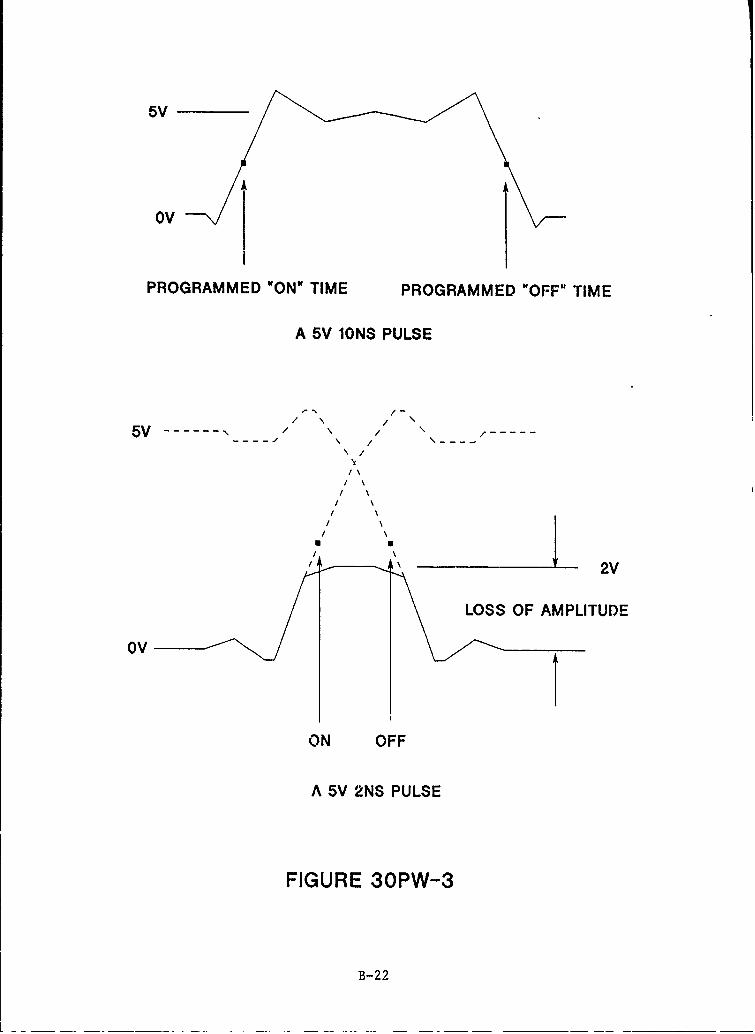
5V
ov
PROGRAMMED "ON" TIME PROGRAMMED wOFF" TIME
A 5V iONS PULSE
5V ------
A 5 2SPUS
FIGURE 3OPW-3
B-22

Appendix C
Proposed Requirements to Qualify CAD Tools
for
VHSIC/VLSI Devices

1. Generic Plan
This Qualification plan is applicable to all software Computer Aided DA.velopmental(CA. "used in the VHSIC design process being Qualified. Since, all CAD Tools covered in this C.Plan are used in the design methodology of VIiSIC devices and the Design Organizsd-r. ,zon'tls thedesign methodology. the c9ntrol of CAD Tools Is placed with the Design Organizatia.
Thi. plan treats each tool as a Black Box, i.e., the major interest is Input to the tool %nd output fromtbe toot. Fow the tool processes the input to produce its output is of minor concern. Any majordeviat!in Eom this philosophy would greatly inhibit the development and placement of new and-npred tools and would not allow for differences in the environment of the various VHSIC Processes.
,- Black Box methodology will reduce the reluctance of a tool's vendor to qualify for proprietyreaseos. reduce the knowledge needed to qualify a tool and reduce the time to qualify a tool.
2. Steps to Qualify CAD Tools1. A CAD Tool List must be submined to the Qualifying Organization.
2. A Tool Fucncn List must be submitted to the Qualifying Organization for each Qu 'ing2 Tool.
3. A Tool Dependency List must be submitted to the Qua.Ufying Orgar.ization for .ach Quaib..M.Tool.
.4. A Qualification Plan must be developed for each Tool ,Lnd submitted to te QualifyingO:Sanizadon.
5. Each Tool must meet the Qualification objectives stated in its Qualification Plan.
6. The Archiving Facility must be Qualified.
3. CAD Tool ListIt is the Design Organizations responsibility to prepare a ccnp.2 , list of all CAD tools used in the
VHSIC factty to be qualfled. the CAD Trol Li:t . !t iL a-sune. that the overall responsibility for theVHSIC design and production will reside with the Design Oranizadon an. the owner of the VHSICproduction facilities will be considered as a sub-contractor. T,":s list shall include:
I. the tool name.
C-I

2. the version currently being used.
3. the date this version was installed,
4. the identity of the installer,
S. the date the tool was quafed,
6. a short description of the tools purpose,
7. tool sponsor.Each tool must have a sponsor, a person who is responsible for the tool in the Design Organizaionsfacility. The name of the tool's sponsor must be entered on the CAD Tool List . The CAD Tooi Listmust be available to the Qualifying personnel before Qualification begins. If a tool has not beenQualifed, then the qualification date is blank.
As a new version of the tool is installed for execution, the following must be added to the CADTool Lr :
1. the tool name.
2. the version number,
3. the date of instalation,
4. the identity of the Installer
S. the date the version is Qualified,
6. the tool sponsor.If a tool has not been Qualifled, then the qualification date is blank.
If a waver has been granted for a Tool, then the following must be added to the CAD Tool Lis:
1. Tool name,
2. Tool version number.
3. Tool sponsor.
4. type of waverReliability, Qualificaton or Archlve Facility),
5. date waver is approved.
6. date waver expires,
7. name of the Qualification Organizanon person who approved the waver,
8. a short re-son for the waver request.
All data on tle CAD Too! List must b'e Cur-ent.
4. Tool Function ListEach Tool must have an official minimum set list of Functions, Tool Ftncrion List. For the
purpose here. if a mi imum function is omitted. then the user can not perform the foo the tool wasdesigned to do. Only minimal functions are included in te specification: i.e., the word function meansminimal function for ah document unless specified. It is the Design Organizations responsib.iiy zoproduce and verify the Tool Funcnon List for each tool. It is the responsibility of the vendor ci thetool to provide methocs to verify that each function operates as expected as described in theaccompanying documentation of the tool (see Documentation). The Tool Func~ion List must have:
I. Tool name.
2. version number,
C-2
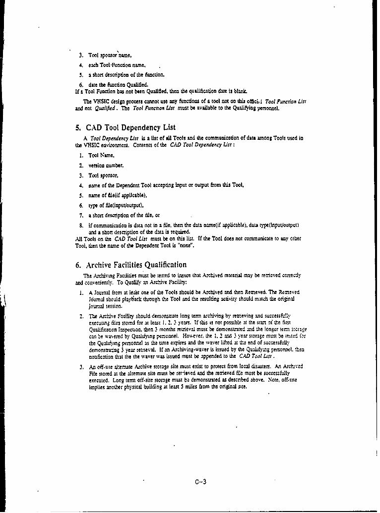
3. Toot sponsor 1omnme,
4. each Tool-uN-ctiou name,
5. a short description of the function,
6. date the function Qualied.If a Tool Function has niot been Qualified, then the qualication date is blank,
The VHSIC design process cannot use ay 6NtctiOUs Of a to ol not on this ofdci, I Tool Function Listand not Qualified. The Tool Funcuion List must be available to the Qualifying personnel.
5. CAD Tool Dependency ListA Tool Dependency Lir is a list of all Tools and the communicadon of data among Tools used in
the VHSIC enivironmient. Contents of the CAD Tool Dependency List:
1. Tool N~ame.
2. version number,
3. Tool sponsor,
4. name of the Dependent Tool accepting Input or output from this Tool,
5. name of &ile(if applicable),
6. type of file(input/output).
7. a short description of the Mie, or
8. if comnmunication is data not in a fie, then the data narne(if applicable), data type(lInput/output)vad a short detscription of the data is required.
All Tools on the CAD Tool List must be on this list, 'If the Tool does not communicate to any etherTool, then the name of the Dependent Tool is "none".
6. Archive Facilities QualificationThe A.-chivig Facilities must be tested to insur-e that A~chived matenial may be retioved ccrre 'Jy
and cotiverientgy. To Qualify an Archive Facility:
1. A Journal frcm at least one of the Tools should be Archived and then Retrieved. The RernevedJournal should play :ick thmugh the Toot and the resulting acdtityv should match the originaljournal session.
2.Tla Arzhive Facility should demonstrate lona term wrchi~ing by retrievingt and succesf.!lvexecuting dIe-s stored for at least 1. 2. 3 years. If this is not possible at te stars of the firstQua U-.catucn inspection, then 3 months retieva must be demonstrated 2nd :he !ons-er tern s-cragecan be wavered by Qualiying personniel. Ho'~ever. the 1. 2 and 3 ysar storage must be tetcd (-nthe Qualifying personnel as &h tie expires and the waver lifted at the end of successfuliydemonstra tng 3 year retrieval. If an Archiving-waver is issued by the Quaifytrig& personnel. thenOonfication that the the waver was issued must be appended to the CAD Tool List.
3. An off-site alternate Archive storase site must exist to protect from local disasters. AnArh.dRie stored at the alternate site must be ret-eved and the retrieved file must be succes3fiallyexecuted. Lora term off-site storage must ba demonstrated as descr.bed above. Note. off-siteimplies another physical building at least 5 miiles from the original site.
c-3

7. CAD Tool Qualification PlanIt is the Vendor of the tools responsibility to provide a detailed plan to demonstrate the corecmess
and capsbility cf the tool, CAD Tool Quolification Plan. The plan should include the input to the tool.its output or action =d methods of verifying the correctness of the output or sction for each utioction onthe Tool Function List. The capability of the tool must be demonstrated,
7.1 Vendor of the Tool
The Vendor of the tool is normally the organization or its representative who developed the so',arefor the CAD Tool. However, the Design Organization has the ultimate responsibility of adhering to theVHSIC CAD Tool Qualification Plan. The word Design Organization may be substituted for he wo:dVendor throughout this document.
7.2 Verifying Correctness of a Tool FunctionA Tool Fucotin Is considered correct when the documented input produces the desired results or
actions, and further, the results or actions match those described in the documentation of the tool.
7.3 Demonstrating Capability of a Tool FunctionA Tool Function has demonsmated Capability when It is able to process VHSIC circuits near the
maximum complexity processed in the VHSIC Line being Qualified and when the tnie and cost of theprocessing is within the Indust'y norm for the Tool Function.
8. Tools Version identityThe release version Identity of the tool is the responsibility of the Vendor of the Tool. It is the Tool
Vendors responsibility to designate major or minor changes to the tool. Each addidonal in.ttallati:n ofthe tool in the VHSIC facility other than a copy must have a new identifying version number. 7h..eieversion numbers should be in ascendtng sequence; major ad minor version numbers must be dtentned
8.1 Current Version
The current version of a tool is the version executing in the Qualified VHSIC facility and is '.sed todevelop the devics in the facility. Normally. this would be the last Qualified version listed -n ±.CAD Too! List.
8.2 Compatibthiy of Sofr'Aare Release Versions
All subsequent versions of a software tool must zdcept the previous versions iCput.Ve.s.cnCompatibility. This should be .t of the tool butmay be furnushed by a stand.alone so.varetranslat;on system. A new verstcn of a tool should provide the critical functions of the previous :e.sion.and. a new version should accept and execute the Journal File (see Human Entry secton) of theprevious version. This provides a method of restrng the accuracy of the new version to the stardards ofthe previous version.
9. Tool Input9.1 Human Entry
For each tool, all human entered data must be captured by the machine run.nng the tool in a Rile orfiles that are saved or .Archived(see Archive Files section). This Archived File or Files is called a
c-4

Journal File because it is a record of all human data entered during the session the tool was run. ThisJournal File must be formatted in a human readable or convertible to a human readable format via a,machine resident translating system. Further, the tool must be able to read this archived data Journal inplace of the human entry and execute the commands In the Journal File as if the commands were humanentered, Playback. As new versions of the tool become available, this journaling and playbackcapability is used to qualify the new version against the standard of the old version. Note; the humanreadable requirement is designed to provide portability and thus not be dependent on hardware orversions of software(host operating system and/or the tools system).
9.2 Machine Entvy
If a tool's input is from another tooltool-to.tool communication, then the input must be verifiableand specifications exist decribing its format. The responsibility to verify the correcmess of the tool.to.tool communication resides with the vendor introducing the new version or tool. If tool A outputs data
that tool B uses as input; then, if tool A introduces a new version or tool, the vendor of tool A isresponsible for the verification. The reverse is also true; tool A output is input to tool B and vendor oftool B introduces a new version or tool, the vendor of tool B is responsible for verlficaton that tool Bcorrectly interprets the input from tool A. (See also CAD Tool Dependency List section.)
9.3 Tools Response 'to Data
The Tool's Software should produce good results for test data without aborting when an abort is notthe desired result. When an abort Is expected as part of the test data, then comprehensible errormessages should be generated. All error messages should be understandable to a normal user of thetool.
9.4 Verification of Input
Verification of input requues that given the input meets documented standards, then, the tool reactsas expec:ted judged against its documentation.
10. Tool Output
The ouTput or acton of each function in .he tool must be verifiable. either by building the device andobserving its operation or by captunng computer output and demonstratng ts corrctness or by emaringdocumented input and observing the action against documented action. T"he vendor of the tool isresponsible to provide methods to demonstrate the correctness of the output or action.
10 1 Output Format
A %n;vren spe::icancn must exist descnbing the format of aUl output that exists after a tools sesicnis ended kperm-n: output). This includes data that is used by the tool to continue from sessiontc-session. The ou.ou; must be capable of be-rig archaved and all environm.-ntal parameters affecutn rheoperauon of the :col. including date stamping, must be included in the archived file(see Archive Fi1e!).All arch:vable output must be in human readable form or a trar.slator exist :o convert the output to thatform. An excepucn to the human readable condition can be made when '.he output is tn an indus.r" orgovernment azcepted standard format.
10.1.1 Archive Files
All Archived Files must be labeled so that all environmental parameters effecting the output oraction of the tool may be identied(time, date.session. tool, tool version. Machine and Machineoperadi system, etc.). Archived Files imply that the files are stored for at least the length of thecontract and may be retrieved %ithin a reasonable time in the same state as when archived. The
c-5

Archiving Facilities must be Qualified.
11. DocumentationAll supporting documentation must be complete and current with the tool's current version number
and specify the version number oeing supported. It must specify the input and the expected action oroutput of all functions. All archivable output(non.temporary dles) must be described in thedocumentation. A temporary file Is one that only exists during the execution of the tool and need not bedocumented. To verify that documentation Is correct, the documented input to a function is entered andthe resulting output or action must match the description of the results recorded In the documentation. Ifthe match does not occur, then either the software or documentation must be changed by the vendorbefore the Tool can be Qualifed and the function must be Requalified. All functions must be Qualified:where this is not possible, then the percentage of coverage must be documented. The coverage must beequjl or above industry norm for this VHSIC environment.
12. Testing ModelsVWbere appropriate each software tool should be tested with a set of approved models of various
slzes(cell, macro, subchip and chips of at least 2 sizes) to test each product for correcmess andcapability. One of the chips should be of small to moderate size to check correctness and the othershould be a large chip, as bounded by the maximum size chip produced in the V-SIC facility, to checkcapability of the tool to process large jobs in reasonable time and cost. Reasonableness may be judgedagainst Industry norms for this tool and function. Where models ar not appropriate, then the vendor ofthe tool must provide a method to verify the output of the tool for correctness and capability(seeCorrectness and Capability sections).
13. Reliability or Quality QualificationThe reliability of the tool must be documented. The measure or Figure of Merit for Quality :.; the
number of Severe Faults (see Severe Fault section) per 1000 lines of non.commented code. A T.olQualifies for Quality by showing that the Quality Figure of Merit or some function of thb Fliu:e ofMerit is either stable or decremsing in time using standard statistical methodology. This Figure .ot Meatshould be below the median figure for all software released in the United S:ates.
If a new version of the tool is released. then previous rellabdity data may be applied to the r.-wrelease if the vendor of the tool has demostrated reliability at revisions.
13.1 Severe Fault
13.1.1 Fault
A Fault is a deviaton of specified action from documented action gien specifed dcurleo:ed WCu:.
13.1.2 Severe Fault
A Severe Fault is a fault that prevents the user from pOrforming the func.ion or executing '.h. 0o1for which there is no convenient work.around.
13.1.3 Work.around
A work.around is a substitute set of actions oi functions e.ecuting under the tool that executes afunction working incorrectly or not working at all to produce correct results.
c-6

The standard cel symbols should correctly match the library symbols used In the VHSIC environment.The symbol layout displayed by the Tool should be true to the nedist produced by the Tool. Since theSchematic Capture System normally interacts with simulation and layout tools, then the netlist fileshould be tested for input compadblty with the interacting tools. All functions on the Tool FuncdonLst should be tested for correctness,
17.2 Predictive or Simulation Tools
To qualify a Simulation Tool, real VHSIC devices should be simulated and the simulated devicesshould be built in the VHSIC environment being Qualified. The observed behavior of the verifyingdevices should not be statistically different from its simulated behavior or the difference betweensimulated and observed behavior should be below the Industry norm for the VHSIC environment. ifIndusty norms are used to judge the differences between simulated and observed behavior, then thenorms should be documented before Qualifying sessions are started.
17.3 Design Rules Checkers
Design Rules Checkers are software systems designed to audit the description of the circuit against aset of prescribed rules. On tools that are rules checkers, test cases should be available to prove that thetool is correctly rejecdngthose designs that deviate from the rules and accepting those designs that arewithin the rules.. All rules should be verified.
17.4 Routing SystemsA Routing System is a software tool that makes the physical electrical connections between the
primitive elements of a VHSIC design placed in the Silicon matrix usually to some design cnterion.The automatic routing system should cover at least 9951 of the design. The automatic routing systemshould have some method of specifying and handling critical paths. If the routing system handles mult.metal technologies, then power and ground paths should be restrictable to a single metal level. Aninteractive router should exist to provide special manual intervention to customize portions of theautomatic routers output. The output of the automatic and interactive routers should be compauble. Theinteractive router should be able to read and manipulate the data-ba.,.e of the automatc router. A ne-liRor connectivity cbeck should be available to show that the router system has completed its functio;uwhile maintaning the original con.ectivity of the specified circuit. A test should exist to show that -heelectrical(shorts and opens) and logic functions of the original specified circuit have not been violated.A test should e.dst to show that the design rules for the mask producing methodologey have not beenviolated.
17.5 Mask GeneratorsA Mask Cenera:or is a software tool that produces a file of commands that dnvts equipme.: to
produce the mask set for the VHSIC device given some aeomenc descnption of the VHSIC ,,.'eFor Mask Generators. an extractor should exist that extracts a net.list from the geometry produced bythe Generator to show that proper connectaity has been established. A test should exist to show that theelectrical(shorts and opens) and logic functions of the original specified circuit have not been violated.Some method should ex:st to show that the Generator does not violate the mask producing methcdolog.rules.
17.6 Silicon CompilersA Silicon Compiler is a software tool that produces a file of commands that drives -equipment to
produce the mask set for the VHSIC device given some higher language description of the VHSICdevice. Silicon Compilers should produce output that is within the design rules for the productionenvironment it is used in ard its output is expected to pass the Design Rules Checker for the productionenvironment. An extractor should exist to reformat the output of the Silicon Compiler to prove that the
C-7

Silicon Compiler did produce the circuit that was entered, functionally, logically and electrically(noshorts or opens). Some method should exist to show that the Compiler d es not violate the ms.skproducing methodology rules for the VHSIC environment being Quali..,d.
17.7 Other ToolsTools not specifically discussed in the section should be qualified In the following generic manner
1. The Tool Function List should be examined against the Tool Qual(fying Plan to Insure that allfunctions are included in the pla.
2. The Tool Dependenc}-; List should be examined against the Tool Qualifylng Plan to insure thatall tool communication dependencies are tested.
3. The Tool Qualiffing Plan should be examined for completeness. reasonableness and is withinldustry norms for the Tool type wd VNSIC environment.
4. The Journaling and Playbeck functions should be tested against Documentation.
5. Al Permanent Fles should be tested against documented format requirements.
C-8


![API 2W [1993]](https://img.dokumen.tips/doc/110x75/577cd4db1a28ab9e78994d52/api-2w-1993.jpg)