Embed Size (px)
Citation preview

1FEATURES
1
2
3
4
5
6
7
8
16
15
14
13
12
11
10
9
A/B1A1B1Y2A2B2Y
GND
VCC
OE4A4B4Y3A3B3Y
D OR PW PACKAGE(TOP VIEW)
DESCRIPTION/ORDERING INFORMATION
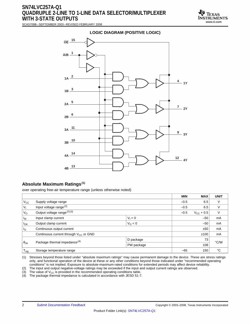
SN74LVC257A-Q1QUADRUPLE 2-LINE TO 1-LINE DATA SELECTOR/MULTIPLEXER
WITH 3-STATE OUTPUTSSCAS709B–SEPTEMBER 2003–REVISED FEBRUARY 2008
www.ti.com
• Qualified for Automotive Applications• ESD Protection Exceeds 2000 V Per
MIL-STD-883, Method 3015; Exceeds 200 VUsing Machine Model (C = 200 pF, R = 0)
• Operates From 2 V to 3.6 V• Inputs Accept Voltages to 5.5 V• Max tpd of 4.6 ns at 3.3 V• Typical VOLP (Output Ground Bounce) < 0.8 V
at VCC = 3.3 V, TA = 25°C• Typical VOHV (Output VOH Undershoot) > 2 V
at VCC = 3.3 V, TA = 25°C
The SN74LVC257A quadruple 2-line to 1-line data selector/multiplexer is designed for 2.7-V to 3.6-V VCCoperation.
The device is designed to multiplex signals from 4-bit data sources to 4-output data lines in bus-organizedsystems. The 3-state outputs do not load the data lines when the output-enable (OE) input is at a high logic level.
Inputs can be driven from either 3.3-V or 5-V devices. This feature allows the use of this device as a translator ina mixed 3.3-V/5-V system environment.
To ensure the high-impedance state during power up or power down, OE should be tied to VCC through a pullupresistor; the minimum value of the resistor is determined by the current-sinking capability of the driver.
ORDERING INFORMATION (1)
TA PACKAGE (2) ORDERABLE PART NUMBER TOP-SIDE MARKINGSOIC – D Reel of 2500 SN74LVC257AQDRQ1 L257AQ1
–40°C to 125°CTSSOP – PW Reel of 2000 SN74LVC257AQPWRQ1 L257AQ1
(1) For the most current package and ordering information, see the Package Option Addendum at the end of this document, or see the TIweb site at www.ti.com.
(2) Package drawings, thermal data, and symbolization are available at www.ti.com/packaging.
FUNCTION TABLEINPUTS OUTPUT
YOE A/B A BH X X X ZL L L X LL L H X HL H X L LL H X H H
1
Please be aware that an important notice concerning availability, standard warranty, and use in critical applications ofTexas Instruments semiconductor products and disclaimers thereto appears at the end of this data sheet.
PRODUCTION DATA information is current as of publication date. Copyright © 2003–2008, Texas Instruments IncorporatedProducts conform to specifications per the terms of the TexasInstruments standard warranty. Production processing does notnecessarily include testing of all parameters.
www.ti.com
4Y
3Y
2Y
1Y
A/B
OE
4B
4A
3B
3A
2B
2A
1B
1A4
2
3
75
6
911
10
1214
13
1
15
Absolute Maximum Ratings (1)
SN74LVC257A-Q1QUADRUPLE 2-LINE TO 1-LINE DATA SELECTOR/MULTIPLEXERWITH 3-STATE OUTPUTSSCAS709B–SEPTEMBER 2003–REVISED FEBRUARY 2008
LOGIC DIAGRAM (POSITIVE LOGIC)
over operating free-air temperature range (unless otherwise noted)
MIN MAX UNITVCC Supply voltage range –0.5 6.5 VVI Input voltage range (2) –0.5 6.5 VVO Output voltage range (2) (3) –0.5 VCC + 0.5 VIIK Input clamp current VI < 0 –50 mAIOK Output clamp current VO < 0 –50 mAIO Continuous output current ±50 mA
Continuous current through VCC or GND ±100 mAD package 73
θJA Package thermal impedance (4) °C/WPW package 108
Tstg Storage temperature range –65 150 °C
(1) Stresses beyond those listed under "absolute maximum ratings" may cause permanent damage to the device. These are stress ratingsonly, and functional operation of the device at these or any other conditions beyond those indicated under "recommended operatingconditions" is not implied. Exposure to absolute-maximum-rated conditions for extended periods may affect device reliability.
(2) The input and output negative-voltage ratings may be exceeded if the input and output current ratings are observed.(3) The value of VCC is provided in the recommended operating conditions table.(4) The package thermal impedance is calculated in accordance with JESD 51-7.
2 Submit Documentation Feedback Copyright © 2003–2008, Texas Instruments Incorporated
Product Folder Link(s): SN74LVC257A-Q1

www.ti.com
Recommended Operating Conditions (1)
Electrical Characteristics
SN74LVC257A-Q1QUADRUPLE 2-LINE TO 1-LINE DATA SELECTOR/MULTIPLEXER
WITH 3-STATE OUTPUTSSCAS709B–SEPTEMBER 2003–REVISED FEBRUARY 2008
MIN MAX UNITOperating 2 3.6
VCC Supply voltage VData retention only 1.5
VIH High-level input voltage VCC = 2.7 V to 3.6 V 2 VVIL Low-level input voltage VCC = 2.7 V to 3.6 V 0.8 VVI Input voltage 0 5.5 VVO Output voltage 0 VCC V
VCC = 2.7 V –12IOH High-level output current mA
VCC = 3 V –24VCC = 2.7 V 12
IOL Low-level output current mAVCC = 3 V 24
Δt/Δv Input transition rise or fall rate 10 ns/VTA Operating free-air temperature –40 125 °C
(1) All unused inputs of the device must be held at VCC or GND to ensure proper device operation. Refer to the TI application report,Implications of Slow or Floating CMOS Inputs, literature number SCBA004.
over recommended operating free-air temperature range (unless otherwise noted)
PARAMETER TEST CONDITIONS VCC MIN TYP (1) MAX UNITIOH = –100 µA 2.7 V to 3.6 V VCC – 0.2
2.7 V 2.2VOH IOH = –12 mA V
3 V 2.4IOH = –24 mA 3 V 2.2IOL = 100 µA 2.7 V to 3.6 V 0.2
VOL IOL = 12 mA 2.7 V 0.4 VIOL = 24 mA 3 V 0.55
II VI = 5.5 V or GND 3.6 V ±5 µAIOZ VO = VCC or GND 3.6 V ±15 µAICC VI = VCC or GND, IO = 0 3.6 V 10 µAΔICC One input at VCC – 0.6 V, Other inputs at VCC or GND 2.7 V to 3.6 V 500 µA
Ci VI = VCC or GND 3.3 V 5 pFCo VO = VCC or GND 3.3 V 5 pF
(1) All typical values are at VCC = 3.3 V, TA = 25°C.
Copyright © 2003–2008, Texas Instruments Incorporated Submit Documentation Feedback 3
Product Folder Link(s): SN74LVC257A-Q1

www.ti.com
Switching Characteristics
Operating Characteristics
SN74LVC257A-Q1QUADRUPLE 2-LINE TO 1-LINE DATA SELECTOR/MULTIPLEXERWITH 3-STATE OUTPUTSSCAS709B–SEPTEMBER 2003–REVISED FEBRUARY 2008
over recommended operating free-air temperature range (unless otherwise noted) (see Figure 1)
VCC = 3.3 VVCC = 2.7 VFROM TO ± 0.3 VPARAMETER UNIT(INPUT) (OUTPUT)MIN MAX MIN MAX
A or B 5.4 1 4.6tpd Y ns
A/B 7.5 1 6.4ten OE Y 6.7 1 5.6 nstdis OE Y 4.7 0.5 4.3 ns
tsk(o) 1 ns
TA = 25°C
VCC = 2.5 V VCC = 3.3 VTESTPARAMETER UNITCONDITIONS TYP TYPCpd Power dissipation capacitance f = 10 MHz 14.5 15.5 pF
4 Submit Documentation Feedback Copyright © 2003–2008, Texas Instruments Incorporated
Product Folder Link(s): SN74LVC257A-Q1
www.ti.com
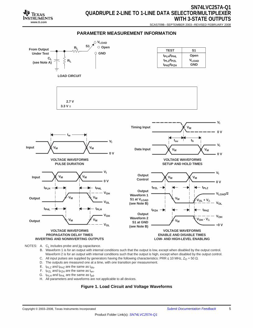
PARAMETER MEASUREMENT INFORMATION
VM
thtsu
From OutputUnder Test
CL(see Note A)
LOAD CIRCUIT
S1VLOAD
Open
GND
RL
RL
Data Input
Timing InputVI
0 V
VI
0 V0 V
tw
Input
VOLTAGE WAVEFORMSSETUP AND HOLD TIMES
VOLTAGE WAVEFORMSPROPAGATION DELAY TIMES
INVERTING AND NONINVERTING OUTPUTS
VOLTAGE WAVEFORMSPULSE DURATION
tPLH
tPHL
tPHL
tPLH
VOH
VOH
VOL
VOL
VI
0 VInput
OutputWaveform 1S1 at VLOAD(see Note B)
OutputWaveform 2
S1 at GND(see Note B)
VOL
VOH
tPZL
tPZH
tPLZ
tPHZ
VLOAD/2
0 V
VOL + V∆
VOH - V∆
≈0 V
VI
VOLTAGE WAVEFORMSENABLE AND DISABLE TIMES
LOW- AND HIGH-LEVEL ENABLING
Output
Output
tPLH/tPHLtPLZ/tPZLtPHZ/tPZH
OpenVLOADGND
TEST S1
NOTES: A. CL includes probe and jig capacitance.B. Waveform 1 is for an output with internal conditions such that the output is low, except when disabled by the output control.
Waveform 2 is for an output with internal conditions such that the output is high, except when disabled by the output control.C. All input pulses are supplied by generators having the following characteristics: PRR ≤ 10 MHz, ZO = 50 Ω.D. The outputs are measured one at a time, with one transition per measurement.E. tPLZ and tPHZ are the same as tdis.F. tPZL and tPZH are the same as ten.G. tPLH and tPHL are the same as tpd.H. All parameters and waveforms are not applicable to all devices.
OutputControl
VM VM
VM VM
VM VM
VM
VM VM
VM
VM
VM
VI
VM
VM
2.7 V3.3 V ± 0.3 V
500 Ω500 Ω
VCC RL
6 V6 V
VLOAD CL
50 pF50 pF
0.3 V0.3 V
V∆
2.7 V2.7 V
VI
1.5 V1.5 V
VMtr/tf
≤2.5 ns≤2.5 ns
INPUTS
SN74LVC257A-Q1QUADRUPLE 2-LINE TO 1-LINE DATA SELECTOR/MULTIPLEXER
WITH 3-STATE OUTPUTSSCAS709B–SEPTEMBER 2003–REVISED FEBRUARY 2008
Figure 1. Load Circuit and Voltage Waveforms
Copyright © 2003–2008, Texas Instruments Incorporated Submit Documentation Feedback 5
Product Folder Link(s): SN74LVC257A-Q1

PACKAGE OPTION ADDENDUM
www.ti.com 10-Dec-2020
Addendum-Page 1
PACKAGING INFORMATION
Orderable Device Status(1)
Package Type PackageDrawing
Pins PackageQty
Eco Plan(2)
Lead finish/Ball material
(6)
MSL Peak Temp(3)
Op Temp (°C) Device Marking(4/5)
Samples
CLVC257AQPWRG4Q1 ACTIVE TSSOP PW 16 2000 RoHS & Green NIPDAU Level-1-260C-UNLIM -40 to 125 L257AQ1
SN74LVC257AQDRG4Q1 ACTIVE SOIC D 16 2500 RoHS & Green NIPDAU Level-1-260C-UNLIM -40 to 125 L257AQ1
(1) The marketing status values are defined as follows:ACTIVE: Product device recommended for new designs.LIFEBUY: TI has announced that the device will be discontinued, and a lifetime-buy period is in effect.NRND: Not recommended for new designs. Device is in production to support existing customers, but TI does not recommend using this part in a new design.PREVIEW: Device has been announced but is not in production. Samples may or may not be available.OBSOLETE: TI has discontinued the production of the device.
(2) RoHS: TI defines "RoHS" to mean semiconductor products that are compliant with the current EU RoHS requirements for all 10 RoHS substances, including the requirement that RoHS substancedo not exceed 0.1% by weight in homogeneous materials. Where designed to be soldered at high temperatures, "RoHS" products are suitable for use in specified lead-free processes. TI mayreference these types of products as "Pb-Free".RoHS Exempt: TI defines "RoHS Exempt" to mean products that contain lead but are compliant with EU RoHS pursuant to a specific EU RoHS exemption.Green: TI defines "Green" to mean the content of Chlorine (Cl) and Bromine (Br) based flame retardants meet JS709B low halogen requirements of <=1000ppm threshold. Antimony trioxide basedflame retardants must also meet the <=1000ppm threshold requirement.
(3) MSL, Peak Temp. - The Moisture Sensitivity Level rating according to the JEDEC industry standard classifications, and peak solder temperature.
(4) There may be additional marking, which relates to the logo, the lot trace code information, or the environmental category on the device.
(5) Multiple Device Markings will be inside parentheses. Only one Device Marking contained in parentheses and separated by a "~" will appear on a device. If a line is indented then it is a continuationof the previous line and the two combined represent the entire Device Marking for that device.
(6) Lead finish/Ball material - Orderable Devices may have multiple material finish options. Finish options are separated by a vertical ruled line. Lead finish/Ball material values may wrap to twolines if the finish value exceeds the maximum column width.
Important Information and Disclaimer:The information provided on this page represents TI's knowledge and belief as of the date that it is provided. TI bases its knowledge and belief on informationprovided by third parties, and makes no representation or warranty as to the accuracy of such information. Efforts are underway to better integrate information from third parties. TI has taken andcontinues to take reasonable steps to provide representative and accurate information but may not have conducted destructive testing or chemical analysis on incoming materials and chemicals.TI and TI suppliers consider certain information to be proprietary, and thus CAS numbers and other limited information may not be available for release.
In no event shall TI's liability arising out of such information exceed the total purchase price of the TI part(s) at issue in this document sold by TI to Customer on an annual basis.

PACKAGE OPTION ADDENDUM
www.ti.com 10-Dec-2020
Addendum-Page 2
OTHER QUALIFIED VERSIONS OF SN74LVC257A-Q1 :
• Catalog: SN74LVC257A
• Enhanced Product: SN74LVC257A-EP
• Military: SN54LVC257A
NOTE: Qualified Version Definitions:
• Catalog - TI's standard catalog product
• Enhanced Product - Supports Defense, Aerospace and Medical Applications
• Military - QML certified for Military and Defense Applications

TAPE AND REEL INFORMATION
*All dimensions are nominal
Device PackageType
PackageDrawing
Pins SPQ ReelDiameter
(mm)
ReelWidth
W1 (mm)
A0(mm)
B0(mm)
K0(mm)
P1(mm)
W(mm)
Pin1Quadrant
CLVC257AQPWRG4Q1 TSSOP PW 16 2000 330.0 12.4 6.9 5.6 1.6 8.0 12.0 Q1
PACKAGE MATERIALS INFORMATION
www.ti.com 16-Oct-2020
Pack Materials-Page 1

*All dimensions are nominal
Device Package Type Package Drawing Pins SPQ Length (mm) Width (mm) Height (mm)
CLVC257AQPWRG4Q1 TSSOP PW 16 2000 853.0 449.0 35.0
PACKAGE MATERIALS INFORMATION
www.ti.com 16-Oct-2020
Pack Materials-Page 2


www.ti.com
PACKAGE OUTLINE
C
14X 0.65
2X4.55
16X 0.300.19
TYP6.66.2
1.2 MAX
0.150.05
0.25GAGE PLANE
-80
BNOTE 4
4.54.3
A
NOTE 3
5.14.9
0.750.50
(0.15) TYP
TSSOP - 1.2 mm max heightPW0016ASMALL OUTLINE PACKAGE
4220204/A 02/2017
1
89
16
0.1 C A B
PIN 1 INDEX AREA
SEE DETAIL A
0.1 C
NOTES: 1. All linear dimensions are in millimeters. Any dimensions in parenthesis are for reference only. Dimensioning and tolerancing per ASME Y14.5M. 2. This drawing is subject to change without notice. 3. This dimension does not include mold flash, protrusions, or gate burrs. Mold flash, protrusions, or gate burrs shall not exceed 0.15 mm per side. 4. This dimension does not include interlead flash. Interlead flash shall not exceed 0.25 mm per side.5. Reference JEDEC registration MO-153.
SEATINGPLANE
A 20DETAIL ATYPICAL
SCALE 2.500
www.ti.com
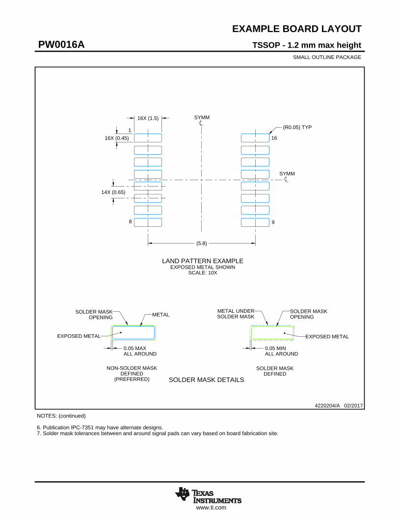
EXAMPLE BOARD LAYOUT
0.05 MAXALL AROUND
0.05 MINALL AROUND
16X (1.5)
16X (0.45)
14X (0.65)
(5.8)
(R0.05) TYP
TSSOP - 1.2 mm max heightPW0016ASMALL OUTLINE PACKAGE
4220204/A 02/2017
NOTES: (continued) 6. Publication IPC-7351 may have alternate designs. 7. Solder mask tolerances between and around signal pads can vary based on board fabrication site.
LAND PATTERN EXAMPLEEXPOSED METAL SHOWN
SCALE: 10X
SYMM
SYMM
1
8 9
16
15.000
METALSOLDER MASKOPENING
METAL UNDERSOLDER MASK
SOLDER MASKOPENING
EXPOSED METALEXPOSED METAL
SOLDER MASK DETAILS
NON-SOLDER MASKDEFINED
(PREFERRED)
SOLDER MASKDEFINED

www.ti.com
EXAMPLE STENCIL DESIGN
16X (1.5)
16X (0.45)
14X (0.65)
(5.8)
(R0.05) TYP
TSSOP - 1.2 mm max heightPW0016ASMALL OUTLINE PACKAGE
4220204/A 02/2017
NOTES: (continued) 8. Laser cutting apertures with trapezoidal walls and rounded corners may offer better paste release. IPC-7525 may have alternate design recommendations. 9. Board assembly site may have different recommendations for stencil design.
SOLDER PASTE EXAMPLEBASED ON 0.125 mm THICK STENCIL
SCALE: 10X
SYMM
SYMM
1
8 9
16

IMPORTANT NOTICE AND DISCLAIMER
TI PROVIDES TECHNICAL AND RELIABILITY DATA (INCLUDING DATASHEETS), DESIGN RESOURCES (INCLUDING REFERENCE DESIGNS), APPLICATION OR OTHER DESIGN ADVICE, WEB TOOLS, SAFETY INFORMATION, AND OTHER RESOURCES “AS IS” AND WITH ALL FAULTS, AND DISCLAIMS ALL WARRANTIES, EXPRESS AND IMPLIED, INCLUDING WITHOUT LIMITATION ANY IMPLIED WARRANTIES OF MERCHANTABILITY, FITNESS FOR A PARTICULAR PURPOSE OR NON-INFRINGEMENT OF THIRD PARTY INTELLECTUAL PROPERTY RIGHTS.These resources are intended for skilled developers designing with TI products. You are solely responsible for (1) selecting the appropriate TI products for your application, (2) designing, validating and testing your application, and (3) ensuring your application meets applicable standards, and any other safety, security, or other requirements. These resources are subject to change without notice. TI grants you permission to use these resources only for development of an application that uses the TI products described in the resource. Other reproduction and display of these resources is prohibited. No license is granted to any other TI intellectual property right or to any third party intellectual property right. TI disclaims responsibility for, and you will fully indemnify TI and its representatives against, any claims, damages, costs, losses, and liabilities arising out of your use of these resources.TI’s products are provided subject to TI’s Terms of Sale (www.ti.com/legal/termsofsale.html) or other applicable terms available either on ti.com or provided in conjunction with such TI products. TI’s provision of these resources does not expand or otherwise alter TI’s applicable warranties or warranty disclaimers for TI products.
Mailing Address: Texas Instruments, Post Office Box 655303, Dallas, Texas 75265Copyright © 2020, Texas Instruments Incorporated