Embed Size (px)
Citation preview
Optone Technology Limited
http://www.optone.net
QSFP+ Series
1/11
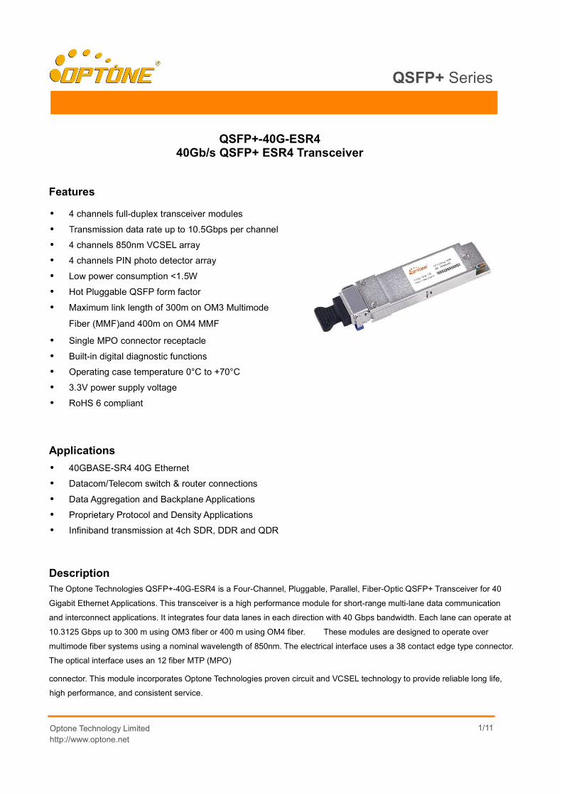
QSFP+-40G-ESR4
40Gb/s QSFP+ ESR4 Transceiver
Features
� 4 channels full-duplex transceiver modules
� Transmission data rate up to 10.5Gbps per channel
� 4 channels 850nm VCSEL array
� 4 channels PIN photo detector array
� Low power consumption <1.5W
� Hot Pluggable QSFP form factor
� Maximum link length of 300m on OM3 Multimode
Fiber (MMF)and 400m on OM4 MMF
� Single MPO connector receptacle
� Built-in digital diagnostic functions
� Operating case temperature 0°C to +70°C
� 3.3V power supply voltage
� RoHS 6 compliant
Applications
� 40GBASE-SR4 40G Ethernet
� Datacom/Telecom switch & router connections
� Data Aggregation and Backplane Applications
� Proprietary Protocol and Density Applications
� Infiniband transmission at 4ch SDR, DDR and QDR
Description
The Optone Technologies QSFP+-40G-ESR4 is a Four-Channel, Pluggable, Parallel, Fiber-Optic QSFP+ Transceiver for 40
Gigabit Ethernet Applications. This transceiver is a high performance module for short-range multi-lane data communication
and interconnect applications. It integrates four data lanes in each direction with 40 Gbps bandwidth. Each lane can operate at
10.3125 Gbps up to 300 m using OM3 fiber or 400 m using OM4 fiber. These modules are designed to operate over
multimode fiber systems using a nominal wavelength of 850nm. The electrical interface uses a 38 contact edge type connector.
The optical interface uses an 12 fiber MTP (MPO)
connector. This module incorporates Optone Technologies proven circuit and VCSEL technology to provide reliable long life,
high performance, and consistent service.

Optone Technology Limited
http://www.optone.net
QSFP+ Series
2/11
Absolute Maximum Ratings
Parameter Symbol Min Max Unit
Supply Voltage Vcc -0.3 3.6 V
Input Voltage Vin -0.3 Vcc+0.3 V
Storage Temperature Tst -20 85 ºC
Case Operating Temperature Top 0 70 ºC
Humidity(non-condensing) Rh 5 95 %
Recommended Operating Conditions
Parameter Symbol Min Typical Max Unit
Supply Voltage Vcc 3.13 3.3 3.47 V
Operating Case temperature Tca 0 70 ºC
Data Rate Per Lane fd 10.3 10.5 (1) Gbps
Humidity Rh 5 85 %
Power Dissipation Pm 1.5 W
Fiber Bend Radius Rb 3 cm
Note: 1.Up to 12.5 Gb/s may be supported.
Electrical Specifications Parameter Symbol Min Typical Max Unit
Differential input impedance Zin 90 100 110 ohm
Differential Output impedance Zout 90 100 110 ohm
Differential input voltage amplitude ∆Vin 300 1100 mVp-p
aAmplitude
Differential output voltage amplitude
∆Vout 500 800 mVp-p
Skew Sw 300 ps
Bit Error Rate BER E-12
Input Logic Level High VIH 2.0 VCC V
Input Logic Level Low VIL 0 0.8 V
Output Logic Level High VOH VCC-0.5 VCC V
Output Logic Level Low VOL 0 0.4 V
Note:
1. BER=10-12; PRBS [email protected].
2. Differential input voltage amplitude is measured between TxnP and TxnN.
3. Differential output voltage amplitude is measured between RxnN and RxnN.

Optone Technology Limited
http://www.optone.net
QSFP+ Series
3/11
Optical Characteristics
Table 3 - Optical Characteristics Parameter Symbol Min Typical Max Unit Notes
Transmitter
Centre Wavelength λc 840 850 860 nm -
RMS spectral width ∆λ - - 0.65 nm -
Average launch power, each lane Pout -7.3 - 1 dBm -
Difference in launch power
between any two lanes (OMA)
4 dB -
Extinction Ratio ER 3 - - dB -
Peak power, each lane 4 dBm -
ransmitter and dispersion
penalty (TDP), each lane TDP 3.5 dB -
Average launch power of OFF
transmitter, each lane -30 dB -
Eye Mask coordinates: X1,
X2, X3, Y1, Y2, Y3 SPECIFICATION VALUES
0.23, 0.34, 0.43, 0.27, 0.35, 0.4 Hit Ratio =
5x10⁻⁵
Receiver
Centre Wavelength λc 840 850 860 nm -
Stressed receiver sensitivity in
OMA, -5.4 dBm 1
Maximum Average power at
receiver ,each lane 2.4 dBm -
Minimuminput, each lane Average
power at receiver,each lane -9.9 dBm
Receiver Reflectance
-12 dB -
Peak power, each lane 4 dBm -
LOS Assert -30 dBm -
LOS De-Assert – OMA -7.5 dBm -
LOS Hysteresis 0.5 dB -
Note:
1.Measured with conformance test signal at TP3 for BER = 10e-12
Pin Descriptions
Pin Logic Symbol Name/Description Ref.
1 GND Module Ground 1

Optone Technology Limited
http://www.optone.net
QSFP+ Series
4/11
2 CML-I Tx2- Transmitter inverted data input
3 CML-I Tx2+ Transmitter non-inverted data input
4 GND Module Ground 1
5 CML-I Tx4- Transmitter inverted data input
6 CML-I Tx4+ Transmitter non-inverted data input
7 GND Module Ground 1
8 LVTTL-I MODSEIL Module Select 2
9 LVTTL-I ResetL Module Reset 2
10 VCCRx +3.3v Receiver Power Supply
11 LVCMOS-I SCL 2-wire Serial interface clock 2
12 LVCMOS-I/O SDA 2-wire Serial interface data 2
13 GND Module Ground 1
14 CML-O RX3+ Receiver non-inverted data output
15 CML-O RX3- Receiver inverted data output
16 GND Module Ground 1
17 CML-O RX1+ Receiver non-inverted data output
18 CML-O RX1- Receiver inverted data output
19 GND Module Ground 1
20 GND Module Ground 1
21 CML-O RX2- Receiver inverted data output
22 CML-O RX2+ Receiver non-inverted data output
23 GND Module Ground 1
24 CML-O RX4- Receiver inverted data output
25 CML-O RX4+ Receiver non-inverted data output
26 GND Module Ground 1
27 LVTTL-O ModPrsL Module Present, internal pulled down to GND
28 LVTTL-O IntL Interrupt output, should be pulled up on host board 2
29 VCCTx +3.3v Transmitter Power Supply
30 VCC1 +3.3v Power Supply
31 LVTTL-I LPMode Low Power Mode 2
32 GND Module Ground 1
33 CML-I Tx3+ Transmitter non-inverted data input
34 CML-I Tx3- Transmitter inverted data input
35 GND Module Ground 1

Optone Technology Limited
http://www.optone.net
QSFP+ Series
5/11
36 CML-I Tx1+ Transmitter non-inverted data input
37 CML-I Tx1- Transmitter inverted data input
38 GND Module Ground 1
Notes:
1. Module circuit ground is isolated from module chassis ground within the module.
2. Open collector; should be pulled up with 4.7k – 10k ohms on host board to a voltage between 3.15Vand 3.6V.
Figure2. Electrical Pin-out Details ModSelL Pin The ModSelL is an input pin. When held low by the host, the module responds to 2-wire serial communication
commands. The ModSelL allows the use of multiple QSFP modules on a single 2-wire interface bus. When the
ModSelL is “High”, the module will not respond to any 2-wire interface communication from the host. ModSelL has
an internal pull-up in the module.
ResetL Pin
Reset. LPMode_Reset has an internal pull-up in the module. A low level on the ResetL pin for longer than the
minimum pulse length (t_Reset_init) initiates a complete module reset, returning all user module settings to their
default state. Module Reset Assert Time (t_init) starts on the rising edge after the low level on the ResetL pin is
released. During the execution of a reset (t_init) the host shall disregard all status bits until the module indicates a
completion of the reset interrupt. The module indicates this by posting an IntL signal with the Data_Not_Ready bit
negated. Note that on power up (including hot insertion) the module will post this completion of reset interrupt
without requiring a reset.
LPMode Pin
Optone QSFP+ SR4 operate in the low power mode (less than 1.5 W power consumption) This pin
active high will decrease power consumption to less than 1W.
ModPrsL Pin
ModPrsL is pulled up to Vcc on the host board and grounded in the module. The ModPrsL is asserted “Low”
when the module is inserted and deasserted “High” when the module is physically absent from the host
connector.
IntL Pin

Optone Technology Limited
http://www.optone.net
QSFP+ Series
6/11
IntL is an output pin. When “Low”, it indicates a possible module operational fault or a status critical to the host
system. The host identifies the source of the interrupt by using the 2-wire serial interface. The IntL pin is an open
collector output and must be pulled up to Vcc on the host board.
Power Supply Filtering The host board should use the power supply filtering shown in Figure3.
Figure3. Host Board Power Supply Filtering
Optical Interface Lanes and Assignment The optical interface port is a male MPO connector .The four fiber positions on the left as shown in Figure 4, with the key up, are used for the optical transmit signals (Channel 1 through 4). The fiber positions on the right are used for the optical receive signals (Channel 4 through 1). The central four fibers are physically present.
Figure 4. Optical Receptacle and Channel Orientation

Optone Technology Limited
http://www.optone.net
QSFP+ Series
7/11
Diagnostic Monitoring Interface Digital diagnostics monitoring function is available on all Optone QSFP+ SR4. A 2-wire serial interface provides
user to contact with module.
The structure of the memory is shown in Figure 5. The memory space is arranged into a lower, single page,
address space of 128 bytes and multiple upper address space pages. This structure permits timely access to
addresses in the lower page, such as Interrupt Flags and Monitors. Less time critical time entries, such as serial ID
information and threshold settings, are available with the Page Select function.
The interface address used is A0xh and is mainly used for time critical data like interrupt handling in order to
enable a one-time-read for all data related to an interrupt situation. After an interrupt, IntL, has been asserted, the
host can read out the flag field to determine the affected channel and type of flag.
Figure5. QSFP Memory Map

Optone Technology Limited
http://www.optone.net
QSFP+ Series
8/11
Figure6. Low Memory Map
Figure7. Page 03 Memory Map

Optone Technology Limited
http://www.optone.net
QSFP+ Series
9/11
Figure8. Page 00 Memory Map
Page02 is User EEPROM and its format decided by user.
The detail description of low memory and page00.page03 upper memory please see SFF-8436 document.

Optone Technology Limited
http://www.optone.net
QSFP+ Series
10/11
Timing for Soft Control and Status Functions
Parameter Symbol Max Unit Conditions
Initialization Time t_init 2000 ms Time from power on1, hot plug or rising edge of Reset
until the module is fully functional2
Reset Init Assert Time t_reset_init 2 µs A Reset is generated by a low level longer than the
minimum reset pulse time present on the ResetL pin.
Serial Bus Hardware
Ready Time t_serial 2000 ms
Time from power on1 until module responds to data
transmission over the 2-wire serial bus
Monitor Data Ready Time t_data 2000 ms
Time from power on1 to data not ready, bit 0 of Byte 2,
deasserted and IntL asserted
Reset Assert Time t_reset 2000 ms Time from rising edge on the ResetL pin until the module
is fully functional2
LPMode Assert Time ton_LPMode 100 µs
Time from assertion of LPMode (Vin:LPMode =
Vih) until module power consumption enters lower Power
Level
IntL Assert Time ton_IntL 200 ms Time from occurrence of condition triggering IntL until
Vout:IntL = Vol
IntL Deassert Time toff_IntL 500 µs
Time from clear on read3 operation of associated flag
until Vout:IntL = Voh. This includes deassert times for Rx
LOS, Tx Fault and other flag bits.
Rx LOS Assert Time ton_los 100 ms Time from Rx LOS state to Rx LOS bit set and
IntL asserted
Tx Fault Assert Time ton_Txfault 200 ms Time from Tx Fault state to Tx Fault bit set and
IntL asserted
Flag Assert Time ton_flag 200 ms Time from occurrence of condition triggering flag to
associated flag bit set and IntL asserted
Mask Assert Time ton_mask 100 ms Time from mask bit set4 until associated IntL assertion is
inhibited
Mask Deassert Time toff_mask 100 ms Time from mask bit cleared4 until associated IntlL
operation resumes
ModSelL Assert Time ton_ModSelL 100 µs Time from assertion of ModSelL until module responds to
data transmission over the 2-wire serial bus
ModSelL Deassert Time toff_ModSelL
100 µs
Time from deassertion of ModSelL until the module does not respond to data transmission over the 2-wire
serial bus
Power_over-ride or
Power-set Assert Time ton_Pdown 100 ms
Time from P_Down bit set 4 until module power
consumption enters lower Power Level
Power_over-ride or Power-
set Deassert toff_Pdown 300 ms Time from P_Down bit cleared4 until the module is fully
functional3
Time
Note:
1. Power on is defined as the instant when supply voltages reach and remain at or above the minimum specified value.
2. Fully functional is defined as IntL asserted due to data not ready bit, bit 0 byte 2 deasserted.
3. Measured from falling clock edge after stop bit of read transaction.
4. Measured from falling clock edge after stop bit of write transaction.

Optone Technology Limited
http://www.optone.net
QSFP+ Series
11/11
Mechanical Dimensions
Figure10. Mechanical Specifications
Ordering information
Part Number Product Description
QSFP+-40G-ESR4 QSFP+ SR4, 300 m using OM3 fiber or 400 m using OM4 fiber
References 1. SFF-8436 QSFP+
2. Ethernet 40GBASE-SR4
Important Notice
Performance figures, data and any illustrative material provided in this data sheet are typical and must be
specifically confirmed in writing by OPTONE before they become applicable to any particular order or contract.
In accordance with the OPTONE policy of continuous improvement specifications may change without notice.
The publication of information in this data sheet does not imply freedom from patent or other protective rights of
OPTONE or others. Further details are available from any OPTONE sales representative.
http://www.optone.net