Embed Size (px)
Citation preview
QSFP-DD Rev 1.0
1
QSFP-DD MSA
QSFP-DD Specification
for
QSFP DOUBLE DENSITY 8X PLUGGABLE TRANSCEIVER
Rev 1.0 September 15, 2016
Abstract: This specification defines: the electrical and optical connectors, electrical
signals and power supplies, mechanical and thermal requirements, and the management
interface of the pluggable QSFP Double Density (QSFP-DD) module, connector and cage
system. 6This document provides a common specification for systems manufacturers, system
integrators, and suppliers of modules.
Editors Note: Sections 1-6 comprise the 'Preliminary Hardware Specification'. The final
specification will include a Management Interface section and appropriate updates.
POINTS OF CONTACT:
Tom Palkert Mark Nowell Scott Sommers
Technical Editor Co-Chair Co-Chair
Molex Cisco Molex
2222 Wellington Court 170 West Tasman Dr 2222 Wellington Court
Lisle, IL 60532-1682 San Jose, CA 95134 Lisle, IL 60532-1682
Ph: 952-200-8542 Ph: 613-254-3391 Ph: 630-527-4317
tom.palkert at molex.com mnowell at cisco.com scott.sommers at molex.com
Limitation on use of Information:
This specification is provided "AS IS" with NO WARRANTIES whatsoever and therefore the
provision of this specification does not include any warranty of merchantability,
noninfringement, fitness for a particular purpose, or any other warranty otherwise
arising out of any proposal, specification or sample. The authors further disclaim all
liability, including liability for infringement of any proprietary rights, relating to
use of information in this specification. No license, express or implied, by estoppel or
otherwise, to any intellectual property rights is granted herein.
Permissions:
You are authorized to download, reproduce and distribute this document. All other rights
are reserved. The provision of this document should not be construed as the granting of
any right to practice, make, use or otherwise develop products that are based on the
document. Any and all IP rights related to this document and the designs disclosed
within, except for the rights expressly mentioned above, are reserved by the respective
owners of those IP rights.
QSFP-DD Rev 1.0
2
The following are Promoter member companies of the QSFP-DD MSA.
Broadcom LTD
Brocade
Cisco
Corning
Finisar
Foxconn Interconnect Technology
Huawei LTD
Intel
Juniper Networks
Lumentum
Luxtera
Mellanox
Molex LLC
Oclaro, Inc.
TE Connectivity
The following are contributing member companies of the QSFP-DD MSA.
Change History:
Revision Date Changes
1.0 Sept 19 2016 First public release
Foreword
The development work on this specification was done by the QSFP-DD MSA, an industry
group. The membership of the committee since its formation in Feb 2016 has included a mix
of companies which are leaders across the industry.
QSFP-DD Rev 1.0
3
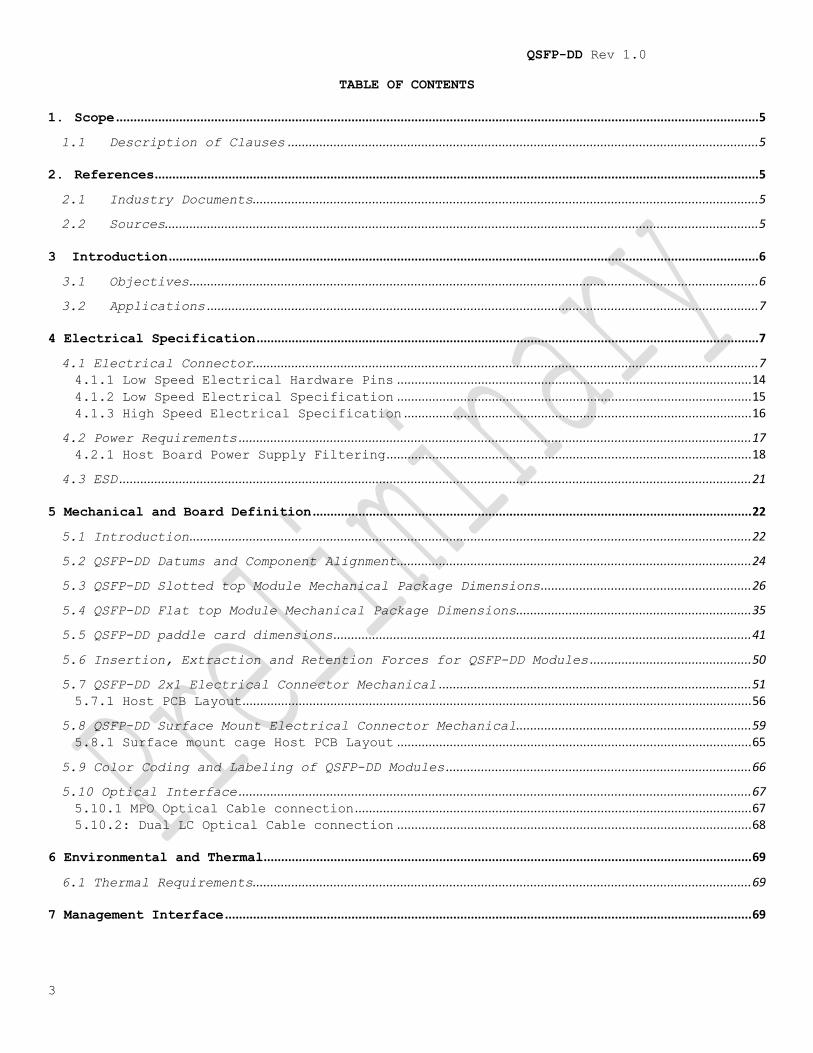
TABLE OF CONTENTS
1. Scope ....................................................................................................................................................................................... 5
1.1 Description of Clauses ...................................................................................................................................... 5
2. References ............................................................................................................................................................................ 5
2.1 Industry Documents................................................................................................................................................ 5
2.2 Sources......................................................................................................................................................................... 5
3 Introduction ........................................................................................................................................................................ 6
3.1 Objectives .................................................................................................................................................................. 6
3.2 Applications ............................................................................................................................................................. 7
4 Electrical Specification ............................................................................................................................................... 7
4.1 Electrical Connector................................................................................................................................................ 7 4.1.1 Low Speed Electrical Hardware Pins ..................................................................................................... 14 4.1.2 Low Speed Electrical Specification ..................................................................................................... 15 4.1.3 High Speed Electrical Specification ................................................................................................... 16
4.2 Power Requirements .................................................................................................................................................. 17 4.2.1 Host Board Power Supply Filtering ........................................................................................................ 18
4.3 ESD .................................................................................................................................................................................... 21
5 Mechanical and Board Definition ............................................................................................................................. 22
5.1 Introduction ................................................................................................................................................................ 22
5.2 QSFP-DD Datums and Component Alignment ..................................................................................................... 24
5.3 QSFP-DD Slotted top Module Mechanical Package Dimensions ............................................................ 26
5.4 QSFP-DD Flat top Module Mechanical Package Dimensions................................................................... 35
5.5 QSFP-DD paddle card dimensions ....................................................................................................................... 41
5.6 Insertion, Extraction and Retention Forces for QSFP-DD Modules .............................................. 50
5.7 QSFP-DD 2x1 Electrical Connector Mechanical ......................................................................................... 51 5.7.1 Host PCB Layout ................................................................................................................................................. 56
5.8 QSFP-DD Surface Mount Electrical Connector Mechanical................................................................... 59 5.8.1 Surface mount cage Host PCB Layout ..................................................................................................... 65
5.9 Color Coding and Labeling of QSFP-DD Modules ....................................................................................... 66
5.10 Optical Interface .................................................................................................................................................. 67 5.10.1 MPO Optical Cable connection ................................................................................................................. 67 5.10.2: Dual LC Optical Cable connection ..................................................................................................... 68
6 Environmental and Thermal........................................................................................................................................... 69
6.1 Thermal Requirements.............................................................................................................................................. 69
7 Management Interface ...................................................................................................................................................... 69
QSFP-DD Rev 1.0
4
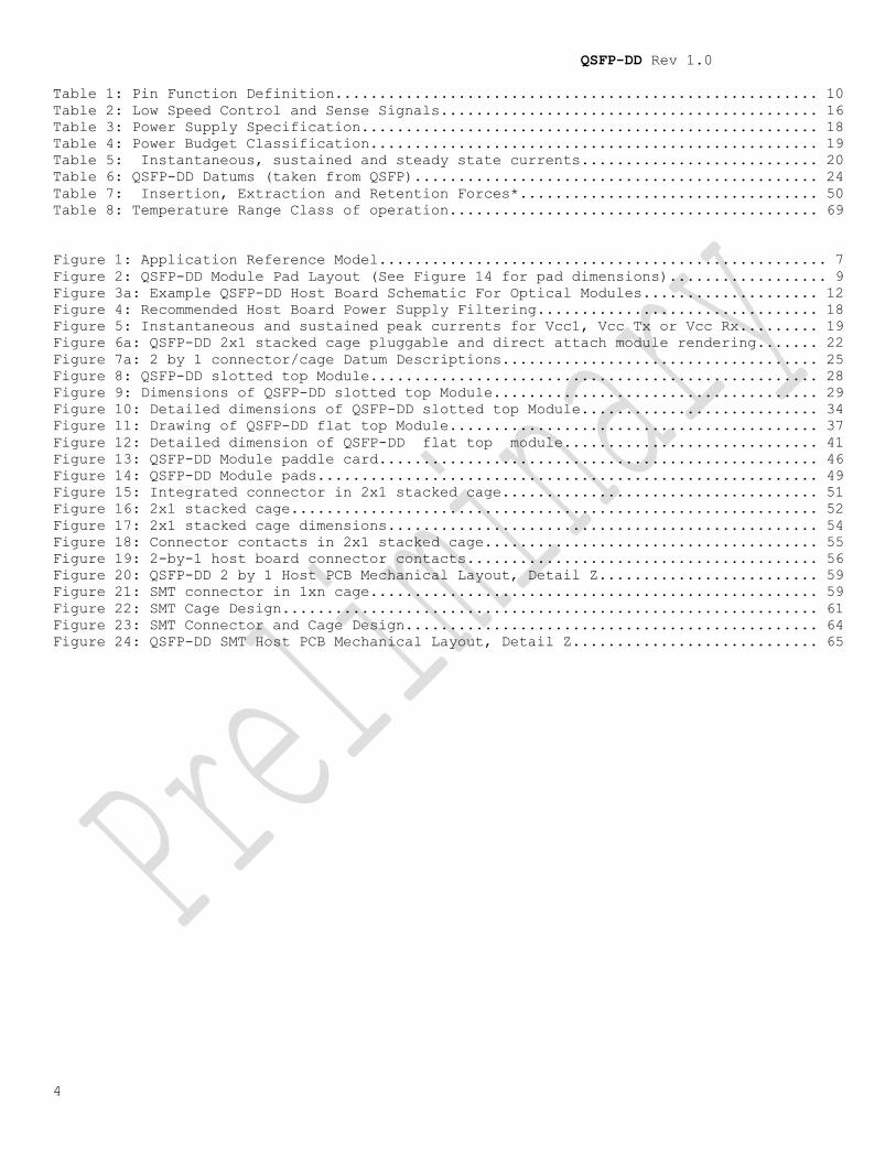
Table 1: Pin Function Definition....................................................... 10 Table 2: Low Speed Control and Sense Signals........................................... 16 Table 3: Power Supply Specification.................................................... 18 Table 4: Power Budget Classification................................................... 19 Table 5: Instantaneous, sustained and steady state currents........................... 20 Table 6: QSFP-DD Datums (taken from QSFP).............................................. 24 Table 7: Insertion, Extraction and Retention Forces*.................................. 50 Table 8: Temperature Range Class of operation.......................................... 69
Figure 1: Application Reference Model................................................... 7 Figure 2: QSFP-DD Module Pad Layout (See Figure 14 for pad dimensions).................. 9 Figure 3a: Example QSFP-DD Host Board Schematic For Optical Modules.................... 12 Figure 4: Recommended Host Board Power Supply Filtering................................ 18 Figure 5: Instantaneous and sustained peak currents for Vcc1, Vcc Tx or Vcc Rx......... 19 Figure 6a: QSFP-DD 2x1 stacked cage pluggable and direct attach module rendering....... 22 Figure 7a: 2 by 1 connector/cage Datum Descriptions.................................... 25 Figure 8: QSFP-DD slotted top Module................................................... 28 Figure 9: Dimensions of QSFP-DD slotted top Module..................................... 29 Figure 10: Detailed dimensions of QSFP-DD slotted top Module........................... 34 Figure 11: Drawing of QSFP-DD flat top Module.......................................... 37 Figure 12: Detailed dimension of QSFP-DD flat top module............................. 41 Figure 13: QSFP-DD Module paddle card.................................................. 46 Figure 14: QSFP-DD Module pads......................................................... 49 Figure 15: Integrated connector in 2x1 stacked cage.................................... 51 Figure 16: 2x1 stacked cage............................................................ 52 Figure 17: 2x1 stacked cage dimensions................................................. 54 Figure 18: Connector contacts in 2x1 stacked cage...................................... 55 Figure 19: 2-by-1 host board connector contacts........................................ 56 Figure 20: QSFP-DD 2 by 1 Host PCB Mechanical Layout, Detail Z......................... 59 Figure 21: SMT connector in 1xn cage................................................... 59 Figure 22: SMT Cage Design............................................................. 61 Figure 23: SMT Connector and Cage Design............................................... 64 Figure 24: QSFP-DD SMT Host PCB Mechanical Layout, Detail Z............................ 65
QSFP-DD Rev 1.0
5
QSFP-DD 8X Pluggable Transceiver
1. Scope
The scope of this specification is the definition of a high density 8-lane (8x) module,
cage and connector system. QSFP-DD supports up to 400 Gb/s in aggregate over an 8 x 50
Gb/s electrical interface. The cage and connector design provides backwards
compatibility to QSFP28 modules which can be inserted into 4 of the 8 electrical lanes.
1.1 Description of Clauses
Clause 1 Scope and Purpose
Clause 2 Referenced and Related Standards and SFF Specifications
Clause 3 introduction
Clause 4 electrical specifications
Clause 5 mechanical specifications and printed circuit board recommendations
Clause 6 environmental and thermal considerations
Clause 7 management interface, initialization and management register contents.
2. References
2.1 Industry Documents
The following interface standards and specifications are relevant to this Specification.
- GR-253-CORE
- IEEE Std 802.3
- IEEE Std 802.3by
- IEEE Std 802.3bs
- IEEE Std 802.3cd
- InfiniBand Architecture Specifications
- FC-PI-6p
- FC-PI-7
SFF Specifications
- INF-8436 QSFP (Quad SFP) 4 Gbps 4X Transceiver
- SFF-8636 Shielded Cables Common Management Interface
- SFF-8472 Diagnostic Monitoring Interface for Optical Transceivers
- SFF-8661 QSFP+ 4X Pluggable Module
- SFF-8679 QSFP28 4X Base Electrical Specification
2.2 Sources
This document can be obtained via the QSFP-DD.com web site.
QSFP-DD Rev 1.0
6
3 Introduction
This Specification covers the following items:
a) electrical interfaces including pad assignments for data, control, status and power
supplies and host PCB layout requirements.
b) management interface encompassing features from SFF-8636 with extensions for 8x
electrical lanes and 400Gb/s data path.
c) optical interfaces (including optical receptacles and mating fiber plugs for
multimode and single-mode duplex and parallel fiber applications). Breakout cable
applications are also specified. Optical signaling specifications are referenced from
the applicable standards.
d) mechanical specifications including dimensions and tolerances for the connector, cage
and module system. Includes details of the requirements for correct mating of the module
and host sides of the connector.
e) thermal requirements are based on data center applications
f) electromagnetic interference (EMI) recommendations(including necessary shielding
features to seal the OEM chassis front panel output with and without the QSFP-DD module
installed in the cage.
g) electrostatic discharge (ESD) requirements by reference to industry standard limits
and test methods.
Solely to the extent disclosed in the specification where the sole purpose of such
disclosure is to enable products to operate, connect or communicate as defined within the
specifications
3.1 Objectives
The overall package dimension shall conform to the indicated dimensions and tolerances
indicated in clause 5. The mounting features shall be located such that the products are
mechanically interchangeable with the cage and connector system. In addition, the overall
dimensions and mounting requirements for the cage and connector system on a circuit board
shall be configured such that the products are mechanically and electrically
interchangeable and the overall dimensions and insertion requirements for the optical
connector and corresponding fiber optic cable plug shall be such that the products are
mechanically and optically interchangeable.
The electrical and optical specifications may be compatible with those enumerated in the
ITU-T Recommendation G.957 , Telcordia Technologies GR-253-CORE, Ethernet IEEE 802.3
(10G/25G/40G/50G/100G/200G/400Gigabit), Infiniband Architecture Specifications and Fibre
Channel-PI-6/7 (32GFC and 64GFC). Electrical and optical specifications may be compatible
with standards under development.
QSFP-DD Rev 1.0
7
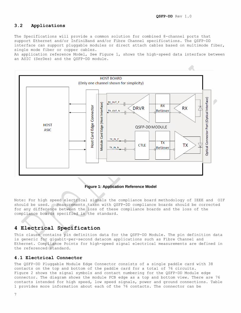
3.2 Applications
The Specifications will provide a common solution for combined 8-channel ports that
support Ethernet and/or InfiniBand and/or Fibre Channel specifications. The QSFP-DD
interface can support pluggable modules or direct attach cables based on multimode fiber,
single mode fiber or copper cables.
An application reference Model, See Figure 1, shows the high-speed data interface between
an ASIC (SerDes) and the QSFP-DD module.
Figure 1: Application Reference Model
Note: For high speed electrical signals the compliance board methodology of IEEE and OIF
should be used. Measurements taken with QSFP-DD compliance boards should be corrected
for any difference between the loss of these compliance boards and the loss of the
compliance boards specified in the standard.
4 Electrical Specification
This clause contains pin definition data for the QSFP-DD Module. The pin definition data
is generic for gigabit-per-second datacom applications such as Fibre Channel and
Ethernet. Compliance Points for high-speed signal electrical measurements are defined in
the referenced standard.
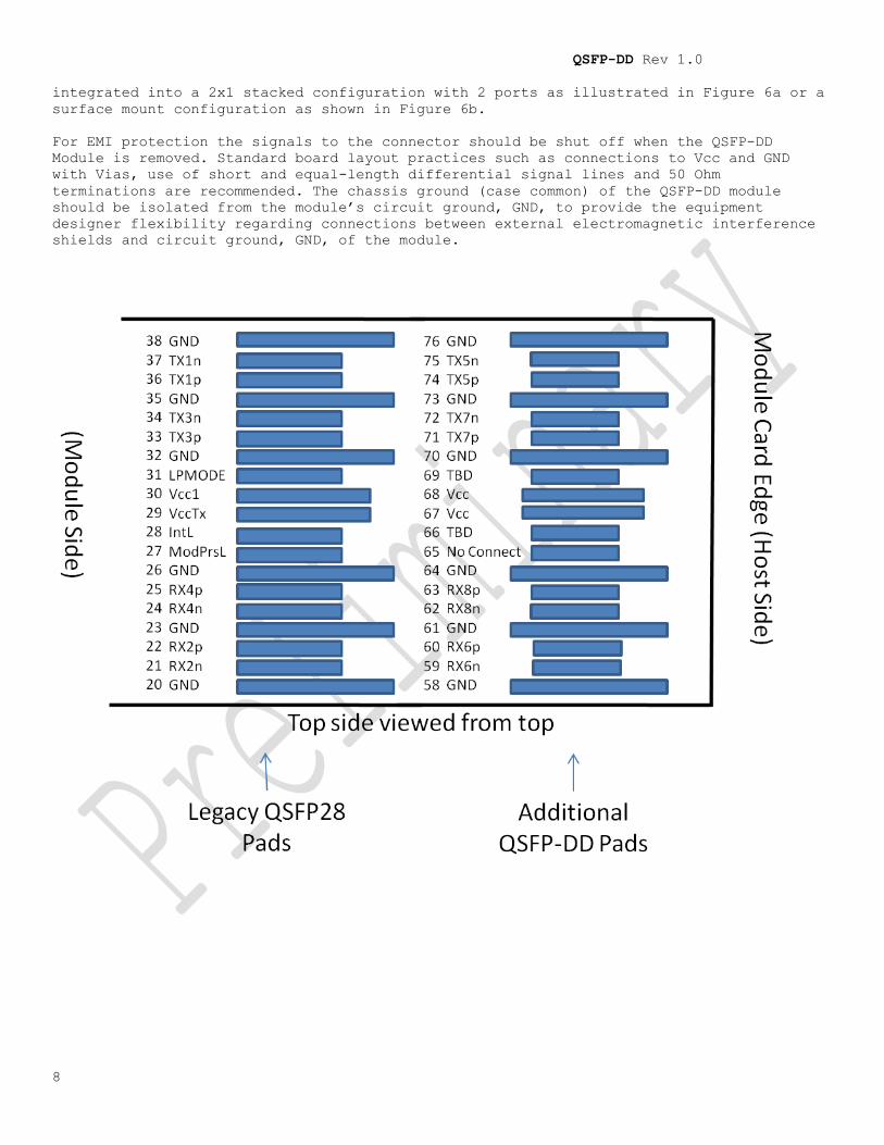
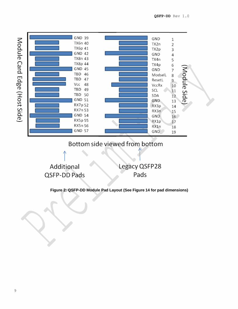
4.1 Electrical Connector
The QSFP-DD Pluggable Module Edge Connector consists of a single paddle card with 38
contacts on the top and bottom of the paddle card for a total of 76 circuits.
Figure 2 shows the signal symbols and contact numbering for the QSFP-DD Module edge
connector. The diagram shows the module PCB edge as a top and bottom view. There are 76
contacts intended for high speed, low speed signals, power and ground connections. Table
1 provides more information about each of the 76 contacts. The connector can be
QSFP-DD Rev 1.0
8
integrated into a 2x1 stacked configuration with 2 ports as illustrated in Figure 6a or a
surface mount configuration as shown in Figure 6b.
For EMI protection the signals to the connector should be shut off when the QSFP-DD
Module is removed. Standard board layout practices such as connections to Vcc and GND
with Vias, use of short and equal-length differential signal lines and 50 Ohm
terminations are recommended. The chassis ground (case common) of the QSFP-DD module
should be isolated from the module’s circuit ground, GND, to provide the equipment
designer flexibility regarding connections between external electromagnetic interference
shields and circuit ground, GND, of the module.
QSFP-DD Rev 1.0
9
Figure 2: QSFP-DD Module Pad Layout (See Figure 14 for pad dimensions)
QSFP-DD Rev 1.0
10
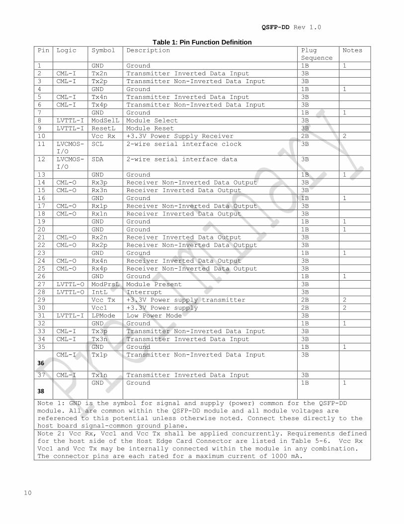
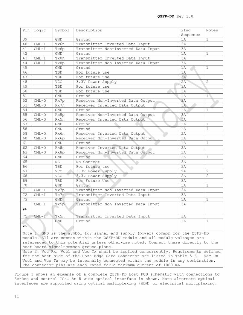
Table 1: Pin Function Definition Pin Logic Symbol Description Plug
Sequence
Notes
1 GND Ground 1B 1
2 CML-I Tx2n Transmitter Inverted Data Input 3B
3 CML-I Tx2p Transmitter Non-Inverted Data Input 3B
4 GND Ground 1B 1
5 CML-I Tx4n Transmitter Inverted Data Input 3B
6 CML-I Tx4p Transmitter Non-Inverted Data Input 3B
7 GND Ground 1B 1
8 LVTTL-I ModSelL Module Select 3B
9 LVTTL-I ResetL Module Reset 3B
10 Vcc Rx +3.3V Power Supply Receiver 2B 2
11 LVCMOS-
I/O
SCL 2-wire serial interface clock 3B
12 LVCMOS-
I/O
SDA 2-wire serial interface data 3B
13 GND Ground 1B 1
14 CML-O Rx3p Receiver Non-Inverted Data Output 3B
15 CML-O Rx3n Receiver Inverted Data Output 3B
16 GND Ground 1B 1
17 CML-O Rx1p Receiver Non-Inverted Data Output 3B
18 CML-O Rx1n Receiver Inverted Data Output 3B
19 GND Ground 1B 1
20 GND Ground 1B 1
21 CML-O Rx2n Receiver Inverted Data Output 3B
22 CML-O Rx2p Receiver Non-Inverted Data Output 3B
23 GND Ground 1B 1
24 CML-O Rx4n Receiver Inverted Data Output 3B
25 CML-O Rx4p Receiver Non-Inverted Data Output 3B
26 GND Ground 1B 1
27 LVTTL-O ModPrsL Module Present 3B
28 LVTTL-O IntL Interrupt 3B
29 Vcc Tx +3.3V Power supply transmitter 2B 2
30 Vcc1 +3.3V Power supply 2B 2
31 LVTTL-I LPMode Low Power Mode 3B
32 GND Ground 1B 1
33 CML-I Tx3p Transmitter Non-Inverted Data Input 3B
34 CML-I Tx3n Transmitter Inverted Data Input 3B
35 GND Ground 1B 1
36
CML-I Tx1p Transmitter Non-Inverted Data Input 3B
37 CML-I Tx1n Transmitter Inverted Data Input 3B
38
GND Ground 1B 1
Note 1: GND is the symbol for signal and supply (power) common for the QSFP-DD
module. All are common within the QSFP-DD module and all module voltages are
referenced to this potential unless otherwise noted. Connect these directly to the
host board signal-common ground plane.
Note 2: Vcc Rx, Vcc1 and Vcc Tx shall be applied concurrently. Requirements defined
for the host side of the Host Edge Card Connector are listed in Table 5-6. Vcc Rx
Vcc1 and Vcc Tx may be internally connected within the module in any combination.
The connector pins are each rated for a maximum current of 1000 mA.
QSFP-DD Rev 1.0
11
Pin Logic Symbol Description Plug
Sequence
Notes
39 GND Ground 1A 1
40 CML-I Tx6n Transmitter Inverted Data Input 3A
41 CML-I Tx6p Transmitter Non-Inverted Data Input 3A
42 GND Ground 1A 1
43 CML-I Tx8n Transmitter Inverted Data Input 3A
44 CML-I Tx8p Transmitter Non-Inverted Data Input 3A
45 GND Ground 1A 1
46 TBD For future use 3A
47 TBD For future use 3A
48 VCC 3.3V Power Supply 2A 2
49 TBD For future use 3A
50 TBD For future use 3A
51 GND Ground 1A 1
52 CML-O Rx7p Receiver Non-Inverted Data Output 3A
53 CML-O Rx7n Receiver Inverted Data Output 3A
54 GND Ground 1A 1
55 CML-O Rx5p Receiver Non-Inverted Data Output 3A
56 CML-O Rx5n Receiver Inverted Data Output 3A
57 GND Ground 1A 1
58 GND Ground 1A 1
59 CML-O Rx6n Receiver Inverted Data Output 3A
60 CML-O Rx6p Receiver Non-Inverted Data Output 3A
61 GND Ground 1A 1
62 CML-O Rx8n Receiver Inverted Data Output 3A
63 CML-O Rx8p Receiver Non-Inverted Data Output 3A
64 GND Ground 1A 1
65 NC No Connect 3A
66 TBD For future use 3A
67 VCC 3.3V Power Supply 2A 2
68 VCC 3.3V Power Supply 2A 2
69 TBD For Future Use 3A
70 GND Ground 1A 1
71 CML-I Tx7p Transmitter Non-Inverted Data Input 3A
72 CML-I Tx7n Transmitter Inverted Data Input 3A
73 GND Ground 1A 1
74
CML-I Tx5p Transmitter Non-Inverted Data Input 3A
75 CML-I Tx5n Transmitter Inverted Data Input 3A
76
GND Ground 1A 1
Note 1: GND is the symbol for signal and supply (power) common for the QSFP-DD
module. All are common within the QSFP-DD module and all module voltages are
referenced to this potential unless otherwise noted. Connect these directly to the
host board signal-common ground plane.
Note 2: Vcc Rx, Vcc1 and Vcc Tx shall be applied concurrently. Requirements defined
for the host side of the Host Edge Card Connector are listed in Table 5-6. Vcc Rx
Vcc1 and Vcc Tx may be internally connected within the module in any combination.
The connector pins are each rated for a maximum current of 1000 mA.
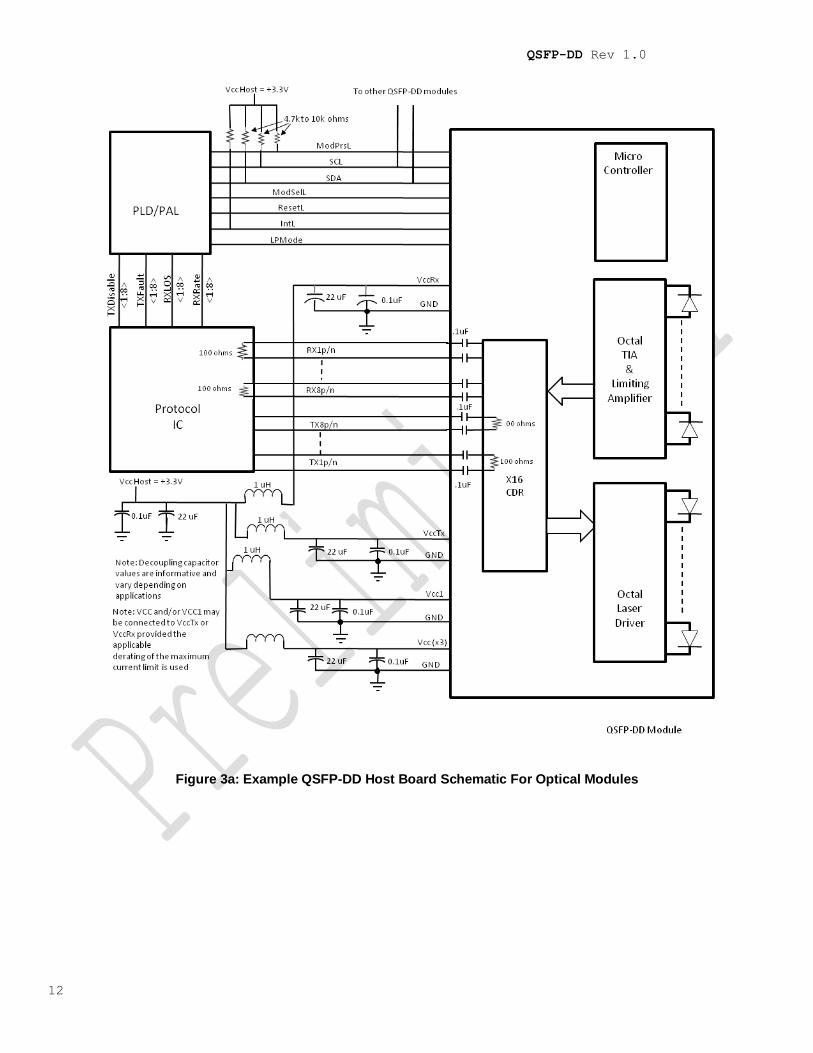
Figure 3 shows an example of a complete QSFP-DD host PCB schematic with connections to
SerDes and control ICs. An 8 wide optical interface is shown. Note alternate optical
interfaces are supported using optical multiplexing (WDM) or electrical multiplexing.
QSFP-DD Rev 1.0
12
Figure 3a: Example QSFP-DD Host Board Schematic For Optical Modules
QSFP-DD Rev 1.0
13
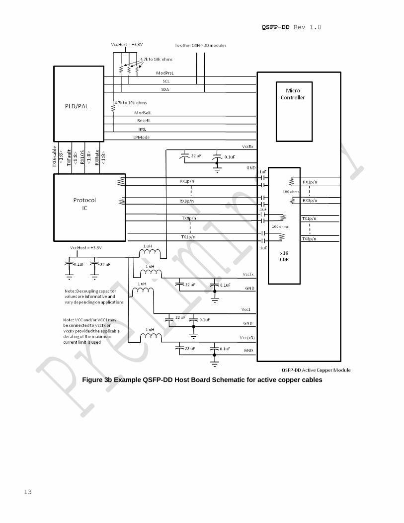
Figure 3b Example QSFP-DD Host Board Schematic for active copper cables
QSFP-DD Rev 1.0
14
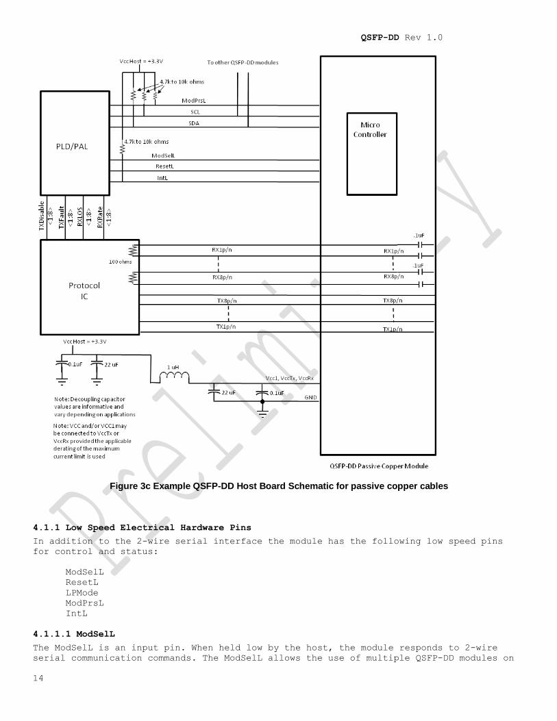
Figure 3c Example QSFP-DD Host Board Schematic for passive copper cables
4.1.1 Low Speed Electrical Hardware Pins
In addition to the 2-wire serial interface the module has the following low speed pins
for control and status:
ModSelL
ResetL
LPMode
ModPrsL
IntL
4.1.1.1 ModSelL
The ModSelL is an input pin. When held low by the host, the module responds to 2-wire
serial communication commands. The ModSelL allows the use of multiple QSFP-DD modules on

QSFP-DD Rev 1.0
15
a single 2-wire interface bus. When the ModSelL is “High”, the module shall not respond
to or acknowledge any 2-wire interface communication from the host. ModSelL signal input
node must be biased to the “High” state in the module.
In order to avoid conflicts, the host system shall not attempt 2-wire interface
communications within the ModSelL de-assert time after any QSFP-DD modules are
deselected. Similarly, the host must wait at least for the period of the ModSelL assert
time before communicating with the newly selected module. The assertion and de-asserting
periods of different modules may overlap as long as the above timing requirements are
met.
4.1.1.2 ResetL
The ResetL pin must be pulled to Vcc in the QSFP-DD module. A low level on the ResetL pin
for longer than the minimum pulse length (t_Reset_init) initiates a complete module
reset, returning all user module settings to their default state. Module Reset Assert
Time (t_init) starts on the rising edge after the low level on the ResetL pin is
released. During the execution of a reset (t_init) the host shall disregard all status
bits until the module indicates a completion of the reset interrupt. The module indicates
this by asserting “low” an IntL signal with the Data_Not_Ready bit negated. Note that on
power up (including hot insertion) the module should post this completion of reset
interrupt without requiring a reset.
4.1.1.3 LPMode
The LPMode pin shall be pulled up to Vcc in the QSFP-DD module. The transition from Low
Power mode to High Power mode and the power classes are all defined in Section 4.2.
4.1.1.4 ModPrsL
ModPrsL is pulled up to Vcc_Host on the host board and grounded in the module. The
ModPrsL is asserted “Low” when inserted and deasserted “High” when the module is
physically absent from the host connector.
4.1.1.5 IntL
IntL is an output pin. When “Low”, it indicates a possible module operational fault or a
status critical to the host system. The host identifies the source of the interrupt using
the 2-wire serial interface. The IntL pin is an open collector output and must be pulled
to host supply voltage on the host board. The INTL pin is deasserted “High” after
completion of reset, when byte 2 bit 0 (Data Not Ready)is read with a value of ‘0’ and
the flag field is read (see 7.6.1.2).
4.1.2 Low Speed Electrical Specification
Low speed signaling other than SCL and SDA is based on Low Voltage TTL (LVTTL) operating
at Vcc. Vcc refers to the generic supply voltages of VccTx, VccRx, Vcc_host or Vcc1.
Hosts shall use a pull-up resistor connected to Vcc_host on each of the 2-wire interface
SCL (clock), SDA (data), and all low speed status outputs. The SCL and SDA is a hot plug
interface that may support a bus topology. During module insertion or removal, the module
may implement a pre-charge circuit which prevents corrupting data transfers from other
modules that are already using the bus.
Note 1-Timing diagrams for SCL and SDA are included in Subclause 7.2.2.
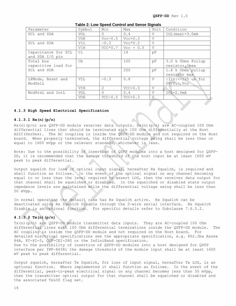
The QSFP-DD low speed electrical specifications are given in Table 2. This specification
ensures compatibility between host bus masters and the 2-wire interface.
QSFP-DD Rev 1.0
16
Table 2: Low Speed Control and Sense Signals Parameter Symbol Min Max Unit Condition
SCL and SDA VOL 0 0.4 V IOL(max)=3.0mA
VOH Vcc-0.5 Vcc+0.3 V
SCL and SDA VIL -0.3 Vcc*0.3 V
VIH VCC*0.7 Vcc + 0.5 V
Capacitance for SCL
and SDA I/O pin
Ci 14 pF
Total bus
capacitive load for
SCL and SDA
Cb 100 pF 3.0 k Ohms Pullup
resistor, max
200 pF 1.6 k Ohms pullup
resistor max
LPMode, Reset and
ModSelL
VIL -0.3 0.8 V |Iin|<=125 uA for
0V<Vin,Vcc
VIH 2 VCC+0.3 V
ModPrsL and IntL VOL 0 0.4 V IOL=2.0mA
VOH VCC-0.5 VCC+0.3 V
4.1.3 High Speed Electrical Specification
4.1.3.1 Rx(n)(p/n)
Rx(n)(p/n) are QSFP-DD module receiver data outputs. Rx(n)(p/n) are AC-coupled 100 Ohm
differential lines that should be terminated with 100 Ohm differentially at the Host
ASIC(SerDes). The AC coupling is inside the QSFP-DD module and not required on the Host
board. When properly terminated, the differential voltage swing shall be less than or
equal to 1600 mVpp or the relevant standard, whichever is less.
Note: Due to the possibility of insertion of QSFP modules into a host designed for QSFP-
DD, it is recommended that the damage threshold of the host input be at least 1600 mV
peak to peak differential.
Output squelch for loss of optical input signal, hereafter Rx Squelch, is required and
shall function as follows. In the event of the optical signal on any channel becoming
equal to or less than the level required to assert LOS, then the receiver data output for
that channel shall be squelched or disabled. In the squelched or disabled state output
impedance levels are maintained while the differential voltage swing shall be less than
50 mVpp.
In normal operation the default case has Rx Squelch active. Rx Squelch can be
deactivated using Rx Squelch Disable through the 2-wire serial interface. Rx Squelch
Disable is an optional function. For specific details refer to Subclause 7.6.5.2.
4.1.3.2 Tx(n)(p/n)
Tx(n)(p/n) are QSFP-DD module transmitter data inputs. They are AC-coupled 100 Ohm
differential lines with 100 Ohm differential terminations inside the QSFP-DD module. The
AC coupling is inside the QSFP-DD module and not required on the Host board. For
detailed electrical specifications see the appropriate specification, e.g. 802.3ba Annex
86A, FC-PI-5, OIF-CEI-28G or the InfiniBand specification.
Due to the possibility of insertion of QSFP-DD modules into a host designed for QSFP
interface per INF-8438i the damage threshold of the module input shall be at least 1600
mV peak to peak differential.
Output squelch, hereafter Tx Squelch, for loss of input signal, hereafter Tx LOS, is an
optional function. Where implemented it shall function as follows. In the event of the
differential, peak-to-peak electrical signal on any channel becomes less than 50 mVpp,
then the transmitter optical output for that channel shall be squelched or disabled and
the associated TxLOS flag set.
QSFP-DD Rev 1.0
17
Where squelched, the transmitter OMA shall be less than or equal to -26 dBm and when
disabled the transmitter power shall be less than or equal to -30 dBm. For applications,
e.g. Ethernet, where the transmitter off condition is defined in terms of average power,
disabling the transmitter is recommended and for applications, e.g. InfiniBand, where the
transmitter off condition is defined in terms of OMA, squelching the transmitter is
recommended.
In module operation, where Tx Squelch is implemented, the default case has Tx Squelch
active. Tx Squelch can be deactivated using Tx Squelch Disable through the 2-wire serial
interface. Tx Squelch Disable is an optional function. For specific details refer to
Clause 7.6.5.2.
4.2 Power Requirements
The power supply has six designated pins, VccTx, Vcc1, VccRx and 3 additional Vcc pins in
the connector. Vcc1 and Vcc are used to supplement VccTx or VccRx at the discretion of
the module vendor. Power is applied concurrently to these pins.
Since different classes of modules exist with pre-defined maximum power consumption
limits, it is necessary to avoid exceeding the system power supply limits and cooling
capacity when a module is inserted into a system designed to only accommodate lower power
modules. It is recommended that the host, through the management interface, identify the
power consumption class of the module before allowing the module to go into high power
mode.
A host board together with the QSFP-DD module(s) forms an integrated power system. The
host supplies stable power to the module. The module limits electrical noise coupled back
into the host system and limits inrush charge/current during hot plug insertion.
All specifications shall be met at the maximum power supply current. No power sequencing
of the power supply is required of the host system since the module sequences the
contacts in the order of ground, supply and signals during insertion.
QSFP-DD Rev 1.0
18
4.2.1 Host Board Power Supply Filtering
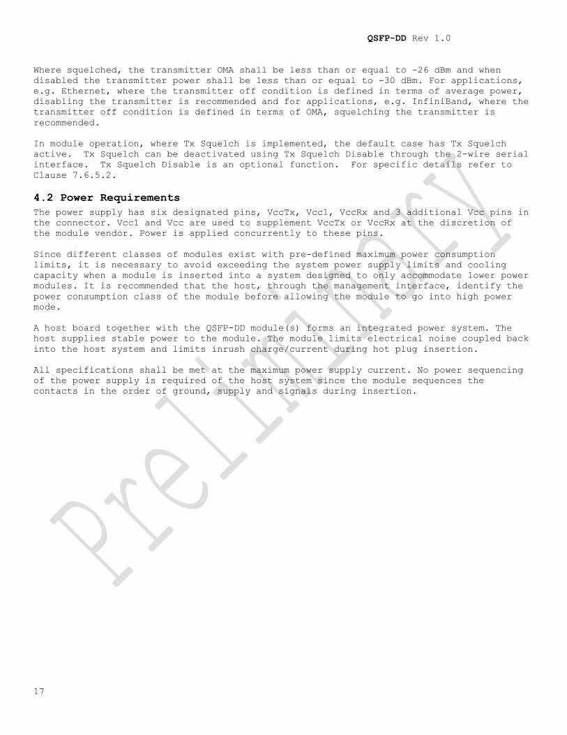
The host board should use the power supply filtering equivalent to that shown in Figure
4.
Figure 4: Recommended Host Board Power Supply Filtering
Any voltage drop across a filter network on the host is counted against the host DC set
point accuracy specification. Inductors with DC Resistance of less than 0.1 Ohm should be
used in order to maintain the required voltage at the Host Edge Card Connector. It is
recommended that the 22 uF capacitors each have an equivalent series resistance of 0.22
ohm.
The specification for the power supply is shown in Table 3.
Table 3: Power Supply Specification Parameter MIN Nominal Max Unit Condition
Vcc 3.3 V
Measured at Vcc Tx, Vcc Rx and Vcc1.
Vcc set point accuracy -5 5 % Measured at Vcc Tx, Vcc Rx and
Vcc1.
Power Supply Noise
including ripple
50 mV 1kHz to frequency of operation
measured at Vcc host.
Sustained peak current
at hot plug with LPMode
Pin asserted
495 mA See Figure 5
Maximum instantaneous
current with LPMode
asserted
600 mA See Figure 5
Module sustained peak
current with LPMode Pin
deasserted
TBD mA
Maximum instantaneous
current with LPMode
deasserted
TBD mA
These limits separately apply to the current that flows through each inductor in the
power supply filter.
QSFP-DD Rev 1.0
19
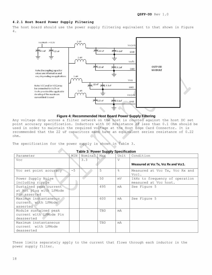
Figure 5: Instantaneous and sustained peak currents for Vcc1, Vcc Tx or Vcc Rx
Power levels associated with classifications of modules are shown in Table 4.
Table 4: Power Budget Classification Power Level Max Power (W)
1 1.5
2 2.5
3 3.5
4 4.5
5 5.5
6 6.5
7 7.5
8 8.5
9 >8.5
In general, the higher power classification level is associated with higher data rates
and longer reach. The system designer is responsible for ensuring that the maximum
temperature does not exceed the case temperature requirements.
QSFP-DD Rev 1.0
20
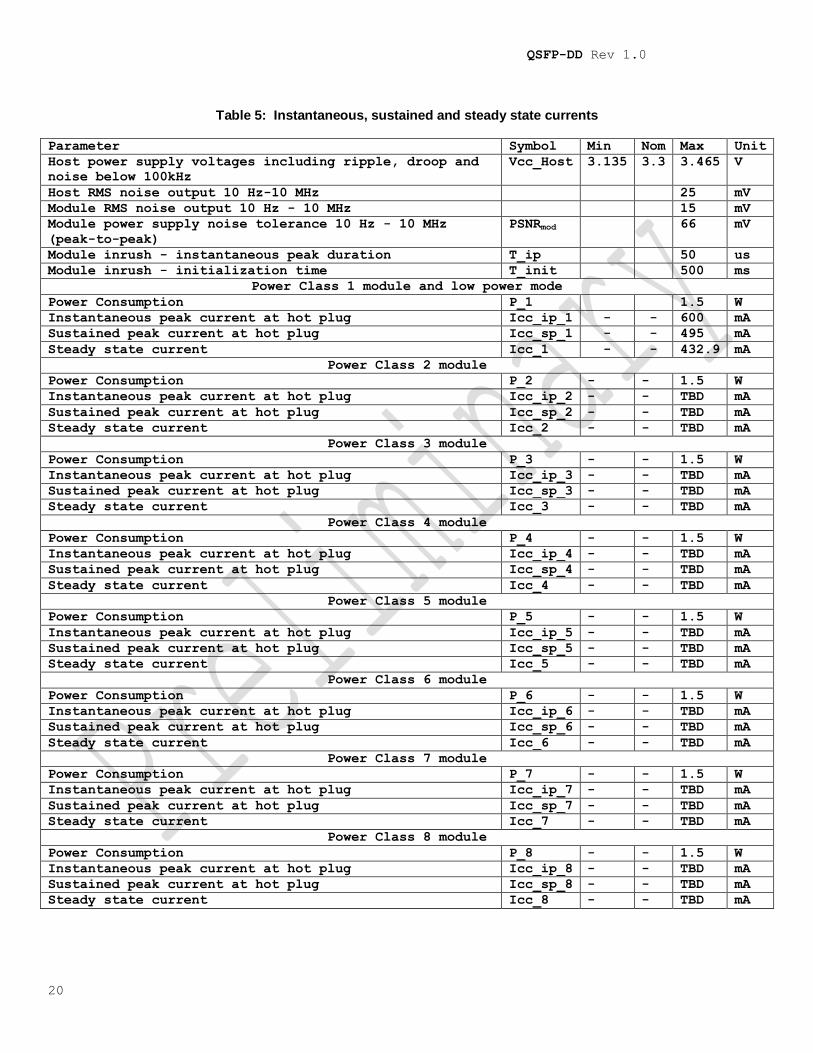
Table 5: Instantaneous, sustained and steady state currents
Parameter Symbol Min Nom Max Unit
Host power supply voltages including ripple, droop and
noise below 100kHz
Vcc_Host 3.135 3.3 3.465 V
Host RMS noise output 10 Hz-10 MHz 25 mV
Module RMS noise output 10 Hz - 10 MHz 15 mV
Module power supply noise tolerance 10 Hz - 10 MHz
(peak-to-peak)
PSNRmod 66 mV
Module inrush - instantaneous peak duration T_ip 50 us
Module inrush - initialization time T_init 500 ms
Power Class 1 module and low power mode
Power Consumption P_1 1.5 W
Instantaneous peak current at hot plug Icc_ip_1 - - 600 mA
Sustained peak current at hot plug Icc_sp_1 - - 495 mA
Steady state current Icc_1 - - 432.9 mA
Power Class 2 module
Power Consumption P_2 - - 1.5 W
Instantaneous peak current at hot plug Icc_ip_2 - - TBD mA
Sustained peak current at hot plug Icc_sp_2 - - TBD mA
Steady state current Icc_2 - - TBD mA
Power Class 3 module
Power Consumption P_3 - - 1.5 W
Instantaneous peak current at hot plug Icc_ip_3 - - TBD mA
Sustained peak current at hot plug Icc_sp_3 - - TBD mA
Steady state current Icc_3 - - TBD mA
Power Class 4 module
Power Consumption P_4 - - 1.5 W
Instantaneous peak current at hot plug Icc_ip_4 - - TBD mA
Sustained peak current at hot plug Icc_sp_4 - - TBD mA
Steady state current Icc_4 - - TBD mA
Power Class 5 module
Power Consumption P_5 - - 1.5 W
Instantaneous peak current at hot plug Icc_ip_5 - - TBD mA
Sustained peak current at hot plug Icc_sp_5 - - TBD mA
Steady state current Icc_5 - - TBD mA
Power Class 6 module
Power Consumption P_6 - - 1.5 W
Instantaneous peak current at hot plug Icc_ip_6 - - TBD mA
Sustained peak current at hot plug Icc_sp_6 - - TBD mA
Steady state current Icc_6 - - TBD mA
Power Class 7 module
Power Consumption P_7 - - 1.5 W
Instantaneous peak current at hot plug Icc_ip_7 - - TBD mA
Sustained peak current at hot plug Icc_sp_7 - - TBD mA
Steady state current Icc_7 - - TBD mA
Power Class 8 module
Power Consumption P_8 - - 1.5 W
Instantaneous peak current at hot plug Icc_ip_8 - - TBD mA
Sustained peak current at hot plug Icc_sp_8 - - TBD mA
Steady state current Icc_8 - - TBD mA

QSFP-DD Rev 1.0
21
4.3 ESD
Where ESD performance is not otherwise specified, e.g. in the InfiniBand specification,
the QSFP-DD module shall meet ESD requirements given in EN61000-4-2, criterion B test
specification when installed in a properly grounded cage and chassis. The units are
subjected to 15kV air discharges during operation and 8kV direct contact discharges to
the case. The QSFP-DD module and host high speed signal contacts shall withstand 1000 V
electrostatic discharge based on Human Body Model per JEDEC JESD22-A114-B.
The QSFP-DD module and all host contacts with exception of the module and host high speed
signal contacts shall withstand 2 kV electrostatic discharge based on Human Body Model
per JEDEC JESD22-A114-B.

QSFP-DD Rev 1.0
22
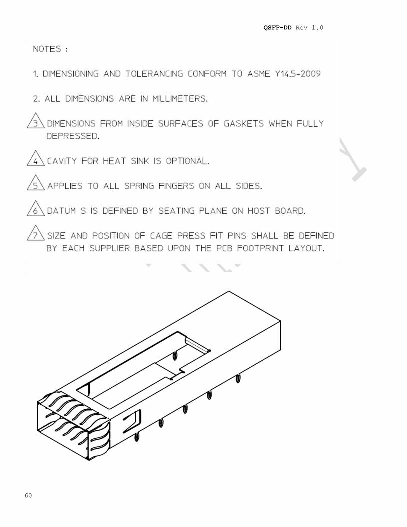
5 Mechanical and Board Definition
5.1 Introduction
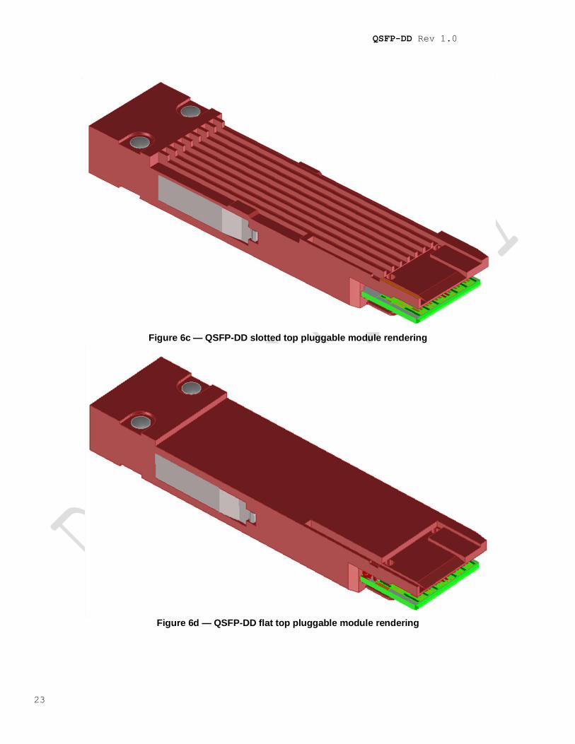
The modules and cages defined in this clause are illustrated in Figure 6. Figure 6a shows
the 2x1 stacked cage. Figure 6b shows the surface mount cage. Figure 6c shows the slotted
top pluggable module. Figure 6d shows the flat top module. All Pluggable modules and
direct attach cable plugs must mate to the connectors and cages defined in this
specification. Heat sink/clip thermal designs are application specific and not
specifically defined by this specification. Note: It is the intention of this MSA to
select a single module type from Figures 6c and 6d.
Figure 6a: QSFP-DD 2x1 stacked cage pluggable and direct attach module rendering
Figure 6b — QSFP-DD press fit cage for surface mount (SMT) connector
QSFP-DD Rev 1.0
23
Figure 6c — QSFP-DD slotted top pluggable module rendering
Figure 6d — QSFP-DD flat top pluggable module rendering
QSFP-DD Rev 1.0
24
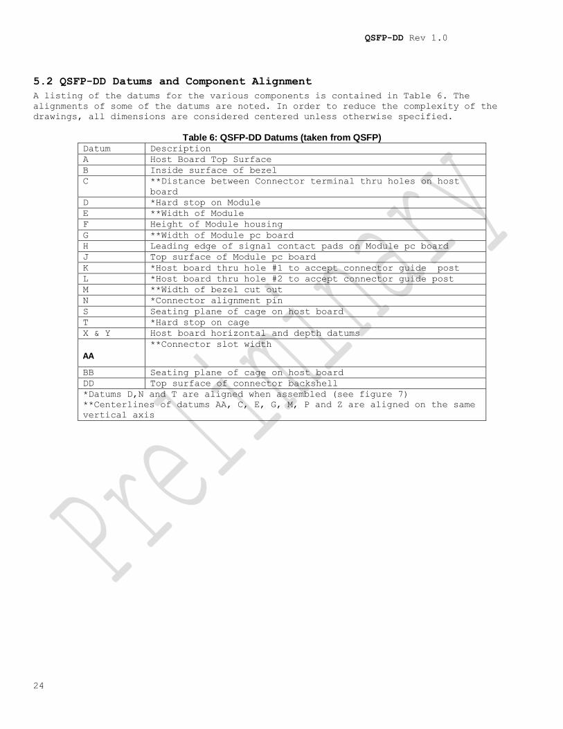
5.2 QSFP-DD Datums and Component Alignment
A listing of the datums for the various components is contained in Table 6. The
alignments of some of the datums are noted. In order to reduce the complexity of the
drawings, all dimensions are considered centered unless otherwise specified.
Table 6: QSFP-DD Datums (taken from QSFP) Datum Description
A Host Board Top Surface
B Inside surface of bezel
C **Distance between Connector terminal thru holes on host
board
D *Hard stop on Module
E **Width of Module
F Height of Module housing
G **Width of Module pc board
H Leading edge of signal contact pads on Module pc board
J Top surface of Module pc board
K *Host board thru hole #1 to accept connector guide post
L *Host board thru hole #2 to accept connector guide post
M **Width of bezel cut out
N *Connector alignment pin
S Seating plane of cage on host board
T *Hard stop on cage
X & Y Host board horizontal and depth datums
AA
**Connector slot width
BB Seating plane of cage on host board
DD Top surface of connector backshell
*Datums D,N and T are aligned when assembled (see figure 7)
**Centerlines of datums AA, C, E, G, M, P and Z are aligned on the same
vertical axis
QSFP-DD Rev 1.0
25
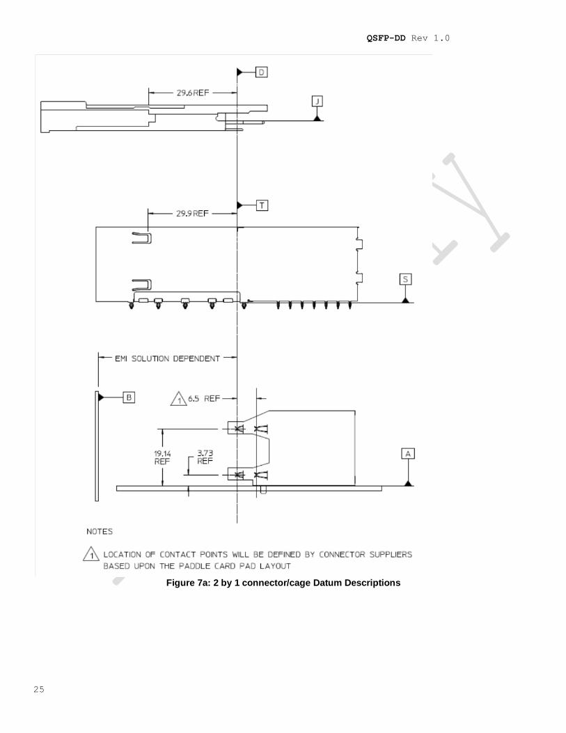
Figure 7a: 2 by 1 connector/cage Datum Descriptions
QSFP-DD Rev 1.0
26
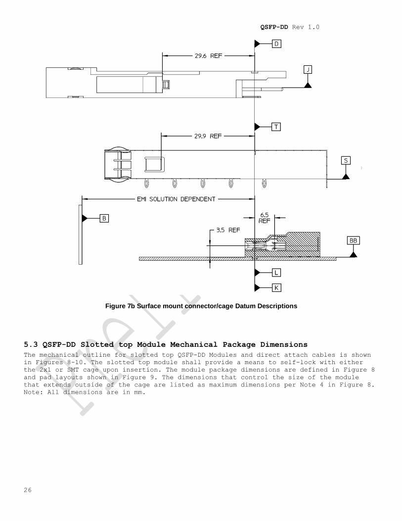
Figure 7b Surface mount connector/cage Datum Descriptions
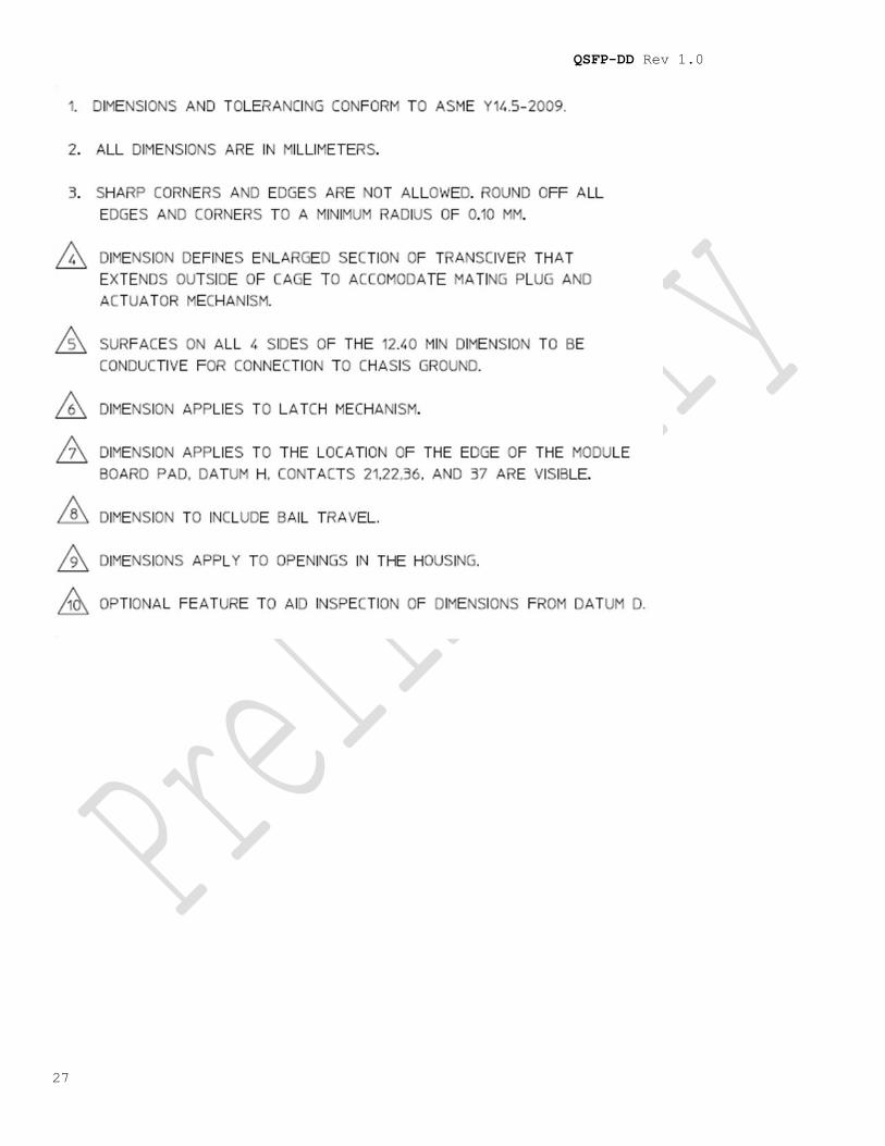
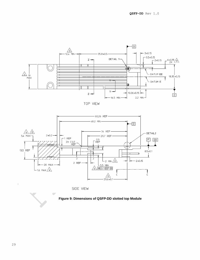
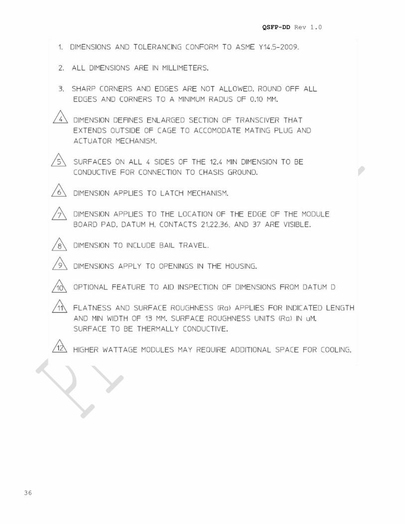
5.3 QSFP-DD Slotted top Module Mechanical Package Dimensions
The mechanical outline for slotted top QSFP-DD Modules and direct attach cables is shown
in Figures 8-10. The slotted top module shall provide a means to self-lock with either
the 2x1 or SMT cage upon insertion. The module package dimensions are defined in Figure 8
and pad layouts shown in Figure 9. The dimensions that control the size of the module
that extends outside of the cage are listed as maximum dimensions per Note 4 in Figure 8.
Note: All dimensions are in mm.
QSFP-DD Rev 1.0
27
QSFP-DD Rev 1.0
28
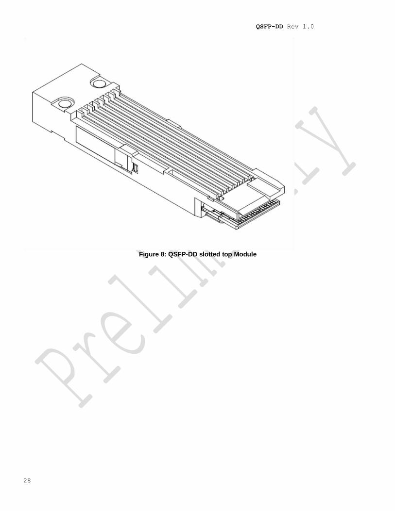
Figure 8: QSFP-DD slotted top Module
QSFP-DD Rev 1.0
29
Figure 9: Dimensions of QSFP-DD slotted top Module

QSFP-DD Rev 1.0
30
QSFP-DD Rev 1.0
31
QSFP-DD Rev 1.0
32
QSFP-DD Rev 1.0
33
QSFP-DD Rev 1.0
34
Figure 10: Detailed dimensions of QSFP-DD slotted top Module
QSFP-DD Rev 1.0
35
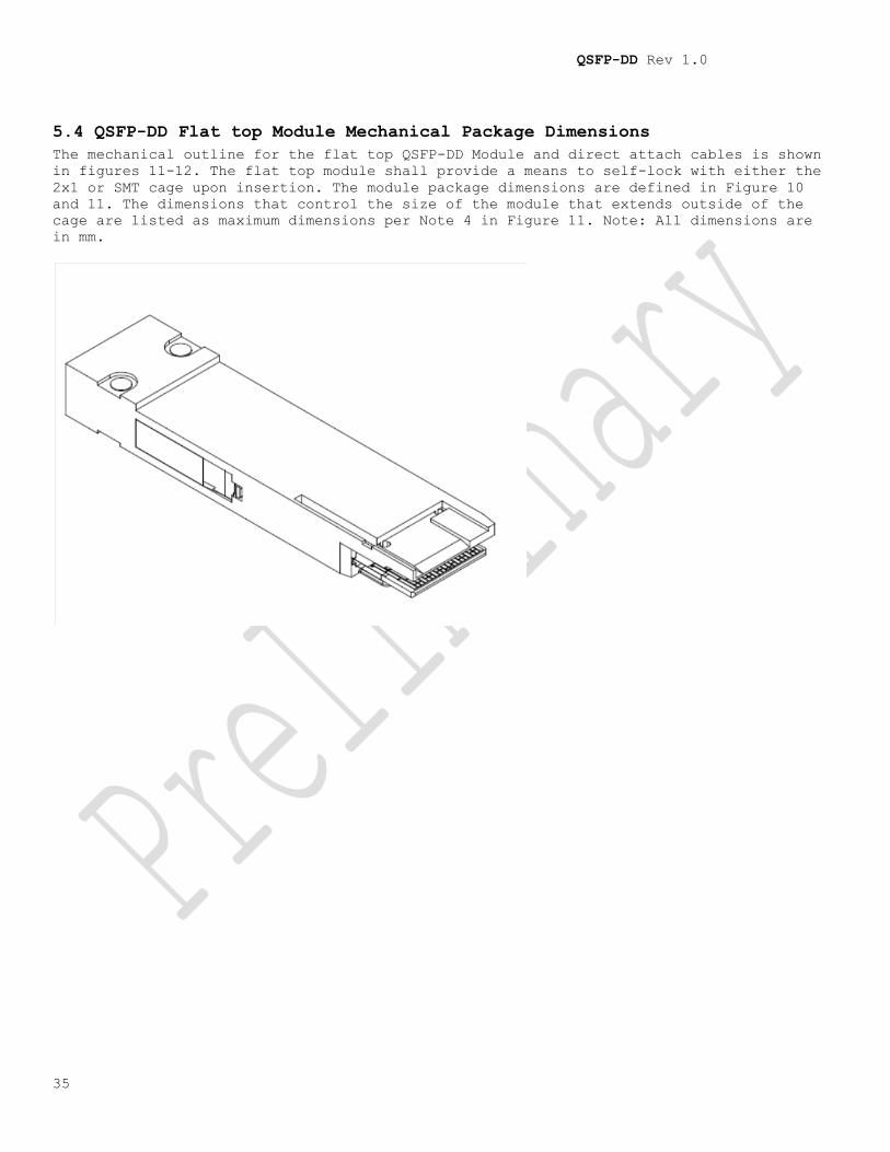
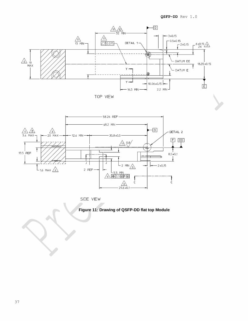
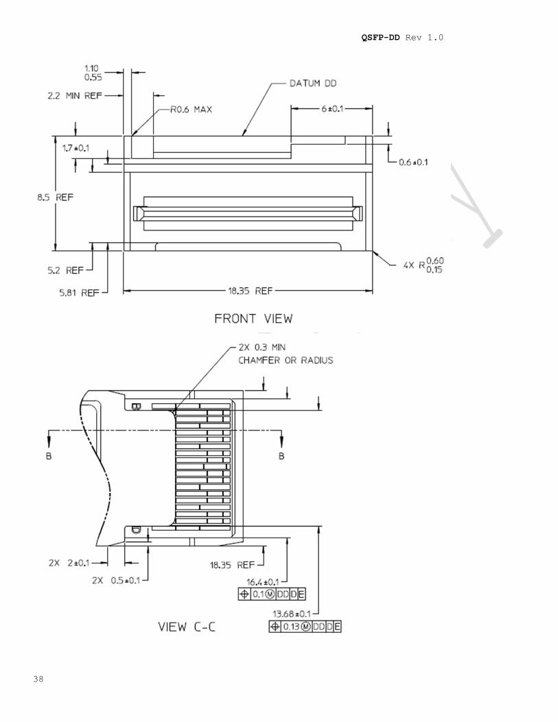
5.4 QSFP-DD Flat top Module Mechanical Package Dimensions
The mechanical outline for the flat top QSFP-DD Module and direct attach cables is shown
in figures 11-12. The flat top module shall provide a means to self-lock with either the
2x1 or SMT cage upon insertion. The module package dimensions are defined in Figure 10
and 11. The dimensions that control the size of the module that extends outside of the
cage are listed as maximum dimensions per Note 4 in Figure 11. Note: All dimensions are
in mm.
QSFP-DD Rev 1.0
36
QSFP-DD Rev 1.0
37
Figure 11: Drawing of QSFP-DD flat top Module
QSFP-DD Rev 1.0
38

QSFP-DD Rev 1.0
39
QSFP-DD Rev 1.0
40
QSFP-DD Rev 1.0
41
Figure 12: Detailed dimension of QSFP-DD flat top module
5.5 QSFP-DD paddle card dimensions
Note: The dimensions shown in this section apply to both slotted top and flat top modules
QSFP-DD Rev 1.0
42
QSFP-DD Rev 1.0
43
QSFP-DD Rev 1.0
44
QSFP-DD Rev 1.0
45
QSFP-DD Rev 1.0
46
Figure 13: QSFP-DD Module paddle card
QSFP-DD Rev 1.0
47
QSFP-DD Rev 1.0
48
QSFP-DD Rev 1.0
49
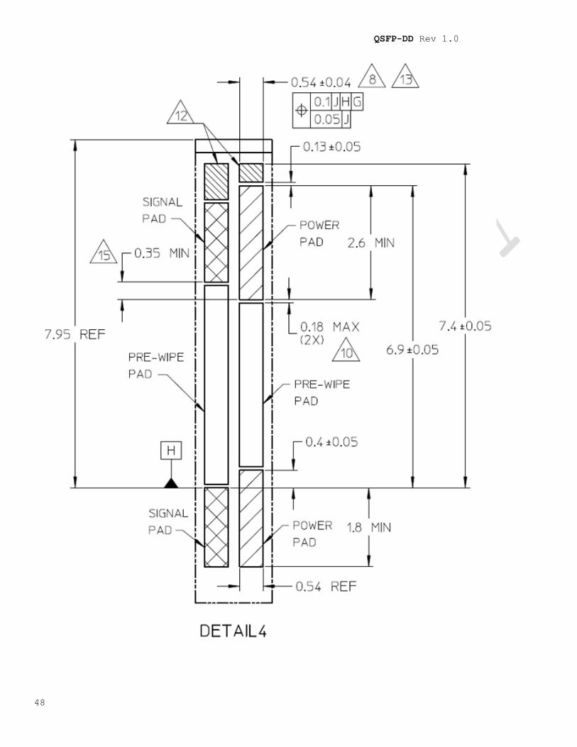
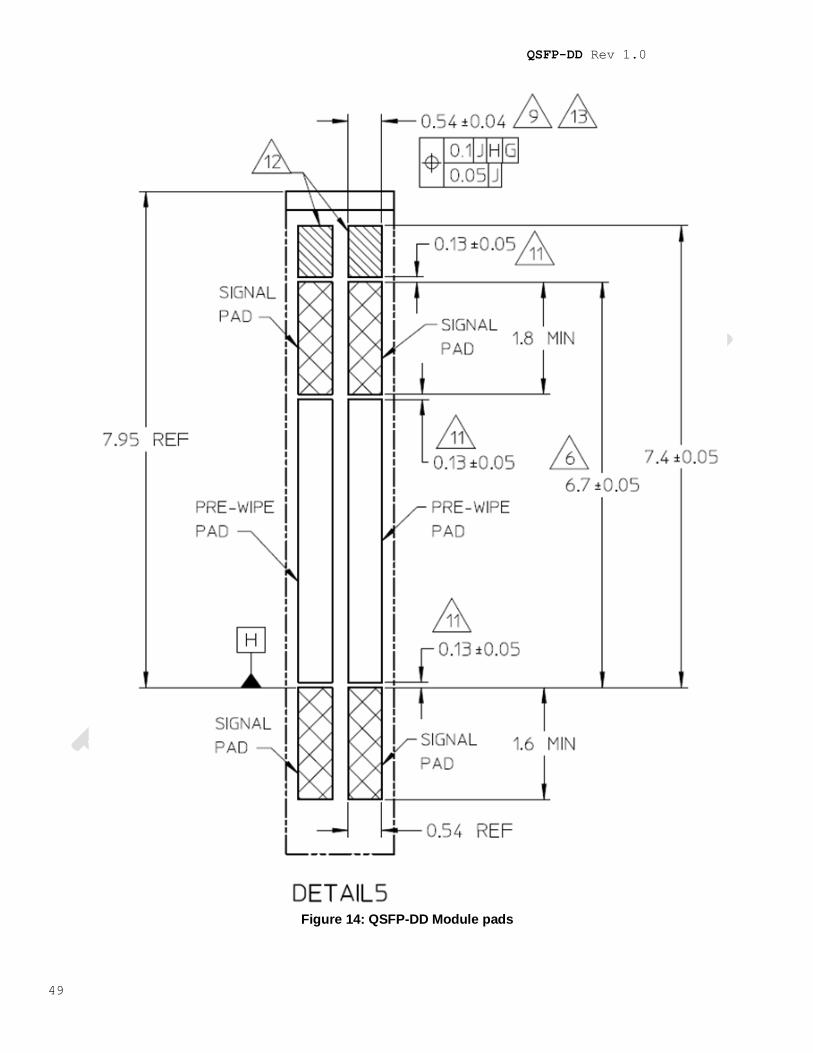
Figure 14: QSFP-DD Module pads
QSFP-DD Rev 1.0
50
5.5.1 Mating of QSFP-DD Module PCB to QSFP-DD Electrical Connector
The QSFP-DD Module contains a printed circuit board that mates with the QSFP-DD
electrical connector. The pads are designed for a sequenced mating:
First mate – ground contacts
Second mate – power contacts
Third mate – signal contacts
Because the QSFP-DD module has 2 rows of pads, the additional QSFP-DD pads will have an
intermittent connection with the legacy QSFP contacts in the connector during the module
insertion. The 'legacy' QSFP pads have an 'B' label shown in Table 1 to designate them as
the second row of module pads to contact the QSFP-DD connector. The additional QSFP-DD
pads have a 'A' label in Table 1 to designate them as the first row of module pads to
contact the QSFP-DD connector. The additional QSFP-DD pads have First, second and third
mate to the connector contacts for both insertion and removal. Each of the first second
and third mate connections of the legacy QSFP pads and the respective additional QSFP-DD
pads are simultaneous.
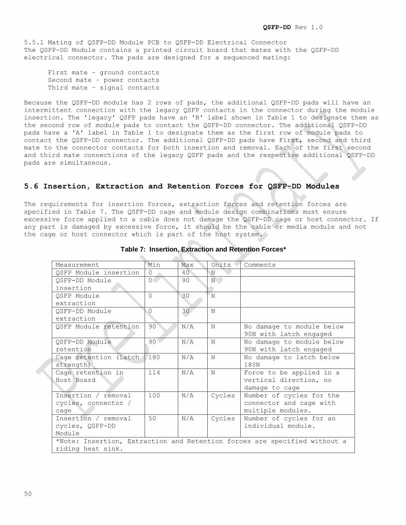
5.6 Insertion, Extraction and Retention Forces for QSFP-DD Modules
The requirements for insertion forces, extraction forces and retention forces are
specified in Table 7. The QSFP-DD cage and module design combinations must ensure
excessive force applied to a cable does not damage the QSFP-DD cage or host connector. If
any part is damaged by excessive force, it should be the cable or media module and not
the cage or host connector which is part of the host system.
Table 7: Insertion, Extraction and Retention Forces*
Measurement Min Max Units Comments
QSFP Module insertion 0 40 N
QSFP-DD Module
insertion
0 90 N
QSFP Module
extraction
0 30 N
QSFP-DD Module
extraction
0 30 N
QSFP Module retention 90 N/A N No damage to module below
90N with latch engaged
QSFP-DD Module
retention
90 N/A N No damage to module below
90N with latch engaged
Cage retention (Latch
strength)
180 N/A N No damage to latch below
180N
Cage retention in
Host Board
114 N/A N Force to be applied in a
vertical direction, no
damage to cage
Insertion / removal
cycles, connector /
cage
100 N/A Cycles Number of cycles for the
connector and cage with
multiple modules.
Insertion / removal
cycles, QSFP-DD
Module
50 N/A Cycles Number of cycles for an
individual module.
*Note: Insertion, Extraction and Retention forces are specified without a
riding heat sink.
QSFP-DD Rev 1.0
51
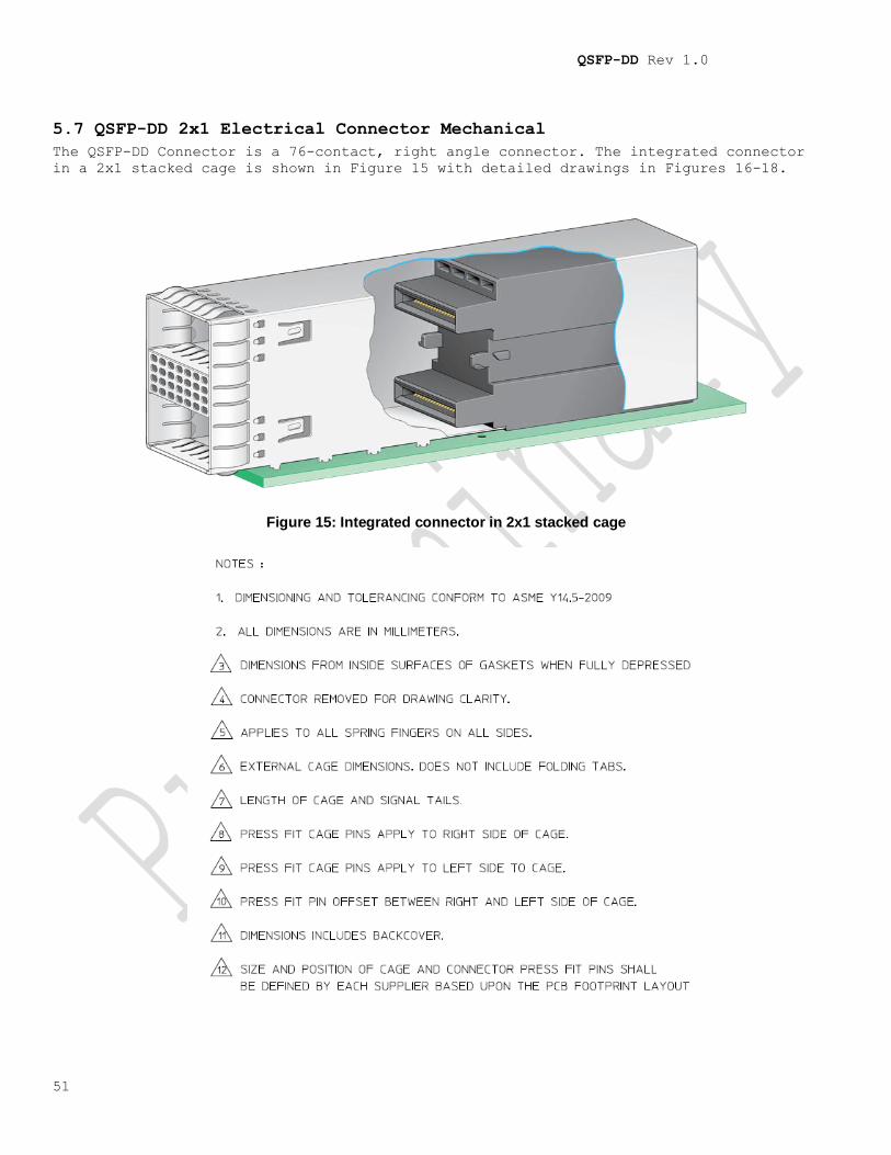
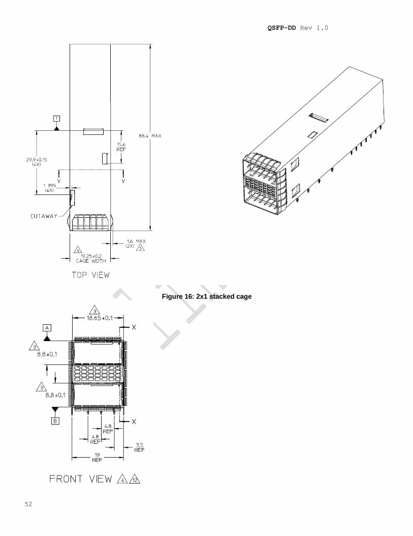
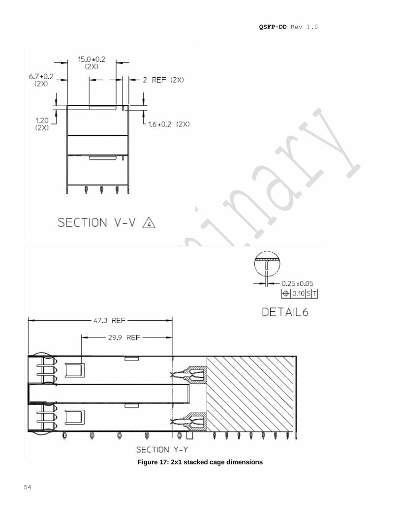
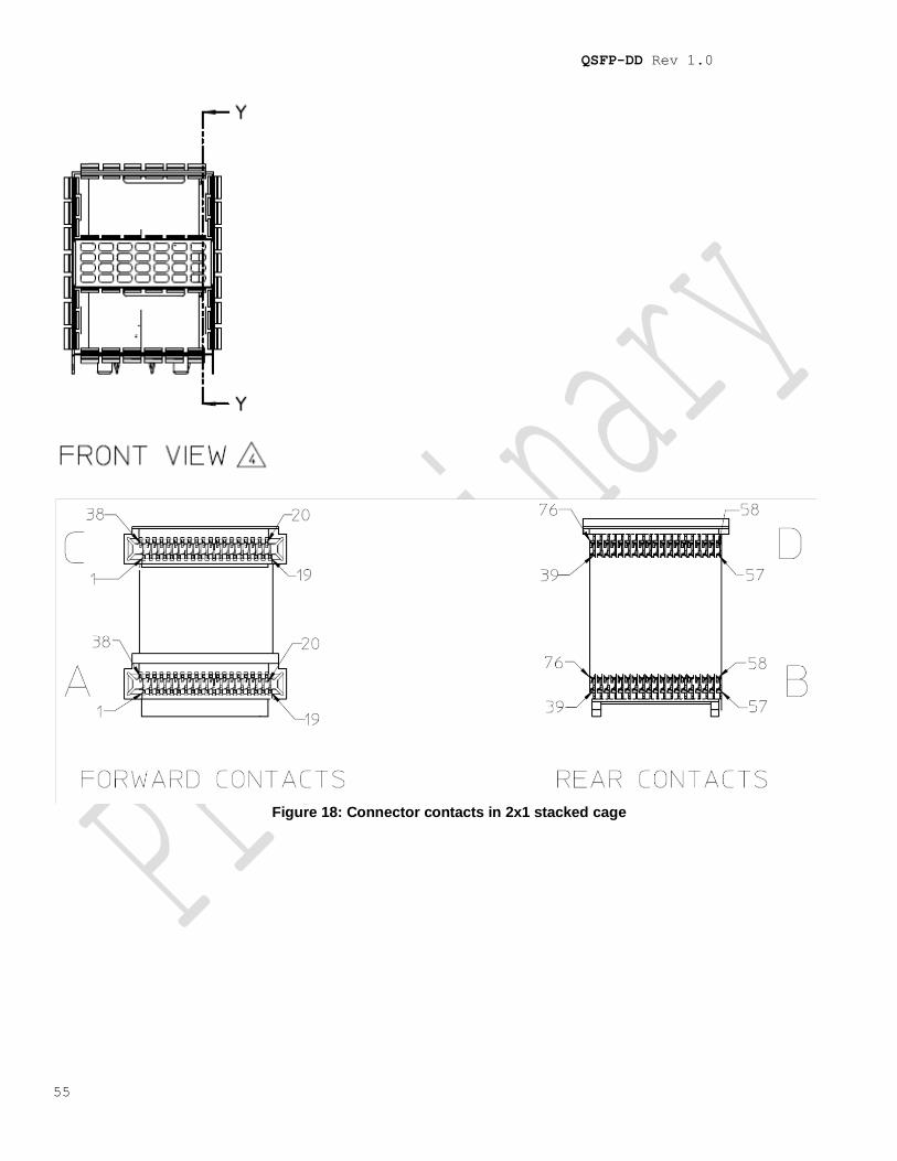
5.7 QSFP-DD 2x1 Electrical Connector Mechanical
The QSFP-DD Connector is a 76-contact, right angle connector. The integrated connector
in a 2x1 stacked cage is shown in Figure 15 with detailed drawings in Figures 16-18.
Figure 15: Integrated connector in 2x1 stacked cage
QSFP-DD Rev 1.0
52
Figure 16: 2x1 stacked cage

QSFP-DD Rev 1.0
53
QSFP-DD Rev 1.0
54
Figure 17: 2x1 stacked cage dimensions
QSFP-DD Rev 1.0
55
Figure 18: Connector contacts in 2x1 stacked cage
QSFP-DD Rev 1.0
56
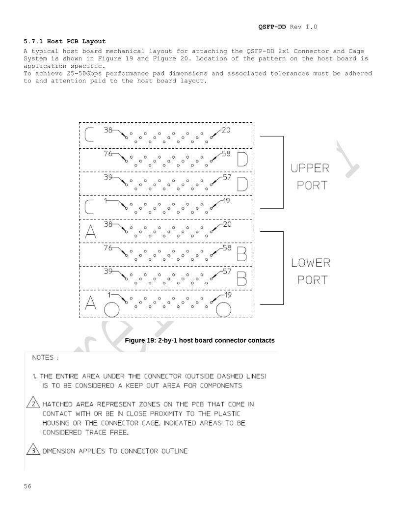
5.7.1 Host PCB Layout
A typical host board mechanical layout for attaching the QSFP-DD 2x1 Connector and Cage
System is shown in Figure 19 and Figure 20. Location of the pattern on the host board is
application specific.
To achieve 25-50Gbps performance pad dimensions and associated tolerances must be adhered
to and attention paid to the host board layout.
Figure 19: 2-by-1 host board connector contacts

QSFP-DD Rev 1.0
57
QSFP-DD Rev 1.0
58
QSFP-DD Rev 1.0
59
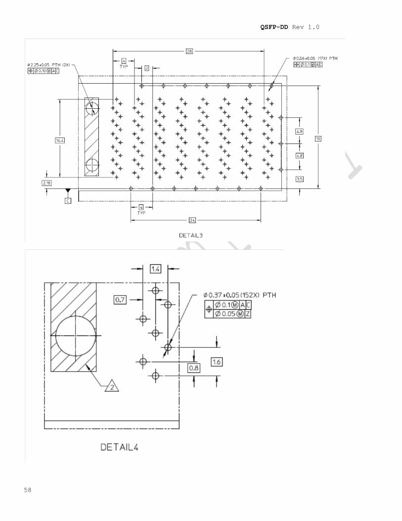
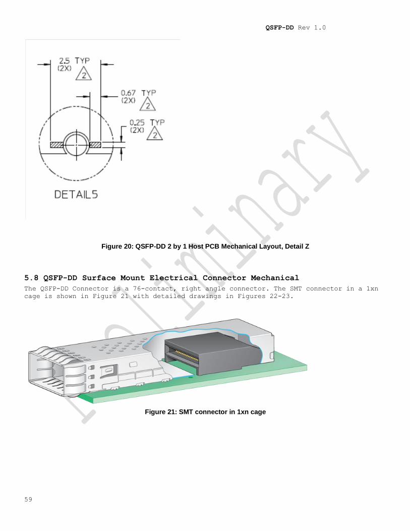
Figure 20: QSFP-DD 2 by 1 Host PCB Mechanical Layout, Detail Z
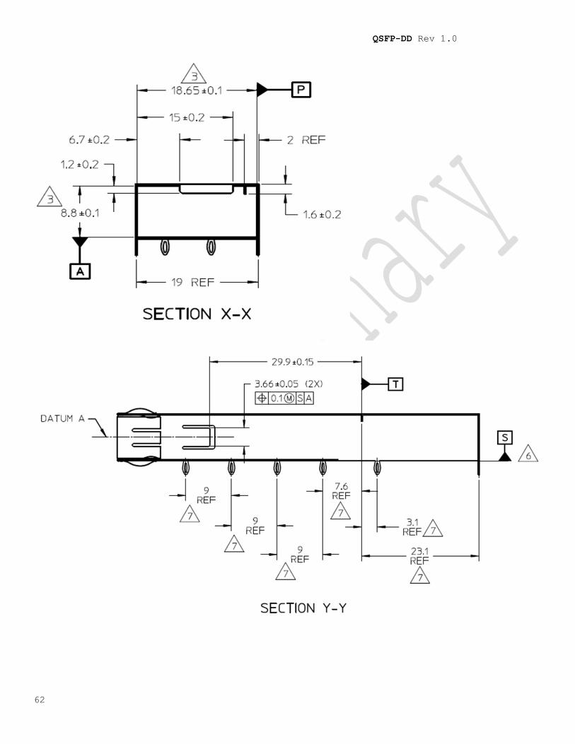
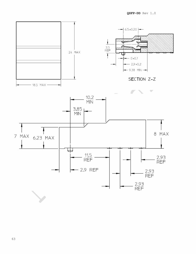
5.8 QSFP-DD Surface Mount Electrical Connector Mechanical
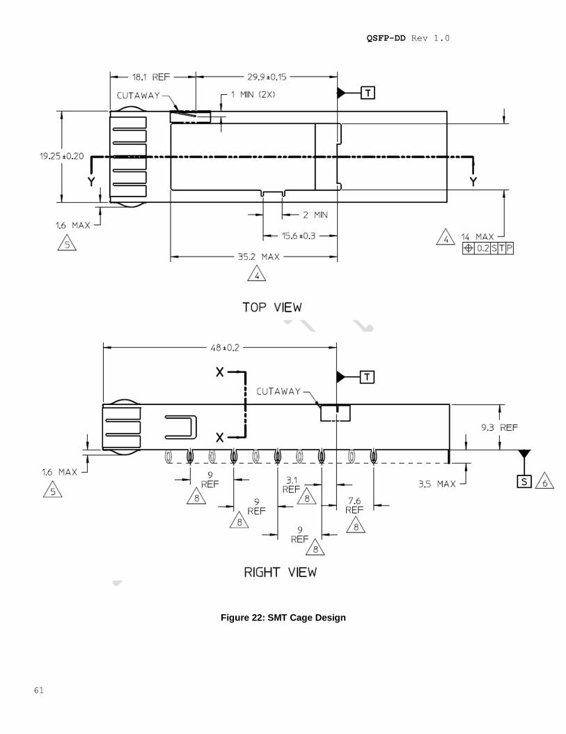
The QSFP-DD Connector is a 76-contact, right angle connector. The SMT connector in a 1xn
cage is shown in Figure 21 with detailed drawings in Figures 22-23.
Figure 21: SMT connector in 1xn cage
QSFP-DD Rev 1.0
60
QSFP-DD Rev 1.0
61
Figure 22: SMT Cage Design
QSFP-DD Rev 1.0
62
QSFP-DD Rev 1.0
63

QSFP-DD Rev 1.0
64
Figure 23: SMT Connector and Cage Design
QSFP-DD Rev 1.0
65
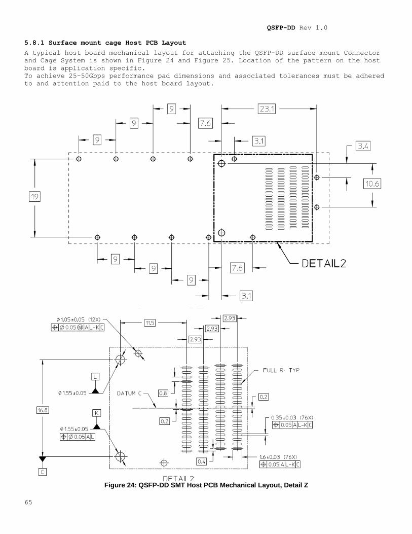
5.8.1 Surface mount cage Host PCB Layout
A typical host board mechanical layout for attaching the QSFP-DD surface mount Connector
and Cage System is shown in Figure 24 and Figure 25. Location of the pattern on the host
board is application specific.
To achieve 25-50Gbps performance pad dimensions and associated tolerances must be adhered
to and attention paid to the host board layout.
Figure 24: QSFP-DD SMT Host PCB Mechanical Layout, Detail Z

QSFP-DD Rev 1.0
66
5.9 Color Coding and Labeling of QSFP-DD Modules
An exposed feature of the QSFP-DD Module (a feature or surface extending outside of the
bezel) shall be color coded as follows:
Beige for 850nm
Blue for 1310nm
White for 1550nm
Each QSFP-DD Module shall be clearly labeled. The complete labeling need not be visible
when the QSFP-DD Module is installed and the bottom of the device is the recommended
location for the label. Labeling shall include:
Appropriate manufacturing and part number identification
Appropriate regulatory compliance labeling
A manufacturing traceability code
The label should also include clear specification of the external port characteristics
such as:
Optical wavelength
Required fiber characteristics
Operating data rate
Interface standards supported
Link length supported
The labeling shall not interfere with the mechanical, thermal or EMI features.

QSFP-DD Rev 1.0
67
5.10 Optical Interface
The QSFP-DD optical interface port shall be either a male MPO receptacle as specified in
IEC 61754-7 (see Figure 26a) or a dual LC as specified in IEC 61754-20 (see Figure 27a).
5.10.1 MPO Optical Cable connection
16 fiber MPO and 24 fiber MPO are shown in figure 26a. Note: 2 alignment pins are
present.
Aligned key (Type B) MPO patchcords should be used to ensure alignment of the signals
between the modules. The aligned key patchcord is defined in TIA-568 and shown in Figure
26b. The optical connector is orientated such that the keying feature of the MPO
receptacle is on the top.
Figure 25a: QSFP-DD Optical Receptacle and Channel Orientation for MPO connector
QSFP-DD Rev 1.0
68
Figure 25b: QSFP-DD 12 lane MPO Optical patchcord
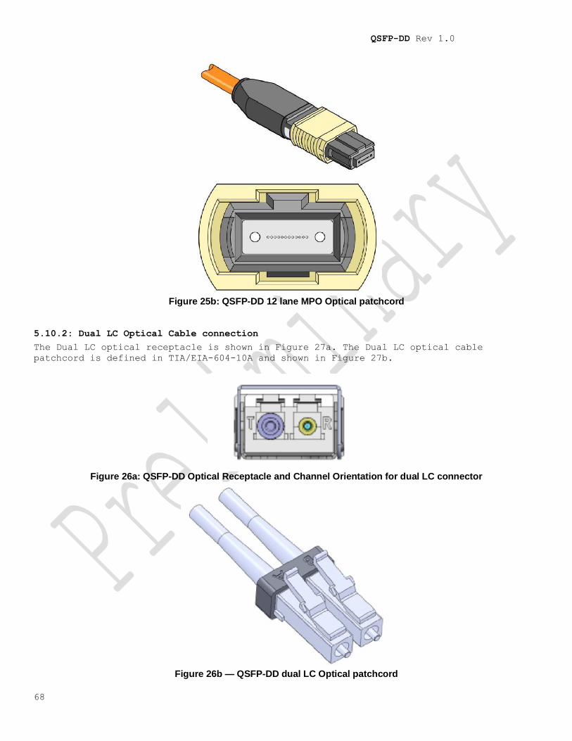
5.10.2: Dual LC Optical Cable connection
The Dual LC optical receptacle is shown in Figure 27a. The Dual LC optical cable
patchcord is defined in TIA/EIA-604-10A and shown in Figure 27b.
Figure 26a: QSFP-DD Optical Receptacle and Channel Orientation for dual LC connector
Figure 26b — QSFP-DD dual LC Optical patchcord
QSFP-DD Rev 1.0
69
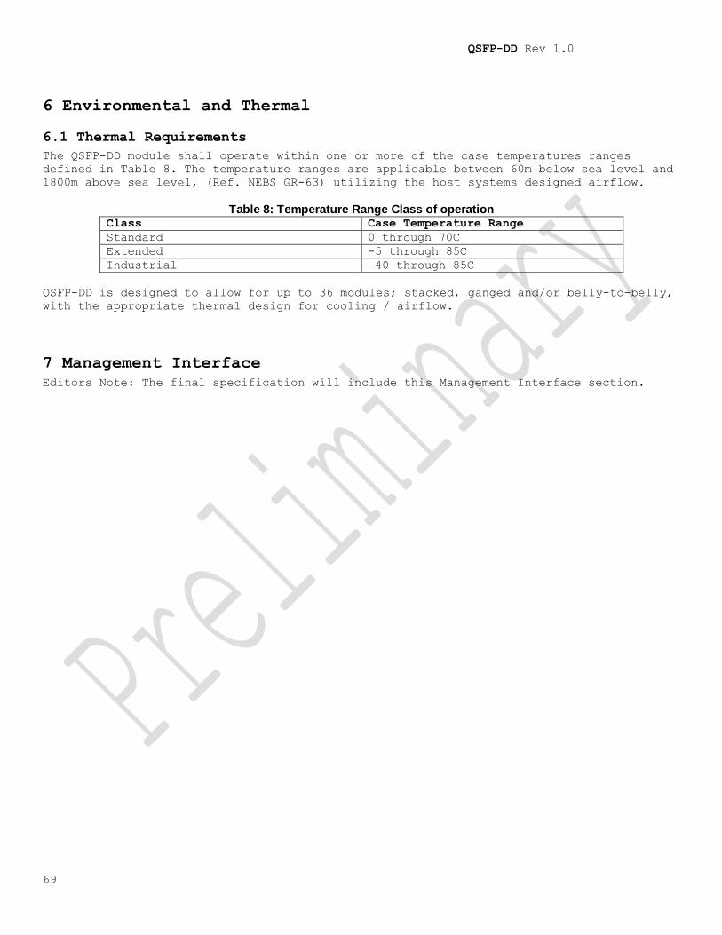
6 Environmental and Thermal
6.1 Thermal Requirements
The QSFP-DD module shall operate within one or more of the case temperatures ranges
defined in Table 8. The temperature ranges are applicable between 60m below sea level and
1800m above sea level, (Ref. NEBS GR-63) utilizing the host systems designed airflow.
Table 8: Temperature Range Class of operation Class Case Temperature Range
Standard 0 through 70C
Extended -5 through 85C
Industrial -40 through 85C
QSFP-DD is designed to allow for up to 36 modules; stacked, ganged and/or belly-to-belly,
with the appropriate thermal design for cooling / airflow.
7 Management Interface
Editors Note: The final specification will include this Management Interface section.