Embed Size (px)
Citation preview

SpecificationPCI eXtensions for Instrumentation
An Implementation of
Revision 1.0August 20, 1997


Rev. 8/20/97 © National Instruments Corporation iii
IMPORTANT INFORMATION
Copyright
© Copyright 1997 National Instruments Corporation. All rights reserved.
This document is copyrighted by National Instruments Corporation. Permission is granted to reproduce anddistribute this document in its entirety and without modification.
NOTICE
The PXI Specification is authored and copyrighted by National Instruments Corporation. The intent ofNational Instruments is for the PXI Specification to be an open industry standard supported by a widevariety of vendors and products. Vendors and users who are interested in developing PXI-compatibleproducts or services, as well as parties who are interested in working with National Instruments to furtherpromote PXI as an open industry standard are invited to contact National Instruments for furtherinformation.
National Instruments wants to receive your comments on this specification. Write to National Instruments,Attn: PXI Specification Committee, 6504 Bridge Point Parkway, Austin, TX 78730.
National Instruments makes no warranty of any kind with regard to this material, including, but not limitedto, the implied warranties of merchantability and fitness for a particular purpose. National Instruments shallnot be liable for errors contained herein or for incidental or consequential damages in connection with thefurnishing, performance, or use of this material.
Trademarks
LabVIEW™ and CVI™ are trademarks of National Instruments Corporation.
Product and company names are trademarks or trade names of their respective companies.

© National Instruments Corporation Rev. 8/20/97iv
PXI Specification Revision History
This section is an overview of the revision history of the PXI specification. Specific individualadditions/modifications to the document between revisions are denoted with diff marks, “|”, in the rightcolumn of a line of text for which the change applies.
Revision 1.0, August 20, 1997This is the first public revision of the PXI specification.

Rev. 8/20/97 © National Instruments Corporation v
Contents
1. Introduction ..................................................................................................................... 91.1. Objectives................................................................................................................. 91.2. Intended Audience and Scope ................................................................................ 101.3. Background and Terminology................................................................................ 101.4. Applicable Documents ........................................................................................... 11
2. PXI Architecture Overview........................................................................................... 132.1. Mechanical Architecture Overview........................................................................ 13
2.1.1. System Slot Location....................................................................................... 142.1.2. Additional Mechanical Features...................................................................... 152.1.3. Interoperability with CompactPCI .................................................................. 15
2.2. Electrical Architecture Overview........................................................................... 152.2.1. Peripheral Component Interconnect (PCI) Features........................................ 162.2.2. Local Bus......................................................................................................... 162.2.3. System Reference Clock ................................................................................. 172.2.4. Trigger Bus...................................................................................................... 172.2.5. Star Trigger...................................................................................................... 172.2.6. System Expansion with PCI-PCI Bridge Technology..................................... 18
2.3. Software Architecture Overview............................................................................ 192.3.1. Common Software Requirements ................................................................... 192.3.2. Virtual Instrument Software Standards ........................................................... 202.3.3. Other Software Requirements ......................................................................... 20
3. Mechanical Requirements ............................................................................................. 213.1. CompactPCI Mechanical Requirements ................................................................ 213.2. System Slot Location and Rules............................................................................. 213.3. Logos and Compatibility Glyphs............................................................................ 223.4. Environmental Testing ........................................................................................... 233.5. Cooling Specifications ........................................................................................... 24
3.5.1. Plug-in Module Requirements ........................................................................ 243.5.2. Chassis Requirements ..................................................................................... 24
3.6. Chassis and Module Grounding Requirements and EMI Guidelines..................... 253.7. Regulatory Requirements ....................................................................................... 25
3.7.1. Requirements for EMC ................................................................................... 253.7.2. Requirements for Electrical Safety.................................................................. 263.7.3. Particular Requirements for Chassis ............................................................... 26
4. Electrical Requirements ................................................................................................ 274.1. PXI Signal Groups.................................................................................................. 27
4.1.1. P1/J1: Signals .................................................................................................. 274.1.2. P2/J2: Signals .................................................................................................. 27
4.1.2.1. Signals from CompactPCI 64-Bit Connector Specification..................... 28System Slot........................................................................................................ 28

© National Instruments Corporation Rev. 8/20/97vi
Peripheral Module ............................................................................................. 29Backplane .......................................................................................................... 29
4.1.2.2. PXI Reserved and Bused Reserved Signals ............................................. 30System Slot........................................................................................................ 30Peripheral Slots ................................................................................................. 30Backplane .......................................................................................................... 30
4.1.2.3. Local Buses .............................................................................................. 30Peripheral Module ............................................................................................. 31Backplane .......................................................................................................... 32
4.1.2.4. Reference Clock: PXI_CLK10................................................................. 334.1.2.5. Trigger Bus............................................................................................... 34
Clock Transmission........................................................................................... 34PXI Trigger Protocols ....................................................................................... 34
PXI Asynchronous Trigger............................................................................ 34PXI Synchronous Trigger.............................................................................. 35
Backplane .......................................................................................................... 36Peripheral or System Module ............................................................................ 37
4.1.2.6. Star Trigger............................................................................................... 38Backplane .......................................................................................................... 39Peripheral Module ............................................................................................. 40
4.1.3. Electrical Guidelines for 6U............................................................................ 404.2. Connector Pin Assignments (J1/P1 and J2/P2)...................................................... 41
4.2.1. General Peripheral Slots.................................................................................. 414.2.2. System Slot...................................................................................................... 434.2.3. Star Trigger Slot .............................................................................................. 45
4.3. Chassis Power Supply Specifications..................................................................... 47
5. Software Frameworks and Requirements...................................................................... 495.1. Overview ................................................................................................................ 495.2. Motivation .............................................................................................................. 495.3. Framework Definition ............................................................................................ 505.4. Windows 95 System Framework ........................................................................... 50
5.4.1. Introduction ..................................................................................................... 505.4.2. Overview of the Framework............................................................................ 50
5.4.2.1. Controller Requirements .......................................................................... 505.4.2.2. PXI Peripheral Module Requirements ..................................................... 51
5.5. Windows NT System Framework .......................................................................... 525.5.1. Introduction ..................................................................................................... 525.5.2. Overview of the Framework............................................................................ 525.5.3. Controller Requirements ................................................................................. 52
5.5.3.1. PXI Peripheral Module Requirements ..................................................... 525.6. Support for Existing Instrumentation Standards .................................................... 535.7. System Implementation Issues ............................................................................... 54
5.7.1. System Configuration and Initialization Files................................................. 545.7.2. General .ini File Format .................................................................................. 55

Rev. 8/20/97 © National Instruments Corporation vii
5.7.3. PXI System Initialization (pxisys.ini) File ...................................................... 555.7.4. Chassis Initialization (chassis.ini) File............................................................ 575.7.5. Other Chassis Requirements ........................................................................... 58
Figures
Figure 1.1 The PXI Architecture..................................................................................... 10
Figure 2.1 PXI Peripheral Module Form Factors and Connectors.................................. 13Figure 2.2 Example of a 3U PXI System (Single Bus Segment) .................................... 14Figure 2.3 PXI and CompactPCI Interoperability ........................................................... 15Figure 2.4 PXI Local Bus Routing.................................................................................. 17Figure 2.5 PXI Trigger Architecture for Two Bus Segments ......................................... 19
Figure 3.1 Example of PXI Slot Designations for a Chassis .......................................... 22Figure 3.2 PXI Logo........................................................................................................ 23Figure 3.3 Star Trigger Slot Glyph.................................................................................. 23Figure 3.4 Cooling Airflow Direction in a PXI System.................................................. 24
Figure 4.1 PXI Asynchronous Trigger Timing ............................................................... 35Figure 4.2 PXI Synchronous Trigger Timing.................................................................. 35Figure 4.3 PXI Trigger Bus Termination ........................................................................ 36
Tables
Table 4.1 Local Bus Routings........................................................................................ 32Table 4.2 PXI Asynchronous Trigger Timing Parameters............................................. 35Table 4.3 PXI Synchronous Trigger Timing.................................................................. 36Table 4.4 DC Specifications .......................................................................................... 37Table 4.5 Pull-Up Resistor Values ................................................................................ 38Table 4.6 Type A, High Current Driver, AC Specifications.......................................... 38Table 4.7 Star Trigger Mapping..................................................................................... 39Table 4.8 PXI System Signal Groups ............................................................................ 41Table 4.9 Generic Peripheral Slot Pinout ...................................................................... 42Table 4.10 System Slot Pinout......................................................................................... 44Table 4.11 Star Trigger Slot Pinout ................................................................................. 46Table 4.12 5 V Backplane Power Requirements and Recommendations........................ 47Table 4.13 3.3 V Backplane Power Requirements and Recommendations..................... 47
Table 5.1 Development Environments Supported by PXI Modules underWindows 95................................................................................................... 51
Table 5.2 Development Environments Supported by PXI Modules underWindows NT.................................................................................................. 53
Table 5.3 Tag Line Descriptions.................................................................................... 56


Rev. 8/20/97 © National Instruments Corporation 9
1. IntroductionThis section describes the primary objectives and scope of the PCI eXtensions forInstrumentation (PXI) specification. It also defines the intended audience and listsrelevant terminology and documents.
1.1. ObjectivesPXI was created in response to the needs of a variety of instrumentation andautomation users who require ever increasing performance, functionality, andreliability from compact rugged systems that are easy to integrate and use. Existingindustry standards are leveraged by PXI to benefit from high component availabilityat lower costs. Most importantly, by maintaining software compatibility withindustry-standard personal computers, PXI allows industrial customers to use thesame software tools and environments with which they are familiar.
PXI leverages the electrical features defined by the widely adopted PeripheralComponent Interconnect (PCI) specification. It also leverages the CompactPCI formfactor, which combines the PCI electrical specification with rugged Eurocardmechanical packaging and high-performance connectors. This combination allowsCompactPCI and PXI systems to have up to seven peripheral slots versus four in adesktop PCI system. Systems with more expansion slots can be built by usingmultiple bus segments with industry-standard PCI-PCI bridges. For example, a13-slot PXI system can be built using a single PCI-PCI bridge. The PXI specificationadds electrical features that meet the high-performance requirements ofinstrumentation applications by providing triggering, local buses, and system clockcapabilities. PXI also offers two-way interoperability with CompactPCI products.
By implementing desktop PCI in a rugged form factor, PXI systems can leverage thelarge base of existing industry-standard software. Desktop PC users have access todifferent levels of software, from operating systems to low-level device drivers tohigh-level instrument drivers to complete graphical APIs. All of these software levelscan be used in PXI systems. PXI defines software frameworks (for MicrosoftWindows NT and Windows 95) for complete systems and requires appropriatedevice driver software for all PXI peripheral modules to ease system integration.Furthermore, PXI implements the Virtual Instrument Software Architecture (VISA).VISA is used to locate and communicate with serial, VXI, and GPIB peripheralmodules. PXI extends VISA beyond these interfaces to allow for the location andcontrol of PXI peripheral modules. This extension preserves the model forinstrumentation software that has been adopted by the instrumentation community.The result is a very powerful software commonality that spans PXI, CompactPCI,desktop PCI, VXI, GPIB, and other instrumentation architectures.
The diagram in Figure 1.1 summarizes the scope of the PXI specification bydepicting its mechanical, electrical, and software architectures.

© National Instruments Corporation Rev. 8/20/9710
PXI: PCI eXtensions for Instrumentation
MechanicalArchitecture
ElectricalArchitecture
PCI andCompactPCI
32/64 BitTransfers
33 MHz
InstrumentationFunctions
SoftwareArchitecture
Star Trigger
Reference Clock
Local Bus
Trigger Bus
CompactPCI
EuroCardPackaging
8 Slots
IECConnectors
PXI Additions
Env. Testing
Cooling
Defined SystemSlot Location
OperatingSystems
Windows 95
DriverSoftware
Windows NT
Language API
Graphical API
VISA
Driver Required
Figure 1.1 The PXI Architecture
1.2. Intended Audience and ScopeThis specification is organized with a top-down approach whereby generaldescriptions precede the more detailed specifications found deeper in the subsections.This structure is intended to serve the needs of a variety of audiences from productdevelopers to system integrators to end-users. Product developers may want tobecome familiar with all portions of this specification while end users may beinterested in only the feature set description and perhaps the summaries of how thesefeatures are implemented. The goal of this specification is to serve as the centralsource of information relevant to all users and providers of PXI compatible systems.
The first section of this specification describes the features that PXI systems canoffer and how these features can be applied to instrumentation. The subsequentsections cover the mechanical, electrical, and software requirements specific toimplementing PXI features.
1.3. Background and TerminologyThis section defines the acronyms and key words that are referred to throughout thisspecification. This specification uses the following acronyms:
API—Application Programming Interface
Eurocard—European Packaging Specifications (IEC 60297, IEEE 1101.1,IEEE 1101.10, IEEE 1101.11)
GPIB—General Purpose Interface Bus, IEEE 488
ISA—Industry Standard Architecture; desktop PC adapter board specification
PCI—Peripheral Component Interconnect; electrical specification defined byPCISIG
PCISIG—PCI Special Interest Group

Rev. 8/20/97 © National Instruments Corporation 11
PICMG —PCI Industrial Computer Manufacturers Group
PXI—PCI eXtensions for Instrumentation
VISA—Virtual Instrument Software Architecture
VITA —VMEbus International Trade Association
VME —Versa Module Europe; VMEbus specification governed by the VSO
VPP—VXI plug&play Specification
VSO—VITA Standards Organization
VXI —VME Extensions for Instrumentation
This specification uses several key words, which are defined as follows:
RULE: Rules SHALL be followed to ensure compatibility. A rule is characterizedby the use of the words SHALL and SHALL NOT.
RECOMMENDATION: Recommendations consist of advice to implementers thatwill affect the usability of the final module. A recommendation is characterized bythe use of the words SHOULD and SHOULD NOT.
PERMISSION: Permissions clarify the areas of the specification that are notspecifically prohibited. Permissions reassure the reader that a certain approach isacceptable and will cause no problems. A permission is characterized by the use ofthe word MAY.
OBSERVATION: Observations spell out implications of rules and bring attentionto things that might otherwise be overlooked. They also give the rationale behindcertain rules, so that the reader understands why the rule must be followed.
MAY: A key word indicating flexibility of choice with no implied preference. Thisword is usually associated with a permission.
SHALL: A key word indicating a mandatory requirement. Designers SHALLimplement such mandatory requirements to ensure interchangeability and to claimconformance with the specification. This word is usually associated with a rule.
SHOULD: A key word indicating flexibility of choice with a strongly preferredimplementation. This word is usually associated with a recommendation.
1.4. Applicable DocumentsThis specification defines extensions to the base PCI and CompactPCI specificationsreferenced in this section. It is assumed that the reader has a thorough understandingof PCI and CompactPCI. The CompactPCI specification refers to several otherapplicable documents with which the reader may wish to become familiar. Thisspecification refers to the following documents directly:
• PCI Local Bus Specification, Rev. 2.1
• PICMG 2.0 R2.1 CompactPCI Specification

© National Instruments Corporation Rev. 8/20/9712
• VXI plug&play Specifications (VPP-3.x and VPP-7)
• Serialized IRQ Support for PCI Systems Specification, Rev. 6.0, September 1,1995, Compaq Computer et al.
• IEC 61326-1:1997, Electrical equipment for measurement, control, andlaboratory use—EMC requirements—Part I, General requirements, InternationalElectrotechnical Commission
• IEC 1010-1:1990 + A1:1992, Safety requirements for electrical equipment formeasurement, control, and laboratory use—Part 1, General requirements,International Electrotechnical Commission
• IEC 60068-1, Environmental testing, International Electrotechnical Commission
• Hardware Design Guide for Microsoft Windows 95, Microsoft Corporation
• PC 97 Hardware Design Guide, Microsoft Corporation

Rev. 8/20/97 © National Instruments Corporation 13
2. PXI Architecture OverviewThis section presents an overview of a PXI system’s features and capabilities bysummarizing the mechanical, electrical and software architectures defined by thisspecification.
2.1. Mechanical Architecture OverviewPXI supports the two form factors that are depicted in Figure 2.1. The 3U formfactor defines modules that are 100 by 160 mm (3.94 by 6.3 in.) and have twointerface connectors. J1 carries the signals required for the 32-bit PCI local bus andJ2 carries the signals for 64-bit PCI transfers and the signals for implementing PXIelectrical features. The 6U form factor defines modules that are 233.35 by 160 mm(9.19 by 6.3 in.) and may carry up to three additional connectors for future expansionof the PXI specification.
3U PXI
J2
J1
J2
J1
J3
J5
J4
6U PXI
64-Bit PCI andPXI Features
32-Bit PCI
64-Bit PCI andPXI Features
32-Bit PCI
PXI Reserved
PXI Reserved
PXI Reserved
Ejector/Injector
Figure 2.1 PXI Peripheral Module Form Factors and Connectors
Figure 2.2 presents an example of a typical PXI system to help illustrate thefollowing keywords (in italics). A PXI system is composed of a chassis thatsupports the PXI backplane and provides the means for supporting the systemcontroller module and the peripheral modules. The chassis must have onesystem slot and may have one or more peripheral slots. Any number ofcontroller expansion slots may be available to the left of the system slot. Theoptional star trigger controller, when used, must reside next to the systemcontroller module. If a star trigger controller is not used in a system, a peripheralmodule can be installed in the slot next to the system controller module. Thebackplane carries the interface connectors (P1, P2, ...) and provides theinterconnection between the controller and peripheral modules. A maximum of

© National Instruments Corporation Rev. 8/20/9714
seven peripheral modules can be used in a single PXI bus segment. PCI-PCIbridges can be used to add bus segments for additional expansion slots.
87654321
P2
P1
System ControllerModuleController
Expansion Slots
System Slot
Star Trigger Controlleror Peripheral Slot
Seven AvailablePeripheral Slots
Peripheral Modules Empty Slot
Backplane
Chassis
EjectorHandles
Figure 2.2 Example of a 3U PXI System (Single Bus Segment)
2.1.1. System Slot LocationPXI defines the system slot location to be on the left end of the PCI bus segment.This defined arrangement is a subset of the numerous possible configurationsallowed by CompactPCI (a CompactPCI system slot may be located anywhereon a backplane). Defining a single location for the system slot simplifiesintegration and increases the degree of compatibility between PXI controllersand chassis. Furthermore, the PXI specification requires that if necessary thesystem controller module should expand to the left into what are defined ascontroller expansion slots. Expanding to the left prevents system controllersfrom using up valuable peripheral slots.
PXI also defines the location of a star trigger controller slot that can accept aperipheral module or a special star trigger module that can provide individualtriggers to all other peripheral modules. The star trigger signals are routed fromthe star trigger slot to each peripheral slot on all PXI backplanes.

Rev. 8/20/97 © National Instruments Corporation 15
2.1.2. Additional Mechanical FeaturesAll mechanical specifications defined in PICMG 2.0 R2.1 (CompactPCISpecification) apply directly to PXI systems; however, PXI includes additionalrequirements that simplify system integration. Forced cooling in PXI chassis isrequired and the airflow direction is defined. Environmental testing for operatingand storage temperature ratings of all PXI products is required and must beclearly documented by suppliers.
2.1.3. Interoperability with CompactPCIInteroperability among PXI compatible products and standard CompactPCIproducts is a very important feature provided by this specification. ManyPXI-compatible systems will require components that do not implementPXI-specific features. For example, a user may want to use a standardCompactPCI network interface module in a PXI chassis. Likewise, some usersmay choose to use a PXI compatible module in a standard CompactPCI chassis.In these cases, the user will not be able to use PXI-specific functions but willstill be able to use the basic functions of the module. Note that interoperabilitybetween PXI-compatible products that use the J2 connector for PXI-definedsignals and other application-specific implementations of CompactPCI chassis(which may define other signal definitions for sub-buses on the P2 backplaneconnector) is not guaranteed. Of course, both CompactPCI and PXI leverage thePCI local bus, thereby ensuring software and electrical compatibility as depictedin Figure 2.3.
CompactPCIChassis
PXI PeripheralModule
CompactPCIPeripheral Module
PXI Chassis
Full PXI Feature Set
PCI Electrical and Software Compatibility
Figure 2.3 PXI and CompactPCI Interoperability
2.2. Electrical Architecture OverviewMany instrumentation applications require system timing capabilities that cannot bedirectly implemented across standard desktop computer backplanes such as ISA,PCI, or PCMCIA. PXI uses the standard PCI bus and adds specific signals forinstrumentation including bused trigger lines, slot-specific triggers, a dedicated
© National Instruments Corporation Rev. 8/20/9716
system clock, and slot-to-slot local buses to address the need for advanced timing,synchronization, and side-band communication.
2.2.1. Peripheral Component Interconnect (PCI) FeaturesPXI offers the same performance features defined by the desktop PCIspecification, with one notable exception. A PXI system can have up to eightslots per segment (one system slot and seven peripheral slots), whereas a desktopPCI system can have only five per segment (one motherboard or system slot andfour peripheral slots). The capability to have three additional peripheral slots isdefined in the CompactPCI specification upon which PXI draws. Otherwise, allthe features of PCI transfer into PXI:
• 33 MHz performance
• 32- and 64-bit data transfers
• 132 Mbytes/s (32-bit) and 264 Mbytes/s (64-bit) peak data rates
• System expansion via PCI-PCI bridges
• 3.3 V migration
• Plug and Play capability
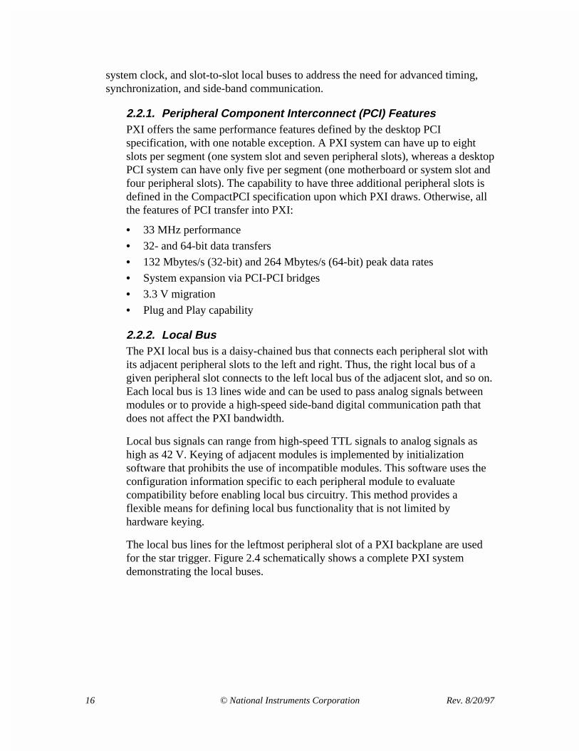
2.2.2. Local BusThe PXI local bus is a daisy-chained bus that connects each peripheral slot withits adjacent peripheral slots to the left and right. Thus, the right local bus of agiven peripheral slot connects to the left local bus of the adjacent slot, and so on.Each local bus is 13 lines wide and can be used to pass analog signals betweenmodules or to provide a high-speed side-band digital communication path thatdoes not affect the PXI bandwidth.
Local bus signals can range from high-speed TTL signals to analog signals ashigh as 42 V. Keying of adjacent modules is implemented by initializationsoftware that prohibits the use of incompatible modules. This software uses theconfiguration information specific to each peripheral module to evaluatecompatibility before enabling local bus circuitry. This method provides aflexible means for defining local bus functionality that is not limited byhardware keying.
The local bus lines for the leftmost peripheral slot of a PXI backplane are usedfor the star trigger. Figure 2.4 schematically shows a complete PXI systemdemonstrating the local buses.
Rev. 8/20/97 © National Instruments Corporation 17
Sys
tem
Con
trol
ler
Slo
t [1]
Sta
r T
rigge
r/P
erip
hera
l Slo
t [2]
Per
iphe
ral S
lot [
3]
Per
iphe
ral S
lot [
4]
Per
iphe
ral S
lot [
N-1
]
Per
iphe
ral S
lot [
N]
LocalBus
LocalBus
Star Triggers
PCI Arbitration and Clock Signals
LocalBus External
BackplaneInterface
Figure 2.4 PXI Local Bus Routing
2.2.3. System Reference ClockThe PXI 10 MHz system clock (PXI_CLK10) is distributed to all peripheralmodules in a system. This common reference clock can be used forsynchronization of multiple modules in a measurement or control system. ThePXI backplane specification defines implementation guidelines for PXI_CLK10.As a result, the low skew qualities afforded by this reference clock make it idealfor precise multimodule synchronization by using trigger bus protocols toqualify individual clock edges.
2.2.4. Trigger BusThe eight PXI bused trigger lines are highly flexible and can be used in a varietyof ways. For example, triggers can be used to synchronize the operation ofseveral different PXI peripheral modules. In other applications, one module cancontrol carefully timed sequences of operations performed on other modules inthe system. Triggers may be passed from one module to another, allowingprecisely timed responses to asynchronous external events that are beingmonitored or controlled. The number of triggers that a particular applicationrequires varies with the complexity and number of events involved.
2.2.5. Star TriggerThe PXI star trigger bus offers ultra-high performance synchronization featuresto users of PXI systems. The star trigger bus implements a dedicated trigger linebetween the first peripheral slot (adjacent to the system slot) and the otherperipheral slots. A star trigger controller can be installed in this slot and can beused to provide very precise trigger signals to other peripheral modules. Systemsthat do not require this advanced trigger can install any standard peripheral

© National Instruments Corporation Rev. 8/20/9718
module in this slot. Through the required use of line-length equalizationtechniques for routing the star triggers, PXI systems can meet demandingtriggering requirements for which bused triggers are not appropriate. Note thatthe star trigger can be used to communicate information back to the star triggercontroller, as in the case of reporting a slot’s status, as well as responding toinformation provided by the star trigger controller.
This trigger architecture for PXI gives two unique advantages in augmenting thebused trigger lines. The first advantage is a guarantee of a unique trigger line foreach module in the system. For large systems, this eliminates the need tocombine multiple module functions on a single trigger line or to artificially limitthe number of trigger times available. The second advantage is the low-skewconnection from a single trigger point. The PXI backplane defines specificlayout requirements such that the star trigger lines provide matched propagationtime from the star trigger slot to each module for very precise triggerrelationships between each module.
2.2.6. System Expansion with PCI-PCI Bridge TechnologyA PXI system can be built with more than one bus segment by using standardPCI-PCI bridge technology. The bridge device takes up one PCI load on each ofthe bus segments that it links together. Thus, a system with two bus segmentsoffers 13 expansion slots for PXI peripheral modules.
(2 bus segments) x (8 slots per segment) - (1 system controller slot)- (2 slots for PCI-PCI Bridge) = 13 available expansion slots
Similarly, a three-bus segment system would offer 19 expansion slots for PXIperipheral modules.
The trigger architecture defined by PXI has implications for systems withmultiple bus segments. The PXI trigger bus provides connectivity within a singlebus segment and does not allow physical connection to an adjacent bus segment.This maintains the high performance characteristics of the trigger bus and allowsmultisegment systems to partition instruments into logical groups. Multiplesegments may be logically linked by providing buffers between physicalsegments. The star trigger provides the means to independently access all 13peripheral slots in a two-segment system for applications in which a highnumber of instruments require synchronization and controlled timing.

Rev. 8/20/97 © National Instruments Corporation 19
Slo
t 1
Slo
t 2
Slo
t 3
Slo
t 7
Slo
t 8
Slo
t 9
Slo
t 10
Slo
t 16
SystemController
Star TriggerController
Bridge ControlsBus Segment 2
PXI Star Trigger
PXI Trigger Bus (Segment 1) PXI Trigger Bus (Segment 2)
PCI-PCIBridge
Figure 2.5 PXI Trigger Architecture for Two Bus Segments
2.3. Software Architecture OverviewLike other bus architectures, PXI defines standards that allow products from multiplevendors to work together at the hardware interface level. Unlike many otherspecifications, however, PXI defines software requirements in addition to bus-levelelectrical requirements, to further ease integration. These requirements include thesupport of standard operating system frameworks such as Windows NT andWindows 95 (WIN32) and the support of instrumentation software standardsdeveloped by the VXIplug&play Systems Alliance (VPP and VISA). Appropriatedrivers for all peripheral modules are also required. Clearly, the PXI softwarespecification is motivated by the benefits achieved through leveraging existingdesktop software technology.
2.3.1. Common Software RequirementsThe PXI specification presents software frameworks for PXI systems includingMicrosoft Windows NT and Windows 95. A PXI controller operating in eitherframework must support the currently available operating system and mustsupport future upgrades. The benefit of this requirement is that the controllertherefore also supports the most popular industry-standard applicationprogramming interfaces, such as Microsoft and Borland C++, Visual Basic,LabVIEW, and LabWindows®/CVI.
PXI also requires that all peripheral modules have device driver software thatruns in the appropriate framework. Hardware vendors for other industrial busesthat do not have software standards often do not provide any software drivers for

© National Instruments Corporation Rev. 8/20/9720
their devices. The customer is often given only a manual, which describes howto write software to control the device. The cost to the customer, in terms ofengineering effort to support these devices, can be enormous. PXI removes thisburden by requiring that manufacturers, rather than customers, develop thedriver software.
2.3.2. Virtual Instrument Software StandardsPXI systems are required to provide the VISA software standard as themechanism for locating and controlling GPIB, VXI, serial, and PXI instruments.Bringing the VISA standard to PXI preserves an instrumentation user’sinvestment in software. VISA provides the link from PXI to a VXI chassis andinstruments and to standalone GPIB and serial instruments. VISA provides astandard mechanism to locate, configure, and control PXI modules in a user’ssystem.
2.3.3. Other Software RequirementsPXI also requires that certain software components be made available byperipheral module and chassis vendors. Initialization files that define a system’sconfiguration and capabilities are required for PXI components. The systemsoftware uses this information to ensure proper configuration of a system. Forexample, this mechanism is used to identify whether or not adjacent peripheralmodules have a compatible local bus. If any information is missing, the local buscircuitry is not enabled and the functionality cannot be accessed.

Rev. 8/20/97 © National Instruments Corporation 21
3. Mechanical RequirementsThis section discusses the additional mechanical requirements for PXI systems. Itdiscusses the location of the system slot, the interoperability of the controller with thechassis, the PXI logo, environmental testing, cooling, grounding, and guidelines forminimizing electromagnetic interference (EMI).
3.1. CompactPCI Mechanical RequirementsBoth 3U (100 by 160 mm, or 3.94 by 6.3 in.) and 6U (233.35 by 160 mm, or 9.19 by6.3 in.) form factor modules can implement PXI features as defined in Section 4,Electrical Requirements.
RULE: All mechanical requirements defined in the CompactPCI specification(PICMG 2.0 R2.1) SHALL apply to 3U and 6U PXI compatible modules.
The following sections define additional mechanical requirements andrecommendations that are included to ease system integration.
3.2. System Slot Location and RulesAll CompactPCI and PXI compatible systems require a backplane/chassis and asystem controller module in the system slot. This requirement allows users to mixand match different controllers with different chassis. However, because theCompactPCI specification allows a system slot to be located anywhere relative toperipheral slots, the possibility for confusion and incompatibility exists. To addressthis problem the following rules must be followed for PXI-compatible systems:
RULE: The system slot SHALL be defined as the leftmost PXI slot in a basic singlebus segment PXI chassis/backplane. For documentation purposes this slot is countedas one controller slot.
RECOMMENDATION: If the system controller module requires more than oneslot width, it SHOULD extend to the LEFT of the system slot in full slot increments(one slot equals 20.32 mm, or 0.8 in.) into additional controller expansion slots.
OBSERVATION: These additional controller slots are for physical expansion of thesystem controller module only and cannot support peripheral modules. These slotsDO NOT have connectors that interface to the PCI bus routed on the backplane.
OBSERVATION: Extending the system slot module to the LEFT allows all PXIperipheral slots to be utilized.
RECOMMENDATION: The system controller module SHOULD NOT extend tothe RIGHT of the system slot into peripheral slots.

© National Instruments Corporation Rev. 8/20/9722
OBSERVATION: If a system controller module expands to the right, the number ofusable PXI peripheral slots is compromised and access to the star trigger slot iseliminated.
RULE: Every PXI system controller module SHALL clearly document how manycontroller expansion slots (to the left of the system slot) and peripheral slots itoccupies.
RULE: Every PXI chassis SHALL clearly document how many peripheral andcontroller expansion slots are available.
OBSERVATION: The two preceding rules help ensure that end users can easilydetermine whether a particular controller-chassis pair is compatible and how manyperipheral slots are left available.
Figure 3.1 depicts slot designations in a PXI system.
System Slot
Star TriggerController Slot
Three ControllerExpansion Slots
Seven Peripheral Slots
87654321
P2
P1
EjectorHandles
Figure 3.1 Example of PXI Slot Designations for a Chassis
3.3. Logos and Compatibility GlyphsRULE: A PXI chassis SHALL clearly mark each physical slot with a uniquenumber. The number SHALL be located within the compatibility glyph.
OBSERVATION: The preceding rule applies to a chassis with multiple bussegments as well as to a single-segment chassis.

Rev. 8/20/97 © National Instruments Corporation 23
RECOMMENDATION: Products claiming full compliance with the PXIspecification SHOULD use the PXI logo as defined below on either the front panelor the injector/ejector handle.
RULE: If the PXI logo is used, it SHALL NOT be altered in any way other thanscale. The logo SHALL NOT incorporate any additions.
Figure 3.2 shows the PXI logo. Logo artwork can be obtained by contacting NationalInstruments.
Figure 3.2 PXI Logo
PERMISSION: The PXI logo MAY be used as a substitute for the CompactPCIlogo defined in PICMG 2.0 R2.1. Additionally, a product MAY display both theCompactPCI logo and the PXI logo.
RULE: Modules and backplanes SHALL use the compatibility glyphs as defined inthe PICMG 2.0 R2.1 (CompactPCI specification).
RULE: Modules and backplanes SHALL use the glyph shown in Figure 3.3 (squareat 45°) for the star trigger slot/module. This slot is always located next to the systemslot. Because this slot can also support standard peripheral modules, the peripheralmodule glyph (circle) SHALL also be used for this slot.
Figure 3.3 Star Trigger Slot Glyph
3.4. Environmental TestingRULE: PXI chassis, system controller modules, and peripheral modules SHALL betested for storage and operating temperature ranges.
RECOMMENDATION: PXI chassis, system controller modules, and peripheralmodules SHOULD be tested for humidity, vibration, and shock.

© National Instruments Corporation Rev. 8/20/9724
RECOMMENDATION: All environmental testing SHOULD be carried outaccording to the procedures described in IEC 60068.
RULE: Test results and reports generated for environmental testing SHALL be madeavailable to end users of PXI systems. All manufacturers of PXI chassis, systemcontroller modules, and peripheral modules SHALL supply operating and storagetemperature ratings for their products.
RULE: If a manufacturer chooses to use environmental testing procedures other thanthose described in IEC 60068, then these procedures, in addition to the test resultsand reports, SHALL be documented and made available to the customer.
OBSERVATION: It is the system integrator’s responsibility to select modules andchassis appropriate for the application’s environmental requirements.
3.5. Cooling Specifications
3.5.1. Plug-in Module RequirementsRULE: Plug-in modules SHALL be designed to allow a suitable airflow pathfrom bottom to top as shown in Figure 3.4.
Figure 3.4 Cooling Airflow Direction in a PXI System
RULE: Plug-in module manufacturers SHALL document and make available tothe customer the nominal wattage generated by the module under normaloperating conditions.
3.5.2. Chassis RequirementsRULE: Chassis SHALL provide active cooling that flows from the bottom tothe top of a plugged-in module as shown in Figure 3.4.
RULE: Chassis manufacturers SHALL document and make available to thecustomer the maximum total wattage that a given chassis can dissipate and themaximum wattage dissipated for the worst-case slot. Furthermore, themanufacturer SHALL document and make available to the customer the specifictest procedure used to determine these wattage values.

Rev. 8/20/97 © National Instruments Corporation 25
3.6. Chassis and Module Grounding Requirements and EMIGuidelines
RULE: Chassis SHALL provide a direct (low-impedance) means for connecting thechassis ground to earth ground.
OBSERVATION: A grounding stud may be used to provide direct access to chassisground.
RECOMMENDATION: As defined in PICMG 2.0 R2.1, PXI modules SHOULDuse metalized shell connectors for EMI/RFI protection. The shell SHOULD beelectrically connected to the front panel through a low impedance path in accordancewith IEEE 1101.10.
RULE: As defined in PICMG 2.0 R2.1, PXI modules SHALL NOT connect chassisground through a low-impedance path to logic ground used onboard.
3.7. Regulatory RequirementsThe following standards assure uniform performance and international portability ofPXI systems and modules. Allowances are made for devices not intended forinternational sale. All regulatory compliance information must be clearlydocumented for the user. Subsequently issued standards or amendments to thesestandards shall apply.
3.7.1. Requirements for EMCRULE: Testing SHALL be performed, either by the manufacturer or acompetent laboratory, marked accordingly, and documented showingcompliance to the following EMC standard(s).
IEC 61326-1:1997, Electrical equipment for measurement, control, andlaboratory use—EMC requirements—Part I, General requirements1:
• Localized EMC standards may be substituted if sale and use are restrictedaccordingly.2
• Use current edition of IEC CISPR-11, Group 1, Class A or Class B Limits, at10 m.
• Continuous unmonitored operation is assumed unless otherwise specified bymanufacturer.
1 At the time of this writing, IEC 61326-1 was not yet normalized for CE Marking, but its first edition hasbeen published by the IEC as a bonafide standard. The ISM emission and generic immunity standards maybe substituted during any legally allowed transition period if documented accordingly.

© National Instruments Corporation Rev. 8/20/9726
3.7.2. Requirements for Electrical SafetyRULE: Testing SHALL be performed, either by a competent organization orqualified manufacturer, marked accordingly, and documented showingcompliance to the following electrical safety standard(s). Strictly extra lowvoltage (SELV) devices do not need formal agency testing, though the basicrequirements still apply, such as material flammability specified, DC poweroutputs fused or limited, and so on.
IEC 1010-1:1990 + A1:1992, Safety requirements for electrical equipment formeasurement, control, and laboratory use—Part 1, General requirements:
• IEC 950 and amendments are acceptable for applications restricted to theoffice use only.
• Localized safety standards may be substituted if sale and use are restrictedaccordingly. 2
3.7.3. Particular Requirements for ChassisRULE: Chassis manufacturers, or a designated party, SHALL demonstrate EMCcompliance with a commonly available controller. At minimum the controllerSHALL apply a 33 MHz clock to the backplane, or higher as the technologycommonly supports, unless the marketing and use of the chassis is restricted tospecific kinds of system controllers or platforms. A reasonably commonprocessor speed is sufficient for this test. The complete controller system,including hard drive, floppy drive, serial, parallel, keyboard, mouse, and videoports (as offered with the controller) will be exercised with typical peripherals.Filling remaining slots, if any, is not required. Special shielding or suppressionoptions, if used to achieve compliance, SHALL be documented and available tothe user.
RULE: The chassis SHALL be qualified for electrical safety as listedpreviously. Manufacturer claims of safety compliance are not sufficient withoutindependent verification and regular inspection by a competent agency.
2 The use of localized EMC or safety standards must be clearly documented for the benefit of the user. Thestandards used may include standards in force during legally allowed transitional periods of new standardsor amendments. Currently, manufacturer declarations must list all standards used for declaring complianceand conveniently meet this requirement when the declarations are included with the user documentation.

Rev. 8/20/97 © National Instruments Corporation 27
4. Electrical RequirementsThis chapter discusses the detailed electrical requirements for developing PXI-compatibleperipheral modules, controllers, and backplanes. It discusses all signals required for PXIsystems and their related implementation requirements. It also discusses appropriateconnector pinouts, power supply requirements, and 6U form factor implementationissues.
4.1. PXI Signal GroupsThis section details all the signals required for PXI systems, including those mappeddirectly from CompactPCI on P1/J1, the 64-bit signals duplicated on P2/J2, and thePXI-specific signals located on P2/J2. The PXI-specific signals include thoserequired for the trigger bus, the reference clock, the local buses, and the star trigger.
4.1.1. P1/J1: SignalsRULE: All signals on the P1/J1 connector of a PXI module and the matingP1 connector of a PXI backplane SHALL meet all the requirements of thePICMG 2.0 R2.1 specification (CompactPCI) for both peripheral modules andsystem modules.
RULE: Backplane devices that are not PCI-PCI bridges and peripheral slotsSHALL have their IDSEL lines connected to one of AD[25:31].
RULE: Backplane PCI-PCI bridges SHALL have their IDSEL lines connectedto AD lines other than AD[25:31].
To provide enhanced legacy ISA support, PXI allows for a serial interruptmechanism on the INTP or INTS line. This serial mechanism allows for ISAinterrupts to be generated on any peripheral module.
PERMISSION: The system controller module MAY use INTP or INTS as aserialized IRQ line for support of multiple legacy ISA interrupts from multiplemodules. Refer to revision 6.0 of the Serialized IRQ Support for PCI SystemsSpecification for details of the protocol.
OBSERVATION: If the system controller module uses INTP or INTS as aserialized IRQ, peripheral modules in the given PXI backplane will not be ableto successfully drive the serialized IRQ line (INTP or INTS) as a traditional ISAinterrupt.
4.1.2. P2/J2: SignalsThe PICMG 2.0 R2.1 (CompactPCI) specification defines an open pinout forP2/J2, which allows for custom back-panel I/O implementations. This pinoutallows sub-buses on the P2 section of the backplane.

© National Instruments Corporation Rev. 8/20/9728
The PXI back-panel I/O definition of signals on the P2/J2 connector consists ofsignals mapped from the CompactPCI 64-bit connector pinout and new signalsdefined by this specification. The only differences between the PXI pinout andthe CompactPCI 64-Bit connector pinout are on signals that are reserved or notused in the CompactPCI specification (PICMG 2.0 R2.1). Therefore, all modulesthat meet the requirements of the CompactPCI 64-bit specification will functionin a PXI system. Furthermore, all PXI modules will work in a system that meetsthe requirements of the CompactPCI 64-bit specification, but without thecomplete set of benefits of PXI.
4.1.2.1. Signals from CompactPCI 64-Bit ConnectorSpecification
To allow for applications that require higher bandwidth than 32-bit PCI canprovide, PXI has incorporated the pieces of the CompactPCI 64-bitspecification that are necessary to support 64-bit operation and has used theremaining resources for instrumentation. This section describes the signalsthat are mapped from the CompactPCI 64-bit specification. The remainingsignals are described in subsequent sections.
System SlotRULE: The following signals SHALL meet all the requirements of thePICMG 2.0 R2.1 specification for the 64-bit CompactPCI pinout on thesystem slot: GND, V(I/O), AD[32:63], C/BE[4:7]#, DEG#, FAL#,PRST#, SYSEN#, CLK[1:6], GNT[1:6]#, REQ[1:6]#, and the RSVpins.
RULE: The system slot interface in a PXI system SHALL be asdefined in the PICMG 2.0 R2.1 Specification (CompactPCI), except asnoted in the following rule:
RULE: The system controller module SHALL provide full support fora REQ#/GNT# pair to each slot in the given backplane (up to sevenslots). This support SHALL NOT be selectable. Instead, it SHALL beavailable to all slots in a system at once.
RECOMMENDATION: When using external logic on the systemcontroller module to convert one REQ/GNT pair to two pair, oneSHOULD make sure the timing meets all PCI setup/hold requirements.The unassertion of an additional grant SHOULD be in the same clockas that of the original grant so that the requesting master does not start acycle prematurely. A cycle can start prematurely if the system controllermodule grants the bus to a module while a cycle is pending and thenremoves the grant before the cycle is complete. It might be necessaryfor the system controller module to park the PCI bus to the system slot.

Rev. 8/20/97 © National Instruments Corporation 29
OBSERVATION: The PXI implementation of back-panel I/O uses thepins that are BRSV (bused reserved) in the CompactPCI 64-bit pinoutfor directly accessing PXI features on system modules.
Peripheral ModuleRULE: The following signals SHALL meet all the requirements of thePICMG 2.0 R2.1 specification for the 64-bit CompactPCI pinout on theperipheral slots: GND, V(I/O), AD[32:63], C/BE[4:7]#, DEG#, FAL#,and PRST#, and SYSEN#.
OBSERVATION: The PXI implementation of back-panel I/O uses thepins that are BRSV, CLK[1:6], GNT[1:6]#, REQ[1:6]#, and RSV in theCompactPCI 64-bit pinout for instrumentation features on peripheralmodules. Note that the CLK[1:4], GNT[1:6]# and REQ[1:6]# signalsare not implemented on CompactPCI peripheral modules and slots.
BackplaneRULE: The following signals SHALL meet all the requirements of thePICMG 2.0 R2.1 specification for the 64-bit CompactPCI pinout on thebackplane: GND, V(I/O), AD[32:63], C/BE[4:7]#, DEG#, FAL#, andPRST#, and SYSEN#.
RULE: As in the CompactPCI specification, the backplane SHALLroute CLK[1:4], GNT[1:6]#, and REQ[1:6]# from the system slot to theappropriate pins of the J1 connectors on the peripheral slots.
RULE: The backplane SHALL leave CLK5 and CLK6 of the systemslot disconnected.
RULE: The backplane SHALL leave all the RSV lines on the systemslot disconnected.
OBSERVATION: The PXI implementation of back-panel I/O uses thepins that are BRSV, CLK[1:6], GNT[1:6]#, REQ[1:6]#, and RSV(reserved) on peripheral slots and the BRSV pins on the system slot inthe CompactPCI 64-bit pinout for instrumentation features on thebackplane. The CLK[1:6], GNT[1:6]# and REQ[1:6]# signals are notimplemented on CompactPCI backplane peripheral slots.
OBSERVATION: The PXI implementation of back-panel I/O routesall of the bused reserved signals from the CompactPCI 64-bit pinout asbused signals on the PXI backplane. However, most of the signals arenot reserved in the PXI signal definition and are explained in theSection 4.1.2.5, Trigger Bus.
© National Instruments Corporation Rev. 8/20/9730
4.1.2.2. PXI Reserved and Bused Reserved Signals
System SlotThe following signals are reserved for future PXI use: PXI_BRSVA15,PXI_BRSVB4, PXI_RSVA22, PXI_RSVB22, PXI_RSVC22,PXI_RSVD22, and PXI_RSVE22.
RULE: A system controller module SHALL NOT connect to thePXI_BRSV signals.
Peripheral SlotsThe following signals are reserved for PXI use: PXI_BRSVA15,PXI_BRSVB4, PXI_RSVA22, PXI_RSVB22, PXI_RSVC22,PXI_RSVD22, and PXI_RSVE22.
RULE: A peripheral module SHALL NOT connect to the PXI_RSVsignals.
BackplaneThe following signals are reserved for PXI use: PXI_BRSVA15,PXI_BRSVB4, PXI_RSVA22, PXI_RSVB22, PXI_RSVC22,PXI_RSVD22, and PXI_RSVE22.
RULE: A backplane SHALL NOT connect to the PXI_RSV signals.
RULE: A backplane SHALL bus each PXI_BRSV signal to each slot.
OBSERVATION: PXI_BRSV and PXI_RSV signals are implementedon the backplane exactly like CompactPCI BRSV and RSV signals.
4.1.2.3. Local BusesPXI implements a daisy-chained local bus between adjacent peripheralmodules. The local bus is a user-definable bus (13 lines wide) that can beused for a wide variety of applications. The range of applications may varyfrom passing an analog signal between two modules to high-speed datamovement that does not affect the PXI bandwidth. For most slots, thefunctionality of the local bus is user-definable; however, there are specificimplementations that the PXI specification defines.
Note that the system controller module does not implement the local bus asit uses those pins for PCI arbitration and clocking functionality. The slotadjacent to the system slot uses its available local bus left signals for the startrigger functionality defined later. Similarly, the rightmost slot of the bushas no slot to its right; hence, the local bus right pins can either be unused or

Rev. 8/20/97 © National Instruments Corporation 31
routed for a chassis-specific implementation. One example ofchassis-specific implementation is routing the local bus to another adjacentPXI bus segment. The remainder of the slots can use the local bus for anyspecified purpose. Refer to Figure 2.4 for a diagram of local bus routing.
For system configuration purposes, the chassis configuration of the local buscan be determined by the initialization (.ini ) file of the chassis. The .inifile lists each slot and its location in the system. The system configurationsoftware uses this information to determine whether or not a system is puttogether properly.
The following rules apply to all implementations of the local bus:
Peripheral ModuleRULE: A peripheral module SHALL NOT drive more than ± 42 Vonto any local bus line.
RULE: A peripheral module SHALL NOT drive more than 200 mADC current into any local bus line.
PERMISSION: A peripheral module MAY connect its local bus left toits local bus right if passing the local bus to an additional module isrequired. This connection should be performed with caution becausethe length and/or characteristic impedance specifications of the localbus might be violated.
PERMISSION: On a peripheral module, a local bus signal MAY beconnected to ground.
OBSERVATION: The preceding permission allows local busimplementations to have improved grounding and/or shielding.
RULE: On a peripheral module, if a local bus signal is not connectedto ground, it SHALL power up in a high-impedance state. All local bussignals (except grounded ones) SHALL remain in a high-impedancestate until system configuration software has determined that the localbus signals are compatible with the chassis and other peripheralmodules in the system.
PERMISSION: A peripheral module MAY pull-up a local bus signalto V (I/O) to prevent an input from powering up in an unstable state.
RULE: Each peripheral module SHALL have a maximum inputleakage current of 100 µA on each local bus line.

© National Instruments Corporation Rev. 8/20/9732
BackplaneRULE: On each bus segment, a backplane SHALL routePXI_LBR[0:12] from each slot in column A of Table 4.1 to thePXI_LBL[0:12] of the corresponding slot in column B, provided thatboth slots exist on the bus segment.
Table 4.1 Local Bus Routings
A BIDSEL = 31 IDSEL = 30IDSEL = 30 IDSEL = 29IDSEL = 29 IDSEL = 28IDSEL = 28 IDSEL = 27IDSEL = 27 IDSEL = 26IDSEL = 26 IDSEL = 25
RULE: The backplane SHALL NOT make any other local busroutings.
OBSERVATION: There is no local bus connection to the system slot.
RULE: The backplane SHALL NOT provide any termination orbuffering of local bus signals. Each signal SHALL be implemented as adirect connection between adjacent peripheral slots.
RULE: The backplane SHALL NOT route the local bus between twobus segments.
RULE: Bus segment boundaries SHALL be documented.
OBSERVATION: Documenting bus segment boundaries allows usersto optimize systems by grouping boards that frequently talk to eachother on the same segment. It also allows users to know when adjacentphysical slots do not have a local bus connection.
RULE: The signal length of local bus signals between slots SHALL beless than 3 in. and SHALL be matched within 1 in. between all localbus traces. The characteristic impedance of each trace SHALL be65 Ω ± 10%.
PERMISSION: A slot at the end of a PXI segment or next to thesystem slot has one local bus that is not routed to another peripheralslot. The backplane MAY route these local buses for other uses.
Rev. 8/20/97 © National Instruments Corporation 33
RULE: A star trigger slot SHALL NOT implement a local bus left.Instead, the remaining pins SHALL be routed to support the startriggers.
RULE: If a chassis implements an external backplane interface withthe local bus right of a slot at the end of a PXI segment, it SHALL bethe highest numbered slot in the chassis.
OBSERVATION: A chassis will have at most one slot with anexternal backplane interface.
4.1.2.4. Reference Clock: PXI_CLK10The PXI backplane is responsible for providing a common reference clockfor synchronization of multiple modules in a measurement or controlsystem. The variable frequency of the PCI system clock limits its usefulnessin this application. PXI_CLK10 is a 10 MHz clock provided independentlyto each peripheral slot. PXI_CLK10 can be used to run multiple modules insynchronization from a common reference. The low skew qualities make itideal for qualifying trigger protocols.
RULE: The PXI_CLK10 provided by the backplane SHALL be a 10 MHzTTL signal. Its accuracy SHALL be ± 100 ppm or better over the specifiedoperating temperature and time.
OBSERVATION: Because of drift over time, the oscillator chosen MAYneed to be 50 ppm accurate or better to meet the requirement of thepreceding rule.
RULE: The PXI_CLK10 signal SHALL have a 50% ± 5% duty cycle whenmeasured at the 2.0 V transition point.
RULE: The clock to each peripheral slot SHALL be driven by anindependent buffer that has a source impedance matched to the backplane.
RULE: The backplane SHALL provide for a skew of less than 1 ns betweenslots.
RECOMMENDATION: A backplane SHOULD allow PXI_CLK10 to bederived from an external source to allow for a more accurate reference.
OBSERVATION: The star trigger slot has defined a pin for providing anexternal clock.
RULE: If the PXI_CLK10 is switched between sources, the minimum pulsewidth created SHALL be no less than 30 ns and the minimum time betweensuccessive edges of the same polarity SHALL be no less than 80 ns.

© National Instruments Corporation Rev. 8/20/9734
OBSERVATION: The preceding rule is intended to prevent a statemachine from being corrupted by glitches in the clock during transition.
4.1.2.5. Trigger BusThe PXI trigger bus provides intermodule synchronization andcommunication. The trigger bus lines can be used for trigger or clocktransmission. A few standard triggering protocols are defined to facilitateinteroperability, but use of the trigger bus is not limited to the definedprotocols. The PXI trigger bus lines may be used as general purposeintermodule bused lines using other manufacturer-defined protocols.
The PXI trigger bus consists of the following eight signals:
PXI_TRIG[0:7]
Clock TransmissionVariable frequency clock transmission allows multiple modules toshare a timebase that is not a derivative of the PXI_CLK10. Forexample, two data acquisition modules using a 44.1 kS/s CD audiosampling rate could share a clock that is a multiple of the 44.1 kHz.Type A drivers, defined later, prevent degradation of the clock jitterover the bused transmission medium.
PERMISSION: PXI_TRIG[0:7] MAY be used for variable frequencyclock transmission.
RECOMMENDATION: To facilitate interoperability between sourcesand receivers of a variable frequency clock, PXI_TRIG[7] SHOULD beused to source and receive such clocks.
PXI Trigger ProtocolsSome standard protocols are defined in the following sections.
PXI Asynchronous Trigger
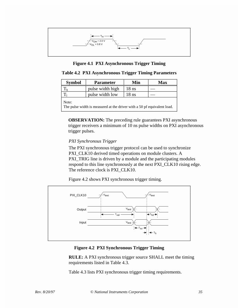
The PXI asynchronous trigger protocol is a single-line broadcasttrigger. Figure 4.1 and Table 4.2 show the timing parameters.
RULE: A PXI asynchronous trigger source SHALL meet the timingrequirements listed in Table 4.2.
Rev. 8/20/97 © National Instruments Corporation 35
TH
VOH = 2.0 VVOL = 0.8 V
TL
Figure 4.1 PXI Asynchronous Trigger Timing
Table 4.2 PXI Asynchronous Trigger Timing Parameters
Symbol Parameter Min MaxTh pulse width high 18 ns —Tl pulse width low 18 ns —
Note:The pulse width is measured at the driver with a 50 pf equivalent load.
OBSERVATION: The preceding rule guarantees PXI asynchronoustrigger receivers a minimum of 10 ns pulse widths on PXI asynchronoustrigger pulses.
PXI Synchronous Trigger
The PXI synchronous trigger protocol can be used to synchronizePXI_CLK10 derived timed operations on module clusters. APXI_TRIG line is driven by a module and the participating modulesrespond to this line synchronously at the next PXI_CLK10 rising edge.The reference clock is PXI_CLK10.
Figure 4.2 shows PXI synchronous trigger timing.
PXI_CLK10
Output
Input
Tval Thd
Th
Tsu
Vtest
Vtest
Vtest Vtest
Figure 4.2 PXI Synchronous Trigger Timing
RULE: A PXI synchronous trigger source SHALL meet the timingrequirements listed in Table 4.3.
Table 4.3 lists PXI synchronous trigger timing requirements.

© National Instruments Corporation Rev. 8/20/9736
Table 4.3 PXI Synchronous Trigger Timing
Symbol Parameter Min MaxThd Output hold time from
PXI_CLK102 ns —
Tval Output signal valid fromPXI_CLK10
— 65 ns
Tsu Input set up time to PXI_CLK10 23 ns —Th Input hold time from
PXI_CLK100 ns —
Note:Minimum times are measured with 0 pf equivalent load. Maximum times aremeasured with 50 pf equivalent load.
OBSERVATION: The output signal valid timing from PXI_CLK10allows either rising or falling edges of PXI_CLK10 to be used forsourcing PXI synchronous triggers.
BackplaneRULE: For each PXI segment in a PXI chassis, the PXI chassisSHALL bus the PXI_TRIG[0:7] signal to each PXI slot (system andperipheral) in that segment. A chassis SHALL NOT directly connectPXI_TRIG buses from different PXI segments. If a system slot controlsmultiple PXI segments, it SHALL NOT directly connect PXI triggerbuses from different segments.
OBSERVATION: Trigger buses from multiple segments arephysically disconnected to maintain signal integrity and allow forincident wave switching of Type A trigger drivers. However, the busesmay be logically connected by buffering the signals between segments.
RULE: PXI_TRIG[0:7] SHALL be fast Schottky diode terminated atboth ends of the bus segment on the backplane to + 5 V and ground asshown in Figure 4.3.
+5 V
PXI_TRIG
Figure 4.3 PXI Trigger Bus Termination

Rev. 8/20/97 © National Instruments Corporation 37
RULE: The unloaded characteristic impedance for the backplane Zl,min
SHALL be 75 Ω ± 10% using a stripline transmission line geometry.
OBSERVATION: The higher backplane impedance lowers the driverstrength requirements for incident wave switching.
RULE: The signal trace lengths of PXI trigger bus signals SHALL beless than 10 in. and matched within 1 in. between all trigger bus signals.
Peripheral or System ModuleRULE: Printed circuit board trace lengths for PXI trigger bus signalsSHALL be less than or equal to 1.5 in.
PERMISSION: A PXI module (system or peripheral) MAY leave anynumber of PXI trigger bus signals unconnected.
RECOMMENDATION: The following recommendations improveinteroperability between modules using the PXI trigger bus. Fortriggering applications, if a PXI module (system or peripheral) connectsto a subset of the PXI trigger signals, it SHOULD connect toPXI_STAR and PXI_TRIG[0:n-2] where n is the number of triggerlines on the peripheral module. For sourcing or receiving clocks,PXI_TRIG[7] SHOULD be used.
RULE: Upon power up, the PXI_TRIG[0:7] lines and drivers SHALLremain in a high impedance state until configured by software.
RULE: PXI_TRIG[0:7] I/O buffers SHALL be compliant with the DCspecifications listed in Table 4.4.
Table 4.4 DC Specifications
Symbol Parameter Condition Min Max NotesVih Input High Voltage — 2.0 V Vcc + 0.5 V 1Vil Input Low Voltage — -0.5 V 0.8 V —Il Leakage Current 0 < Vin < Vcc — ± 70 µA 1, 2Voh Output High Voltage Iout = - 2 mA 2.4 V — —Vol Output Low Voltage Iout = 4 mA — 0.55 V —Cpin Input, Output,
Bidirectional PinCapacitance
— — 10 pf —
Notes:1. Vcc refers to the 5 V power supply rail.2. Leakage current includes output leakage for bidirectional buffers in a high-impedance state.

© National Instruments Corporation Rev. 8/20/9738
OBSERVATION: The DC specifications are met by 5 V tolerantLVTTL-compatible I/O buffers.
PERMISSION: To prevent floating inputs, PXI_TRIG[0:7] lines usedon a PXI module (system or peripheral) MAY be pulled up on themodule with a pull-up resistance whose value is shown in Table 4.5.
Table 4.5 Pull-Up Resistor Values
Signaling Rail Rmin Rmax5 V 11 kΩ [Vccmin - Vx]/[Iih]*3.3 V 19 kΩ [Vccmin - Vx]/[Iih]*
* Vx = 2.4 V, which is the desired voltage on the bus in a non-drivenstate, and Iih is the maximum leakage current for the device buffer.
RECOMMENDATION: Type A drivers SHOULD be used for clocktransmission over the PXI trigger bus. Type A drivers are capable ofincident wave switching on rising edges, preventing jitter degradationdue to transmission line effects. Refer to Table 4.6 for Type A driverspecifications.
Table 4.6 Type A, High Current Driver, AC Specifications
Symbol Parameter Condition Min MaxVsoh(AC) Switching voltage high 2.3 V —Ioh(AC) High source current @Vsoh(AC) 75 mA —
RECOMMENDATION: Intermediate voltage levels (Vol ≤ V ≤ Voh)may be present on the trigger bus. Schmitt trigger inputs SHOULD beused to guard against sensing multiple transitions on edge-sensitiveinputs when the voltage on the bus is at intermediate levels due totransmission line effects on the bus.
RECOMMENDATION: Rising edges SHOULD be used as activeedges in asynchronous trigger protocols.
4.1.2.6. Star TriggerIn addition to the bused PXI triggers, the PXI bus has included anindependent trigger (PXI_STAR) for each slot that is oriented in a starconfiguration from the star trigger slot. The star trigger slot is adjacent tothe system slot and uses the 13 left local bus signals as the star triggers. Thisallows a single star trigger slot to control or monitor triggers in two PCI bussegments. In systems with more than two PCI segments, one star trigger slotis designated for two bus segments.

Rev. 8/20/97 © National Instruments Corporation 39
The PXI specification does not specify the functionality of the star triggerslot module or even require that the system be constructed with a star triggermodule. Typical uses would include triggering multiple modulesindependently with low skew, monitoring a trigger from peripheral slots,and routing triggers between slots. One star trigger slot pin is dedicated toallow an external 10 MHz frequency standard to be routed as PXI_CLK10.
BackplaneRULE: Slot 2 in a chassis SHALL be a star trigger slot.
RULE: A chassis SHALL NOT have more than one star trigger slot.
OBSERVATION: The star trigger slot may also be used as a genericperipheral slot with the exception that the left side local bus isunavailable because these pins connect to the star triggers. The startrigger slot does not have a PXI_STAR; instead, the pin in the startrigger slot is used for an external frequency reference.
RULE: The PXI backplane SHALL route the signals from the startrigger slot to each peripheral slot according to Table 4.7, with a traceimpedance of 65 Ω ± 10%. The mapping of the connections isdescribed in the chassis.ini file.
Table 4.7 Star Trigger Mapping
Star Trigger Signal Physical Peripheral SlotPXI_STAR0 3PXI_STAR1 4PXI_STAR2 5PXI_STAR3 6PXI_STAR4 7PXI_STAR5 8PXI_STAR6 9PXI_STAR7 10PXI_STAR8 11PXI_STAR9 12PXI_STAR10 13PXI_STAR11 14PXI_STAR12 15
RULE: The PXI_STAR line lengths SHALL be matched inpropagation delay to within 1 ns, and the delay from the star trigger slotto each peripheral module SHALL NOT exceed 5 ns.

© National Instruments Corporation Rev. 8/20/9740
Peripheral ModuleRULE: The driver of PXI_STAR, which may be the star triggermodule or a peripheral module, SHALL have a source impedance of65 Ω ± 10% to match the backplane impedance.
RULE: When a peripheral module or star trigger controller drives aPXI_STAR, the signaling levels SHALL NOT exceed 5 V.
RULE: A peripheral module SHALL NOT drive its PXI_STAR whenreset.
PERMISSION: A peripheral module MAY pull-up the PXI_STARsignal to prevent an unstable input.
RULE: The leakage current of a peripheral module connected toPXI_STAR SHALL NOT exceed 650 µA.
OBSERVATION: The same trigger protocols defined for the PXI TTLtrigger bus MAY be used on the PXI_STAR signals.
PERMISSION: The PXI_CLK10_IN signal of the star trigger slotMAY be used to provide an external 10 MHz reference forPXI_CLK10.
RULE: A module in the star trigger slot SHALL NOT drive thePXI_STAR/CLK10_IN signal, except to provide a reference forPXI_CLK10.
OBSERVATION: The presence of a periodic signal on thePXI_CLK10_IN signal MAY be used to indicate that an externalreference is to be used.
4.1.3. Electrical Guidelines for 6ULarger 6U size modules are desirable for the extra module space and possibly forfuture additional functionality that can be provided through the J3, J4, and J5connectors. In many cases, the extra space on a 6U module is needed only forextra circuitry, and the module requires only the J1 and J2 connectors for PXI.J3, J4, and J5 are reserved for future revisions of the PXI specification.
RULE: 6U PXI peripheral modules SHALL implement only J1 and J2. J3, J4,and J5 SHALL NOT be loaded on 6U peripheral modules.

Rev. 8/20/97 © National Instruments Corporation 41
4.2. Connector Pin Assignments (J1/P1 and J2/P2)To help in reviewing the tables in this section and locating the appropriatespecification for signal requirements, Table 4.8 lists all signals alphabetically byoriginal specification (PXI, CompactPCI, or PCI).
Table 4.8 PXI System Signal Groups
System SignalsPXI PXI_BRSV
PXI_CLK10
PXI_CLK10_IN
PXI_LBL[0:12]
PXI_LBR[0:12]
PXI_RSV
PXI_STAR
PXI_STAR[0:12]
PXI_TRIG[0:7]
CompactPCI BRSV
CLK[0:6]
DEG#
ENUM#
FAL#
GNT#[0:6]
INTP
INTS
PRST#
REQ#[0:6]
RSV
SYSEN#
PCI ACK64#
AD[0:63]
C/BE[0:7]#
CLK
DEVSEL#
FRAME#
GND
GNT#
IDSEL
INTA#
INTB#
INTC#
INTD#
IRDY#
LOCK#
M66EN
PAR
PAR64
PERR#
REQ#
REQ64#
RST#
SBO#
SDONE
SERR#
STOP#
TCK
TDI
TDO
TMS
TRDY#
TRST#
V(I/O)
3.3 V
5 V
+12 V
-12 V
4.2.1. General Peripheral SlotsTable 4.9 gives the peripheral slot pinout for the J1 and J2 connector.PXI-specific signals are shown in bold.
RULE: Peripheral modules and backplane peripheral slots SHALL use thepinout in Table 4.9.

© National Instruments Corporation Rev. 8/20/9742
Table 4.9 Generic Peripheral Slot Pinout
22 GND PXI_RSVA22 PXI_RSVB22 PXI_RSVC22 PXI_RSVD22 PXI_RSVE22 GND21 GND PXI_LBR0 GND PXI_LBR1 PXI_LBR2 PXI_LBR3 GND20 GND PXI_LBR4 PXI_LBR5 PXI_LBL0 GND PXI_LBL1 GND19 GND PXI_LBL2 GND PXI_LBL3 PXI_LBL4 PXI_LBL5 GND18 GND PXI_TRIG3 PXI_TRIG4 PXI_TRIG5 GND PXI_TRIG6 GND P217 GND PXI_TRIG2 GND PRST# PXI_STAR PXI_CLK10 GND /16 GND PXI_TRIG1 PXI_TRIG0 DEG# GND PXI_TRIG7 GND J215 GND PXI_BRSVA15 GND FAL# PXI_LBL6 PXI_LBR6 GND14 GND AD[35] AD[34] AD[33] GND AD[32] GND13 GND AD[38] GND V(I/O) AD[37] AD[36] GND C12 GND AD[42] AD[41] AD[40] GND AD[39] GND O11 GND AD[45] GND V(I/O) AD[44] AD[43] GND N10 GND AD[49] AD[48] AD[47] GND AD[46] GND N9 GND AD[52] GND V(I/O) AD[51] AD[50] GND E8 GND AD[56] AD[55] AD[54] GND AD[53] GND C7 GND AD[59] GND V(I/O) AD[58] AD[57] GND T6 GND AD[63] AD[62] AD[61] GND AD[60] GND O5 GND C/BE[5]# GND V(I/O) C/BE[4]# PAR64 GND R4 GND V(I/O) PXI_BRSVB4 C/BE[7]# GND C/BE[6]# GND3 GND PXI_LBR7 GND PXI_LBR8 PXI_LBR9 PXI_LBR10 GND2 GND PXI_LBR11 PXI_LBR12 SYSEN# PXI_LBL7 PXI_LBL8 GND1 GND PXI_LBL9 GND PXI_LBL10 PXI_LBL11 PXI_LBL12 GND
25 GND 5V REQ64# ENUM# 3.3V 5V GND24 GND AD[1] 5V V(I/O) AD[0] ACK64# GND23 GND 3.3V AD[4] AD[3] 5V AD[2] GND22 GND AD[7] GND 3.3V AD[6] AD[5] GND21 GND 3.3V AD[9] AD[8] M66EN C/BE[0]# GND20 GND AD[12] GND V(I/O) AD[11] AD[10] GND19 GND 3.3V AD[15] AD[14] GND AD[13] GND P118 GND SERR# GND 3.3V PAR C/BE[1]# GND /17 GND 3.3V SDONE SBO# GND PERR# GND J116 GND DEVSEL# GND V(I/O) STOP# LOCK# GND15 GND 3.3V FRAME# IRDY# GND TRDY# GND
12–14 Key Area C11 GND AD[18] AD[17] AD[16] GND C/BE[2]# GND O10 GND AD[21] GND 3.3V AD[20] AD[19] GND N9 GND C/BE[3]# IDSEL AD[23] GND AD[22] GND N8 GND AD[26] GND V(I/O) AD[25] AD[24] GND E7 GND AD[30] AD[29] AD[28] GND AD[27] GND C6 GND REQ# GND 3.3V CLK AD[31] GND T5 GND BRSVP1A5 BRSVP1B5 RST# GND GNT# GND O4 GND BRSVP1A4 GND V(I/O) INTP INTS GND R3 GND INTA# INTB# INTC# 5V INTD# GND2 GND TCK 5V TMS TDO TDI GND1 GND 5V -12V TRST# +12V 5V GND
Pin Z A B C D E F

Rev. 8/20/97 © National Instruments Corporation 43
4.2.2. System SlotTable 4.10 gives the system slot pinout for the J1 and J2 connectors.PXI-specific signals are shown in bold.
RULE: System modules and backplane system slots SHALL use the pinout inTable 4.10.

© National Instruments Corporation Rev. 8/20/9744
Table 4.10 System Slot Pinout
22 GND PXI_RSVA22 PXI_RSVB22 PXI_RSVC22 PXI_RSVD22 PXI_RSVE22 GND21 GND CLK6 GND RSV RSV RSV GND20 GND CLK5 GND RSV GND RSV GND19 GND GND GND RSV RSV RSV GND18 GND PXI_TRIG3 PXI_TRIG4 PXI_TRIG5 GND PXI_TRIG6 GND P217 GND PXI_TRIG2 GND PRST# REQ6# GNT6# GND /16 GND PXI_TRIG1 PXI_TRIG0 DEG# GND PXI_TRIG7 GND J215 GND PXI_BRSVA15 GND FAL# REQ5# GNT5# GND14 GND AD[35] AD[34] AD[33] GND AD[32] GND13 GND AD[38] GND V(I/O) AD[37] AD[36] GND C12 GND AD[42] AD[41] AD[40] GND AD[39] GND O11 GND AD[45] GND V(I/O) AD[44] AD[43] GND N10 GND AD[49] AD[48] AD[47] GND AD[46] GND N9 GND AD[52] GND V(I/O) AD[51] AD[50] GND E8 GND AD[56] AD[55] AD[54] GND AD[53] GND C7 GND AD[59] GND V(I/O) AD[58] AD[57] GND T6 GND AD[63] AD[62] AD[61] GND AD[60] GND O5 GND C/BE[5]# GND V(I/O) C/BE[4]# PAR64 GND R4 GND V(I/O) PXI_BRSVB4 C/BE[7]# GND C/BE[6]# GND3 GND CLK4 GND GNT3# REQ4# GNT4# GND2 GND CLK2 CLK3 SYSEN# GNT2# REQ3# GND1 GND CLK1 GND REQ1# GNT1# REQ2# GND
25 GND 5V REQ64# ENUM# 3.3V 5V GND24 GND AD[1] 5V V(I/O) AD[0] ACK64# GND23 GND 3.3V AD[4] AD[3] 5V AD[2] GND22 GND AD[7] GND 3.3V AD[6] AD[5] GND21 GND 3.3V AD[9] AD[8] M66EN C/BE[0]# GND20 GND AD[12] GND V(I/O) AD[11] AD[10] GND19 GND 3.3V AD[15] AD[14] GND AD[13] GND P118 GND SERR# GND 3.3V PAR C/BE[1]# GND /17 GND 3.3V SDONE SBO# GND PERR# GND J116 GND DEVSEL# GND V(I/O) STOP# LOCK# GND15 GND 3.3V FRAME# IRDY# GND TRDY# GND
12–14 Key Area C11 GND AD[18] AD[17] AD[16] GND C/BE[2]# GND O10 GND AD[21] GND 3.3V AD[20] AD[19] GND N9 GND C/BE[3]# IDSEL AD[23] GND AD[22] GND N8 GND AD[26] GND V(I/O) AD[25] AD[24] GND E7 GND AD[30] AD[29] AD[28] GND AD[27] GND C6 GND REQ# GND 3.3V CLK AD[31] GND T5 GND BRSVP1A5 BRSVP1B5 RST# GND GNT# GND O4 GND BRSVP1A4 GND V(I/O) INTP INTS GND R3 GND INTA# INTB# INTC# 5V INTD# GND2 GND TCK 5V TMS TDO TDI GND1 GND 5V -12V TRST# +12V 5V GND
Pin Z A B C D E F

Rev. 8/20/97 © National Instruments Corporation 45
4.2.3. Star Trigger SlotTable 4.11 gives the peripheral slot pinout for the J1 and J2 connectors of thestar trigger slot. PXI-specific signals are shown in bold.
RULE: Star trigger modules and backplane star trigger slots SHALL use thepinout in Table 4.11.

© National Instruments Corporation Rev. 8/20/9746
Table 4.11 Star Trigger Slot Pinout
22 GND PXI_RSVA22 PXI_RSVB22 PXI_RSVC22 PXI_RSVD22 PXI_RSVE22 GND21 GND PXI_LBR0 GND PXI_LBR1 PXI_LBR2 PXI_LBR3 GND20 GND PXI_LBR4 PXI_LBR5 PXI_STAR0 GND PXI_STAR1 GND19 GND PXI_STAR2 GND PXI_STAR3 PXI_STAR4 PXI_STAR5 GND18 GND PXI_TRIG3 PXI_TRIG4 PXI_TRIG5 GND PXI_TRIG6 GND P217 GND PXI_TRIG2 GND PRST# PXI_CLK10_IN PXI_CLK10 GND /16 GND PXI_TRIG1 PXI_TRIG0 DEG# GND PXI_TRIG7 GND J215 GND PXI_BRSVA15 GND FAL# PXI_STAR6 PXI_LBR6 GND14 GND AD[35] AD[34] AD[33] GND AD[32] GND13 GND AD[38] GND V(I/O) AD[37] AD[36] GND C12 GND AD[42] AD[41] AD[40] GND AD[39] GND O11 GND AD[45] GND V(I/O) AD[44] AD[43] GND N10 GND AD[49] AD[48] AD[47] GND AD[46] GND N9 GND AD[52] GND V(I/O) AD[51] AD[50] GND E8 GND AD[56] AD[55] AD[54] GND AD[53] GND C7 GND AD[59] GND V(I/O) AD[58] AD[57] GND T6 GND AD[63] AD[62] AD[61] GND AD[60] GND O5 GND C/BE[5]# GND V(I/O) C/BE[4]# PAR64 GND R4 GND V(I/O) PXI_BRSVB4 C/BE[7]# GND C/BE[6]# GND3 GND PXI_LBR7 GND PXI_LBR8 PXI_LBR9 PXI_LBR10 GND2 GND PXI_LBR11 PXI_LBR12 SYSEN# PXI_STAR7 PXI_STAR8 GND1 GND PXI_STAR9 GND PXI_STAR10 PXI_STAR11 PXI_STAR12 GND
25 GND 5V REQ64# ENUM# 3.3V 5V GND24 GND AD[1] 5V V(I/O) AD[0] ACK64# GND23 GND 3.3V AD[4] AD[3] 5V AD[2] GND22 GND AD[7] GND 3.3V AD[6] AD[5] GND21 GND 3.3V AD[9] AD[8] M66EN C/BE[0]# GND20 GND AD[12] GND V(I/O) AD[11] AD[10] GND19 GND 3.3V AD[15] AD[14] GND AD[13] GND P118 GND SERR# GND 3.3V PAR C/BE[1]# GND /17 GND 3.3V SDONE SBO# GND PERR# GND J116 GND DEVSEL# GND V(I/O) STOP# LOCK# GND15 GND 3.3V FRAME# IRDY# GND TRDY# GND
12–14 Key Area C11 GND AD[18] AD[17] AD[16] GND C/BE[2]# GND O10 GND AD[21] GND 3.3V AD[20] AD[19] GND N9 GND C/BE[3]# IDSEL AD[23] GND AD[22] GND N8 GND AD[26] GND V(I/O) AD[25] AD[24] GND E7 GND AD[30] AD[29] AD[28] GND AD[27] GND C6 GND REQ# GND 3.3V CLK AD[31] GND T5 GND BRSVP1A5 BRSVP1B5 RST# GND GNT# GND O4 GND BRSVP1A4 GND V(I/O) INTP INTS GND R3 GND INTA# INTB# INTC# 5V INTD# GND2 GND TCK 5V TMS TDO TDI GND1 GND 5V -12V TRST# +12V 5V GND
Pin Z A B C D E F

Rev. 8/20/97 © National Instruments Corporation 47
4.3. Chassis Power Supply SpecificationsBecause minimum power supply requirements are specified for PXI chassis, moduledesigners can design modules knowing that they will work in any PXI system.
RULE: The power supply SHALL provide at least the required amounts of currentgiven in Tables 4.12 and 4.13.
RECOMMENDATION: The power supply SHOULD provide at least therecommended amounts of current in Tables 4.12 and 4.13.
Table 4.12 5 V Backplane Power Requirements and Recommendations
5 V 3.3 V +12 V -12 VSystem
SlotPeripheral
SlotSystem
SlotPeripheral
SlotAll
SlotsAll
SlotsRequiredCurrent
4 A 2 A 0 A 0 A 0.5 A 0.1 A
RecommendedCurrent
6 A 2 A 6 A 0 A 0.5 A 0.1 A
Table 4.13 3.3 V Backplane Power Requirements and Recommendations
5 V 3.3 V +12 V -12 VSystem
SlotPeripheral
SlotSystem
SlotPeripheral
SlotAll
SlotsAll
SlotsRequiredCurrent
0.5 A 0.5 A 6 A 3 A 0.5 A 0.1 A
RecommendedCurrent
6 A 2 A 6 A 3 A 0.5 A 0.1 A
OBSERVATION: By supplying the recommended amounts of power, a PXI systemcan accommodate a much wider range of system slot designs.
OBSERVATION: Having the system supply 3.3 V conserves space and heat in thesystem slot module because 5 V does not have to be converted to 3.3 V on themodule.
PERMISSION: Power supplies MAY provide additional current.
OBSERVATION: Each generation of processors requires more power than theprevious generation. Providing copious amounts of power and cooling to the systemslot of a chassis can extend the product applicability in the future.
RULE: All modules that draw more current than the amount required of the powersupply SHALL document and make available to the customer their currentrequirements.

© National Instruments Corporation Rev. 8/20/9748
RECOMMENDATION: All modules SHOULD document and make available tothe customer their current requirements, to allow users to maximize the capabilitiesof their power supply.
RULE: A peripheral or system slot module SHALL NOT draw more than 1 A ofcurrent from any power pin or return more than 1 A of current through any groundpin.

Rev. 8/20/97 © National Instruments Corporation 49
5. Software Frameworks and RequirementsThis section discusses the software features associated with a PXI system. It gives anoverview of the general motivating factors behind the PXI software specification, alongwith specific software frameworks.
5.1. OverviewLike other bus architectures before it, PXI defines standards that allow products frommultiple vendors to work together at the bus level. The PXI specification goes on tomandate software requirements in addition to these bus level requirements. Otherbuses that have failed to designate software standards have seen the market fragmentinto competing standards from multiple vendors.
The PXI hardware specification is motivated by the benefits achieved by leveragingexisting desktop hardware and software technology into the instrumentation world.
5.2. MotivationLow-cost, rugged, reliable computer systems are needed in instrumentation andautomation applications. The demands of reducing product cost and time to market,while increasing reliability, are severely straining custom-built systems. Hardwarevendors have implemented many modular multivendor solutions to tackle theseproblems. However, the majority of costs associated with any system developmentare more likely related to the software development time, rather than the hardwaredevelopment time.
PXI, unlike other systems, defines software frameworks as part of its specification.These software frameworks ensure that a user has a complete, multivendor systemsolution from the start.
The technical forces driving the PXI software frameworks are the same forces thatare driving the hardware standard—the immense amounts of capital being appliedtoward the development of desktop PCs. By aligning with these softwaredevelopments, PXI systems are poised to initiate a new generation ofinstrumentation. The frameworks that have been chosen for this initial specificationreflect the dominance of these operating systems on current desktop PCs. As otheroperating systems become widely accepted and offer the same degree of softwareleverage as the current frameworks, they may be added to the supported PXIframeworks. Each framework is required to support the VISA software standard.VISA provides an industry-standard mechanism for locating, configuring, andcontrolling PXI modules.
The currently supported frameworks are the Windows 95 and Windows NTframeworks. Many organizations have aligned their entire offices around Microsoftoperating systems, because of the reduction in training and support costs that come

© National Instruments Corporation Rev. 8/20/9750
from a common, familiar computing environment across the office. These samebenefits extend to the factory floor or test department.
Thousands of 32-bit applications are running today on the Windows 95 andWindows NT platforms, ranging from technical and engineering applications tocomplete manufacturing and financial solutions. All of these tools can be leveragedto improve instrumentation systems.
The ever-increasing interconnection between computers that design, produce, andtest goods is driving the requirement that these systems easily interact with eachother. The use of a common operating system across these computers means that aricher set of tools is available for exchanging and sharing data. All of the work beingdone to interconnect the desktop—ActiveX, COM, ODBC, and so on—is nowavailable to interconnect machines on the factory floor to each other and to the rest ofthe corporation.
5.3. Framework DefinitionThe software frameworks define PXI system software requirements for both systemcontroller modules and PXI peripheral modules. System controller modules and PXIperipheral modules have to meet certain requirements for operating system and toolsupport in order to be considered compliant with a given PXI software framework.
RULE: PXI system controller modules and PXI peripheral modules SHALL supportat least one of the following frameworks (Windows 95 or Windows NT).
5.4. Windows 95 System Framework
5.4.1. IntroductionThis section defines the specific requirements for the Windows 95 (WIN95)system framework. It defines all of the unique components that must exist tosupport this framework. It also describes the optional recommendedcomponents.
5.4.2. Overview of the FrameworkThe WIN95 system framework defines a system based on the popular IBM PCpersonal computer architecture and its compatibles and is based on theWindows 95 operating system from Microsoft. The design requirementsfor Windows 95 are specified in the Hardware Design Guide forMicrosoft Windows 95, hereafter referred to as PC 95.
5.4.2.1. Controller RequirementsThis section defines the system requirements for the WIN95 framework forthe system controller module.

Rev. 8/20/97 © National Instruments Corporation 51
RECOMMENDATION: If a system controller module claimsconformance to the PXI WIN95 system framework, it SHOULD meetthe PC 95 design requirements.
RULE: As the requirements for compliance with the Microsoft PC 9xspecifications evolve, PXI system controller modules SHALL conformto these new requirements.
PERMISSION: System controller modules that are certified prior tofuture changes in the PC 9x specifications MAY still be consideredPXI-compliant.
RULE: If a system controller module claims conformance to the PXIWIN95 system framework, it SHALL ship with a VISAimplementation that supports the PXI bus.
5.4.2.2. PXI Peripheral Module RequirementsHardware vendors for other industrial buses that do not have softwarestandards often do not provide any software drivers for their modules. Thecustomer is often given only a manual describing how to write software tocontrol the module. The cost to the customer, in terms of engineering effortto support these modules, is huge. PXI removes this burden by requiringthat manufacturers, rather than customers, develop the driver software.
RULE: If a peripheral module claims conformance to the PXI WIN95system framework, it SHALL meet the PC 95 design requirements.
RECOMMENDATION: PXI peripheral modules that are instrumentationclass modules SHOULD provide a user-level interface that is supportedunder the development environments specified in Table 5.1.
Table 5.1 Development Environments Supported by PXI Modules underWindows 95
Product Company Revision
LabVIEW National Instruments 4.0LabWindows/CVI National Instruments 4.0Visual Basic Microsoft 5.0Visual C/C++ Microsoft 5.0Turbo C/C++ Borland 5.0
OBSERVATION: Other system tools MAY be supported in addition tothese tools.

© National Instruments Corporation Rev. 8/20/9752
5.5. Windows NT System Framework
5.5.1. IntroductionThis section defines the specific requirements for the Windows NT (WINNT)system framework. It defines all of the unique components that must exist tosupport this framework. It also describes the optional recommendedcomponents.
5.5.2. Overview of the FrameworkThe WINNT system framework defines a system based on the popular IBM PCpersonal computer architecture and its compatibles, and is based on theWindows NT operating system from Microsoft. Microsoft does not have acomprehensive design document for the Windows NT operating system as itdoes for Windows 95. However, the Microsoft PC 97 Hardware Design Guidedoes provide guidelines for future versions of Windows NT.
5.5.3. Controller RequirementsThis section defines the system requirements for the WINNT framework forthe system controller module.
RULE: If a system controller module claims conformance to the PXIWINNT system framework, it SHALL run Windows NT version 4.0 orgreater.
RULE: The system controller module SHALL be based on the 80x86architecture.
OBSERVATION: Processors other than the 80x86 that are supportedunder Windows NT may be added in additional frameworks.
RULE: If a system controller module claims conformance to the PXIWINNT system framework, it SHALL ship with a VISAimplementation that supports the PXI bus.
5.5.3.1. PXI Peripheral Module RequirementsHardware vendors for other industrial buses that do not have softwarestandards often do not provide any software drivers for their modules.The customer is often given only a manual describing how to write softwareto control the module. The cost to the customer, in terms of engineeringeffort to support these modules, is huge. PXI removes this burden byrequiring that manufacturers, rather than customers, develop this software.

Rev. 8/20/97 © National Instruments Corporation 53
RULE: If a peripheral module claims conformance to the PXI WINNTsystem framework, it SHALL provide software for installing, configuring,and controlling this module under Windows NT.
Because Microsoft has not released comprehensive design guidelines forWindows NT, the preceding rule is not as strict as the corresponding rule forthe PXI WIN95 framework. The intention of this rule is to provide the samedegree of integration and ease of use in Windows NT-based PXI systems asis required in Windows 95-based PXI systems. Failure to provide theappropriate software support in the Windows NT framework will result inan unacceptable user experience.
RECOMMENDATION: PXI peripheral modules that are instrumentationclass modules SHOULD provide a user-level interface that is supportedunder the development environments specified in Table 5.2.
Table 5.2 Development Environments Supported by PXI Modules underWindows NT
Product Company Revision
LabVIEW National Instruments 4.0LabWindows/CVI National Instruments 4.0Visual Basic Microsoft 5.0Visual C/C++ Microsoft 5.0Turbo C/C++ Borland 5.0
OBSERVATION: Other system tools MAY be supported in addition tothese tools.
5.6. Support for Existing Instrumentation StandardsThe challenge for developing PXI instrumentation systems is to provide a platformthat extends the capabilities of new test systems, while supporting existinginstrumentation standards. The VXIplug&play System Alliance provides an industry-standard mechanism for communicating with GPIB, VXI, and serial instrumentationthrough a series of specifications. These specifications define communicationsstandards (VISA), instrument programming interfaces (instrument drivers), andinteractive user interfaces (soft front panels). These specifications have also beengrouped into frameworks that include frameworks for Windows 95 andWindows NT.
RULE: A PXI module that controls a VISA supported interface SHALL provide theVISA software as a mechanism for communicating with that interface.

© National Instruments Corporation Rev. 8/20/9754
The use of the VISA standard in PXI preserves the user’s investment in existinginstrumentation software. VISA provides the link from PXI to a VXI chassis andinstruments and standalone GPIB and serial instruments.
RECOMMENDATION: Instrumentation class PXI peripheral modules SHOULDprovide instrument drivers and soft front panels that are consistent with theVXI plug&play instrument driver specifications (VPP-3.x and VPP-7).
The goal of supporting VXIplug&play instrument drivers and soft front panels is toprovide a familiar development environment to test and measurement customers.Test and measurement customers have come to expect VXI and GPIB instruments tohave soft front panels and instrument drivers. VXIplug&play support for native PXIinstruments provides a seamless software path between VXI and PXI based systems.
RULE: All PXI system controller modules SHALL be supplied with VISA.
VISA will be used as the software interface for system configuration, slotenumeration, and access to instrumentation features including the trigger bus and thestar trigger.
5.7. System Implementation Issues
5.7.1. System Configuration and Initialization FilesThe PXI specification allows many variations of PXI chassis and systemmodules. To assist system integrators, the manufacturers of PXI chassis andsystem modules must document the capabilities of their products. The minimumdocumentation requirements are contained in .ini files, which consist of ASCIItext. The .ini files can be read by the system integrator, and can also be usedby configuration utilities and device drivers if needed.
The .ini files help the integrator determine if a peripheral module installed in aparticular slot may enable circuitry that uses a local bus. For example, in achassis, the rightmost peripheral slot can use its local bus right signals toimplement an external interface to another bus (such as SCXI). If a peripheralmodule that uses its local bus right for another purpose is installed in that slot,the local bus circuitry cannot be enabled.
The .ini files also help the integrator determine the physical location ofperipheral modules. For example, in a system with four identical data acquisitionmodules installed, the device driver for the module identifies the modules asfour logical entities. The user may need to know the physical slot location oflogical module number 2. Utility software can use the .ini files to determinethe slot location. The .ini files effectively provide a method of obtaining slotenumeration without requiring additional pins on each slot.

Rev. 8/20/97 © National Instruments Corporation 55
The documentation for a chassis is contained in a chassis.ini file. Theinformation in this file is combined with information about the system moduleinto a single system initialization file, pxisys.ini . The system modulemanufacturer will either provide a pxisys.ini file for the particular chassismodel that contains the system module, or provide a utility that can read anarbitrary chassis.ini file and generate the corresponding pxisys.ini file.
Device drivers and other utility software will read the pxisys.ini (PXISystem Initialization) file to determine information about the system. The devicedrivers should have no need to directly read the chassis.ini file.
OBSERVATION: Issues related to configuring systems consisting of multiplechassis are beyond the scope of this specification. However, the .ini filesdescribed in this section may be useful in addressing such issues.
5.7.2. General .ini File FormatThe .ini files consist of lines of ASCII text. Each .ini file contains one ormore sections, and each section contains one or more tag lines. Each tag linedescribes a specific property of the section.
A .ini file might begin with the following lines:# This line is a comment[Section1]IsSpecialSection = No[Section2]IsSpecialSection = Yes
RULE: Each .ini file SHALL contain only ASCII text.
RULE: Each .ini file SHALL contain only the following types of lines:comment line, section header, and tag line.
RULE: A comment line SHALL begin with the ‘#’ character.
RULE: A section header line SHALL begin with the ‘[’ character and end withthe ‘]’ character. Text between the two brackets SHALL identify the type ofsection.
RULE: A tag line SHALL consist of the following three fields: tag, ‘=’character, and value. The three fields SHALL be each separated by a singlespace character.
5.7.3. PXI System Initialization (pxisys.ini) FileA pxisys.ini file describes the PXI system configuration. In this context, asystem configuration is a particular system module model installed in aparticular chassis model. The pxisys.ini file contains information that

© National Instruments Corporation Rev. 8/20/9756
describes the physical location of installed peripheral modules. The file alsodescribes the capabilities of the peripheral slots in the chassis.
RULE: A system module manufacturer SHALL either provide a pxisys.inifile for each supported system configuration or provide a utility that can generatethe pxisys.ini file.
OBSERVATION: A utility to create a pxisys.ini file would read the .inifile for the chassis and the .ini file for the system module and generate apxisys.ini file.
OBSERVATION: The pxisys.ini file is usually read only by PXI peripheraldevice drivers.
RULE: A pxisys.ini file SHALL have one section for each slot in thesystem. The section heading line for each section SHALL be ‘[Slotn]’, where nis a decimal integer such that 0 ≤ n ≤999.
RULE: Each physical slot SHALL be labeled so that the user can see the slotnumber, and this slot number SHALL be used in the heading line for the slot.
RULE: Each backplane PCI device SHALL be assigned a unique slot number toidentify it in the .ini file.
RULE: Each section SHALL contain one of each tag line type described inTable 5.3.
OBSERVATION: A backplane PCI-PCI bridge module will have two Slotentries in the .ini file—one for the peripheral PCI module on the upstream bus,and one for the system PCI module on the downstream bus.
Table 5.3 Tag Line Descriptions
Tag Valid Values DescriptionIDSEL n, where n is the
number of the PCIaddress line thatconnects to the slot’sIDSEL pin.
This tag shows the backplaneIDSEL connection to this slot.
SecondaryBusNumber n, where n is adecimal integer suchthat 0 ≤ n ≤ 255
If this slot is a PCI-PCI bridge,this is the PCI bus number onthe secondary interface of thebridge as defined by theConfiguration Cycle section ofthe PCI specification. If thisslot is not a bridge, set the fieldto 0.
(continues)

Rev. 8/20/97 © National Instruments Corporation 57
Table 5.3 Tag Line Descriptions (Continued)
Tag Valid Values DescriptionExternalBackplaneInterface None
(other)If this slot routes to an externalbackplane interface, this tagspecifies the name of thatinterface.
PCIBusNumber n, where n is adecimal integer suchthat 0 ≤ n ≤ 255
The PCI bus number as definedby the Configuration Cyclesection of the PCI spec. ThePCIBusNumber andPCIDeviceNumber uniquelyidentify a module in a system.
PCIDeviceNumber n, where n is adecimal integer suchthat 0 ≤ n ≤ 31
The PCI device number asdefined by the ConfigurationCycle section of the PCIspecification. ThePCIBusNumber andPCIDeviceNumber uniquelyidentify a module in a system.
RULE: The PCIBusNumber and SecondaryBusNumber fields SHALL containthe PCI bus number as defined by the Configuration Cycle section of the PCIspecification when the only PCI-PCI bridges present are those on the controllerand the chassis.
OBSERVATION: If modules with bridges are installed in the chassis, configspace registers on the modules can be queried to determine the PCI bus numbershifting caused by the additional bridges.
5.7.4. Chassis Initialization (chassis.ini) FileA chassis.ini file describes the functionality of a PXI chassis. A PXI chassismay include slots that accept peripheral modules, slots that accept systemmodules, and backplane PCI modules that behave as system modules orperipheral modules.
RULE: A chassis manufacturer SHALL provide a chassis.ini file for eachchassis model produced.
RULE: A chassis.ini file SHALL have one section for each slot in thechassis. The section heading line for each section SHALL be ‘[Slotn]’, where nis a decimal integer such that 0 ≤ n ≤999.
RULE: Each physical slot SHALL be labeled so that the user can see the slotnumber, and this slot number SHALL be used in the heading line for the slot.

© National Instruments Corporation Rev. 8/20/9758
RULE: Each backplane PCI device SHALL be assigned a unique slot number toidentify it in the .ini file.
RULE: Each section SHALL contain one IDSEL tag line, as described inTable 5.3.
RULE: A chassis.ini file SHALL also contain the tag lines shown inTable 5.4 in each section:
Table 5.4 Additional Tag Line Descriptions for chassis.ini
Tag Valid Values DescriptionSlotNumberOfOtherHalfOfBridge None
n, where n is aSlotNumber
If this slot is part of a PCI-PCIbridge, this tag field showsthe SlotNumber of the otherPCI module contained in thisPCI-PCI bridge.
SystemSlotNumber n, where n istheSlotNumberof the systemslot.
This tag shows the SlotNumberof the system slot for this PCIbus segment.
5.7.5. Other Chassis RequirementsTo assist configuration software in locating the slots, this specification placesrestrictions on the numbering of system slots.
RULE: For any two physical system slots in the same row, the system slotphysically to the left SHALL have a lower slot number. Any system slot SHALLhave a SlotNumber lower than all system slots in a rows physically below theslot.