Embed Size (px)
Citation preview
1. General description
The PX1011B is a high-performance, low-power, single-lane PCI Express electrical PHYsical layer (PHY) that handles the low level PCI Express protocol and signaling. The PX1011B PCI Express PHY is compliant to the PCI Express Base Specification, Rev. 1.0a, and Rev. 1.1. The PX1011B includes features such as Clock and Data Recovery (CDR), data serialization and de-serialization, 8b/10b encoding, analog buffers, elastic buffer and receiver detection, and provides superior performance to the Media Access Control (MAC) layer devices.
The PX1011B is a 2.5 Gbit/s PCI Express PHY with 8-bit data PXPIPE interface. Its PXPIPE interface is a superset of the PHY Interface for the PCI Express (PIPE) specification, enhanced and adapted for off-chip applications with the introduction of a source synchronous clock for transmit and receive data. The 8-bit data interface operates at 250 MHz with SSTL_2 signaling. The SSTL_2 signaling is compatible with the I/O interfaces available in FPGA products.
The PX1011B PCI Express PHY supports advanced power management functions. The PX1011BI is for the industrial temperature range (40 C to +85 C). Automotive AEC-Q100 compliant version PX1011B-EL1/Q900 is available.
2. Features and benefits
2.1 PCI Express interface
Compliant to PCI Express Base Specification 1.1
Single PCI Express 2.5 Gbit/s lane
Data and clock recovery from serial stream
Serializer and De-serializer (SerDes)
Receiver detection
8b/10b coding and decoding, elastic buffer and word alignment
Supports loopback
Supports direct disparity control for use in transmitting compliance pattern
Supports lane polarity inversion
Low jitter and Bit Error Rate (BER)
2.2 PHY/MAC interface
Based on Intel PHY Interface for PCI Express architecture v1.0 (PIPE)
Adapted for off-chip with additional synchronous clock signals (PXPIPE)
8-bit parallel data interface for transmit and receive at 250 MHz
2.5 V SSTL_2 class I signaling
PX1011BPCI Express stand-alone X1 PHYRev. 6 — 27 June 2011 Product data sheet
NXP Semiconductors PX1011BPCI Express stand-alone X1 PHY
2.3 JTAG interface
JTAG (IEEE 1149.1) boundary scan interface
Built-In Self Test (BIST) controller tests SerDes and I/O blocks at speed
3.3 V CMOS signaling
2.4 Power management
Dissipates < 300 mW in L0 normal mode
Support power management of L0, L0s and L1
2.5 Clock
100 MHz external reference clock with 300 ppm tolerance
Supports spread spectrum clock to reduce EMI
On-chip reference clock termination
2.6 Miscellaneous
LFBGA81 leaded or lead-free packages
Operating ambient temperature
Commercial: 0 C to +70 C Industrial: 40 C to +85 C
ESD protection voltage for Human Body Model (HBM): 2000 V
3. Quick reference data
Table 1. Quick reference data
Symbol Parameter Conditions Min Typ Max Unit
VDDD1 digital supply voltage 1 for JTAG I/O 3.0 3.3 3.6 V
VDDD2 digital supply voltage 2 for SSTL_2 I/O 2.3 2.5 2.7 V
VDDD3 digital supply voltage 3 for core 1.15 1.2 1.3 V
VDD supply voltage for high-speed serial I/O and PVT
1.15 1.2 1.3 V
VDDA1 analog supply voltage 1 for serializer 1.15 1.2 1.3 V
VDDA2 analog supply voltage 2 for serializer 3.0 3.3 3.6 V
fclk(ref) reference clock frequency 99.97 100 100.03 MHz
Tamb ambient temperature operating
commercial 0 - +70 C
industrial 40 - +85 C
PX1011B All information provided in this document is subject to legal disclaimers. © NXP B.V. 2011. All rights reserved.
Product data sheet Rev. 6 — 27 June 2011 2 of 32
NXP Semiconductors PX1011BPCI Express stand-alone X1 PHY
4. Ordering information
[1] PX1011B-EL1/Q900 is AEC-Q100 compliant. Contact [email protected] for PPAP.
5. Marking
[1] Industrial temperature range.
Table 2. Ordering information
Type number Solder process Package
Name Description Version
PX1011B-EL1/G Pb-free (SnAgCu solder ball compound)
LFBGA81 plastic low profile fine-pitch ball grid array package; 81 balls; body 9 9 1.05 mm
SOT643-1
PX1011B-EL1/N SnPb solder ball compound
LFBGA81 plastic low profile fine-pitch ball grid array package; 81 balls; body 9 9 1.05 mm
SOT643-1
PX1011BI-EL1/G Pb-free (SnAgCu solder ball compound)
LFBGA81 plastic low profile fine-pitch ball grid array package; 81 balls; body 9 9 1.05 mm
SOT643-1
PX1011B-EL1/Q900[1] Pb-free (SnAgCu solder ball compound)
LFBGA81 plastic low profile fine-pitch ball grid array package; 81 balls; body 9 9 1.05 mm
SOT643-1
Table 3. Leaded package marking
Line Marking Description
A PX1011B-EL1/N full basic type number
B xxxxxxx diffusion lot number
C 2PNyyww manufacturing code:
2 = diffusion site
P = assembly site
N = leaded
yy = year code
ww = week code
Table 4. Lead-free package marking
Line Marking Description
A PX1011B-EL1/G
PX1011BI-EL1/G[1]
PX1011B-EL1/Q[1]
full basic type number
B xxxxxxx diffusion lot number
C 2PGyyww manufacturing code:
2 = diffusion site
P = assembly site
G = lead-free
yy = year code
ww = week code
PX1011B All information provided in this document is subject to legal disclaimers. © NXP B.V. 2011. All rights reserved.
Product data sheet Rev. 6 — 27 June 2011 3 of 32
NXP Semiconductors PX1011BPCI Express stand-alone X1 PHY
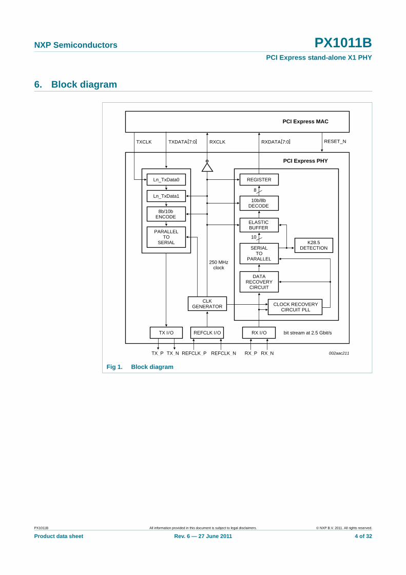
6. Block diagram
Fig 1. Block diagram
8
10
002aac211
Ln_TxData0
TX I/O REFCLK I/O
REFCLK_P
REGISTER
PCI Express PHY
PCI Express MAC
Ln_TxData1
RESET_NRXDATA[7:0]TXDATA[7:0]TXCLK RXCLK
8b/10bENCODE
10b/8bDECODE
REFCLK_NTX_P TX_N
RX I/O
RX_P
bit stream at 2.5 Gbit/s
RX_N
ELASTICBUFFER
K28.5DETECTION
CLOCK RECOVERYCIRCUIT PLL
CLKGENERATOR
250 MHzclock
PARALLELTO
SERIALSERIAL
TOPARALLEL
DATARECOVERY
CIRCUIT
PX1011B All information provided in this document is subject to legal disclaimers. © NXP B.V. 2011. All rights reserved.
Product data sheet Rev. 6 — 27 June 2011 4 of 32
NXP Semiconductors PX1011BPCI Express stand-alone X1 PHY
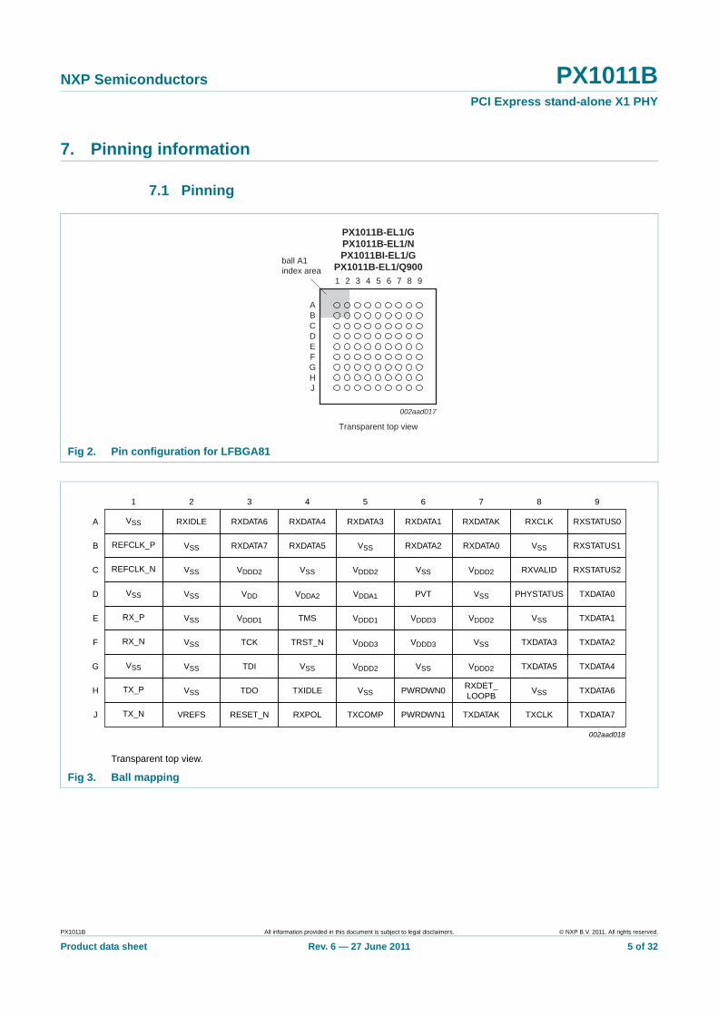
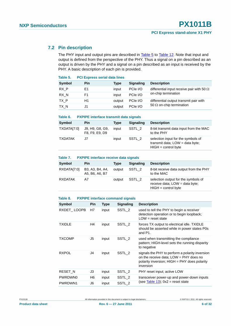
7. Pinning information
7.1 Pinning
Fig 2. Pin configuration for LFBGA81
002aad017
Transparent top view
JHGFED
BC
A
2 4 6 981 3 5 7
ball A1index area
PX1011B-EL1/GPX1011B-EL1/NPX1011BI-EL1/G
PX1011B-EL1/Q900
Transparent top view.
Fig 3. Ball mapping
1
A
002aad018
VSS RXIDLE RXDATA6 RXDATA4 RXDATA3 RXDATA1 RXDATAK RXCLK RXSTATUS0
2 3 4 5 6 7 8 9
B REFCLK_P VSS RXDATA7 RXDATA5 VSS RXDATA2 RXDATA0 VSS RXSTATUS1
C REFCLK_N VSS VDDD2 VSS VDDD2 VSS VDDD2 RXVALID RXSTATUS2
D VSS VSS VDD VDDA2 VDDA1 PVT VSS PHYSTATUS TXDATA0
E RX_P VSS VDDD1 TMS VDDD1 VDDD3 VDDD2 VSS TXDATA1
F RX_N VSS TCK TRST_N VDDD3 VDDD3 VSS TXDATA3 TXDATA2
G VSS VSS TDI VSS VDDD2 VSS VDDD2 TXDATA5 TXDATA4
H TX_P VSS TDO TXIDLE VSS PWRDWN0 RXDET_LOOPB
VSS TXDATA6
J TX_N VREFS RESET_N RXPOL TXCOMP PWRDWN1 TXDATAK TXCLK TXDATA7
PX1011B All information provided in this document is subject to legal disclaimers. © NXP B.V. 2011. All rights reserved.
Product data sheet Rev. 6 — 27 June 2011 5 of 32
NXP Semiconductors PX1011BPCI Express stand-alone X1 PHY
7.2 Pin description
The PHY input and output pins are described in Table 5 to Table 12. Note that input and output is defined from the perspective of the PHY. Thus a signal on a pin described as an output is driven by the PHY and a signal on a pin described as an input is received by the PHY. A basic description of each pin is provided.
Table 5. PCI Express serial data lines
Symbol Pin Type Signaling Description
RX_P E1 input PCIe I/O differential input receive pair with 50 on-chip terminationRX_N F1 input PCIe I/O
TX_P H1 output PCIe I/O differential output transmit pair with 50 on-chip terminationTX_N J1 output PCIe I/O
Table 6. PXPIPE interface transmit data signals
Symbol Pin Type Signaling Description
TXDATA[7:0] J9, H9, G8, G9, F8, F9, E9, D9
input SSTL_2 8-bit transmit data input from the MAC to the PHY
TXDATAK J7 input SSTL_2 selection input for the symbols of transmit data; LOW = data byte; HIGH = control byte
Table 7. PXPIPE interface receive data signals
Symbol Pin Type Signaling Description
RXDATA[7:0] B3, A3, B4, A4, A5, B6, A6, B7
output SSTL_2 8-bit receive data output from the PHY to the MAC
RXDATAK A7 output SSTL_2 selection output for the symbols of receive data; LOW = data byte; HIGH = control byte
Table 8. PXPIPE interface command signals
Symbol Pin Type Signaling Description
RXDET_ LOOPB H7 input SSTL_2 used to tell the PHY to begin a receiver detection operation or to begin loopback; LOW = reset state
TXIDLE H4 input SSTL_2 forces TX output to electrical idle. TXIDLE should be asserted while in power states P0s and P1.
TXCOMP J5 input SSTL_2 used when transmitting the compliance pattern; HIGH-level sets the running disparity to negative
RXPOL J4 input SSTL_2 signals the PHY to perform a polarity inversion on the receive data; LOW = PHY does no polarity inversion; HIGH = PHY does polarity inversion
RESET_N J3 input SSTL_2 PHY reset input; active LOW
PWRDWN0 H6 input SSTL_2 transceiver power-up and power-down inputs (see Table 13); 0x2 = reset statePWRDWN1 J6 input SSTL_2
PX1011B All information provided in this document is subject to legal disclaimers. © NXP B.V. 2011. All rights reserved.
Product data sheet Rev. 6 — 27 June 2011 6 of 32
NXP Semiconductors PX1011BPCI Express stand-alone X1 PHY
Table 9. PXPIPE interface status signals
Symbol Pin Type Signaling Description
RXVALID C8 output SSTL_2 indicates symbol lock and valid data on RX_DATA and RX_DATAK
PHYSTATUS D8 output SSTL_2 used to communicate completion of several PHY functions including power management state transitions and receiver detection
RXIDLE A2 output SSTL_2 indicates receiver detection of an electrical idle; this is an asynchronous signal
RXSTATUS0 A9 output SSTL_2 encodes receiver status and error codes for the received data stream and receiver detection (see Table 15)
RXSTATUS1 B9 output SSTL_2
RXSTATUS2 C9 output SSTL_2
Table 10. Clock and reference signals
Symbol Pin Type Signaling Description
TXCLK J8 input SSTL_2 source synchronous 250 MHz transmit clock input from MAC. All input data and signals to the PHY are synchronized to this clock.
RXCLK A8 output SSTL_2 source synchronous 250 MHz clock output for received data and status signals bound for the MAC.
REFCLK_P B1 input PCIe I/O 100 MHz reference clock input. This is the spread spectrum source clock for PCI Express. Differential pair input with 50 on-chip termination.
REFCLK_N C1 input PCIe I/O
PVT D6 - analog I/O input or output to create a compensation signal internally that will adjust the I/O pads characteristics as PVT drifts. Connect to VDD through a 49.9 resistor.
VREFS J2 input reference voltage input for SSTL_2 class I signaling. Connect to 1.25 V.
Table 11. 3.3 V JTAG signals
Symbol Pin Type Signaling Description
TMS E4 input 3.3 V CMOS test mode select input
TRST_N F4 input 3.3 V CMOS test reset input for the JTAG interface; active LOW
TCK F3 input 3.3 V CMOS test clock input for the JTAG interface
TDI G3 input 3.3 V CMOS test data input
TDO H3 output 3.3 V CMOS test data output
PX1011B All information provided in this document is subject to legal disclaimers. © NXP B.V. 2011. All rights reserved.
Product data sheet Rev. 6 — 27 June 2011 7 of 32
NXP Semiconductors PX1011BPCI Express stand-alone X1 PHY
8. Functional description
The main function of the PHY is to convert digital data into electrical signals and vice versa. The PCI Express PHY handles the low level PCI Express protocol and signaling. The PX1011B PCI Express PHY consists of the Physical Coding Sub-layer (PCS), a Serializer and De-serializer (SerDes) and a set of I/Os (pads). The PCI Express PHY handles the low level PCI Express protocol and signaling. This includes features such as Clock and Data Recovery (CDR), data serialization and de-serialization, 8b/10b encoding, analog buffers, elastic buffer and receiver detection.
The PXPIPE interface between the MAC and PX1011B is a superset of the PHY Interface for the PCI Express (PIPE) specification. The following feature have been added:
• Source synchronous clocks for RX and TX data to simplify timing closure.
The 8-bit data width PXPIPE interface operates at 250 MHz with SSTL_2 class I signaling. PX1011B does not integrate SSTL_2 termination resistors inside the IC.
The PCI Express link consists of a differential input pair and a differential output pair. The data rate of these signals is 2.5 Gbit/s.
8.1 Receiving data
Incoming data enters the chip at the RX interface. The receiver converts these signals from small amplitude differential signals into rail-to-rail digital signals. The carrier detect circuit detects whether data is present on the line and passes this information through to the SerDes and PCS.
If a valid stream of data is present the Clock and Data Recovery unit (CDR) first recovers the clock from the data and then uses this clock for re-timing the data (i.e., recovering the data).
Table 12. PCI Express PHY power supplies
Symbol Pin Type Signaling Description
VDDA1 D5 power 1.2 V analog power supply for serializer and de-serializer
VDDA2 D4 power 3.3 V analog power supply for serializer and de-serializer
VDDD1 E3, E5 power 3.3 V power supply for JTAG I/O
VDDD2 C3, C5, C7, E7, G5, G7
power 2.5 V power supply for SSTL_2 I/O
VDDD3 E6, F5, F6 power 1.2 V power supply for core
VDD D3 power 1.2 V power supply for high-speed serial PCI Express I/O pads and PVT
VSS A1, B2, B5, B8, C2, C4, C6, D1, D2, D7, E2, E8, F2, F7, G1, G2, G4, G6, H2, H5, H8
ground ground
PX1011B All information provided in this document is subject to legal disclaimers. © NXP B.V. 2011. All rights reserved.
Product data sheet Rev. 6 — 27 June 2011 8 of 32
NXP Semiconductors PX1011BPCI Express stand-alone X1 PHY
The de-serializer or Serial-to-Parallel converter (S2P) de-serializes this data into 10-bits parallel data.
Since the S2P has no knowledge about the data, the word alignment is still random. This is fixed in the digital domain by the PCS block. It first detects a 10-bit comma character (K28.5) from the random data stream and aligns the bits. Then it converts the 10-bit raw data into 8-bit words using 8b/10b decoding. An elastic buffer and FIFO brings the resulting data to the right clock domain, which is the RX source synchronous clock domain.
8.2 Transmitting data
When the PHY transmits, it receives 8-bit data from the MAC. This data is encoded using an 8b/10b encoding algorithm. The 2 bits overhead of the 8b/10b encoding ensures the serial data will be DC-balanced and has a sufficient 0-to-1 and 1-to-0 transition density for clock recovery at the receiver side.
The serializer or Parallel-to-Serial converter (P2S) serializes the 10 bits data into serial data streams. These data streams are latched into the transmitter, where they are converted into small amplitude differential signals. The transmitter has built-in de-emphasis for a larger eye opening at the receiver side.
The PLL has a sufficiently high bandwidth to handle a 100 MHz reference clock with a 30 kHz to 33 kHz spread spectrum.
8.3 Clocking
There are three clock signals used by the PX1011B:
• REFCLK is a 100 MHz external reference clock that the PHY uses to generate the 250 MHz data clock and the internal bit rate clock. This clock may have 30 kHz to 33 kHz spread spectrum modulation.
• TXCLK is a reference clock that the PHY uses to clock the TXDATA and command. This source synchronous clock is provided by the MAC. The PHY expects that the rising edge of TXCLK is centered to the data. The TXCLK has to be synchronous with RXCLK.
• RXCLK is a source synchronous clock provided by the PHY. The RXDATA and status signals are synchronous to this clock. The PHY aligns the rising edge of RXCLK to the center of the data. RXCLK may be used by the MAC to clock its internal logic.
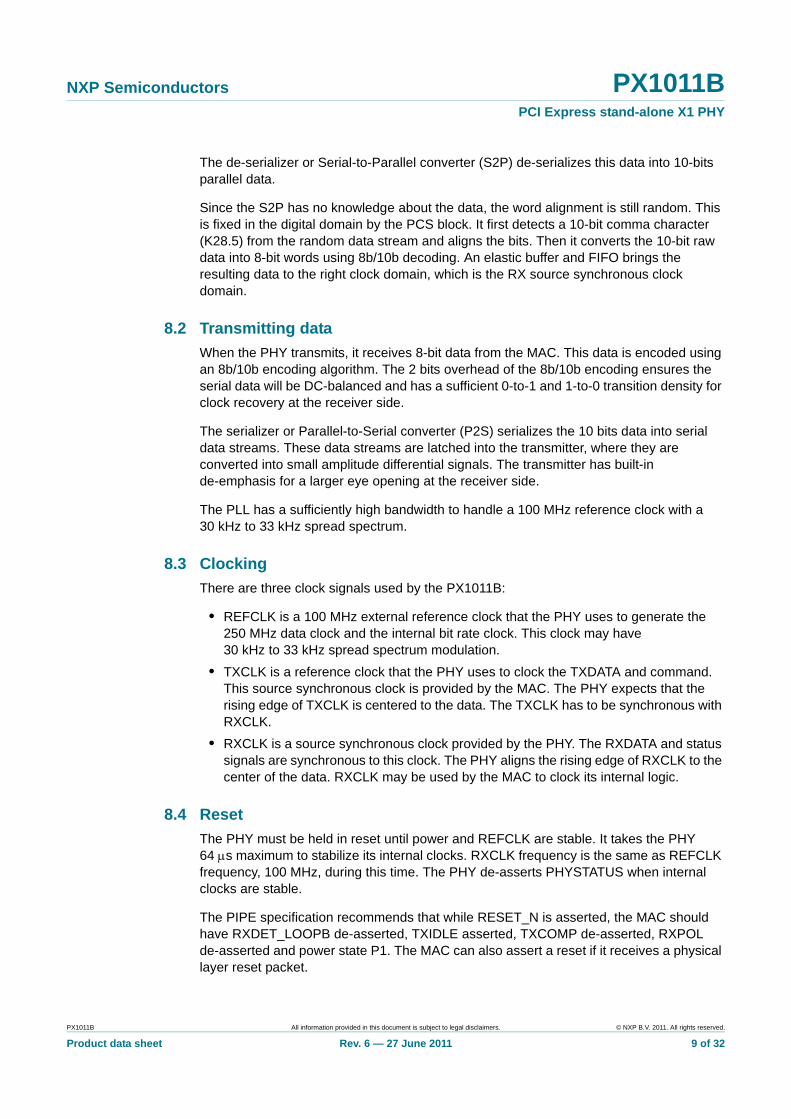
8.4 Reset
The PHY must be held in reset until power and REFCLK are stable. It takes the PHY 64 s maximum to stabilize its internal clocks. RXCLK frequency is the same as REFCLK frequency, 100 MHz, during this time. The PHY de-asserts PHYSTATUS when internal clocks are stable.
The PIPE specification recommends that while RESET_N is asserted, the MAC should have RXDET_LOOPB de-asserted, TXIDLE asserted, TXCOMP de-asserted, RXPOL de-asserted and power state P1. The MAC can also assert a reset if it receives a physical layer reset packet.
PX1011B All information provided in this document is subject to legal disclaimers. © NXP B.V. 2011. All rights reserved.
Product data sheet Rev. 6 — 27 June 2011 9 of 32
NXP Semiconductors PX1011BPCI Express stand-alone X1 PHY
8.5 Power management
The power management signals allow the PHY to manage power consumption. The PHY meets all timing constraints provided in the PCI Express base specification regarding clock recovery and link training for the various power states.
Four power states are defined: P0, P0s, P1 and P2. P0 state is the normal operational state for the PHY. When directed from P0 to a lower power state, the PHY can immediately take whatever power saving measures are appropriate.
In states P0, P0s and P1, the PHY keeps internal clocks operational. For all state transitions between these three states, the PHY indicates successful transition into the designated power state by a single cycle assertion of PHYSTATUS. For all power state transitions, the MAC must not begin any operational sequences or further power state transitions until the PHY has indicated that the initial state transition is completed. TXIDLE should be asserted while in power states P0s and P1.
• P0 state: All internal clocks in the PHY are operational. P0 is the only state where the PHY transmits and receives PCI Express signaling. P0 is the appropriate PHY power management state for most states in the Link Training and Status State Machine (LTSSM). Exceptions are listed for each lower power PHY state (P0s, P1 and P2).
• P0s state: The MAC will move the PHY to this state only when the transmit channel is idle.
While the PHY is in either P0 or P0s power states, if the receiver is detecting an electrical idle, the receiver portion of the PHY can take appropriate power saving measures. Note that the PHY is capable of obtaining bit and symbol lock within the PHY-specified time (N_FTS with or without common clock) upon resumption of signaling on the receive channel. This requirement only applies if the receiver had previously been bit and symbol locked while in P0 or P0s states.
• P1 state: Selected internal clocks in the PHY are turned off. The MAC will move the PHY to this state only when both transmit and receive channels are idle. The PHY indicates a successful entry into P1 (by asserting PHYSTATUS). P1 should be used for the disabled state, all detect states, and L1.idle state of the Link Training and Status State Machine (LTSSM).
• P2 state: PHY will enter P1 instead.
Fig 4. Reset
002aac172
RXCLK
RESET_N
PHYSTATUS
100 MHz 250 MHz
PX1011B All information provided in this document is subject to legal disclaimers. © NXP B.V. 2011. All rights reserved.
Product data sheet Rev. 6 — 27 June 2011 10 of 32
NXP Semiconductors PX1011BPCI Express stand-alone X1 PHY
[1] TXIDLE = 0
[2] TXIDLE = 1
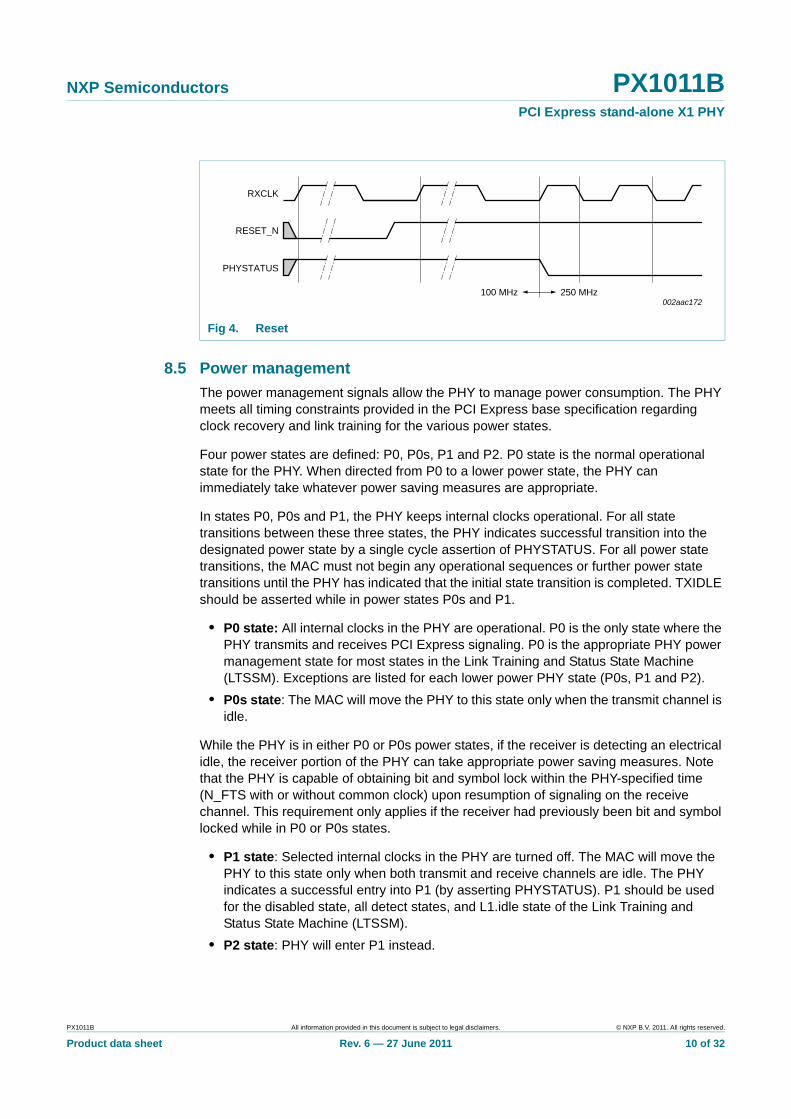
8.6 Receiver detect
When the PHY is in the P1 state, it can be instructed to perform a receiver detection operation to determine if there is a receiver at the other end of the link. Basic operation of receiver detection is that the MAC requests the PHY to do a receiver detect sequence by asserting RXDET_LOOPB. When the PHY has completed the receiver detect sequence, it drives the RXSTATUS signals to the value of 011b if a receiver is present, and to 000b if there is no receiver. Then the PHY will assert PHYSTATUS to indicate the completion of receiver detect operation. The MAC uses the rising edge of PHYSTATUS to sample the RXSTATUS signals and then de-asserts RXDET_LOOPB. A few cycles after the RXDET_LOOPB de-asserts, the PHYSTATUS is also de-asserted.
8.7 Loopback
The PHY supports an internal loopback from the PCI Express receiver to the transmitter with the following characteristics.
The PHY retransmits each 10-bit data and control symbol exactly as received, without applying scrambling or descrambling or disparity corrections, with the following rules:
• If a received 10-bit symbol is determined to be an invalid 10-bit code (i.e., no legal translation to a control or data value possible), the PHY still retransmits the symbol exactly as it was received.
• If a SKP ordered set retransmission requires adding a SKP symbol to accommodate timing tolerance correction, any disparity can be chosen for the SKP symbol.
Table 13. Summary of power management state
PWRDWN[1:0] Power management state Transmitter Receiver TX PLL RXCLK RX PLL/CDR
00b P0, normal operation on[1] on on on on
01b P0s, power saving state idle[2] idle on on on
10b P1, lower power state idle[2] idle on on off
11b illegal, PHY will enter P1 - - - - -
Fig 5. Receiver detect - receiver present
002aac173
RXCLK
000b
10b
011b 000b
PHYSTATUS
RXSTATUS2,RXSTATUS1,RXSTATUS0
TXCLK
RXDET_LOOPB
PWRDWN1,PWRDWN0
PX1011B All information provided in this document is subject to legal disclaimers. © NXP B.V. 2011. All rights reserved.
Product data sheet Rev. 6 — 27 June 2011 11 of 32

NXP Semiconductors PX1011BPCI Express stand-alone X1 PHY
• The PHY continues to provide the received data on the PXPIPE interface, behaving exactly like normal data reception.
• The PHY transitions from normal transmission of data from the PXPIPE interface to looping back the received data at a symbol boundary.
The PHY begins to loopback data when the MAC asserts RXDET_LOOPB while doing normal data transmission. The PHY stops transmitting data from the PXPIPE interface, and begins to loopback received symbols. While doing loopback, the PHY continues to present received data on the PXPIPE interface.
The PHY stops looping back received data when the MAC de-asserts RXDET_LOOPB. Transmission of data on the parallel interface begins immediately.
The timing diagram of Figure 6 shows example timing for beginning loopback. In this example, the receiver is receiving a repeating stream of bytes, Rx-a through Rx-z. Similarly, the MAC is causing the PHY to transmit a repeating stream of bytes Tx-a through Tx-z. When the MAC asserts RXDET_LOOPB to the PHY, the PHY begins to loopback the received data to the differential TX_P and TX_N lines.
The timing diagram of Figure 7 shows an example of switching from loopback mode to normal mode. As soon as the MAC detects an electrical idle ordered-set, the MAC de-asserts RXDET_LOOPB, asserts TXIDLE and changes the POWERDOWN signals to state P1.
Fig 6. Loopback start
RXDET_LOOPB
002aac174
RXCLK
TXCLK
Rx-c Rx-d Rx-e Rx-f Rx-g
Tx-m Tx-n Tx-o Tx-p Tx-q
Tx-m Tx-n Rx-eTX_P, TX_N
RXDATA[7:0]
TXDATA[7:0]
PX1011B All information provided in this document is subject to legal disclaimers. © NXP B.V. 2011. All rights reserved.
Product data sheet Rev. 6 — 27 June 2011 12 of 32

NXP Semiconductors PX1011BPCI Express stand-alone X1 PHY
8.8 Electrical idle
The PCI Express Base Specification requires that devices send an Electrical Idle ordered-set before TX goes to the electrical idle state.
The timing diagram of Figure 8 shows an example of timing for entering electrical idle.
Fig 7. Loopback end
RXDET_LOOPB
001aac785
RXCLK
RXDATA[7:0]
TXIDLE
TX_P, TX_N
TXCLK
COM IDL Junk
Looped back RX data Junk
includes electrical idleordered set
Fig 8. Electrical Idle
TXIDLE
002aac175
TXCLK
TXDATA[7:0]
TXDATAK
ScZero COM IDL
active (ends with Electrical Idle ordered-set)TX_P, TX_N
PX1011B All information provided in this document is subject to legal disclaimers. © NXP B.V. 2011. All rights reserved.
Product data sheet Rev. 6 — 27 June 2011 13 of 32

NXP Semiconductors PX1011BPCI Express stand-alone X1 PHY
Table 14 summarizes the function of some PXPIPE control signals.
8.9 Clock tolerance compensation
The PHY receiver contains an elastic buffer used to compensate for differences in frequencies between bit rates at the two ends of a link. The elastic buffer is capable of holding at least seven symbols to handle worst case differences (600 ppm) in frequency and worst case intervals between SKP ordered-sets. The PHY is responsible for inserting or removing SKP symbols in the received data stream to avoid elastic buffer overflow or underflow. The PHY monitors the receive data stream, and when a Skip ordered-set is received, the PHY can add or remove one SKP symbol from each SKP ordered-set as appropriate to manage its elastic buffer. Whenever a SKP symbol is added or removed, the PHY will signal this to the MAC using the RXSTATUS signals. These signals have a non-zero value for one clock cycle and indicate whether a SKP symbol was added or removed from the received SKP ordered-set. RXSTATUS should be asserted during the clock cycle when the COM symbol of the SKP ordered-set is moved across the parallel interface. If the removal of a SKP symbol causes no SKP symbols to be transferred across the parallel interface, then RXSTATUS is asserted at the same time that the COM symbol (that was part of the received skip ordered-set) is transmitted across the parallel interface.
Figure 9 shows a sequence where the PHY inserted a SKP symbol in the data stream.
Figure 10 shows a sequence where the PHY removed a SKP symbol from a SKP ordered-set.
Table 14. Control signals function summary
PWRDWN[1:0] RXDET_LOOPB TXIDLE Function description
P0: 00b 0 0 normal operation
0 1 transmitter in idle
1 0 loopback mode
1 1 illegal
P0s: 01b X 0 illegal
1 transmitter in idle
P1: 10b X 0 illegal
0 1 transmitter in idle
1 1 receiver detect
Fig 9. Clock correction - insert a SKP
001aac779
RXCLK
active COM SKP
000b 001b 000b
SKP active
RXVALID
RXDATA[7:0]
RXSTATUS2,RXSTATUS1,RXSTATUS0
PX1011B All information provided in this document is subject to legal disclaimers. © NXP B.V. 2011. All rights reserved.
Product data sheet Rev. 6 — 27 June 2011 14 of 32
NXP Semiconductors PX1011BPCI Express stand-alone X1 PHY
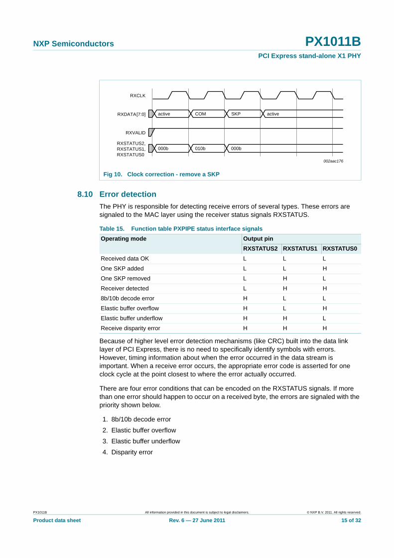
8.10 Error detection
The PHY is responsible for detecting receive errors of several types. These errors are signaled to the MAC layer using the receiver status signals RXSTATUS.
Because of higher level error detection mechanisms (like CRC) built into the data link layer of PCI Express, there is no need to specifically identify symbols with errors. However, timing information about when the error occurred in the data stream is important. When a receive error occurs, the appropriate error code is asserted for one clock cycle at the point closest to where the error actually occurred.
There are four error conditions that can be encoded on the RXSTATUS signals. If more than one error should happen to occur on a received byte, the errors are signaled with the priority shown below.
1. 8b/10b decode error
2. Elastic buffer overflow
3. Elastic buffer underflow
4. Disparity error
Fig 10. Clock correction - remove a SKP
002aac176
RXCLK
active COM SKP
000b 010b 000b
active
RXVALID
RXDATA[7:0]
RXSTATUS2,RXSTATUS1,RXSTATUS0
Table 15. Function table PXPIPE status interface signals
Operating mode Output pin
RXSTATUS2 RXSTATUS1 RXSTATUS0
Received data OK L L L
One SKP added L L H
One SKP removed L H L
Receiver detected L H H
8b/10b decode error H L L
Elastic buffer overflow H L H
Elastic buffer underflow H H L
Receive disparity error H H H
PX1011B All information provided in this document is subject to legal disclaimers. © NXP B.V. 2011. All rights reserved.
Product data sheet Rev. 6 — 27 June 2011 15 of 32
NXP Semiconductors PX1011BPCI Express stand-alone X1 PHY
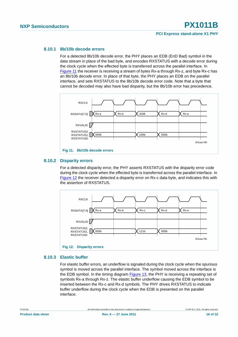
8.10.1 8b/10b decode errors
For a detected 8b/10b decode error, the PHY places an EDB (EnD Bad) symbol in the data stream in place of the bad byte, and encodes RXSTATUS with a decode error during the clock cycle when the effected byte is transferred across the parallel interface. In Figure 11 the receiver is receiving a stream of bytes Rx-a through Rx-z, and byte Rx-c has an 8b/10b decode error. In place of that byte, the PHY places an EDB on the parallel interface, and sets RXSTATUS to the 8b/10b decode error code. Note that a byte that cannot be decoded may also have bad disparity, but the 8b/10b error has precedence.
8.10.2 Disparity errors
For a detected disparity error, the PHY asserts RXSTATUS with the disparity error code during the clock cycle when the effected byte is transferred across the parallel interface. In Figure 12 the receiver detected a disparity error on Rx-c data byte, and indicates this with the assertion of RXSTATUS.
8.10.3 Elastic buffer
For elastic buffer errors, an underflow is signaled during the clock cycle when the spurious symbol is moved across the parallel interface. The symbol moved across the interface is the EDB symbol. In the timing diagram Figure 13, the PHY is receiving a repeating set of symbols Rx-a through Rx-z. The elastic buffer underflow causing the EDB symbol to be inserted between the Rx-c and Rx-d symbols. The PHY drives RXSTATUS to indicate buffer underflow during the clock cycle when the EDB is presented on the parallel interface.
Fig 11. 8b/10b decode errors
001aac780
RXCLK
Rx-a Rx-b EDB
000b 100b 000b
Rx-d Rx-e
RXVALID
RXDATA[7:0]
RXSTATUS2,RXSTATUS1,RXSTATUS0
Fig 12. Disparity errors
001aac781
RXCLK
Rx-a Rx-b Rx-c
000b 111b 000b
Rx-d Rx-e
RXVALID
RXDATA[7:0]
RXSTATUS2,RXSTATUS1,RXSTATUS0
PX1011B All information provided in this document is subject to legal disclaimers. © NXP B.V. 2011. All rights reserved.
Product data sheet Rev. 6 — 27 June 2011 16 of 32
NXP Semiconductors PX1011BPCI Express stand-alone X1 PHY
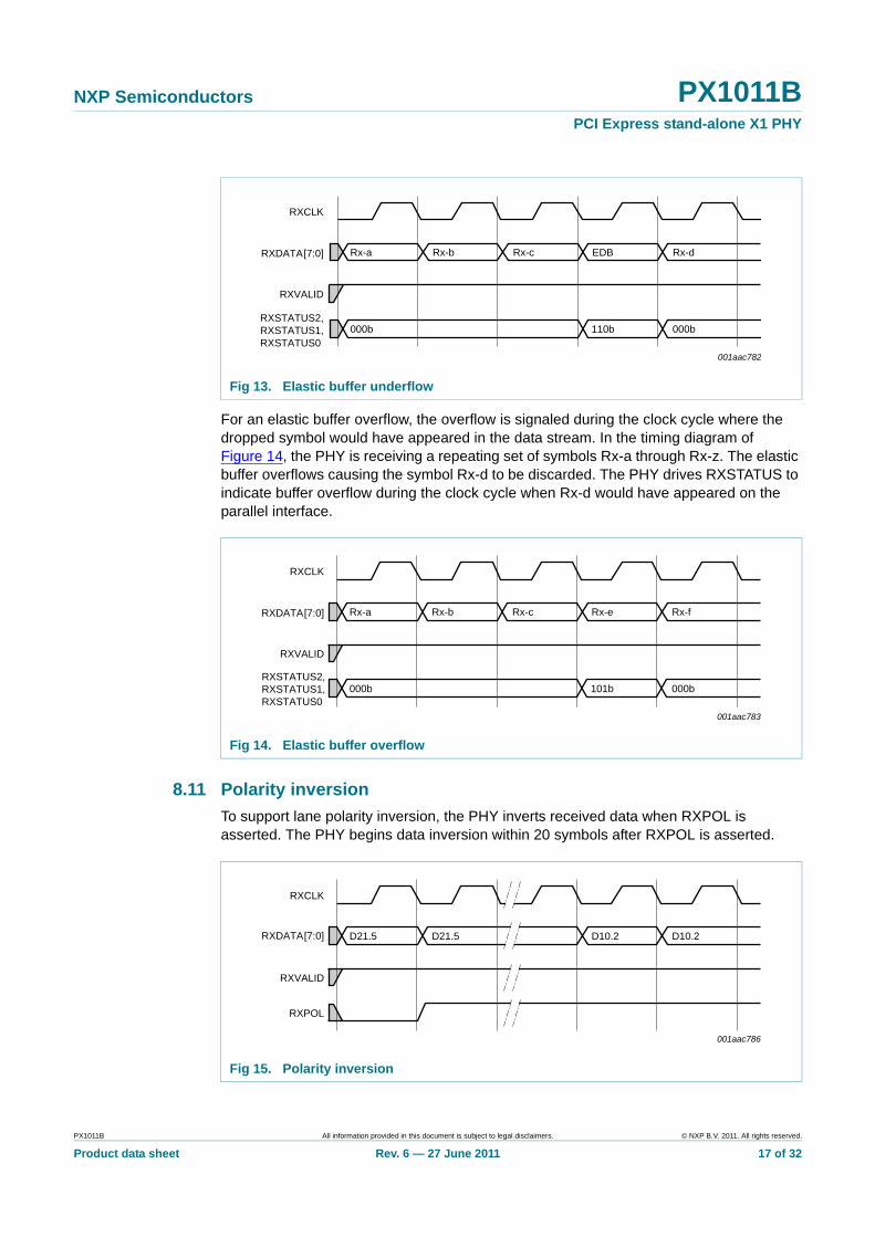
For an elastic buffer overflow, the overflow is signaled during the clock cycle where the dropped symbol would have appeared in the data stream. In the timing diagram of Figure 14, the PHY is receiving a repeating set of symbols Rx-a through Rx-z. The elastic buffer overflows causing the symbol Rx-d to be discarded. The PHY drives RXSTATUS to indicate buffer overflow during the clock cycle when Rx-d would have appeared on the parallel interface.
8.11 Polarity inversion
To support lane polarity inversion, the PHY inverts received data when RXPOL is asserted. The PHY begins data inversion within 20 symbols after RXPOL is asserted.
Fig 13. Elastic buffer underflow
Fig 14. Elastic buffer overflow
001aac782
RXCLK
Rx-a Rx-b Rx-c
000b 110b 000b
EDB Rx-d
RXVALID
RXDATA[7:0]
RXSTATUS2,RXSTATUS1,RXSTATUS0
001aac783
RXCLK
Rx-a Rx-b Rx-c
000b 101b 000b
Rx-e Rx-f
RXVALID
RXDATA[7:0]
RXSTATUS2,RXSTATUS1,RXSTATUS0
Fig 15. Polarity inversion
001aac786
RXCLK
D21.5 D21.5 D10.2 D10.2
RXPOL
RXVALID
RXDATA[7:0]
PX1011B All information provided in this document is subject to legal disclaimers. © NXP B.V. 2011. All rights reserved.
Product data sheet Rev. 6 — 27 June 2011 17 of 32
NXP Semiconductors PX1011BPCI Express stand-alone X1 PHY
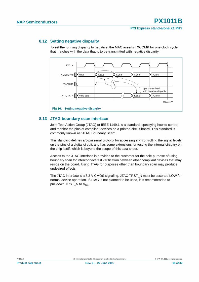
8.12 Setting negative disparity
To set the running disparity to negative, the MAC asserts TXCOMP for one clock cycle that matches with the data that is to be transmitted with negative disparity.
8.13 JTAG boundary scan interface
Joint Test Action Group (JTAG) or IEEE 1149.1 is a standard, specifying how to control and monitor the pins of compliant devices on a printed-circuit board. This standard is commonly known as ‘JTAG Boundary Scan’.
This standard defines a 5-pin serial protocol for accessing and controlling the signal levels on the pins of a digital circuit, and has some extensions for testing the internal circuitry on the chip itself, which is beyond the scope of this data sheet.
Access to the JTAG interface is provided to the customer for the sole purpose of using boundary scan for interconnect test verification between other compliant devices that may reside on the board. Using JTAG for purposes other than boundary scan may produce undesired effects.
The JTAG interface is a 3.3 V CMOS signaling. JTAG TRST_N must be asserted LOW for normal device operation. If JTAG is not planned to be used, it is recommended to pull down TRST_N to VSS.
Fig 16. Setting negative disparity
002aac177
TXCLK
data K28.5 K28.5
valid data K28.5− K28.5+
K28.5 K28.5
TX_P, TX_N
TXCOMP
TXDATA[7:0]
byte transmittedwith negative disparity
PX1011B All information provided in this document is subject to legal disclaimers. © NXP B.V. 2011. All rights reserved.
Product data sheet Rev. 6 — 27 June 2011 18 of 32
NXP Semiconductors PX1011BPCI Express stand-alone X1 PHY
9. Limiting values
[1] Human Body Model: ANSI/EOS/ESD-S5.1-1994, standard for ESD sensitivity testing, Human Body Model - Component level; Electrostatic Discharge Association, Rome, NY, USA.
[2] Charged Device Model: ANSI/EOS/ESD-S5.3.1-1999, standard for ESD sensitivity testing, Charged Device Model - component level; Electrostatic Discharge Association, Rome, NY, USA.
10. Thermal characteristics
[1] Significant variations can be expected due to system variables, such as adjacent devices, or actual air flow across the package.
Table 16. Limiting valuesIn accordance with the Absolute Maximum Rating System (IEC 60134).
Symbol Parameter Conditions Min Max Unit
VDDD1 digital supply voltage 1 for JTAG I/O 0.5 +4.6 V
VDDD2 digital supply voltage 2 for SSTL_2 I/O 0.5 +3.75 V
VDDD3 digital supply voltage 3 for core 0.5 +1.7 V
VDD supply voltage for high-speed serial I/O and PVT
0.5 +1.7 V
VDDA1 analog supply voltage 1 for serializer 0.5 +1.7 V
VDDA2 analog supply voltage 2 for serializer 0.5 +4.6 V
VESD electrostatic discharge voltage HBM [1] - 2000 V
CDM [2] - 500 V
Tstg storage temperature 55 +150 C
Tj junction temperature 55 +125 C
Tamb ambient temperature operating
commercial 0 +70 C
industrial 40 +85 C
Table 17. Thermal characteristics
Symbol Parameter Conditions Typ Unit
Rth(j-a) thermal resistance from junction to ambient in free air [1] 44 K/W
Rth(j-c) thermal resistance from junction to case in free air [1] 10 K/W
PX1011B All information provided in this document is subject to legal disclaimers. © NXP B.V. 2011. All rights reserved.
Product data sheet Rev. 6 — 27 June 2011 19 of 32
NXP Semiconductors PX1011BPCI Express stand-alone X1 PHY
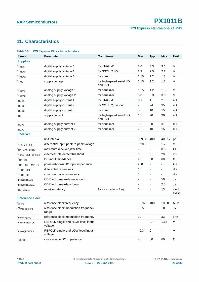
11. Characteristics
Table 18. PCI Express PHY characteristics
Symbol Parameter Conditions Min Typ Max Unit
Supplies
VDDD1 digital supply voltage 1 for JTAG I/O 3.0 3.3 3.6 V
VDDD2 digital supply voltage 2 for SSTL_2 I/O 2.3 2.5 2.7 V
VDDD3 digital supply voltage 3 for core 1.15 1.2 1.3 V
VDD supply voltage for high-speed serial I/O and PVT
1.15 1.2 1.3 V
VDDA1 analog supply voltage 1 for serializer 1.15 1.2 1.3 V
VDDA2 analog supply voltage 2 for serializer 3.0 3.3 3.6 V
IDDD1 digital supply current 1 for JTAG I/O 0.1 1 2 mA
IDDD2 digital supply current 2 for SSTL_2; no load - 24 35 mA
IDDD3 digital supply current 3 for core 5 10 15 mA
IDD supply current for high-speed serial I/O and PVT
15 20 30 mA
IDDA1 analog supply current 1 for serializer 15 20 31 mA
IDDA2 analog supply current 2 for serializer 7 10 15 mA
Receiver
UI unit interval 399.88 400 400.12 ps
VRX_DIFFp-p differential input peak-to-peak voltage 0.205 - 1.2 V
tRX_MAX_JITTER maximum receiver jitter time - - 0.6 UI
VIDLE_DET_DIFFp-p electrical idle detect threshold 65 - 205 mV
ZRX_DC DC input impedance 40 50 60
ZRX_HIGH_IMP_DC powered-down DC input impedance 200 - - k
RLRX_DIFF differential return loss 15 - - dB
RLRX_CM common mode return loss 6 - - dB
tlock(CDR)(ref) CDR lock time (reference loop) - - 50 s
tlock(CDR)(data) CDR lock time (data loop) - - 2.5 s
tRX_latency receiver latency 1 clock cycle is 4 ns 6 - 13 clock cycle
Reference clock
fclk(ref) reference clock frequency 99.97 100 100.03 MHz
fmod(clk)(ref) reference clock modulation frequency range
0.5 - +0 %
fmod(clk)(ref) reference clock modulation frequency 30 - 33 kHz
VIH(se)REFCLK REFCLK single-end HIGH-level input voltage
- 0.7 1.15 V
VIL(se)REFCLK REFCLK single-end LOW-level input voltage
0.3 0 - V
ZC-DC clock source DC impedance 40 50 60
PX1011B All information provided in this document is subject to legal disclaimers. © NXP B.V. 2011. All rights reserved.
Product data sheet Rev. 6 — 27 June 2011 20 of 32
NXP Semiconductors PX1011BPCI Express stand-alone X1 PHY
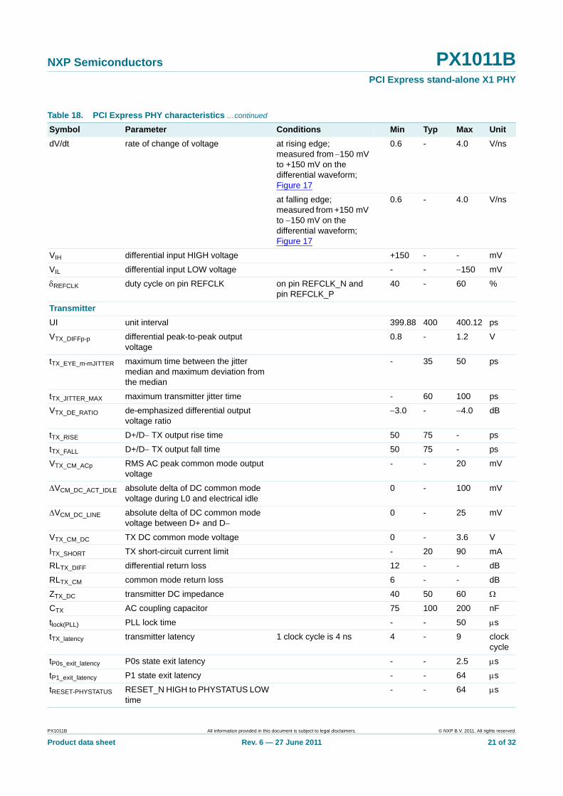
dV/dt rate of change of voltage at rising edge; measured from 150 mV to +150 mV on the differential waveform; Figure 17
0.6 - 4.0 V/ns
at falling edge; measured from +150 mV to 150 mV on the differential waveform; Figure 17
0.6 - 4.0 V/ns
VIH differential input HIGH voltage +150 - - mV
VIL differential input LOW voltage - - 150 mV
REFCLK duty cycle on pin REFCLK on pin REFCLK_N and pin REFCLK_P
40 - 60 %
Transmitter
UI unit interval 399.88 400 400.12 ps
VTX_DIFFp-p differential peak-to-peak output voltage
0.8 - 1.2 V
tTX_EYE_m-mJITTER maximum time between the jitter median and maximum deviation from the median
- 35 50 ps
tTX_JITTER_MAX maximum transmitter jitter time - 60 100 ps
VTX_DE_RATIO de-emphasized differential output voltage ratio
3.0 - 4.0 dB
tTX_RISE D+/D TX output rise time 50 75 - ps
tTX_FALL D+/D TX output fall time 50 75 - ps
VTX_CM_ACp RMS AC peak common mode output voltage
- - 20 mV
VCM_DC_ACT_IDLE absolute delta of DC common mode voltage during L0 and electrical idle
0 - 100 mV
VCM_DC_LINE absolute delta of DC common mode voltage between D+ and D
0 - 25 mV
VTX_CM_DC TX DC common mode voltage 0 - 3.6 V
ITX_SHORT TX short-circuit current limit - 20 90 mA
RLTX_DIFF differential return loss 12 - - dB
RLTX_CM common mode return loss 6 - - dB
ZTX_DC transmitter DC impedance 40 50 60
CTX AC coupling capacitor 75 100 200 nF
tlock(PLL) PLL lock time - - 50 s
tTX_latency transmitter latency 1 clock cycle is 4 ns 4 - 9 clock cycle
tP0s_exit_latency P0s state exit latency - - 2.5 s
tP1_exit_latency P1 state exit latency - - 64 s
tRESET-PHYSTATUS RESET_N HIGH to PHYSTATUS LOW time
- - 64 s
Table 18. PCI Express PHY characteristics …continued
Symbol Parameter Conditions Min Typ Max Unit
PX1011B All information provided in this document is subject to legal disclaimers. © NXP B.V. 2011. All rights reserved.
Product data sheet Rev. 6 — 27 June 2011 21 of 32

NXP Semiconductors PX1011BPCI Express stand-alone X1 PHY
[1] Reference voltage for SSTL_2 class I I/O.
Fig 17. Differential measurement points
dV/dtat rising edge
dV/dtat falling edge
002aad694
VIH = +150 mV
0.0 V
VIL = −150 mV
REFCLK+minus
REFCLK−
Table 19. PXPIPE characteristics
Symbol Parameter Conditions Min Typ Max Unit
fRXCLK RXCLK frequency 249.925 250 250.075 MHz
fTXCLK TXCLK frequency 249.925 250 250.075 MHz
VVREFS voltage on pin VREFS [1] 1.13 1.25 1.38 V
VOH(SSTL2) SSTL_2 HIGH-level output voltage AC VTT + 0.61 - - V
VOL(SSTL2) SSTL_2 LOW-level output voltage AC - - VTT 0.61 V
VIH(SSTL2) SSTL_2 HIGH-level input voltage AC Vref + 0.31 - - V
VIL(SSTL2) SSTL_2 LOW-level input voltage AC - - Vref 0.31 V
Input signals; measured with respect to TXCLK
tsu(TX)(PXPIPE) set-up time of PXPIPE input signal see Figure 18 500 - - ps
th(TX)(PXPIPE) hold time of PXPIPE input signal see Figure 18 500 - - ps
Output signals; measured with respect to RXCLK
tsu(RX)(PXPIPE) set-up time of PXPIPE output signal see Figure 18 1500 - - ps
th(RX)(PXPIPE) hold time of PXPIPE output signal see Figure 18 1500 - - ps
Fig 18. Definition of PXPIPE timing
PXPIPEINPUT
TXCLK
PXPIPEOUTPUT
RXCLK
th(RX)(PXPIPE)tsu(RX)(PXPIPE)
th(TX)(PXPIPE)tsu(TX)(PXPIPE)
002aac316
PX1011B All information provided in this document is subject to legal disclaimers. © NXP B.V. 2011. All rights reserved.
Product data sheet Rev. 6 — 27 June 2011 22 of 32
NXP Semiconductors PX1011BPCI Express stand-alone X1 PHY
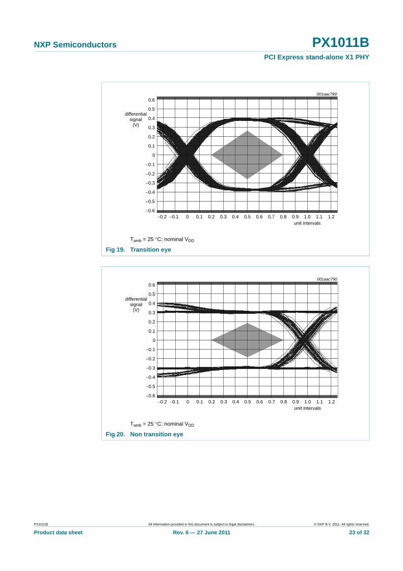
Tamb = 25 C; nominal VDD
Fig 19. Transition eye
Tamb = 25 C; nominal VDD
Fig 20. Non transition eye
−0.2−0.6
−0.5
−0.4
−0.3
−0.2
−0.1
0
0.1
0.2
0.3
0.4
0.5
0.6
−0.1 0
differentialsignal
(V)
0.1 0.2 0.3 0.4 0.5 0.6 0.7 0.8 0.9 1.0unit intervals
1.1 1.2
001aac789
−0.2−0.6
−0.5
−0.4
−0.3
−0.2
−0.1
0
0.1
0.2
0.3
0.4
0.5
0.6
−0.1 0
differentialsignal
(V)
0.1 0.2 0.3 0.4 0.5 0.6 0.7 0.8 0.9 1.0unit intervals
1.1 1.2
001aac790
PX1011B All information provided in this document is subject to legal disclaimers. © NXP B.V. 2011. All rights reserved.
Product data sheet Rev. 6 — 27 June 2011 23 of 32
NXP Semiconductors PX1011BPCI Express stand-alone X1 PHY
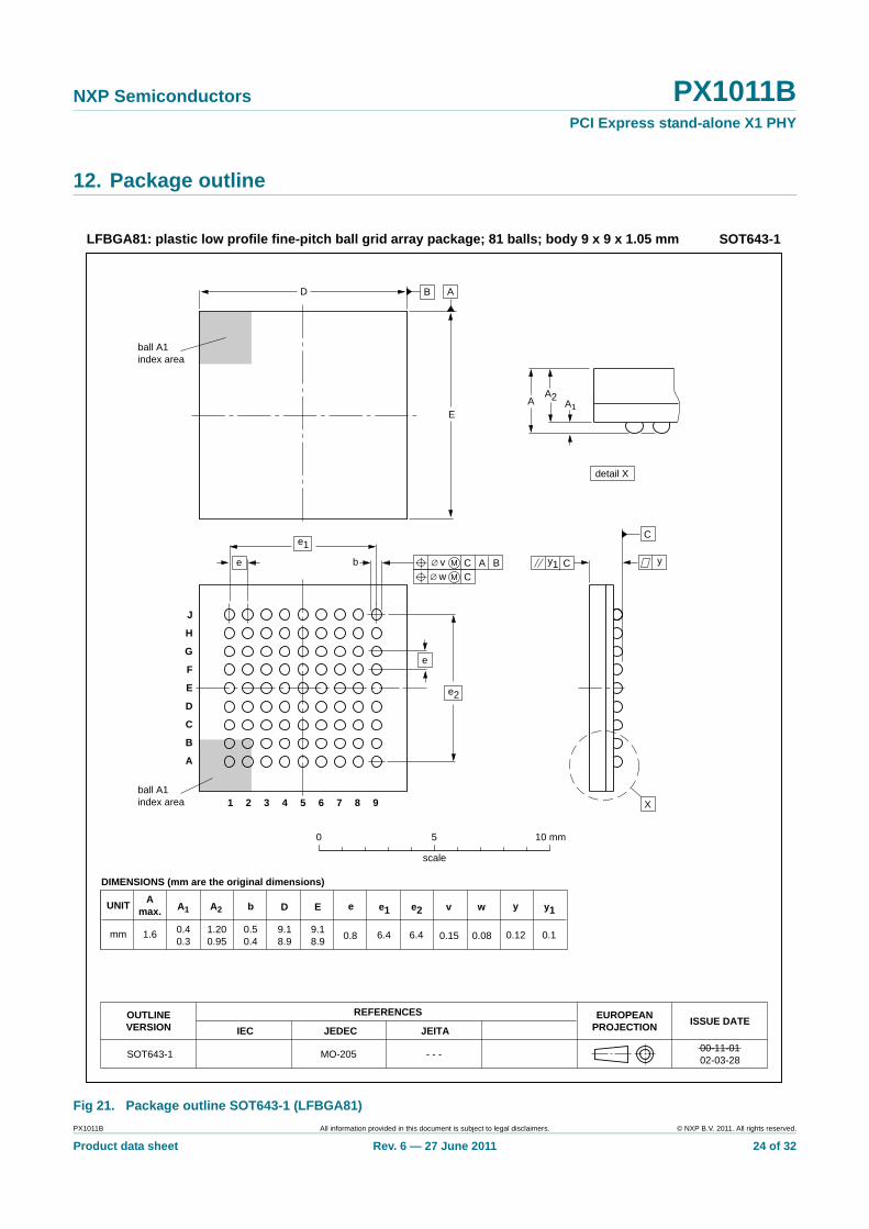
12. Package outline
Fig 21. Package outline SOT643-1 (LFBGA81)
ball A1index area
0.8
A1 bA2UNIT D ye
REFERENCESOUTLINEVERSION
EUROPEANPROJECTION ISSUE DATE
00-11-0102-03-28
IEC JEDEC JEITA
mm 1.6 0.40.3
1.200.95
9.18.9
y1
9.18.9
0.50.4
0.12 0.1
e1
6.4
e2
6.4
DIMENSIONS (mm are the original dimensions)
SOT643-1 MO-205 - - -
E
0.15
v
0.08
w
0 5 10 mm
scale
SOT643-1LFBGA81: plastic low profile fine-pitch ball grid array package; 81 balls; body 9 x 9 x 1.05 mm
Amax.
AA2
A1
detail X
yy1 C
X
D
E
C
A
B
C
D
E
F
H
G
J
2 4 6 981 3 5 7
B A
ball A1index area
e
e
e1
b
e2
ACC
B∅ v M
∅ w M
PX1011B All information provided in this document is subject to legal disclaimers. © NXP B.V. 2011. All rights reserved.
Product data sheet Rev. 6 — 27 June 2011 24 of 32

NXP Semiconductors PX1011BPCI Express stand-alone X1 PHY
13. Soldering of SMD packages
This text provides a very brief insight into a complex technology. A more in-depth account of soldering ICs can be found in Application Note AN10365 “Surface mount reflow soldering description”.
13.1 Introduction to soldering
Soldering is one of the most common methods through which packages are attached to Printed Circuit Boards (PCBs), to form electrical circuits. The soldered joint provides both the mechanical and the electrical connection. There is no single soldering method that is ideal for all IC packages. Wave soldering is often preferred when through-hole and Surface Mount Devices (SMDs) are mixed on one printed wiring board; however, it is not suitable for fine pitch SMDs. Reflow soldering is ideal for the small pitches and high densities that come with increased miniaturization.
13.2 Wave and reflow soldering
Wave soldering is a joining technology in which the joints are made by solder coming from a standing wave of liquid solder. The wave soldering process is suitable for the following:
• Through-hole components
• Leaded or leadless SMDs, which are glued to the surface of the printed circuit board
Not all SMDs can be wave soldered. Packages with solder balls, and some leadless packages which have solder lands underneath the body, cannot be wave soldered. Also, leaded SMDs with leads having a pitch smaller than ~0.6 mm cannot be wave soldered, due to an increased probability of bridging.
The reflow soldering process involves applying solder paste to a board, followed by component placement and exposure to a temperature profile. Leaded packages, packages with solder balls, and leadless packages are all reflow solderable.
Key characteristics in both wave and reflow soldering are:
• Board specifications, including the board finish, solder masks and vias
• Package footprints, including solder thieves and orientation
• The moisture sensitivity level of the packages
• Package placement
• Inspection and repair
• Lead-free soldering versus SnPb soldering
13.3 Wave soldering
Key characteristics in wave soldering are:
• Process issues, such as application of adhesive and flux, clinching of leads, board transport, the solder wave parameters, and the time during which components are exposed to the wave
• Solder bath specifications, including temperature and impurities
PX1011B All information provided in this document is subject to legal disclaimers. © NXP B.V. 2011. All rights reserved.
Product data sheet Rev. 6 — 27 June 2011 25 of 32
NXP Semiconductors PX1011BPCI Express stand-alone X1 PHY
13.4 Reflow soldering
Key characteristics in reflow soldering are:
• Lead-free versus SnPb soldering; note that a lead-free reflow process usually leads to higher minimum peak temperatures (see Figure 22) than a SnPb process, thus reducing the process window
• Solder paste printing issues including smearing, release, and adjusting the process window for a mix of large and small components on one board
• Reflow temperature profile; this profile includes preheat, reflow (in which the board is heated to the peak temperature) and cooling down. It is imperative that the peak temperature is high enough for the solder to make reliable solder joints (a solder paste characteristic). In addition, the peak temperature must be low enough that the packages and/or boards are not damaged. The peak temperature of the package depends on package thickness and volume and is classified in accordance with Table 20 and 21
Moisture sensitivity precautions, as indicated on the packing, must be respected at all times.
Studies have shown that small packages reach higher temperatures during reflow soldering, see Figure 22.
Table 20. SnPb eutectic process (from J-STD-020C)
Package thickness (mm) Package reflow temperature (C)
Volume (mm3)
< 350 350
< 2.5 235 220
2.5 220 220
Table 21. Lead-free process (from J-STD-020C)
Package thickness (mm) Package reflow temperature (C)
Volume (mm3)
< 350 350 to 2000 > 2000
< 1.6 260 260 260
1.6 to 2.5 260 250 245
> 2.5 250 245 245
PX1011B All information provided in this document is subject to legal disclaimers. © NXP B.V. 2011. All rights reserved.
Product data sheet Rev. 6 — 27 June 2011 26 of 32
NXP Semiconductors PX1011BPCI Express stand-alone X1 PHY
For further information on temperature profiles, refer to Application Note AN10365 “Surface mount reflow soldering description”.
14. Appendix
14.1 Errata added 2009-09-01
The PX1011B (types PX1011B-EL1/G, PX1011BI-EL1/G, PX1011B-EL1/N and PX1011B-EL1/Q900) is reported to sporadically produce communication failures in Intel DX58S0-based systems in which the PCIe transmitter has full Active Power State Management (ASPM) capability, and particularly when L0s mode is supported.
When the PCIe transmitter goes idle (enters L0s) for the purpose of power saving and then returns to normal mode (exits L0s and enters L0), the PX1011B receiver PLL may randomly fail to lock, preventing it from properly interpreting the data being transmitted on the link. As a result the PX1011B may send symbols to the link device that it cannot recognize.
This is a L0s exit failure which may prevent the system from recovering and could cause the PCIe protocol to eventually fail and the link to go down. If this occurs, the PX1011B stays in the exit failure state indefinitely. The receiver can only be re-initiated by applying a hard reset to the PHY, returning it to normal mode.
You are strongly advised to disable the L0s mode whenever the PX1011B is used.
MSL: Moisture Sensitivity Level
Fig 22. Temperature profiles for large and small components
001aac844
temperature
time
minimum peak temperature= minimum soldering temperature
maximum peak temperature= MSL limit, damage level
peak temperature
PX1011B All information provided in this document is subject to legal disclaimers. © NXP B.V. 2011. All rights reserved.
Product data sheet Rev. 6 — 27 June 2011 27 of 32
NXP Semiconductors PX1011BPCI Express stand-alone X1 PHY
15. Abbreviations
16. References
[1] PCI Express Base Specification — Rev. 1.0a - PCISIG
[2] PHY Interface for the PCI Express Architecture (PIPE) Specification Version 1.00 — Intel Corporation
Table 22. Abbreviations
Acronym Description
BER Bit Error Rate
BIST Built-In Self Test
CMOS Complementary Metal-Oxide Semiconductor
CRC Cyclic Redundancy Check
EMI ElectroMagnetic Interference
ESD ElectroStatic Discharge
FPGA Field Programmable Gate Array
LTSSM Link Training and Status State Machine
MAC Media Access Control
P2S Parallel to Serial
PCI Peripheral Component Interconnect
PCS Physical Coding Sub-layer
PHY PHYsical layer
PLL Phase-Locked Loop
PIPE PHY Interface for the PCI Express
PVT Process Voltage Temperature
S2P Serial to Parallel
SerDes Serializer and De-serializer
SKP SKiP
SSTL_2 Stub Series Terminated Logic for 2.5 Volts
PX1011B All information provided in this document is subject to legal disclaimers. © NXP B.V. 2011. All rights reserved.
Product data sheet Rev. 6 — 27 June 2011 28 of 32
NXP Semiconductors PX1011BPCI Express stand-alone X1 PHY
17. Revision history
Table 23. Revision history
Document ID Release date Data sheet status Change notice Supersedes
PX1011B v.6 20110627 Product data sheet - PX1011B v.5
Modifications: • Section 1 “General description”, third paragraph: added last sentence
PX1011B v.5 20110418 Product data sheet - PX1011B v.4
Modifications: • Table 2 “Ordering information”:
– Added type number PX1011B-EL1/Q900
– Added Table note [1] and cross-reference at PX1011B-EL1/Q900
• Table 4 “Lead-free package marking”: added marking PX1011B-EL1/Q
• Figure 2 “Pin configuration for LFBGA81”: added type number PX1011B-EL1/Q900
• Table 18 “PCI Express PHY characteristics”:
– sub-section “Supplies”, IDD, supply current: Max value changed from “28 mA” to “30 mA”
– sub-section “Supplies”, IDDA1, analog supply current 1: Max value changed from “28 mA” to “31 mA”
– sub-section “Receiver”, VRX_DIFFp-p, differential input peak-to-peak voltage: Min value changed from “0.175 V” to “0.205 V”
– sub-section “Receiver”, VIDLE_DET_DIFFp-p, electrical idle detect threshold: Max value changed from “175 mV” to “205 mV”
• Section 14.1 “Errata added 2009-09-01”: added type number PX1011B-EL1/Q900 to first sentence
PX1011B v.4 20090904 Product data sheet - PX1011B v.3
Modifications: • Section 14: Errata information added
PX1011B v.3 20081020 Product data sheet - PX1011B v.2
Modifications: • Added type number PX1011B-EL1/N (affects Section 2.6 “Miscellaneous”, Table 2 “Ordering information”, (new) Table 3 “Leaded package marking”, Figure 2 “Pin configuration for LFBGA81”)
PX1011B v.2 20080319 Product data sheet - PX1011B v.1
PX1011B v.1 20080213 Objective data sheet - -
PX1011B All information provided in this document is subject to legal disclaimers. © NXP B.V. 2011. All rights reserved.
Product data sheet Rev. 6 — 27 June 2011 29 of 32
NXP Semiconductors PX1011BPCI Express stand-alone X1 PHY
18. Legal information
18.1 Data sheet status
[1] Please consult the most recently issued document before initiating or completing a design.
[2] The term ‘short data sheet’ is explained in section “Definitions”.
[3] The product status of device(s) described in this document may have changed since this document was published and may differ in case of multiple devices. The latest product status information is available on the Internet at URL http://www.nxp.com.
18.2 Definitions
Draft — The document is a draft version only. The content is still under internal review and subject to formal approval, which may result in modifications or additions. NXP Semiconductors does not give any representations or warranties as to the accuracy or completeness of information included herein and shall have no liability for the consequences of use of such information.
Short data sheet — A short data sheet is an extract from a full data sheet with the same product type number(s) and title. A short data sheet is intended for quick reference only and should not be relied upon to contain detailed and full information. For detailed and full information see the relevant full data sheet, which is available on request via the local NXP Semiconductors sales office. In case of any inconsistency or conflict with the short data sheet, the full data sheet shall prevail.
Product specification — The information and data provided in a Product data sheet shall define the specification of the product as agreed between NXP Semiconductors and its customer, unless NXP Semiconductors and customer have explicitly agreed otherwise in writing. In no event however, shall an agreement be valid in which the NXP Semiconductors product is deemed to offer functions and qualities beyond those described in the Product data sheet.
18.3 Disclaimers
Limited warranty and liability — Information in this document is believed to be accurate and reliable. However, NXP Semiconductors does not give any representations or warranties, expressed or implied, as to the accuracy or completeness of such information and shall have no liability for the consequences of use of such information.
In no event shall NXP Semiconductors be liable for any indirect, incidental, punitive, special or consequential damages (including - without limitation - lost profits, lost savings, business interruption, costs related to the removal or replacement of any products or rework charges) whether or not such damages are based on tort (including negligence), warranty, breach of contract or any other legal theory.
Notwithstanding any damages that customer might incur for any reason whatsoever, NXP Semiconductors’ aggregate and cumulative liability towards customer for the products described herein shall be limited in accordance with the Terms and conditions of commercial sale of NXP Semiconductors.
Right to make changes — NXP Semiconductors reserves the right to make changes to information published in this document, including without limitation specifications and product descriptions, at any time and without notice. This document supersedes and replaces all information supplied prior to the publication hereof.
Suitability for use — NXP Semiconductors products are not designed, authorized or warranted to be suitable for use in life support, life-critical or safety-critical systems or equipment, nor in applications where failure or
malfunction of an NXP Semiconductors product can reasonably be expected to result in personal injury, death or severe property or environmental damage. NXP Semiconductors accepts no liability for inclusion and/or use of NXP Semiconductors products in such equipment or applications and therefore such inclusion and/or use is at the customer’s own risk.
Applications — Applications that are described herein for any of these products are for illustrative purposes only. NXP Semiconductors makes no representation or warranty that such applications will be suitable for the specified use without further testing or modification.
Customers are responsible for the design and operation of their applications and products using NXP Semiconductors products, and NXP Semiconductors accepts no liability for any assistance with applications or customer product design. It is customer’s sole responsibility to determine whether the NXP Semiconductors product is suitable and fit for the customer’s applications and products planned, as well as for the planned application and use of customer’s third party customer(s). Customers should provide appropriate design and operating safeguards to minimize the risks associated with their applications and products.
NXP Semiconductors does not accept any liability related to any default, damage, costs or problem which is based on any weakness or default in the customer’s applications or products, or the application or use by customer’s third party customer(s). Customer is responsible for doing all necessary testing for the customer’s applications and products using NXP Semiconductors products in order to avoid a default of the applications and the products or of the application or use by customer’s third party customer(s). NXP does not accept any liability in this respect.
Limiting values — Stress above one or more limiting values (as defined in the Absolute Maximum Ratings System of IEC 60134) will cause permanent damage to the device. Limiting values are stress ratings only and (proper) operation of the device at these or any other conditions above those given in the Recommended operating conditions section (if present) or the Characteristics sections of this document is not warranted. Constant or repeated exposure to limiting values will permanently and irreversibly affect the quality and reliability of the device.
Terms and conditions of commercial sale — NXP Semiconductors products are sold subject to the general terms and conditions of commercial sale, as published at http://www.nxp.com/profile/terms, unless otherwise agreed in a valid written individual agreement. In case an individual agreement is concluded only the terms and conditions of the respective agreement shall apply. NXP Semiconductors hereby expressly objects to applying the customer’s general terms and conditions with regard to the purchase of NXP Semiconductors products by customer.
No offer to sell or license — Nothing in this document may be interpreted or construed as an offer to sell products that is open for acceptance or the grant, conveyance or implication of any license under any copyrights, patents or other industrial or intellectual property rights.
Quick reference data — The Quick reference data is an extract of the product data given in the Limiting values and Characteristics sections of this document, and as such is not complete, exhaustive or legally binding.
Document status[1][2] Product status[3] Definition
Objective [short] data sheet Development This document contains data from the objective specification for product development.
Preliminary [short] data sheet Qualification This document contains data from the preliminary specification.
Product [short] data sheet Production This document contains the product specification.
PX1011B All information provided in this document is subject to legal disclaimers. © NXP B.V. 2011. All rights reserved.
Product data sheet Rev. 6 — 27 June 2011 30 of 32
NXP Semiconductors PX1011BPCI Express stand-alone X1 PHY
Export control — This document as well as the item(s) described herein may be subject to export control regulations. Export might require a prior authorization from national authorities.
Non-automotive qualified products — Unless this data sheet expressly states that this specific NXP Semiconductors product is automotive qualified, the product is not suitable for automotive use. It is neither qualified nor tested in accordance with automotive testing or application requirements. NXP Semiconductors accepts no liability for inclusion and/or use of non-automotive qualified products in automotive equipment or applications.
In the event that customer uses the product for design-in and use in automotive applications to automotive specifications and standards, customer (a) shall use the product without NXP Semiconductors’ warranty of the
product for such automotive applications, use and specifications, and (b) whenever customer uses the product for automotive applications beyond NXP Semiconductors’ specifications such use shall be solely at customer’s own risk, and (c) customer fully indemnifies NXP Semiconductors for any liability, damages or failed product claims resulting from customer design and use of the product for automotive applications beyond NXP Semiconductors’ standard warranty and NXP Semiconductors’ product specifications.
18.4 TrademarksNotice: All referenced brands, product names, service names and trademarks are the property of their respective owners.
19. Contact information
For more information, please visit: http://www.nxp.com
For sales office addresses, please send an email to: [email protected]
PX1011B All information provided in this document is subject to legal disclaimers. © NXP B.V. 2011. All rights reserved.
Product data sheet Rev. 6 — 27 June 2011 31 of 32
NXP Semiconductors PX1011BPCI Express stand-alone X1 PHY
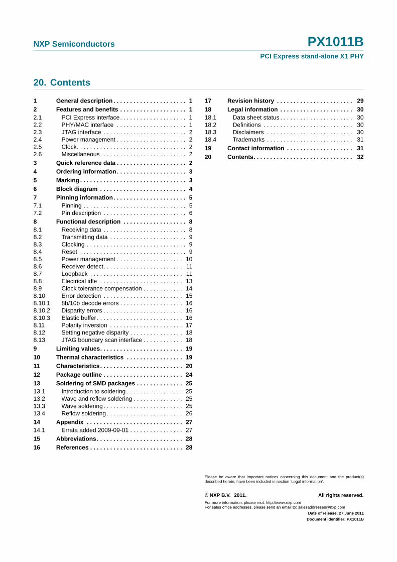
20. Contents
1 General description . . . . . . . . . . . . . . . . . . . . . . 1
2 Features and benefits . . . . . . . . . . . . . . . . . . . . 12.1 PCI Express interface. . . . . . . . . . . . . . . . . . . . 12.2 PHY/MAC interface . . . . . . . . . . . . . . . . . . . . . 12.3 JTAG interface . . . . . . . . . . . . . . . . . . . . . . . . . 22.4 Power management . . . . . . . . . . . . . . . . . . . . . 22.5 Clock. . . . . . . . . . . . . . . . . . . . . . . . . . . . . . . . . 22.6 Miscellaneous. . . . . . . . . . . . . . . . . . . . . . . . . . 2
3 Quick reference data . . . . . . . . . . . . . . . . . . . . . 2
4 Ordering information. . . . . . . . . . . . . . . . . . . . . 3
5 Marking . . . . . . . . . . . . . . . . . . . . . . . . . . . . . . . . 3
6 Block diagram . . . . . . . . . . . . . . . . . . . . . . . . . . 4
7 Pinning information. . . . . . . . . . . . . . . . . . . . . . 57.1 Pinning . . . . . . . . . . . . . . . . . . . . . . . . . . . . . . . 57.2 Pin description . . . . . . . . . . . . . . . . . . . . . . . . . 6
8 Functional description . . . . . . . . . . . . . . . . . . . 88.1 Receiving data . . . . . . . . . . . . . . . . . . . . . . . . . 88.2 Transmitting data . . . . . . . . . . . . . . . . . . . . . . . 98.3 Clocking . . . . . . . . . . . . . . . . . . . . . . . . . . . . . . 98.4 Reset . . . . . . . . . . . . . . . . . . . . . . . . . . . . . . . . 98.5 Power management . . . . . . . . . . . . . . . . . . . . 108.6 Receiver detect. . . . . . . . . . . . . . . . . . . . . . . . 118.7 Loopback . . . . . . . . . . . . . . . . . . . . . . . . . . . . 118.8 Electrical idle . . . . . . . . . . . . . . . . . . . . . . . . . 138.9 Clock tolerance compensation . . . . . . . . . . . . 148.10 Error detection . . . . . . . . . . . . . . . . . . . . . . . . 158.10.1 8b/10b decode errors . . . . . . . . . . . . . . . . . . . 168.10.2 Disparity errors . . . . . . . . . . . . . . . . . . . . . . . . 168.10.3 Elastic buffer . . . . . . . . . . . . . . . . . . . . . . . . . . 168.11 Polarity inversion . . . . . . . . . . . . . . . . . . . . . . 178.12 Setting negative disparity . . . . . . . . . . . . . . . . 188.13 JTAG boundary scan interface . . . . . . . . . . . . 18
9 Limiting values. . . . . . . . . . . . . . . . . . . . . . . . . 19
10 Thermal characteristics . . . . . . . . . . . . . . . . . 19
11 Characteristics. . . . . . . . . . . . . . . . . . . . . . . . . 20
12 Package outline . . . . . . . . . . . . . . . . . . . . . . . . 24
13 Soldering of SMD packages . . . . . . . . . . . . . . 2513.1 Introduction to soldering . . . . . . . . . . . . . . . . . 2513.2 Wave and reflow soldering . . . . . . . . . . . . . . . 2513.3 Wave soldering . . . . . . . . . . . . . . . . . . . . . . . . 2513.4 Reflow soldering . . . . . . . . . . . . . . . . . . . . . . . 26
14 Appendix . . . . . . . . . . . . . . . . . . . . . . . . . . . . . 2714.1 Errata added 2009-09-01 . . . . . . . . . . . . . . . . 27
15 Abbreviations. . . . . . . . . . . . . . . . . . . . . . . . . . 28
16 References . . . . . . . . . . . . . . . . . . . . . . . . . . . . 28
17 Revision history . . . . . . . . . . . . . . . . . . . . . . . 29
18 Legal information . . . . . . . . . . . . . . . . . . . . . . 3018.1 Data sheet status . . . . . . . . . . . . . . . . . . . . . . 3018.2 Definitions . . . . . . . . . . . . . . . . . . . . . . . . . . . 3018.3 Disclaimers . . . . . . . . . . . . . . . . . . . . . . . . . . 3018.4 Trademarks . . . . . . . . . . . . . . . . . . . . . . . . . . 31
19 Contact information . . . . . . . . . . . . . . . . . . . . 31
20 Contents. . . . . . . . . . . . . . . . . . . . . . . . . . . . . . 32
© NXP B.V. 2011. All rights reserved.
For more information, please visit: http://www.nxp.comFor sales office addresses, please send an email to: [email protected]
Date of release: 27 June 2011
Document identifier: PX1011B
Please be aware that important notices concerning this document and the product(s)described herein, have been included in section ‘Legal information’.