Embed Size (px)
Citation preview

Solution Proposal by Toshiba
© 2019-2021 Toshiba Electronic Devices & Storage Corporation
PV Inverter forHousehold Use
R20

© 2019-2021 Toshiba Electronic Devices & Storage Corporation
Toshiba Electronic Devices & Storage Corporation provides comprehensive device solutions to customers developing new products by applying its thorough understanding of the systems acquired through the analysis of basic product designs.

BlockDiagram
© 2019-2021 Toshiba Electronic Devices & Storage Corporation

4© 2019-2021 Toshiba Electronic Devices & Storage Corporation
PV Inverter for Household Use Overall block diagram
JunctionBox
IsolationAmp
IsolationAmp
IsolationAmp
AC Noise Filter
Boost Chopper Inverter CircuitPhase Current
Monitoring
BUS Voltage Monitoring
Network I/ORS-485, etc.Fan / Display
Solar PanelSolar PanelSolar Panel
MCU
DC-DC MCU, Photocoupler, Isolation Amp, etc.
Isolation
Isolation MOSFET Isolation MOS
FET
MOSFET
MOSFET
MOSFET
Isolation
Isolation Isolation

5© 2019-2021 Toshiba Electronic Devices & Storage Corporation
Boost ChopperCircuit Three-phase
AC Output
Two-phase AC Output
Photocoupler
Photocoupler
Photocoupler
Photocoupler
ACNoiseFilter
Current Transformer
IsolationAmp
Op-amp
IsolationAmp
Op-amp
MCU
Current Transformer
MOSFET
MOSFET
MOSFET
MOSFET
Inverter Circuit
Solar PanelSolar Panel
Solar Panel
JunctionBox Photo
coupler
Current Transformer
MCUIsolationAmp Op-amp
PV Inverter for Household Use Details of power supply unitCriteria for device selection- Inverter output (output Low with LED signal ON)
is suitable for low active IPM, and high speed is required for PWM signal transmission.
- To improve the efficiency of the inverter, it is important to select a MOSFET with a balanced on- resistance and switching speed.
- Isolation amplifier is suitable for detecting signals with different reference potentials.
- Signal amplification with high accuracy requires low noise performance.
- Efficient inverter control is required.
Proposals from Toshiba- Photocoupler with excellent environmental resistance
IC output photocoupler
- Low on-resistance and high speed switching MOSFETDTMOS Series MOSFET
- Photocoupler with excellent environmental resistanceIsolation amplifier
- Amplify the detected weak signal with low noiseLow noise operational amplifier
- Built-in three-phase PWM is suitable for controlling inverter systemMCU
3
Boost converter circuit
1
1
Inverter circuit
3
4
4
1 1
1 13
4
43
※ Click on the number in the circuit diagram to jump to the detailed description page5
5
2 2
2 22

RecommendedDevices
© 2019-2021 Toshiba Electronic Devices & Storage Corporation

7© 2019-2021 Toshiba Electronic Devices & Storage Corporation
Device solutions to address customer needs
As described above, in the design of PV inverter for household use, “Enhancement of safety of the set”, “High efficiency” and “Miniaturization of circuit boards” are important factors. Toshiba’s proposals are based on these three solution perspectives.
Safety Small sizepackagesLow loss
Enhancement ofsafety of the set High efficiency Miniaturization
of circuit boards

8© 2019-2021 Toshiba Electronic Devices & Storage Corporation
Device solutions to address customer needs
IC output photocoupler
Isolation amplifierLow noise operational amplifier
1
3
4
Safety Low loss Small sizepackages
MCU5
DTMOS Series MOSFET2

Line up
Value provided
9© 2019-2021 Toshiba Electronic Devices & Storage Corporation
This photocoupler optically couples an infrared light emitting diode with high optical output power and an integrated circuit light-receiving IC chip with high gain and high speed.
For low active IPMCommon-mode transient immunity (CMTI) of 10 [kV/μs]
High speed and small delay time variations
Inverter output (output Low with LED signal ON) is supported for low active IPM driving.
High CMTI is required because a high dV/dt is applied to the control signal terminal of the IPM. This photocoupler has CMTI capability of 10 [kV/μs] or more by providing shield between input and output of the photocoupler.
IPM drive photocouplers transmit PWM signals, which requires high speed operation.
Internal circuit configuration
IC output photocouplerTLP2719(LF4)
Safety Low loss Small sizepackages1a
◆ Return to Block Diagram Top
Part number TLP2719(LF4)
Package SO6L(LF4)
BVS (Min) [Vrms] 5000
NRZ (Typ.) [Mbps] 1
CMH, CML (Min) [kV/μs] ±10

Line up
Value provided
10© 2019-2021 Toshiba Electronic Devices & Storage Corporation
The built-in various protective functions make it easy to design the gate drive circuit.
Protective functions Rail-to-rail output High temperature of 110 °C(ambient) operation
Various protective functions[note] including an overcurrent detection by monitoring collector voltage are built in. [note] Gate signal soft turn off, fault feedback function
TLP5231, TLP5214 and TLP5214A generate a full-swing voltage output signal and contribute to low power consumption
These photocouplers are designed to operate under severe ambient temperature conditions.
IC output photocouplerTLP5231 / TLP5214 / TLP5214A (Smart Gate Driver Coupler)
Safety Low loss Small sizepackages1b
◆ Return to Block Diagram Top
Recommended Application Circuit (TLP5231)
Part number TLP5231 TLP5214 TLP5214A
Package SO16L SO16L SO16L
IOP (Max) [A] ±2.5 ±4.0 ±4.0tpHL/tpLH (Max) [ns] 300 150 150
BVS [Vrms] 5000 5000 5000Topr [°C] -40 to 110 -40 to 110 -40 to 110
VCC2 – VEE [V] 21.5 to 30 15 to 30 15 to 30IFHL(IFLH) (Max) [mA] 3.5 6 6
DESAT Filter ✔ ✔
Line up
Value provided
11© 2019-2021 Toshiba Electronic Devices & Storage Corporation
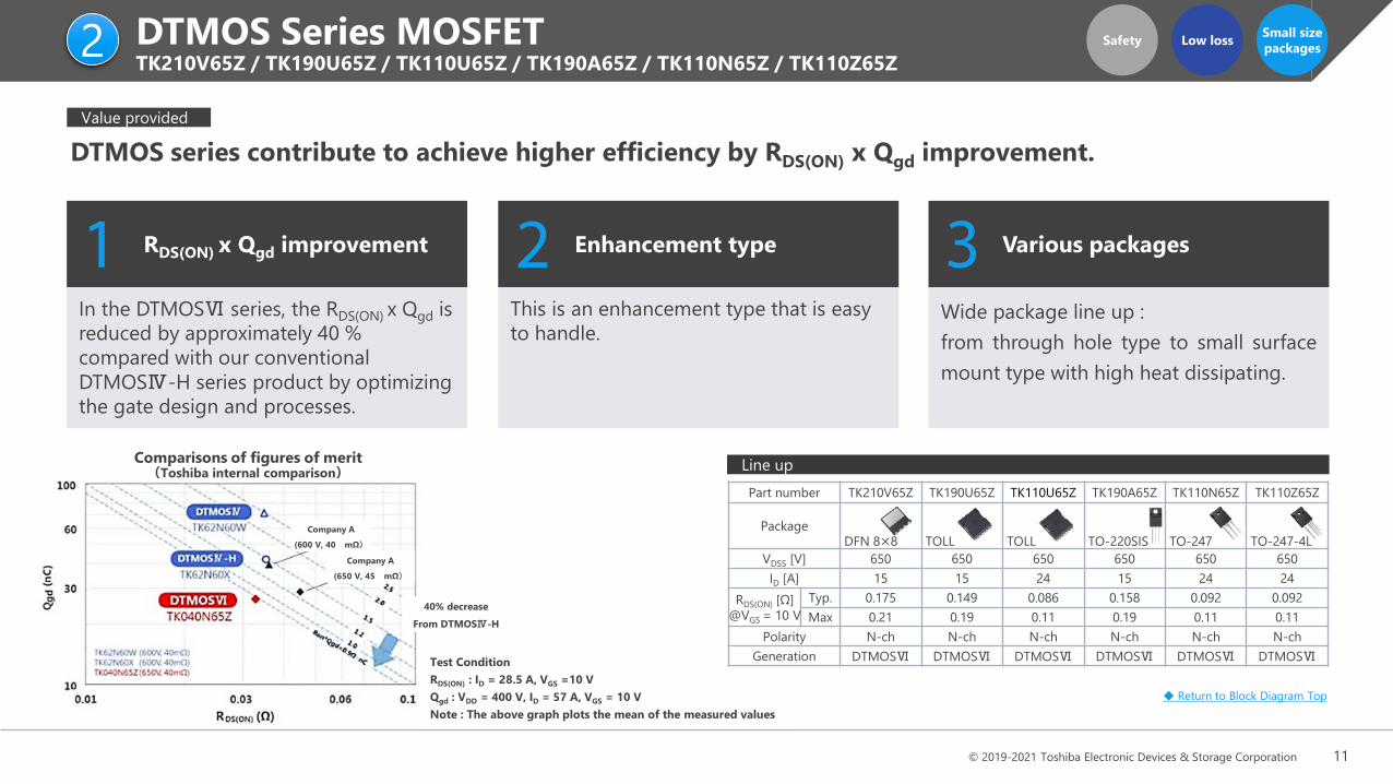
Test ConditionRDS(ON) : ID = 28.5 A, VGS =10 VQgd : VDD = 400 V, ID = 57 A, VGS = 10 VNote : The above graph plots the mean of the measured values
DTMOS series contribute to achieve higher efficiency by RDS(ON) x Qgd improvement.
RDS(ON) x Qgd improvement Enhancement type Various packages
In the DTMOSⅥ series, the RDS(ON) x Qgd is reduced by approximately 40 % compared with our conventional DTMOSⅣ-H series product by optimizing the gate design and processes.
This is an enhancement type that is easy to handle.
Wide package line up :from through hole type to small surfacemount type with high heat dissipating.
DTMOS Series MOSFETTK210V65Z / TK190U65Z / TK110U65Z / TK190A65Z / TK110N65Z / TK110Z65Z
Small sizepackages2
◆ Return to Block Diagram Top
Safety Low loss
40% decreaseFrom DTMOSⅣ-H
Company A
(650 V, 45 mΩ)
Company A
(600 V, 40 mΩ)
Comparisons of figures of merit(Toshiba internal comparison)
Part number TK210V65Z TK190U65Z TK110U65Z TK190A65Z TK110N65Z TK110Z65Z
PackageDFN 8×8 TOLL TOLL TO-220SIS TO-247 TO-247-4L
VDSS [V] 650 650 650 650 650 650ID [A] 15 15 24 15 24 24
RDS(ON) [Ω]@VGS = 10 V
Typ. 0.175 0.149 0.086 0.158 0.092 0.092Max 0.21 0.19 0.11 0.19 0.11 0.11
Polarity N-ch N-ch N-ch N-ch N-ch N-chGeneration DTMOSⅥ DTMOSⅥ DTMOSⅥ DTMOSⅥ DTMOSⅥ DTMOSⅥ

Line up
Value provided
12© 2019-2021 Toshiba Electronic Devices & Storage Corporation
Isolation amplifier with low current consumption and compact package enables highly accuratecurrent detection.
Low current consumptionLow height compact package
High accuracy
Introduction of new digital modulation technology has reduced current consumption due to input voltage dependence.
Compact and low profile (2.3 [mm] (Max)) SO8L package contributes reducingmounting area.
This optical coupling type isolation amplifier uses an IC with a high precision ΔΣ A/D convertor circuit on the input side and an IC with a high precision D/A convertor circuit on the output side.
Part number TLP7820
Package SO8L(LF4)
Gain accuracy [%] ±0.5 / ±1.0 / ±3.0 (rank selection)|dG/dTa| (Typ.) [V/V/°C] 0.00012
NL200 (Typ.) [%] 0.02VOS (Typ.) [mV] 0.9IDD1 (Typ.) [mA] 8.6IDD2 (Typ.) [mA] 6.2
Current consumption characteristics
Isolation amplifierTLP78203 Safety Low loss Small size
packages
◆ Return to Block Diagram Top
(Based on Toshiba’s measurement data)

Line up
Value provided
13© 2019-2021 Toshiba Electronic Devices & Storage Corporation
Very small signals detected by various sensors can be amplified with very low noise.
Low noiseVNI=6.0 [nV/√Hz](Typ.)@f=1 kHz
Low current consumptionIDD=430 [μA](Typ.)
Low supply voltage operation
Very small signals detected by various sensors [Note 1] can be amplify with low noise using CMOS operational amplifier by optimizing the processing. We achieved one of the industry’s lowest [Note 2] input equivalent noise voltage.
The low current consumption characteristics of CMOS processing contributes to the extension of battery life of the compact IoT devices.
VDD = 2.2 to 5.5 V
Low noise operational amplifierTC75S67TU4 Safety Low loss Small size
packages
◆ Return to Block Diagram Top
Low noisecharacteristic
(Toshiba internal comparison)
[Note 1] Sensor types: vibration detection sensor, shock sensor, accelerometer, pressure sensor, infrared sensor, and temperature sensor, etc.[Note 2] Based on Toshiba data (as of May 2017)
Equi
vale
nt in
put n
oise
vol
tage
VN
I
(nV/
√Hz)
Frequency f(Hz)VNI - f
Conventional products :TC75S63TU
TC75S67TU
Part number TC75S67TU
Package UFV
VDD,SS (Max) [V] ±2.75
VDD,SS (Min) [V] ±1.1
IDD (Typ. / Max) [μA] 430 / 700 (@VDD = 2.5 V)
VNI (Typ.) [nV/√Hz] @f=1 kHz 6

Line up
Value provided
14© 2019-2021 Toshiba Electronic Devices & Storage Corporation
MCUTX03 Series M380 Group TMPM381FWFG / TMPM383FSUG
Toshiba original oscillation frequency detector (OFD) can be utilized for abnormal operation detection of system.
Built-in Arm® Cortex®-M3 CPU core
System cost down and development efficiency improvement
Built-in oscillation frequency detector
TMPM381/383 implements Cortex-M3 core with 40 MHz maximum operation frequency. Various development tool and their partners allow users many options.
TMPM381/383 executes system monitoring efficiently by using built-in ADC. The original NANOFLASH™ is possible to rewrite at high speed. It reduces user software development time period.
TMPM381/383 implements Toshiba original oscillation frequency detector (OFD) which detects abnormal oscillation at the hardware level. This function can be utilized for abnormal operation detection of system.
5
◆ Return to Block Diagram Top
Safety Low loss Small sizepackages
TMPM381FWFG TMPM383FSUGPart Number TMPM381FWFG TMPM383FSUG
Maximum operation frequency 40 MHz 40 MHzInstruction ROM 128 KB 64 KB
RAM 10 KB 8 KBTimer 16bit x 14ch 16bit x 8ch
UART / SIO 3ch 2chFull UART 1ch 1ch
ADC 18ch (12bit) 10ch (12bit)IO Port 83 ports 47 ports

© 2019-2021 Toshiba Electronic Devices & Storage Corporation
If you are interested in these products andhave questions or comments about any of them,please do not hesitate to contact us below:
Contact address: https://toshiba.semicon-storage.com/ap-en/contact.html

16© 2019-2021 Toshiba Electronic Devices & Storage Corporation
Terms of useThis terms of use is made between Toshiba Electronic Devices and Storage Corporation (“We”) and customers who use documents and data that are consulted to design electronics applications on which our semiconductor devices are mounted (“this Reference Design”). Customers shall comply with this terms of use. Please note that it is assumed that customers agree to any and all this terms of use if customers download this Reference Design. We may, at its sole and exclusive discretion, change, alter, modify, add, and/or remove any part of this terms of use at any timewithout any prior notice. We may terminate this terms of use at any time and for any reason. Upon termination of this terms of use, customers shall destroy this Reference Design. In the event of any breach thereof by customers, customers shall destroy this Reference Design, and furnish us a written confirmation to prove such destruction.
1. Restrictions on usage1.This Reference Design is provided solely as reference data for designing electronics applications. Customers shall not use this Reference Design for any other purpose, including without
limitation, verification of reliability.2.This Reference Design is for customer's own use and not for sale, lease or other transfer.3.Customers shall not use this Reference Design for evaluation in high or low temperature, high humidity, or high electromagnetic environments.4.This Reference Design shall not be used for or incorporated into any products or systems whose manufacture, use, or sale is prohibited under any applicable laws or regulations.
2. Limitations1.We reserve the right to make changes to this Reference Design without notice.2.This Reference Design should be treated as a reference only. We are not responsible for any incorrect or incomplete data and information.3.Semiconductor devices can malfunction or fail. When designing electronics applications by referring to this Reference Design, customers are responsible for complying with safety standards
and for providing adequate designs and safeguards for their hardware, software and systems which minimize risk and avoid situations in which a malfunction or failure of semiconductor devices could cause loss of human life, bodily injury or damage to property, including data loss or corruption. Customers must also refer to and comply with the latest versions of all relevant our information, including without limitation, specifications, data sheets and application notes for semiconductor devices, as well as the precautions and conditions set forth in the "Semiconductor Reliability Handbook".
4.When designing electronics applications by referring to this Reference Design, customers must evaluate the whole system adequately. Customers are solely responsible for all aspects of their own product design or applications. WE ASSUME NO LIABILITY FOR CUSTOMERS' PRODUCT DESIGN OR APPLICATIONS.
5.No responsibility is assumed by us for any infringement of patents or any other intellectual property rights of third parties that may result from the use of this Reference Design. No license to any intellectual property right is granted by this terms of use, whether express or implied, by estoppel or otherwise.
6.THIS REFERENCE DESIGN IS PROVIDED "AS IS". WE (a) ASSUME NO LIABILITY WHATSOEVER, INCLUDING WITHOUT LIMITATION, INDIRECT, CONSEQUENTIAL, SPECIAL, OR INCIDENTAL DAMAGES OR LOSS, INCLUDING WITHOUT LIMITATION, LOSS OF PROFITS, LOSS OF OPPORTUNITIES, BUSINESS INTERRUPTION AND LOSS OF DATA, AND (b) DISCLAIM ANY AND ALL EXPRESS OR IMPLIED WARRANTIES AND CONDITIONS RELATED TO THIS REFERENCE DESIGN, INCLUDING WARRANTIES OR CONDITIONS OF MERCHANTABILITY, FITNESS FOR A PARTICULAR PURPOSE, ACCURACY OF INFORMATION, OR NONINFRINGEMENT.
3. Export ControlCustomers shall not use or otherwise make available this Reference Design for any military purposes, including without limitation, for the design, development, use, stockpiling or manufacturing of nuclear, chemical, or biological weapons or missile technology products (mass destruction weapons). This Reference Design may be controlled under the applicable export laws and regulations including, without limitation, the Japanese Foreign Exchange and Foreign Trade Law and the U.S. Export Administration Regulations. Export and re-export of this Reference Design are strictly prohibited except in compliance with all applicable export laws and regulations.
4. Governing LawsThis terms of use shall be governed and construed by laws of Japan.

17© 2019-2021 Toshiba Electronic Devices & Storage Corporation
RESTRICTIONS ON PRODUCT USE• Toshiba Electronic Devices & Storage Corporation, and its subsidiaries and affiliates (collectively "TOSHIBA"), reserve the right to make changes to the information in this document, and related
hardware, software and systems (collectively "Product") without notice. • This document and any information herein may not be reproduced without prior written permission from TOSHIBA. Even with TOSHIBA's written permission, reproduction is permissible only if
reproduction is without alteration/omission.• Though TOSHIBA works continually to improve Product's quality and reliability, Product can malfunction or fail. Customers are responsible for complying with safety standards and for providing
adequate designs and safeguards for their hardware, software and systems which minimize risk and avoid situations in which a malfunction or failure of Product could cause loss of human life, bodily injury or damage to property, including data loss or corruption. Before customers use the Product, create designs including the Product, or incorporate the Product into their own applications, customers must also refer to and comply with (a) the latest versions of all relevant TOSHIBA information, including without limitation, this document, the specifications, the data sheets and application notes for Product and the precautions and conditions set forth in the "TOSHIBA Semiconductor Reliability Handbook" and (b) the instructions for the application with which the Product will be used with or for. Customers are solely responsible for all aspects of their own product design or applications, including but not limited to (a) determining the appropriateness of the use of this Product in such design or applications; (b) evaluating and determining the applicability of any information contained in this document, or in charts, diagrams, programs, algorithms, sample application circuits, or any other referenced documents; and (c) validating all operating parameters for such designs and applications. TOSHIBA ASSUMES NO LIABILITY FOR CUSTOMERS' PRODUCT DESIGN OR APPLICATIONS..
• PRODUCT IS NEITHER INTENDED NOR WARRANTED FOR USE IN EQUIPMENTS OR SYSTEMS THAT REQUIRE EXTRAORDINARILY HIGH LEVELS OF QUALITY AND/OR RELIABILITY, AND/OR A MALFUNCTION OR FAILURE OF WHICH MAY CAUSE LOSS OF HUMAN LIFE, BODILY INJURY, SERIOUS PROPERTY DAMAGE AND/OR SERIOUS PUBLIC IMPACT ("UNINTENDED USE"). Except for specific applications as expressly stated in this document, Unintended Use includes, without limitation, equipment used in nuclear facilities, equipment used in the aerospace industry, lifesaving and/or life supporting medical equipment, equipment used for automobiles, trains, ships and other transportation, traffic signaling equipment, equipment used to control combustions or explosions, safety devices, elevators and escalators, and devices related to power plant. IF YOU USE PRODUCT FOR UNINTENDED USE, TOSHIBA ASSUMES NO LIABILITY FOR PRODUCT. For details, please contact your TOSHIBA sales representative or contact us via our website.
• Do not disassemble, analyze, reverse-engineer, alter, modify, translate or copy Product, whether in whole or in part.• Product shall not be used for or incorporated into any products or systems whose manufacture, use, or sale is prohibited under any applicable laws or regulations.• The information contained herein is presented only as guidance for Product use. No responsibility is assumed by TOSHIBA for any infringement of patents or any other intellectual property rights
of third parties that may result from the use of Product. No license to any intellectual property right is granted by this document, whether express or implied, by estoppel or otherwise.• ABSENT A WRITTEN SIGNED AGREEMENT, EXCEPT AS PROVIDED IN THE RELEVANT TERMS AND CONDITIONS OF SALE FOR PRODUCT, AND TO THE MAXIMUM EXTENT ALLOWABLE
BY LAW, TOSHIBA (1) ASSUMES NO LIABILITY WHATSOEVER, INCLUDING WITHOUT LIMITATION, INDIRECT, CONSEQUENTIAL, SPECIAL, OR INCIDENTAL DAMAGES OR LOSS, INCLUDING WITHOUT LIMITATION, LOSS OF PROFITS, LOSS OF OPPORTUNITIES, BUSINESS INTERRUPTION AND LOSS OF DATA, AND (2) DISCLAIMS ANY AND ALL EXPRESS OR IMPLIED WARRANTIES AND CONDITIONS RELATED TO SALE, USE OF PRODUCT, OR INFORMATION, INCLUDING WARRANTIES OR CONDITIONS OF MERCHANTABILITY, FITNESS FOR A PARTICULAR PURPOSE, ACCURACY OF INFORMATION, OR NONINFRINGEMENT.
• Product may include products using GaAs (Gallium Arsenide). GaAs is harmful to humans if consumed or absorbed, whether in the form of dust or vapor. Handle with care and do not break, cut, crush, grind, dissolve chemically or otherwise expose GaAs in Product.
• Do not use or otherwise make available Product or related software or technology for any military purposes, including without limitation, for the design, development, use, stockpiling or manufacturing of nuclear, chemical, or biological weapons or missile technology products (mass destruction weapons). Product and related software and technology may be controlled under the applicable export laws and regulations including, without limitation, the Japanese Foreign Exchange and Foreign Trade Law and the U.S. Export Administration Regulations. Export and re-export of Product or related software or technology are strictly prohibited except in compliance with all applicable export laws and regulations.
• Please contact your TOSHIBA sales representative for details as to environmental matters such as the RoHS compatibility of Product. Please use Product in compliance with all applicable laws and regulations that regulate the inclusion or use of controlled substances, including without limitation, the EU RoHS Directive. TOSHIBA ASSUMES NO LIABILITY FOR DAMAGES OR LOSSES OCCURRING AS A RESULT OF NONCOMPLIANCE WITH APPLICABLE LAWS AND REGULATIONS.

* Arm and Cortex are registered trademarks of Arm Limited (or its subsidiaries) in the US and/or elsewhere.* NANOFLASHTM is a trademark of Toshiba Electronic Devices & Storage Corporation.* All other company names, product names, and service names may be trademarks of their respective companies.