Embed Size (px)
Citation preview

Pushpull Power Amplifiers for HandsetsTom Apel and Jun Zhao
Technology Development
Abstract — Design of pushpull power amplifiers forhandset applications is presented. Development ofbalanced transformers and baluns is detailed. ICrealization techniques, such as interleaving of outputtransistor cells, are also presented. Examples arepresented in cellular band and PCS in addition to awideband PA that spans more than an octave (0.8 GHzto 2 GHz).
Index Terms — Pushpull, baluns, power amplifiers.
I. INTRODUCTION
Handset power amplifier performance targetscontinue to become more challenging. Linearity andpower efficiency performance that was competitivetwo years ago will not be in the future. The challengeis further compounded by system demands for morebandwidth and the desire to have power amplifierssupport multiple (all) operating modulation modes.Both multiple mode and multiple band interests aredriven by cost reduction considerations.
The most significant design aspect leading tohandset power amplifier performance limitations isthe low load impedance required to support theoutput power requirement from a low voltage DCsupply. As operating voltage is lowered, severaleffects conspire to reduce power efficiency. First,knee voltage drop in the transistor, at high current,represents a larger fraction of the available peakvoltage (set by the DC supply). For a given poweroutput, as the peak voltage is reduced, thecorresponding current must increase. This loweringof load impedance leads to the second contribution toperformance reduction. The output matching networkmust transform the external 50 load to the lowimpedance load at the transistor. Loss increases astransformation ratio is increased. Bandwidth isalmost always compromised as load impedances arelowered.
Several general principals are suggested: 1) raisethe operating voltage whenever you can, and 2)reduce the impedance transformation ratio in thematching network whenever you can. The supplyvoltage to the PA could be raised by a DC-DC boostconverter. However, this isn’t always possible. Areduction in transformation ratio is possible without
changing the DC supply voltage. By departing fromconventional “all cells in parallel” single-endedthinking, we can gain a four-fold advantage intransformation ratio reduction from differential (alsocalled pushpull) operation. An example of this type ofPA can be seen in Figs. 1 and 2. The chip photo inFig.1 shows a two stage PA with integrated baluninput. The laminate module photo in Fig.2 provides alow loss balun to impedance match the PA die.
Fig.1. Cellular pushpull PA die
Fig.2. Cellular pushpull PA module

II. ADVANTAGES OF DIFFERENTIAL OPERATION
If one considers all transistor segments operating inphase as single-ended, then the conceptual partitionof those cells into two clusters can be useful in viewof the relationship between single-ended anddifferential (also called pushpull). Proper load sharingwould suggest both clusters see the same load, 2xthe external load. The RF current flowing througheach cluster is half of the total and the same RFvoltage is seen by all cells in parallel. As analternative, if we operate the same two clusters ofcells out of phase by 180 degrees, then each mustsee the same optimum load. The RF voltages andcurrents are; however, 180 degrees out of phase.The total load voltage is twice the voltage across anindividual cluster, while the total current is the same.In other words, the external differential load is twicethat of one cluster. So, the differential load is fourtimes the single-ended load for the same number ofcells, supply voltage, and power output! Thissignificant advantage is illustrated in Fig.3.
Fig.3. Relationship between single-endedloading and pushpull loading.
At this point, in order to avoid confusion, it isimportant to recognize that several terms aresynonymous. Differential mode, odd mode orpushpull operation all have the same meaning inpushpull amplifiers. Similarly, common mode, evenmode, and single-ended operation may beinterchanged.
Both sides of pushpull amplifiers are usually biasedfrom a common bias source. So, from a DCperspective, operation is in parallel (common mode).When distortion produces harmonics, odd order
Fourier terms maintain differential mode symmetry,while even order Fourier terms appear in thecommon mode. This additional degree of freedomprovided within pushpull amplifiers can be used toconsiderable advantage. While maintaining balancein the differential mode, a natural suppression ofsecond harmonic levels from the output is present. Itis important to point out that this applies to secondharmonic levels generated in the pushpull PA stage.Any drive from previous stages at second harmonicfrequencies will, of course, be amplified like any otherodd mode input signal.
Some of the advantages pushpull PAs offerover single-ended PAs are:
1) Four times greater load impedance for givenpower and supply voltage,
2) Separation of even and odd harmonicfrequency terms,
3) Elimination of high current in a common modebypass path,
4) Significant reduction in RF ground currents,5) Means to provide 2nd harmonic short over a
broad band for linear amplifiers,6) Reduction in 2nd harmonic levels due to
common mode isolation,7) Isolation of RF from bias circuit due to common
mode isolation,8) BW performance more readily achieved due to
higher impedance operation.
III. CHALLENGES
One well might ask, if pushpull has so manyadvantages, why isn’t it in widespread use in handsetapplications? It is very much in widespread use atlower frequencies (3 MHz through 450 MHz). It isalso used in some high power pulsed avionics and insome cellular base station PAs. In all cases, theenabling circuit element is a low loss balun in theoutput circuit. For handset applications, this mustalso be small enough for module integration. Losshas been the roadblock for acceptably small baluns.Lack of such an element has been the primaryimpediment to pushpull PA development for handsetapplications. Low frequency balun and balancedtransformer implementations are not well suited foruse in handsets. They are usually formed fromtwisted wire pairs or small coax lengths and oftenferrite loaded. A direct use of these techniques is toolarge and limited in upper frequency. Small surfacemount baluns, such as those sold by mini-circuits are

too lossy for competitive handset power amplifiers.Losses should be under 0.5 dB and the size of theoverall output match should at least be competitivewith current single-ended matches.
Input baluns should be integrated into the PA IC.Similarly, the interstage match in the IC should havean integrated balanced transformer.
Since balanced transformers and baluns are thegating elements in successful pushpull poweramplifiers for handsets, they will be discussed next.
IV. BALANCED TRANSFORMERS AND BALUNS
Transformers can be realized in classic form wherethe only coupling mechanism is magnetic flux, or ascomposites of coupled transmission line unit blocks.Examples of the transmission line transformers aresingle-ended Ruthroff [1] and balanced Guanella [2]transformers [3,4].
Classic flux coupled transformers are comprised ofseparate tightly coupled inductors. For low loss andwide bandwidth, coupling near unity (k>0.9) isdesired. Distributed capacitance causes selfresonance and kills high frequency performance.
Transmission line transformers are comprised ofsegments of coupled transmission lines. Unlike theclassic flux (only) coupled transformers, the finiteimpedance of the transmission line provides a naturalmechanism for dealing with non zero, real world,distributed capacitance. Losses are also lower, for agiven media, due to energy coupling by both fluxcoupling and by a conducted path. For both of thesereasons, one can confidently say that transmissionline transformers will always outperform flux (only)coupled transformers in the same media.
Before we jump into a discussion of balancedtransformers (sometimes called balbal structures)and balanced to unbalanced transformers (alsocalled balun structures), let’s look at single-endedcases. Fig.4 illustrates a single-ended transformerfrom both cases. Conventional transformers provideimpedance transformation proportional to the squareof the turns ratio. Voltage ratios follow the turns ratioand current ratios are inversely proportional to theturns ratio. Transmission line transformers arecomprised of unit elements that are oftenrepresented as 1:1 transformers. Flux couplingrequires equal and opposite directed currents inthese unit element lines. By inspection, we can seethat the Ruthroff transformer in Fig.4 provides doublethe current at the right port, with half the voltage
Fig.4 Single-ended transformers:transmission line type (4:1), and conventionalflux coupled.
compared to the left port. This is an example of asingle-ended 4:1 transmission line transformer.
If we wish to make a balanced to unbalancedtransformer (also called a balun), we could simply‘float’ the grounded connection on one side of theconventional transformer shown in Fig.4. Better yet,we could ground a center tap on the balanced side(to better force the balance). This can be seen inFig.5.
Fig.5 Conventional balanced to unbalancedtransformer (BALUN).
Since a performance advantage can be obtainedfrom transmission line related transformer structures,the obvious question is “How can one maketransmission line related baluns and balancedtransformers?”. Consider the two cases illustrated inFig.6. Both structures are comprised of coupled lineunit elements. Allowed currents due to magneticcoupling are shown.

ZooZoeZooZoek
Fig.6 Transmission line balun elements.
The “choke balun” structure behaves as atransmission line in the odd mode (between theconductors) to provide low loss energy flow betweenthe ports. This is always true when the currents aredirected equal and opposite, as sketched. Note thatany attempt to launch in-phase common modecurrent into the balance port side is met with a highimpedance inductive termination. Ideally, at unitycoupling, the common mode impedance becomesinfinity. The “choke balun” element provides currentbalance. Only balanced currents are allowed to flow.
The “voltage inverter” can be thought of as a centertaped auto-transformer. Allowed currents are shownin red. Note that these currents are associated withcommon mode currents. This element provides ashort circuit for available common mode current.Ideally, differential mode voltage has no interactionwith this element. The common mode short behaviorprevents any voltage imbalance when the voltageinverter is placed across the balanced port.
By using a combination of choke balun and voltageinverter elements, a very good broadband low loss1:1 balun can be formed. Such a structure will bediscussed in more detail later.
V. FREQUENCY COMPENSATION OF COUPLED LINES
Performance of transmission line unit structurescan be extended by capacitively compensating non-ideal coupling [5]. To explore this, consider the chokebalun shown in Fig.7.
The unit coupled element is best thought of as apair of coupled transmission lines. The odd modeimpedance forms the basis for propagation in thetransmission line mode between the conductors. Forasymmetric lines [6] this is the mode.
Fig.7 Non-Ideal coupling in choke balun
The even mode impedance is a parasitic mode dueto an external ground. The higher the ratio betweeneven mode and odd mode impedance, the greaterthe coupling coefficient. The coupling limit for veryhigh Zoe is unity. This view is useful for optimizingline structures and media choices. Forcompensation, it is useful to consider the inductiveequivalent circuits in Fig.7. In the desired propagationmode, the differential mode inductance, 2(L-M), is tosome extent naturally compensated by the odd modedistributed capacitance in that transmission linemode. This is the capacitance associated with 2·Zoo.The even (parasitic) mode causes low frequencyperformance degradation that requirescompensation. To see this, consider the commonmode equivalent circuit in Fig.7. Clearly, the commonmode balance performance at DC is not good.Rather than an open circuit (high Z inductive), ashunt inductor (L+M) causes a short circuit to ground.A choke balun should deliver power to the balancedport regardless of it’s balance condition. Forexample, if one of the balanced terminals or the otherwas grounded, power flow should not be perturbed.With this ideal performance in mind, consider Fig.8.We have two cases to consider. The first case issimply a transmission line from input to output. Thesecond case is clearly more troublesome, becausethere is no conducted path between input and output
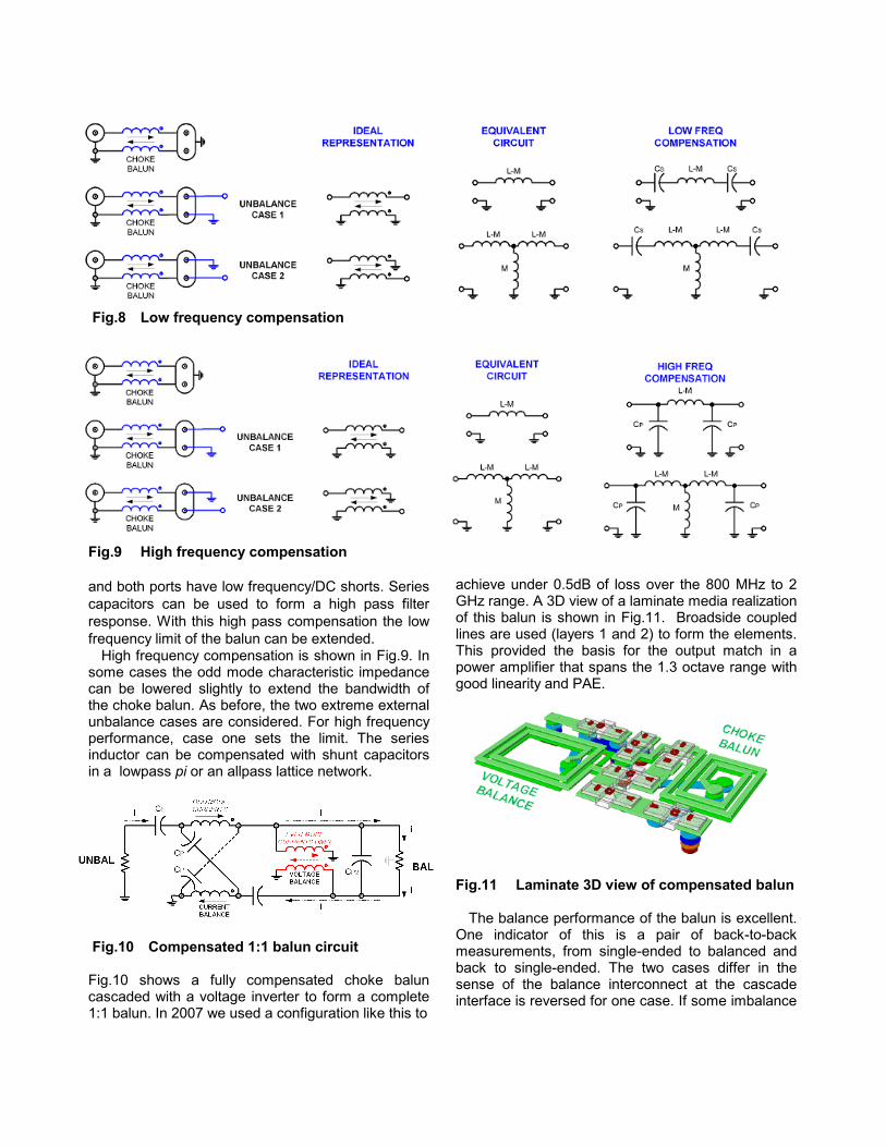
Fig.8 Low frequency compensation
Fig.9 High frequency compensation
and both ports have low frequency/DC shorts. Seriescapacitors can be used to form a high pass filterresponse. With this high pass compensation the lowfrequency limit of the balun can be extended.
High frequency compensation is shown in Fig.9. Insome cases the odd mode characteristic impedancecan be lowered slightly to extend the bandwidth ofthe choke balun. As before, the two extreme externalunbalance cases are considered. For high frequencyperformance, case one sets the limit. The seriesinductor can be compensated with shunt capacitorsin a lowpass pi or an allpass lattice network.
Fig.10 Compensated 1:1 balun circuit
Fig.10 shows a fully compensated choke baluncascaded with a voltage inverter to form a complete1:1 balun. In 2007 we used a configuration like this to
achieve under 0.5dB of loss over the 800 MHz to 2GHz range. A 3D view of a laminate media realizationof this balun is shown in Fig.11. Broadside coupledlines are used (layers 1 and 2) to form the elements.This provided the basis for the output match in apower amplifier that spans the 1.3 octave range withgood linearity and PAE.
Fig.11 Laminate 3D view of compensated balun
The balance performance of the balun is excellent.One indicator of this is a pair of back-to-backmeasurements, from single-ended to balanced andback to single-ended. The two cases differ in thesense of the balance interconnect at the cascadeinterface is reversed for one case. If some imbalance

is present, then one case will be favored. Both wereobserved to be virtually identical.
VI. BALANCED IMPEDANCE TRANSFORMATION
Next we consider the topic of impedancetransformation between balanced loads. Balanced tobalanced (balbal) transformers are necessary withina pushpull amplifier as part of the interstage network.As before, transmission line type structures will bepresented. Later, it will be seen that balancedtransformers paired with choke baluns can be usedto form very good impedance transforming baluns.
The most commonly used balanced transformer isthe Guanella (named after its originator). It provides a4:1 impedance transformation from a pair oftransmission line unit elements. This structure isshown in Fig.12. Common to all transmission linetransformer structures, energy is transferred by both
Fig.12 Guanella 4:1 balanced transformer
a conducted path and through flux coupled unitelements. Once again, as with the Ruthroff single-ended analysis, a current is assumed. In this case itis a differential mode current, I, applied to the port onthe left. The coupled line unit elements require equaland opposite directed currents as illustrated inFig.12. The right hand port clearly has a differentialmode current of 2i. Conservation of energy leads tothe conclusion that this structure provides a 4:1impedance transformation.
The common mode behavior of the Guanella canbe seen in Fig.13. In phase, common mode, currentsare assumed/applied to the port on the left. Coupledline unit elements route these currents to the centerground node. If this node is not grounded, it providesa common mode port.
Fig.13 Guanella common mode current flow
In fact, this structure is a 4-port hybrid similar to awave-guide “magic-T”. To see this, we associate thetwo left side terminals as the two side ports, thecenter tap as the common mode port, and the righthand port is the differential port.
If the Guanella schematic is re-drawn, it’srelationship to a balanced auto-transformer can beseen. Consider the two cases shown in Fig.14.Topologically, the Guanella is the same as aconventional auto-transformer. The primary
Fig.14 Guanella relationship to autotransformer

difference is in the magnetic coupling. The colorcoding from Fig.13 is carried over into Fig.14. Notethat each outer inductive leg is coupled to an innersegment on the other side. The general auto-transformer is does not have this segmentedcoupling. The available impedance ratio is anotherdifference. The Guanella is a 4:1 balancedtransformer, while the auto-transformer can be set toany ratio. The turns ratio is set the fraction of the totalinductance associated with low impedance taps. Theimpedance ratio is the square of the turns ratio. Boththe auto-transformer and the related special case,the Guanella, offer better bandwidth and lossperformance that strictly flux coupled transformers.The tapped inductor is more tightly coupled thanseparate windings, and the conducted path currentsare reasons for this.
Like the voltage inverter in the 1:1 balun, the auto-transformer and Guanella provide a voltage balancewhen the center tap is RF grounded. This leads oneto an impedance transforming balun by replacing thevoltage inverter, in Fig.10, with an auto-transformeror a 4:1 Guanella. This can be seen withcompensation in Fig.15. Of course, the Guanellacould be replaced
Fig.15 Compensated 4:1 balun circuit
with a different ratio auto-transformer. Non-idealbehavior of the transformer, such as leakageinductance, can be compensated by adding shuntcapacitors at both high and low impedance sides.These are labeled Cp1 and Cp2 in Fig.15.
Guanella transformers can be realized in laminatemedia by forming coupled line unit elements withbroadside coupled traces on layers 1 and 2. This canbe seen in Fig.16. If the low impedance taps areseparated, a modified Guanella structure results.This is also illustrated in Fig.16.
The addition of a compensated choke balun, asindicated in Fig.15, leads to practical power amplifieroutput matching networks. We have significantlyreduced the size of the laminate footprint by stackingthe balanced transformer with the choke balun. Thiscan be seen in Fig.17, where the coupled lines forthe choke balun are laterally offset in layers1 and 2,followed by a vertical and lateral offset to traces inlayers 3 and 4.
Fig.16 Laminate 3D view of 2-layer balanced(balbal) transformers
Fig.17 Laminate 3D view of output match(modified Guanella and choke balun)
For yet lower impedance levels a 9:1 auto-transformer can be used with a choke balun. Anexample of a 9:1 balanced transformer, realized inthe top 3 layers of metal of SEMCO’s 6 layer processis show in Fig.18.
Fig.18 Laminate 3D view of 9:1 auto-transformer
When the 9:1 balanced transformer from Fig.18 iscascaded with a compensated choke balun, theoutput network shown in Fig.19 is obtained. Thechoke balun is realized in a broadside coupled pair oflines in layers 1 and 2.

Fig.19 Laminate 3D view of 9:1 output match(auto-transformer and choke balun)
VII. LAMINATE DEVELOPMENT TECHNIQUES
A brief discussion of laminate media developmenttechniques for pushpull output matching networks isnext presented. Figs. 11, 17, and 19 all illustrateoutput matching structures with varioustransformation ratios. One common attribute iscoupled line unit elements are all realized in theupper layers of the metal/dielectric stack. The reasonfor this is coupling coefficient. The transmission linemode between the conductors is used forpropagating desired signals. The characteristicimpedance in this mode is primarily dependent online width and vertical spacing. The parasitictransmission line mode between either conductor andthe backside ground is responsible for limitations incoupling coefficient. Since we don’t have symmetriccoupled lines, a discussion in terms of even and oddmode characteristic impedances isn’t preciselycorrect [5]. The correct mode impedances are called and c. The important point is that the ratio Zoe/Zoo,or for asymmetric cases Zoc/Zo must be large forgood coupling. In a vertical stack of metal anddielectric layers, the distance to the backside groundmust be large compared to the separation betweenthe conductors.
In order to accurately represent the circuit behaviorof the laminate structure, electromagnetic simulationis necessary. Multiport S-parameter files are loadedinto a circuit simulator for analysis of amplifiers.Surface mount component interfaces are bestrepresented by horizontal differential ports. Asstructures become compacted, unintended couplingto adjacent lines becomes significant. One mustconsider alternate cases and run comparisonsimulations. This can be tedious; but, it is necessaryfor compact structures with high performance. Anexample of such a structure can be seen in Fig.17.
VIII. INTEGRATED BALUNS AND BALBALS
In the previous section low loss baluns realized inlaminate were presented. Because losses in theoutput network of a power amplifier are so significantin setting (or limiting) it’s overall performance level,the output baluns were realized off chip. Lower costis also a factor in this choice. The input balun and theinterstage transformer are not severely constrainedto the same extent by loss. Both of these functionshave been successfully integrated into the poweramplifier chip.
The input balun is similar in form to an impedancetransforming balun that was developed on laminatemedia. It consists of a choke balun cascaded with aGuanella balanced transformer. The Guanella in theinput balun is oriented to provide a transformation tohigher impedance for driving the bases of the firststage HBT cells. Fig.20 shows this both in schematicform and in layout. The coupled lines in each of theunit elements are realized as broadside coupled(overlay) traces in metals 1 and 2.
Fig.20 Integrated input balun (choke balun andGuanella)
A Guanella is also used in the cellular bandinterstage match between the final amplifier and thedriver stage collectors. In the PCS interstage, a pairof cascaded Guanella transformers is used to
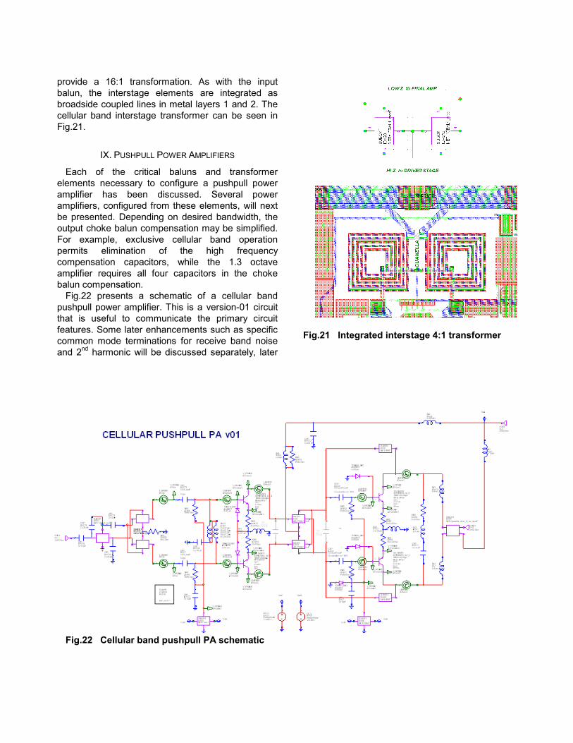
provide a 16:1 transformation. As with the inputbalun, the interstage elements are integrated asbroadside coupled lines in metal layers 1 and 2. Thecellular band interstage transformer can be seen inFig.21.
IX. PUSHPULL POWER AMPLIFIERS
Each of the critical baluns and transformerelements necessary to configure a pushpull poweramplifier has been discussed. Several poweramplifiers, configured from these elements, will nextbe presented. Depending on desired bandwidth, theoutput choke balun compensation may be simplified.For example, exclusive cellular band operationpermits elimination of the high frequencycompensation capacitors, while the 1.3 octaveamplifier requires all four capacitors in the chokebalun compensation.
Fig.22 presents a schematic of a cellular bandpushpull power amplifier. This is a version-01 circuitthat is useful to communicate the primary circuitfeatures. Some later enhancements such as specificcommon mode terminations for receive band noiseand 2nd harmonic will be discussed separately, later
Fig.22 Cellular band pushpull PA schematic
Fig.21 Integrated interstage 4:1 transformer

in this paper. The input balun, interstage transformer,and output balun (4-port S-parameter block) canclearly be seen in relation to the driver and final amptransistors.
The driver stage consists of a pair of 335 um2
mesh (fishbone base) devices. A 1 emitter resistorat each device provides signal degeneration inaddition to some of the overall ballasting. Theremainder of the stage’s thermal stability is providedby the base resistors in the bias circuit path. Thesemust not be set to a value less than 65 for thermalstability reasons. By tailoring the size of this seriesresistance to balance linearity performance betweenmodes, one can achieve an optimum trade-off pointbetween EDGE and UMTS.
The distortion mechanism dominant in UMTSACLR is different than EDGE 400 KHz ACPR. Higherorder IMD terms are more significant in the EDGEcase. This leads to a desire for the bias circuit to notbe a voltage source. UMTS, on the other hand,performance favors a lower impedance biasinterface. The optimum interface to each of the twocells is somewhere between 95 and 150,depending on mode performance preferences. Wereported this bias source impedance relationship tohigher order vs. lower order distortion products in ourearlier “Plain Jane” development with NCDMA, wherewe saw a trade-off in ACPR vs. AltCPR dependenton the base ballast resistor value in stage one.
Bias circuits are conventional closed loop circuitsthat are very similar to those found in the “Plain Jane”amplifiers. One of the clear advantages offered bypushpull operation is the natural isolation betweendrive RF and bias circuits. Bias is fed in a symmetriccommon mode path. Differential mode signals are“balanced out”. This advantage is significant,especially for linear operation.
The series RLC trap between the output stagecollector connections is tuned to the 3rd harmonic.This provides some benefit to linear modeperformance. It is possible because the 3rd harmonicis in the differential mode.
The final amplifier has feedback blocks connectedbetween collector and interstage, on each side.These blocks are tuned to have minimal effect in thedesired operating band; but, to substantially reducegain out of band. The circuit for these 2-port blockscan be seen in Fig.23. The parallel LC resonates inthe operating band. At resonance, the highimpedance minimizes the feedback effect. Atfrequencies out of band the feedback is RC andmuch more aggressive. This is especially important
Fig.23 Feedback in cellular output stage
at lower frequencies where device gain is greater andstability is more of a concern. Rather than lumpingthe series resistance on one end of the network, it issplit into two resistors, one at each end. The transfercharacteristic is the same in both cases; however,the terminal reflection behavior will be different.Consider a case where the feedback connection fromthe collector is routed through the series DC blockingcapacitor followed by the parallel resonator and thenthe series resistor before connecting to the basecapacitor. The interconnect inductance, capacitorfootprint C and the resonator footprint C all cause ashunt capacitive susceptance perturbing the collectortuning. This could easily be an unbalancing effectdue to layout routing and placement constraints. It ismuch safer to isolate the connection at both ends ofthe feedback block from possible unbalance anddetuning with a large series resistor. For this reason,the feedback resistor is split into segments at eachend of the network.
A series RLC can be seen between the differentialoutput nodes of the PA IC. This provides a means ofterminating the 3rd harmonic that also resides in thedifferential mode. This technique allows linearity andPAE to be improved in our cellular PAs. The 3rd
harmonic termination is relatively insensitive with theworst case performance occurring when it views anopen circuit.
The 2nd harmonic termination must be a shortcircuit or minimally inductive. As long as the outputmatching network meets this requirement, the spacebetween the differential output pads (or posts) can beused for a 3rd harmonic trap. If the 2nd harmonicprovided by the output match is not sufficiently closeto a short, then a common mode short must occupythat space on the die. A more detailed discussion ofFourier boundary conditions for optimum pushpullperformance will follow subsequently in this paper.

The schematic in Fig.22 does not show animportant aspect of the final stage array of cells andtheir interface manifolds. Consider the photo shownin Fig.24. The output array consists of 24 cells. Theyare grouped in pairs where adjacent pairs are drivenout of phase. In a manner similar to the “Plain Jane”,the base feed manifold is comprised of lowcharacteristic impedance transmission lines formedfrom metal-dielectric sandwiches (metal-2 / BCB /Metal-1). These structures provide low inductance
Fig.24 Differential output array
Fig.25 Interleaved input manifold
distribution networks for distributing base drivecurrents. By interleaving the feed connectionsbetween alternate pairs of cells, odd mode emittercurrents flow laterally between adjacent pairs ofemitter nodes. This short distance representsapproximately 28 pH (at each interface). The overallodd mode emitter inductance is on the order of 1 pH !This provides a significant gain advantage overconventional single-ended arrays. In the commonmode an effort to provide a uniform emitter returnacross the array, since stable behavior in that modeis also necessary. Fig.25 provides a clear view intothe interleaved base feed.
In Fig.22, the first stage transistor bases areconnected to a voltage inverter (recall Fig.6). Thiselement is intended to have little effect to the desiredpushpull operation. It presents a high odd modeimpedance to the circuit. In contrast, common modevoltages are short circuited to the center tap. Forlinear mode receive-band noise performance, thefirst stage plays a strong role. It is quite important toprovide a low impedance path for low frequencynoise currents from the input stage transistor basesto ground. This prevents efficient up conversion ofnoise from baseband to receive band (conversionoffset from transmit frequency).
X. OPTIMUM FOURIER BOUNDARY CONDITIONS
A detailed analysis of output stage I/O tuning trade-offs was performed in both PCS and cellular bands.The results are plotted in Fig.26. Both cases wererun for Vcc=2.5V. Three performance modes weretracked throughout the many cases considered:UMTS, EDGE, and saturated (for GSM).Fundamental and 3rd harmonic tuning was performedin the odd mode and 2nd harmonic terminations werein the even mode. All other cases (odd order in evenmode and even order in odd mode) were terminatedin an open circuit. Fourier terminating impedancesrepresenting Fundamental, 2nd, and 3rd harmonicsare labeled 1,2, and 3, respectively.
Fundamental frequency output tuning was nosurprise. For higher voltage operation, the realloading level increases approximately with the squareof the supply voltage scaling. Similarly, the shorted2nd harmonic load condition was expected for goodlinear mode performance. The output 3rd harmonictuning was optimum near a short with some inductivereactance. Sensitivity to 3rd harmonic tuning is mild,as long as the open circuit condition is avoided.

Fig.26 Optimum Fourier boundary conditions

Apparently this leads to too much 3rd
harmonic voltage peaking. The 2nd harmonic loadtuning is much more sensitive than that of the 3rd .Fundamental frequency input tuning can be thoughtof as providing two functions. The source’s inductivesusceptance cancels the capacitive behavior of thedevice. The real part provides a basis for broadbandpower transfer. The real part tuning offers animportant trade-off. This is between gain andlinearity. The lower the real part of the source, thegreater the gain until conjugate match is achieved.Generally, increases in the real part of the sourcelead to greater linearity at the expense of gain. This isnot surprising when one considers the linearisingeffect of a series resistor with a PN junction. In thisway, the input current loop is influenced to a lesserextent by the nonlinear behavior of the emitter-basejunction. The 2nd and 3rd harmonic tuning targets for
Fig.27 Cellular and PCS laminate match (v0101)
both bands are similar: a short for 3rd harmonic andcapacitive for 2nd harmonic. Sensitivity to inputharmonic termination is moderate. It is important toavoid a short circuit 2nd harmonic source or an opencircuit 3rd harmonic source termination.
XI. LAMINATE IMPEDANCE MATCHING PERFORMANCE
Now that fundamental and harmonic load targetshave been established, performance of severalmatching networks can be assessed. High Vccmatching networks, intended for use with a buck-boost DC-DC converter, will be considered in bothcellular and in PCS bands. As before terminatingimpedances representing Fundamental, 2nd, and 3rd
harmonics are labeled 1,2, and 3, respectively.Fig.27 shows the match and loss performance
from the initial (ver.0101) cellular and PCS laminates.
While the load across each band is well controlledand losses are relatively low, the 2nd harmonic is notshorted. In the cellular case the 2nd harmonictermination has a small enough inductive reactanceto be usable, as is. The PCS 2nd harmonictermination has twice the reactance as the cellularcase. This is too large. The 3rd harmonic terminationsin both bands are inductive and similar. The range of3rd harmonic terminations to be avoided are near anopen, especially capacitive values near open circuit.This 3rd harmonic behavior could be improved but itis usable, as is.
The cellular PA chip (Fig.22) that was discussedpreviously, uses a 3rd harmonic trap to move thetermination at or near (inductive) a short. This LCnetwork can be seen in Fig.24, between thedifferential output pads. Recall, the 3rd harmonic is inthe differential (or odd) mode. This series LC trapalso provides additional attenuation to 3rd harmonicoutput levels. The result of this can be seen bycomparing Fig.28 to the cellular load case in Fig.27.Rather than setting the 3rd harmonic termination to ashort, it has been set slightly inductive to match theoptimum target shown in Fig.26.
Fig.28 Cellular match with 3rd harmonic tuning
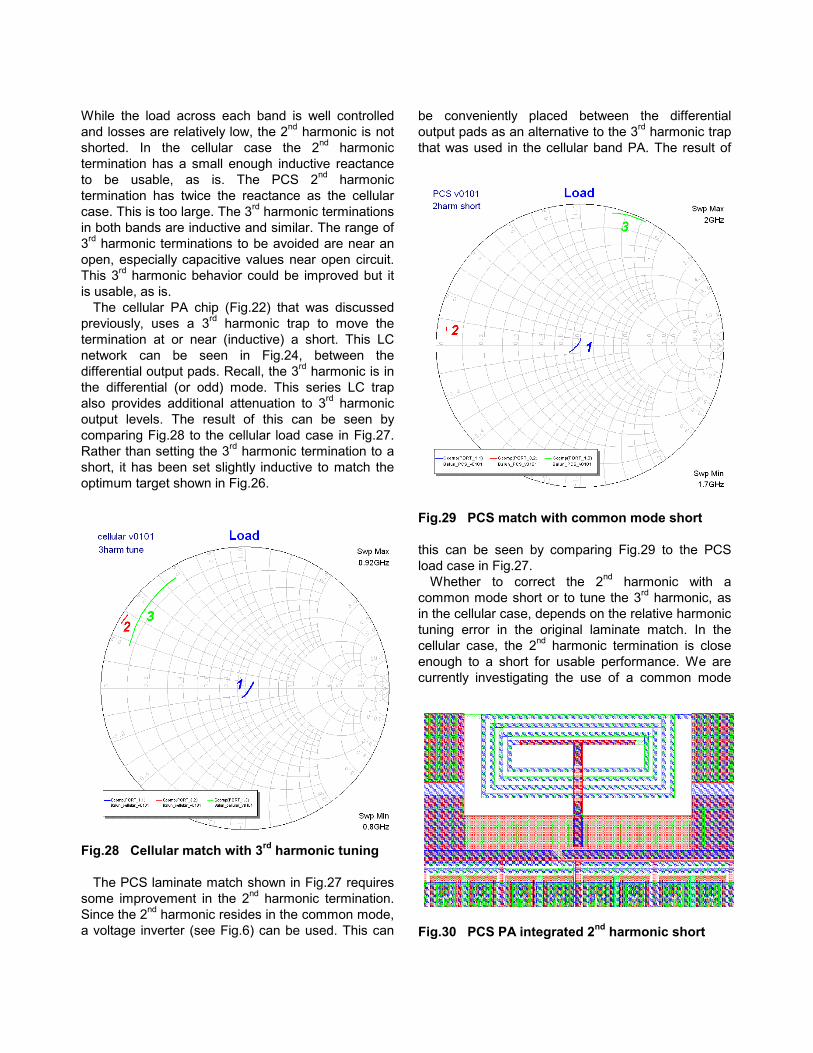
The PCS laminate match shown in Fig.27 requiressome improvement in the 2nd harmonic termination.Since the 2nd harmonic resides in the common mode,a voltage inverter (see Fig.6) can be used. This can
be conveniently placed between the differentialoutput pads as an alternative to the 3rd harmonic trapthat was used in the cellular band PA. The result of
Fig.29 PCS match with common mode short
this can be seen by comparing Fig.29 to the PCSload case in Fig.27.
Whether to correct the 2nd harmonic with acommon mode short or to tune the 3rd harmonic, asin the cellular case, depends on the relative harmonictuning error in the original laminate match. In thecellular case, the 2nd harmonic termination is closeenough to a short for usable performance. We arecurrently investigating the use of a common mode
Fig.30 PCS PA integrated 2nd harmonic short

short in the cellular case. In the PCS laminate, thereis no question that the 2nd harmonic tuning error is amuch greater issue than that of the 3rd harmonic.Fig.30 shows a voltage inverter used to provide acommon mode short in a PCS PA. The center tapnode is returned to a large bypass capacitor that isdistributed along the output cell array.
XII. LAMINATE LAYOUTS FOR PUSHPULL PAS
The cellular and PCS multimode PA module laminatelayouts (high Vcc cases) are shown in Figs.31 and32. Each design is for full bandwidth operation: 824MHz to 915 MHz cellular and 1.71 GHz to 1.98 GHzPCS. The laminates for both bands are very similar.
Fig.31 Cellular multimode pushpull PA layout
The primary difference is in the size of the outputbalun structure. These layouts embody the casesthat were discussed in the previous performancesection. Both output structures are modified Guanellatransformers stacked with choke baluns, asillustrated previously in Fig.17. Layouts were done inthe AWR environment using MAT051 PDK modifiedfor SEMCO’s 50um/50um (line width/gap) six layerrules. Both are DRC compliant. Prototypedevelopment work has been with wire bond chipsthat use substrate vias. Ultimately, production chipswill likely be done with a flip-chip interface.In addition to high Vcc operation (for buck-boost DC-DC), low Vcc operation has been explored in thecellular band. A reduced load impedance isnecessary to support the same power levels as the
Fig.32 PCS multimode pushpull PA layout
DC supply is lowered. The 9:1 auto-transformerstructure that was shown in Fig.18 was used in thelow Vcc design. Fig.33 shows a cellular layout of thistype. The cascaded choke balun can be seen in thelower left corner of the layout.
Fig.33 Cellular multimode low Vcc PA layout
It is possible to realize good performance over avery wide bandwidths with pushpull configured PAsthat operate at high supply voltage. Our firstexploratory investigation of pushpull operation was aPA that spanned 1.3 octaves from 800 MHz to 2.0GHz. This operated at a supply rail of 5.5 V. GoodWCDMA performance was seen in the two cellularand in the three PCS bands contained in that range.In general, as the transformation ratio is increased,the bandwidth performance is traded off. This is dueto the practical limitation in coupling coefficient in the

transmission line unit elements. For this reason, the1.3 octave PA was configured with a 1:1 balun. Inorder to provide full WCDMA power, 5.5 V is needed.The 1:1 balun consists of a voltage inverter cascadedwith a choke balun similar to the circuit shown inFig.10. This PA can be seen in Fig.34, as a flip chiplayout. The voltage inverter occupies the upper rightcorner while the choke balun can be seen in thelower right corner of the layout.
Fig.34 Wideband (1.3 octave) pushpull PA layout
XIII. MEASURED PERFORMANCE
Currently, the PCS amplifier shown in Fig.32 isunder development and performance data is not yetavailable. The cellular amplifiers shown in Figs. 31and 33 are more mature. For example, the high VccPA (Fig. 31) operates in GSM, EDGE, and WCDMAat supply voltages of 4.6, 3.9 and 3.5, respectively.Outstanding performance is obtained across severalcellular bands spanning the frequency range from824 MHz to 915 MHz. This multiple mode andmultiple band amplifier capability is sometimes calleda “CONVERGED PA”.
Typical power performance in GSM is better than+34.5 dBm with 63% power added efficiency (PAE).WCDMA PAE performance is typically 40% at outputlevels of +28 dBm (or greater) and -40dBc ACPR.EDGE PAE is similar to that of WCDMA at powerlevels of +28.5 dBm. The power efficiencyperformance of this amplifier in each of the modes isbetter than most single mode amplifiers. Thisapproach provides enough margin in PAE to enableuse of a Buck-Boost DC-DC converter with acompetitive overall efficiency. As was stated in theintroduction, superior PAE is a result of both the
increased load impedance from pushpull operationand of the elevated supply voltage. Both thesefactors also aid in achieving true multimode operationfrom a single PA. The simplicity of mode changes bychanging only the supply voltage is very attractive.This approach also allows a means of providing highPAE at power back-off by simply reducing the supplyvoltage. Fig.39 shows the overall PAE measured witha prototype NSC “Talon” Buck-Boost converter andour converged PA as a function of battery voltage. Itis important to note the relatively flat insensitivity inPAE. In contrast, a PA designed optimally to operateat 2.5V would be significantly challenged to do betterthan this. Another advantage available to a PA with aBuck-Boost converter is a straight forward path toload insensitivity; but, that’s a topic for another paper.
Fig.35 PAE performance in all modes
Fig.36 ACPR performance in WCDMA and EDGE

Fig.37 GSM PAE and power output vs input
Fig.38 WCDMA PAE and ACPR vs power output
Fig.39 PAE with DC-DC converter vs Vbattery
It is useful to put the performance of this PA inperspective by comparing it with our best single-ended WCDMA PA, the “plain-Jane” (Dec.2007).Fig.40 displays ACPR of both PAs vs power output atthree different DC supply voltages. The modulation inall cases is HSUPA-2.6 dB backoff. This wasselected to aggressively challenge the linearityperformance. From the -40 dBc ACPR limit, it can beseen that both amplifiers are loaded for similar powervs Vcc. At supply voltages of +3.5, +4.0, and +4.5 V,output levels of +26.5, +27.5, and +28.5 dBm areassociated with -40 dBc ACPR. From Fig.41 theimprovement in PAE in the pushpull amplifier isobserved to be approximately 5%. An increase ingain of 2.5 dB is also typical.
Fig.40 Pushpull to “plain-Jane” comparisonshows similar loading for power vs ACPR
Fig.41 Pushpull to “plain-Jane” PAE comparison

XIV. OTHER CONSIDERATIONS
Stability in general and into mismatch are importantaspects of PA design. A small signal Rollett or Linvillcheck is not sufficient to insure a stable poweramplifier. For example, if the final stage array of cellsis electrically distributed over more than a halfwavelength at frequencies where substantial gain ispresent, an odd mode (transverse direction)oscillation may be possible. This is seen occasionallyin Ku band single-ended PAs and can arise withoutlarge signal operation. So an undesired odd modeoscillation can be present in an amplifier that isintended for even mode operation. Similarly, apushpull PA may be susceptible to even modeinstability. The additional degree of freedom offeredby mode separation in a pushpull PA requires carefulattention to both modes. A linear analysis in thedifferential mode will probably not show instabilitytendencies in the common mode. A quick (but notconclusive) check of the common mode can beperformed by using voltage inverters to couple intothat mode and performing a linear stability analysis. Ifthis indicates problems, they are real. If none areapparent, some may still be hidden. The only way toinsure stability is to perform a rigorous analysis thatconsiders conditions at each active device, such asthe NDF technique of Platzker [7].
Power amplifiers are by nature nonlinear. Thebehaviors of (RF amplifier) constituent transistorsdepend on operating signal levels. Consequently,stability can be present at small signal and vanish atlarge signal. Large signal conditions change withchanges in load. Clearly, a comprehensive stabilityanalysis must consider conditions at each device (asin NDF) over a wide range of operating conditionssuch as power level and load. The best way toaddress this complicated problem is with an auxiliarygenerator technique [8].
VII. CONCLUSION
The development of pushpull power amplifiers forhandset applications has been presented. Thisapproach offers superior performance whencompared with conventional single-ended PAs.
The key element enabling these amplifiers is a lowloss, compact and inexpensive balun output circuit.
General transmission line transformer and balundevelopment was discussed. Realization in multilayerlaminate media, for output matching was detailed.Integration on chip, for input and interstage matching,was also presented.
Optimum load and source impedances forconverged PA operation were presented atfundamental, 2nd and 3rd harmonic frequencies. Thiswas provided in both PCS and in cellular bands.
Performance of laminate media output baluns wascompared to the optimum load targets. Harmoniccompensation techniques were also given.
A cellular two-stage amplifier circuit was discussedin detail with measured results.
ACKNOWLEDGEMENT
The authors wish to acknowledge the lab supportfrom T.J. Kramer, assembly support from MarshaLeanna, and layout by Eric Reavis.
REFERENCES
[1] Ruthroff, C.L., “Some Broad-Band Transformers”,Proc IRE, Vol 47, August 1959, pages 1337-1342
[2] Guanella, G., “Novel Matching Systems for HighFrequencies,” Brown-Boverie Review, Vol 31,September 1944, Pages 327-329
[3] Sevick, J., Transmission Line Transformers, 4th ed.,Noble Publishing, 2001.
[4] Gómez-Jiménez, P., Otero, P. and Márquez-Segura,E., “Analysis and design procedure of transmission-line transformers”. IEEE Transactions on MicrowaveTheory and Techniques, Vol. 56, No. 1, pp. 163-171,January 2008.
[5] Hilbers, A.H., ”On the design of HF wideband powertransformers”, Philips (Eindhoven) ElectronicApplication Laboratory Report ECO6907, 1969
[6] Speciale, R.A., “Even- and odd-mode waves fornonsymmetrical coupled lines in nonhomogeneousmedia,” IEEE Transactions on Microwave Theory andTechniques, vol. 11, pp.897-908, November 1975.
[7] Platzker, A., Struble, W. and Hetzler, K., InstabilitiesDiagnosis And The Role of K In Microwave Circuits,"IEEE MTT-S Int. Microwave Symposium Digest, 1993,pp. 1185-1188.
[8] Suarez, A., and Quere, R., “Stability analysis ofnonlinear microwave circuits,” Artech House, 2003.