Embed Size (px)
Citation preview
DESIGN DESCRIPTION: A HIGH-SPEED VARIABLE RATE PSK SATELLITE MODEM November 15, 2003
Cimarron Systems, LLC Copyright © 2003—all rights reserved.

DESIGN DESCRIPTION: A HIGH-SPEED VARIABLE RATE PSK SATELLITE MODEM
Table of Contents
List of Figures
Figure 1: Transmitter Module High-level Block Diagram. 4 ..............................................................................Figure 2: Transmit Data Spectrum—Primary Filtering. 5 .................................................................................Figure 3: Receiver Module High-level Block Diagram. 6 .................................................................................Figure 4: Receiver Module Adjacent Channel Spectral Environment. 6 ............................................................Figure 5: Optimum Receive Filter Design Minimizes ISI. 7 ..............................................................................Figure 6: Receiver FIR Digital Filter Design. 8 ...............................................................................................Figure 7: Carrier and Symbol Timing Phase Detector Implementations. 9 .........................................................Figure 8: Uncoded OM-73(V)/G Bit Error Rate Performance. 11 ......................................................................Figure 9: OM-73(V)/G Bit Error Rate Performance Using Rate 1/2 Coding. 12 ..................................................Figure 10: OM-73(V)/G Bit Error Rate Performance Using Rate 3/4 Coding. 13 ................................................
Document: DD-031115-1
Document Status: Released Revision: 1.0
Notice: The copyright in this document, which contains information of a proprietary nature, is vested in Cimarron Systems, LLC. The content of this document may not be used for purposes other than that for which it has be supplied and may not be reproduced, either wholly or in part, in any way whatsoever, nor may it be used by, or its content divulged to any other person whomsoever without prior written permission. For further information regarding this document, please contact Cimarron Systems, LLC at [email protected].
Introduction 1.............................................................................................................................Purpose and Scope 1 ...............................................................................................................References 1 ............................................................................................................................
OM-73(V)/G Modem Design 2................................................................................................System Requirements 2 ............................................................................................................Modem Implementation 3 .......................................................................................................Controller Module 3 ...............................................................................................................Transmitter Module 3 ..............................................................................................................Receiver Module 4 ..................................................................................................................Modem Performance 10 ..........................................................................................................Acquisition Performance 10 .....................................................................................................Bit Error Rate Performance 11..................................................................................................
Copyright © 2003 Cimarron Systems, LLC—all rights reserved. !i

DESIGN DESCRIPTION: A HIGH-SPEED VARIABLE RATE PSK SATELLITE MODEM
Introduction This document provides a high-level description of the design of the OM-73(V)/G satellite modem set developed by M/A-COM Linkabit, Inc. for the U.S. Army Satellite Communications Agency as part of a major upgrade of its segment of the global Defense Satellite Communications System (DSCS) satellite network.
Purpose and ScopeAlthough the described modem set began development in 1985 and was fully deployed within the DSCS network by 1990, the design description illustrates a number of important principles of the optimum communication system design methodology. For example, the use of programmable finite impulse response (FIR) filters in the receiver allows filter characteristics to the precisely matched for data rate, adjacent channel conditions, and Eb/N0. Specifically, implementation of the custom VLSI circuits that perform receive digital filtering, demodulation, and FEC decoding of the forward and reverse data channels, illustrates how this development methodology is used as the foundation in modern communication system design.
In addition, in order to further illustrate the robustness of the approach, measured performance of the modem set, both coded and un-coded, at 1.4 and 1.1 adjacent channel spacing at specified signal power and data rates, are presented and compared to ideal PSK modem performance.
Moreover, even with advances in the level of circuit component integration achievable today, most of the modem’s performance specifications are still unsurpassed. Indeed, the modem set is today a very cost-effective mainstay of the U.S. Army’s Satellite Communications Agency’s network terminal equipment inventory.
Finally, the design description consists of the following sections: this introduction with references and a section following that describes the modem design as well as its measured performance.
ReferencesListed below are the sources used and referenced in this document:
1. “OM-73(V)/G Critical Design Review”. M/A-COM Linkabit, Inc. 2. “High Level Description for the OM-73(V)/G Receive Digital CCA”. M/A-COM Linkabit, Inc. 3. “OM-73(V)/G Digital Signal Processing IC High Level Description”. M/A-COM Linkabit, Inc. 4. Ha, Tri. Digital Satellite Communications. New York, NY: McGraw-Hill, 1990. 5. Shanmugam, K. Sam. Digital and Analog Communication Systems. New York, NY: John
Wiley & Sons, 1979.
Copyright © 2003 Cimarron Systems, LLC—all rights reserved. !1
DESIGN DESCRIPTION: A HIGH-SPEED VARIABLE RATE PSK SATELLITE MODEM
OM-73(V)/G Modem DesignThe OM-73(V)/G PSK modem set implements a Frequency Division Multiple Access (FDMA) digital data
1
network for the Defense Satellite Communication System. The modem utilizes a number of unique implementation approaches that result in a design that achieves exceptional performance at relatively low power and cost levels while maintaining operational flexibility. An optimum communication system design approach was utilized in order to meet the requirement for multiple modulation schemes, variable data rates, very close channel spacing, and backward compatibility with legacy modem sets.
System RequirementsThe primary purpose of the OM-73(V)/G modem system is the replacement of the MD-1002 and KY-801
modem sets with SENU Filters in order to increase the capability of the DSCS to operate high-throughput 2
satellite data networks in an efficient, flexible, and cost-effective manner.
Critical system-level requirements for the modem set include: • Modulation – CW, BPSK, and OQPSK • Data rates – 16 kb/s to 20 Mb/s • Forward-Error-Correction – rate 1/2, 3/4, or none • Filtering – SENU or primary • Compatibility with legacy DSCS equipment • Mechanical – 19 inch rack mount unit (21 deep x 13-31/32 high) • Weight – 85 lbs/unit maximum • Reliability – 4000 hrs MTBF • Maintainability – LRU MTTR 30 minutes
System functional partitioning: • Controller
− Operator interface − Set-up and control of Tx/Rx − Fault reporting
• Transmitter − Data input/clock output − Selectable CW, BPSK, or OQPSK − Selectable rate 1/2, 3/4 FEC, or none − Selectable SENU or primary filtering − Selectable differential coding − Selectable randomizer − End-to-end test pattern − Self-test
• Receiver − Accepts IF signal with +/- 25 kHz offset
The OM-73(V)/G modem program is managed by the U.S. Army Satellite Communications Agency out of Fort 1
Monmouth, New Jersey.
SENU (Spectrum Efficient Network Unit) filtering is required for backward compatibility with existing DSCS 2
equipment.
Copyright © 2003 Cimarron Systems, LLC—all rights reserved. !2

DESIGN DESCRIPTION: A HIGH-SPEED VARIABLE RATE PSK SATELLITE MODEM
− Selectable CW, BPSK, or OQPSK − Selectable FEC rate 1/2, 3/4, or none − Selectable SENU or primary filtering − Selectable differential coding − Selectable randomizer − BER display − End-to-end test − Self-test
Modem ImplementationThe OM-73(V)/G modem implementation is partitioned within three modules: the controller that provides a user interface for configuration, status and fault monitoring; the transmitter that performs source data modulation, forward error correction (FEC), and filtering functions; and the receiver that provides receive data filtering, demodulation, and FEC decode functions as further described below.
Controller ModuleThe OM-73/(V)/G architecture provides all user interface through a Controller Module, which then commands configuration for each of up to 17 Transmitter and/or Receiver Modules in any combination. Once a Transmitter or Receiver Module has been commanded into a new configuration, the Controller Module is no longer needed; the Transmitter and Receiver Modules contain their own processors that monitor status and control all functions, including setting up all operational parameters required for the desired configuration, executing acquisition algorithms, and monitoring for any fault conditions. Thus the Transmitter and Receiver Modules are essentially standalone units needing a Controller Module only to provide an operator interface for status monitoring as required.
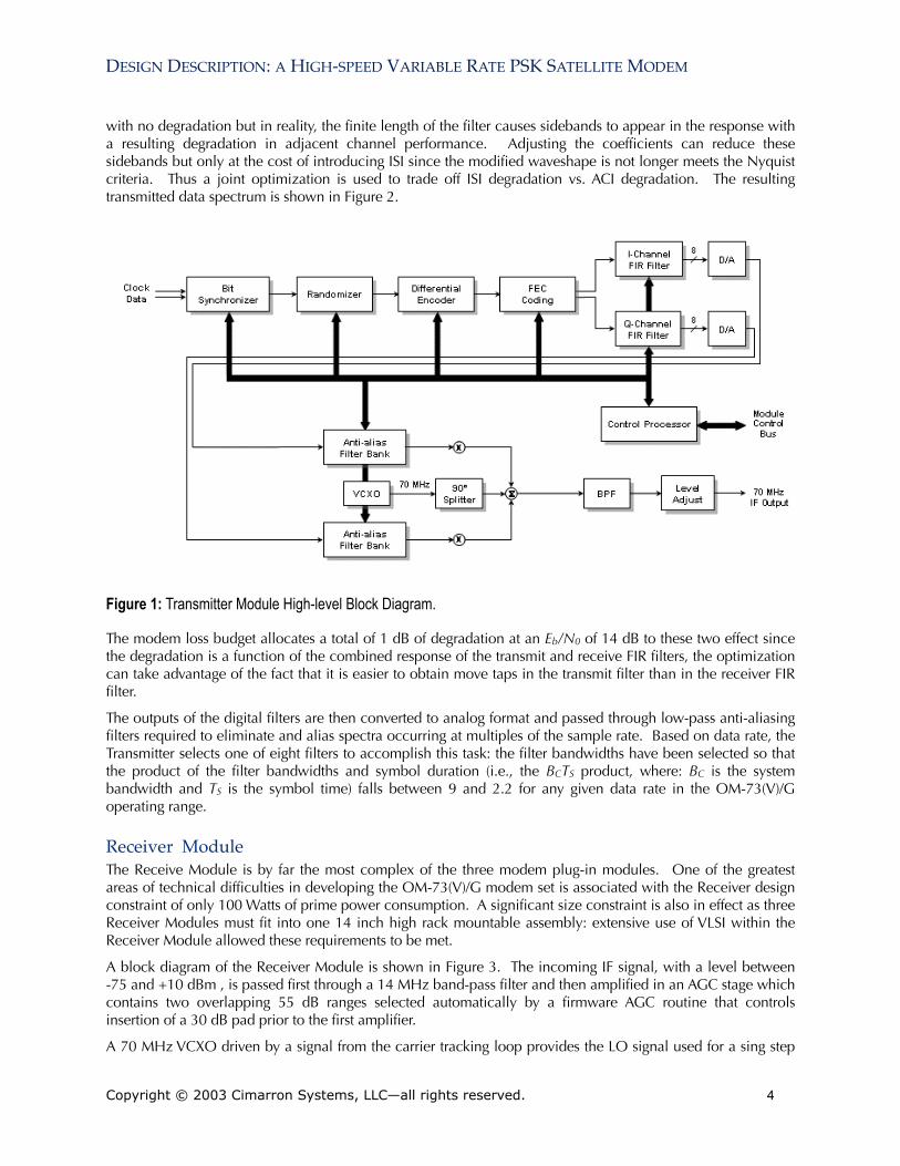
Transmitter ModuleA high-level block diagram of the Transmitter Module is shown in Figure 1. The incoming data and clock are input to the transmit bit synchronizer. The bit synchronizer is designed to have a pull-in range slightly wider than the 100 ppm accuracy with which the data rate is set by the operator meeting the requirement that the operate over a continuum of data rates from 16 kb/s to 20 Mb/s.
The synchronized data may then be randomized, if desired, to ensure an acceptable transition density, and may be differentially encoded if desired to allow the receiver to resolve phase ambiguity. Following the optional randomizer, forward error correction is applied when selected. The resulting symbols (one I data bit for BPSK operation or one I plus one Q bit for OQPSK operation) are fed to two digital filters which create four filtered output samples for each input symbol. The digital filters are implemented using Program Read Only Memory (PROM) look-up tables containing the sums of products of tap coefficients and input data samples.
Since the SENU filter has a frequency rolloff corresponding to a seven pole filter, it is fairly straightforward to represent with a 29-tap FIR digital filter with minimal resulting degradation from inter-symbol interference (ISI). Although legacy SENU filters each have individually tuned, fixed bandwidths, the OM-73(V)/G representation of these filters has a slightly different bandwidth for each data rate since it uses one set of coefficients for all of the five pole filters and a different set for all of the seven pole filters. Since the errors are small, representing the SENU filters through a construction of this type does not cause any substantial degradation even though the resulting transmitter and receiver filtering are not truly matched.
Primary filter design is a more challenging problem since, for this case, the waveshape must provide sufficient spectral containment to meet stringent adjacent channel interference (ACI) requirements. The method for developing these coefficients selects as a starting point a raised cosine shape with a rolloff factor of .18. That is, the filter response is zero beyond 1.18 times the half-bandwidth of the spectrum. In theory, if the filter implemented actually had such a spectrum, adjacent channel spacings as small as 1.18 could be employed
Copyright © 2003 Cimarron Systems, LLC—all rights reserved. !3
DESIGN DESCRIPTION: A HIGH-SPEED VARIABLE RATE PSK SATELLITE MODEM
with no degradation but in reality, the finite length of the filter causes sidebands to appear in the response with a resulting degradation in adjacent channel performance. Adjusting the coefficients can reduce these sidebands but only at the cost of introducing ISI since the modified waveshape is not longer meets the Nyquist criteria. Thus a joint optimization is used to trade off ISI degradation vs. ACI degradation. The resulting transmitted data spectrum is shown in Figure 2.
!
Figure 1: Transmitter Module High-level Block Diagram.
The modem loss budget allocates a total of 1 dB of degradation at an Eb/N0 of 14 dB to these two effect since the degradation is a function of the combined response of the transmit and receive FIR filters, the optimization can take advantage of the fact that it is easier to obtain move taps in the transmit filter than in the receiver FIR filter.
The outputs of the digital filters are then converted to analog format and passed through low-pass anti-aliasing filters required to eliminate and alias spectra occurring at multiples of the sample rate. Based on data rate, the Transmitter selects one of eight filters to accomplish this task: the filter bandwidths have been selected so that the product of the filter bandwidths and symbol duration (i.e., the BCTS product, where: BC is the system bandwidth and TS is the symbol time) falls between 9 and 2.2 for any given data rate in the OM-73(V)/G operating range.
Receiver ModuleThe Receive Module is by far the most complex of the three modem plug-in modules. One of the greatest areas of technical difficulties in developing the OM-73(V)/G modem set is associated with the Receiver design constraint of only 100 Watts of prime power consumption. A significant size constraint is also in effect as three Receiver Modules must fit into one 14 inch high rack mountable assembly: extensive use of VLSI within the Receiver Module allowed these requirements to be met.
A block diagram of the Receiver Module is shown in Figure 3. The incoming IF signal, with a level between -75 and +10 dBm , is passed first through a 14 MHz band-pass filter and then amplified in an AGC stage which contains two overlapping 55 dB ranges selected automatically by a firmware AGC routine that controls insertion of a 30 dB pad prior to the first amplifier.
A 70 MHz VCXO driven by a signal from the carrier tracking loop provides the LO signal used for a sing step
Copyright © 2003 Cimarron Systems, LLC—all rights reserved. !4

DESIGN DESCRIPTION: A HIGH-SPEED VARIABLE RATE PSK SATELLITE MODEM
down-conversion to Baseband I and Q signals. As in the Transmitter Module, two banks of anti-aliasing analog filters are used however in the Receiver Module the BCTS product of the selected filter lies between .7 and 1.7. The filters are narrower to provide greater rejection at the alias point necessary because of the potential for significant aliasing interference, and also to minimize the amount of out-of-band energy passing through the A/D converter. The A/D converter creates four samples per symbol time: thus at the highest symbol rate of 10 Msamples/s, the sample rate is 40 Msamples/s. Each bank has 8 filters covering the various frequency ranges. Bit timing is established within the demodulator circuits by appropriate adjustment of the frequency and phase of the sample clock coming from the clock synthesizer.
!
Figure 2: Transmit Data Spectrum—Primary Filtering.
Digital FilteringThe resulting I and Q samples are then fed to two parallel digital filters, which like their counterparts in the Transmitter Module. Implement the primary and SENU filter characteristics required. The particular characteristics entirely by the stored parameters in the filters, and these in turn, are controlled by the Controller Module through its control of the system configuration. The DSP VLSI IC architecture selected includes a 29-tap FIR filter with fully programmable coefficients, a post detection gain stage, a programmable digital phase detector, a programmable second order loop filter, and a programmable lock indicator. All parameters are loaded from the module microprocessor thus ensuring that the receive filter is matched to the transmit filter as a function of the system configuration.
Since the modem must perform within the adjacent channel environment shown in Figure 4, the receive FIR filters must be capable of precise spectral selectivity when adjacent channel spectrum overlap into the channel of interest. Since the FIR filters are programmable, filter characteristics that match the configuration are programmed and may be updated as system requirements change.
!
Copyright © 2003 Cimarron Systems, LLC—all rights reserved. !5

DESIGN DESCRIPTION: A HIGH-SPEED VARIABLE RATE PSK SATELLITE MODEM
Figure 3: Receiver Module High-level Block Diagram.
!
Figure 4: Receiver Module Adjacent Channel Spectral Environment. !
Copyright © 2003 Cimarron Systems, LLC—all rights reserved. !6

DESIGN DESCRIPTION: A HIGH-SPEED VARIABLE RATE PSK SATELLITE MODEM
Figure 5 is a block diagram that illustrates the optimum communication system approach to solving the problem of ISI. The figure shows that, for a linear communication channel, the transmitter and receiver transfer functions may be combined such that Z(f)= HT(f)*HR(f) so that the system impairments of ISI and noise may be treated in combination. Received symbol decision impairments due to ISI can be minimized if a Z(f) can be found that minimizes excursions of the received symbols dn beyond the symbol time TS. Shaping transmitted data with the raised-cosine characteristic, matching the receive filter with the same characteristic, and then coherently sampling the received data dn during the TS symbol period meets these requirements and will drive ISI to an acceptably small value.
Figure 5: Optimum Receive Filter Design Minimizes ISI.
Figure 6 shows a block diagram of the canonical form of the FIR digital filter and a representation of the impulse response of the 29-tap FIR receive raised-cosine matched filter (its gain as a function of normalized frequency is similar to that of the transmit filter shown in Figure 2). Since the I and Q receive matched filters are programmable via the Controller Module, filter impulse response can be tailored to account for excess ACI due close channel spacing, adjacent channels transmitting at higher data rates at high power, and other conditions.
Automatic Gain ControlThe signal used to drive the AGC circuit is derived from the outputs of the A/D converter. The primary goal of this AGC is to amplify the incoming signal as much as possible without saturating the converter. Because the signal at the A/D converter output may contain much more adjacent channel energy than desired signal energy, the desired signal may appear suppressed at the output of the digital filter, which removes the unwanted adjacent channels. A second, ‘post-detection AGC’ is thus required to scale the outputs of the digital filter by an appropriate gain since the sample magnitudes are needed for tracking loop phase error signals and for soft decision decoding.
Carrier and Sample Time TrackingThe scales outputs of the digital filters are fed to the digital tracking loop circuits, the outputs of which
!
Copyright © 2003 Cimarron Systems, LLC—all rights reserved. !7

DESIGN DESCRIPTION: A HIGH-SPEED VARIABLE RATE PSK SATELLITE MODEM
provide the VCXO control to close the carrier tracking loop and clock synthesizer control to close the bit timing loop. Two DSP ICs are used in the modem: one filters the I-channel while the other filters the Q-channel. The filtered I-channel is routed to the Q-channel DSP and vice versa thus the tracking loop sections have both I and Q-channel samples to work with. One DSP is designated to perform the sample time tracking while the other performs carrier tracking. Appropriate phase detector characteristics are loaded into the respective programmable phase detectors by the Receive Module microprocessor. Since the carrier and timing phase detectors are fully programmable, parameters optimized for the modulation type, filtering, and data rate are loaded for each system configuration.
Figure 6: Receiver FIR Digital Filter Design.
Carrier acquisition is accomplished by sweeping: sweeping is implemented by injecting a bias into the accumulator of the loop filter. The size of the bias determines the sweep rate. Thus acquisition performance is much faster than the specification requires for all but the lowest data rates where sweep rates must be slow. In addition, the acquisition algorithm first attempts a rapid sweep which will allow acquisition at higher Eb/N0 values, and only if this fails, repeats with the slowest sweep rate required for low Eb/N0 values.
For operation at the lowest data rates, sweeping alone cannot provide the desired acquisition times. For these cases, the control processor programs the phase error signal to be zero, loads the accumulator in the
Copyright © 2003 Cimarron Systems, LLC—all rights reserved. !8
DESIGN DESCRIPTION: A HIGH-SPEED VARIABLE RATE PSK SATELLITE MODEM
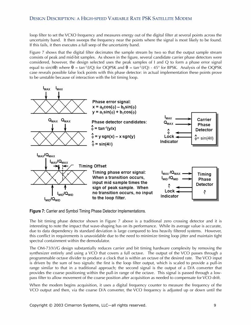
loop filter to set the VCXO frequency and measures energy out of the digital filter at several points across the uncertainty band. It then sweeps the frequency near the points where the signal is most likely to be found. If this fails, it then executes a full seep of the uncertainty band.
Figure 7 shows that the digital filter decimates the sample stream by two so that the output sample stream consists of peak and mid-bit samples. As shown in the figure, several candidate carrier phase detectors were considered, however, the design selected uses the peak samples of I and Q to form a phase error signal equal to sin(4θ) where θ = tan-1(I/Q) for OQPSK and θ = tan-1(I/Q) - 45° for BPSK. Analysis of the OQPSK case reveals possible false lock points with this phase detector: in actual implementation these points prove to be unstable because of interaction with the bit timing loop.
Figure 7: Carrier and Symbol Timing Phase Detector Implementations.
The bit timing phase detector shown in Figure 7 above is a traditional zero crossing detector and it is interesting to note the impact that wave-shaping has on its performance. While its average value is accurate, due to data dependency its standard deviation is large compared to less heavily filtered systems. However, this conflict in requirements is unavoidable due to the need to minimize timing loop jitter and maintain tight spectral containment within the demodulator.
The OM-73(V)/G design substantially reduces carrier and bit timing hardware complexity by removing the synthesizer entirely and using a VCO that covers a full octave. The output of the VCO passes through a programmable octave divider to produce a clock that is within an octave of the desired rate. The VCO input is driven by the sum of two signals: the first is the loop filter output, which is scaled to provide a pull-in range similar to that in a traditional approach; the second signal is the output of a D/A converter that provides the coarse positioning within the pull-in range of the octave. This signal is passed through a low-pass filter to allow movement of the coarse position after acquisition as needed to compensate for VCO drift.
When the modem begins acquisition, it uses a digital frequency counter to measure the frequency of the VCO output and then, via the coarse D/A converter, the VCO frequency is adjusted up or down until the
Copyright © 2003 Cimarron Systems, LLC—all rights reserved. !9

DESIGN DESCRIPTION: A HIGH-SPEED VARIABLE RATE PSK SATELLITE MODEM
desired frequency is set. At this point, the VCO is operating within the pull-in range of the loop, and the loop will be able to acquire. During tracking, the VCO is subject to drift due to temperature and voltage changes, and without attention from the microprocessor, would eventually drift beyond the hold-in range of the loop resulting in loss of lock. Thus, the processor continues to read the frequency counter and drives the coarse D/A converter so that the VCO operates well within the loop hold-in range. The bit timing loop is a modified third order construction and thus is subject to concerns about stability but, if the time constant of the processor corrections is very long with respect to the time constant of the second order loop internal, stability will generally not be a problem (as confirmed by this implementation).
Viterbi DecodingI and Q-channel filter outputs, in addition to driving the tracking loops, are also the source for the demodulator data output. To achieve the quantization required for soft decision Viterbi decoding, another gain circuit is used that maps the filter output to 3 bits. If Viterbi decoding is selected, this data is decoded, if not the sign bit of the 3-bit symbols is passed around the decoder to a differential decoder, if selected by the user, and then to a de-randomizer, if selected. At this point the data is output to the downstream terminal equipment.
The Viterbi decoder implementation in the OM-73(V)/G decodes a rate 1/2 constraint length 7 (k= 7) code or a rate 3/4 code created by puncturing the rate 1/2 code. In order to attain high data rates, a parallel computation structure is required whereby multiple Viterbi Decoder ICs are used to decode the 3-bit soft decision outputs of the I and Q-channel DSP ICs.
Modem PerformanceThe two areas of primary concerning regarding modem performance are BER and acquisition performance. The latter is of lesser concern in an FDMA system since acquisition and reacquisition are both rare events. BER performance, however, is a prime system design driver since BER performance translates directly into satellite power, FEC code rate (therefore increased bandwidth) as well as higher performing (therefore larger and more costly) uplink equipment, e.g., transmit antenna, HPA, and the like as well as downlink equipment, e.g., receive antenna, LNB, and receiver.
Acquisition PerformanceBecause of the flexibility afforded by the DSP IC design, the OM-73(V)/G is able to provide extremely fast acquisition at high data rates even for OQPSK. The maximum sweep rate that will be tolerated by a loop varies as the square of the bandwidth, and since loop bandwidth varies linearly with data rate, it is clear that with a programmable sweep rate, very fast acquisition should be obtained. In practice, it is expected that only a few seconds will be required for acquisition at rates over 1 Mb/s and most of this time will be expended performing tasks prior to sweeping that are controlled by the processor such as carrier VCXO gain characterization and bit timing VCO pre-tuning. Although the required acquisition times vary with the uncertainty range specified by the user in a linear fashion, in practice they will not follow this pattern. The main reason for this is that it is difficult to determine the precise frequency of the VCXO output without the presence of an extremely accurate standard. The OM-73(V)/G design includes a frequency counter used to measure VCXO frequency to determine its gain. This counter has a 50 ppm accuracy; thus if the actual frequency is 70.005 MHz, the measured frequency may be in error by as much as 3.5 kHz. Therefore, the modem must search a range 3.5 kHz greater than that selected to ensure that the whole uncertainty range is covered. Note that since gain is measured by taking the difference between readings at two different settings, this 3.5 kHz error is cancelled out and measured gain is accurate to within 50 ppm.
At the lowest data rates, sweep rates as low as 8 Hz/s are required. A full sweep of +/- 5 kHz would thus take 1250 seconds. To reduce this amount of time, the Receiver Module processor uses an algorithm that sweeps frequencies most likely to contain the channel center. The algorithm used to select these frequencies, called coarse frequency estimation, measures the energy at the digital filter output at increments of roughly 500 Hz. It then sweeps +/- 250 Hz around the frequency that resulted in the largest energy. If
Copyright © 2003 Cimarron Systems, LLC—all rights reserved. !10

DESIGN DESCRIPTION: A HIGH-SPEED VARIABLE RATE PSK SATELLITE MODEM
carrier lock is not found in this band, it then sweeps in the band with the next highest energy. This process continues until all bands are covered and, if lock is not achieved, the process is repeated. When the coarse frequency estimation selects the correct band, which it will do in most cases, acquisition can be expected within 100 seconds or less regardless of frequency uncertainty.
Bit Error Rate PerformanceFigure 8 shows BER performance vs. Eb/N0 for the cases for the theoretical PSK modem as well as measured OM-73(V)/G performance with adjacent channels 6 dB higher in Eb/N0 both at 1.4 and 1.1 channel spacing. Figures 9 and 10 shows measured BER performance using the Viterbi decoder with either rate 1/2 or rate 3/4, k=7 convolutional coding applied to the channel.
Figure 8: Uncoded OM-73(V)/G Bit Error Rate Performance.
Bit error rate performance close to that predicted by theory is in practice usually more difficult to achieve with increasing Eb/N0 and the OM-73(V)/G is no exception to this rule. The primary sources of degradation
!
Copyright © 2003 Cimarron Systems, LLC—all rights reserved. !11

DESIGN DESCRIPTION: A HIGH-SPEED VARIABLE RATE PSK SATELLITE MODEM
in the modem are filter inter-symbol interference, adjacent channel spectral overlap, and timing and carrier jitter. Other sources of degradation exist, these include 90 quad splitter error, I and Q Baseband gain imbalance, droop due to a DC notch filter used in the Receiver Module. Amplifier non-linearity, and modem noise figure (the latter’s effect being relatively minor).
Figure 9: OM-73(V)/G Bit Error Rate Performance Using Rate 1/2 Coding.
Tracking loops jitter causes the most degradation at the lowest Eb/N0 levels where excursions of up to 8% in either timing or carrier loops are observed. However, since performance degradation is dominated by system noise not either ACI or ISI at this operating point, these losses do not result in performance that is more than a few tenths of a dB from theory.
!
Copyright © 2003 Cimarron Systems, LLC—all rights reserved. !12

DESIGN DESCRIPTION: A HIGH-SPEED VARIABLE RATE PSK SATELLITE MODEM
For high Eb/N0 levels, the combination of ACI and ISI contribute as much a 1 dB of loss relative to theory and, for the case of 1.4 channel spacing, the degradation grows only slightly as the rate of the adjacent channel increases relative to the desired channel. This result is intuitively obvious since, when the filter rolloff is 1.18, we expect very little spectral overlap regardless of data rate.
Figure 10: OM-73(V)/G Bit Error Rate Performance Using Rate 3/4 Coding.
For a spacing of 1.1, however, modem performance is specifically affected by the relative data rate of the adjacent channel. Since the spacing is closer than the rolloff factor, spectral overlap does occur. And the amount by which the adjacent channel overlaps the desired channel is 1.18 – 1.1= .08 times the half-bandwidth of the adjacent channel. If the adjacent channel occupies 12.5 times the data rate of the desired channel, the tail of its spectrum completely overlaps the desired channel spectrum. Thus, severe degradation results when 1.1 spacing is used if channel rates are not comparable. Use of smaller rolloff factors was
Copyright © 2003 Cimarron Systems, LLC—all rights reserved. !13

DESIGN DESCRIPTION: A HIGH-SPEED VARIABLE RATE PSK SATELLITE MODEM
considered but rejected because the increased spectral steepness results in more ISI in the mid-bit samples used for bit timing with resulting in degradation in tracking performance. Under most conditions, however, spacings greater than 1.25 can be used with little additional performance loss.
For more information regarding Cimarron Systems products and services, please contact us using the contact information below.
Contact Information: Cimarron Systems, LLC Evergreen, Colorado telephone: (303) 674-9207
email: [email protected] www.cimarronsystems.com
Revision History: Date Version Notes
11/15/2003 version 1.0 Initial version.11/15/2012 version 1.1 Minor edits.
Copyright © 2003 Cimarron Systems, LLC—all rights reserved. !14