Embed Size (px)
Citation preview

R08DS0121EJ0100 Rev.1.00 Page 1 of 18 Mar 20, 2014
The mark <R> shows major revised points.
The revised points can be easily searched by copying an "<R>" in the PDF file and specifying it in the "Find what:" field.
Preliminary Data Sheet
PS9551AL4 Optically Isolated Delta-Sigma Modulator
DESCRIPTION The PS9551AL4 is an optically isolated Delta – Sigma Modulator that includes high-Accuracy A/D convertor and
converts an analog voltage input into one-bit data stream. PS9551AL4 provides Effective Number of Bit (ENOB) is 12
bits (typ) with a Sinc3 digital filter.
The PS9551AL4 is designed specifically for high common mode transient immunity (CMR) and high linearity
(nonlinearity). The PS9551AL4 is suitable for current sensing and voltage sensing in motor drives.
FEATURES • Internal Reference Voltage Tolerance (GE = ±1% MAX.)
• Effective Number of Bit (ENOB = 12 bits TYP.)
• Operating Ambient Temperature (TA = −40 to 105°C) • Non-linearity (INL = 0.14% MAX.)
• Input Offset Voltage (VOS = 3 mV MAX.)
• Input Offset Voltage Drift vs. Temperature (⏐dVos/dTA⏐ = 2 μV/°C TYP.)
• Output Clock Frequency (fCLK = 10 MHz TYP.)
• High common mode transient immunity (CMR= 15 kV/μs MIN.)
• Package: 8-pin DIP lead bending type (Gull-wing) for long creepage distance for
surface mount (L4)
• Embossed tape product: PS9551AL4-E3: 1 000 pcs/reel • Pb-Free product
• Safety standards
• UL approved: No. E72422
• CSA approved: No. CA 101391 (CA5A, CAN/CSA-C22.2 60065, 60950)
• SEMKO approved (EN 60065, EN60950)
• DIN EN 60747-5-5 (VDE 0884-5) approved (Option)
APPLICATIONS • AC Servo, inverter
• Solar inverter
• Measurement equipment
R08DS0121EJ0100Rev.1.00
Mar 20, 2014
1. VDD1
2. VIN+
3. VIN–
4. GND15. GND26. MDAT7. MCLK8. VDD2
1 2 43
6 58 7
SH
IELD
A/D Converter
Decorder
PIN CONNECTION(Top View)
<R>
PS9551AL4 Chapter Title
R08DS0121EJ0100 Rev.1.00 Page 2 of 18 Mar 20, 2014
PACKAGE DIMENSIONS (UNIT: mm)
Lead Bending Type (Gull-wing) For Long Creepage Distance For Surface Mount (L4)
9.25+0.5 –0.25
6.5+0.5–0.1
10.05±0.4
0.62±0.25
0.2±
0.15
3.7±
0.35
3.5±
0.2
1.01+0.4–0.2
2.540.5±0.15
PHOTOCOUPLER CONSTRUCTION
Parameter MIN.
Air Distance 8 mm
Outer Creepage Distance 8 mm
Isolation Distance 0.4 mm

PS9551AL4 Chapter Title
R08DS0121EJ0100 Rev.1.00 Page 3 of 18 Mar 20, 2014
MARKING EXAMPLE
R 9551ANT431
No. 1 pinMark
4 31
Year Assembled(Last 1 Digit)
TN
Rank Code
In-house Code(T: Pb-Free)
Week Assembled
Assembly Lot
Type Number
Company Initial
ORDERING INFORMATION
Part Number Order Number Solder Plating
Specification
Packing Style Safety Standard
Approval
Application Part
Number*1
PS9551AL4 PS9551AL4-AX Pb-Free Magazine case 50 pcs Standard products PS9551AL4
PS9551AL4-E3 PS9551AL4-E3-AX (Ni/Pd/Au) Embossed Tape 1 000 pcs/reel (UL, CSA, SEMKO
approved)
PS9551AL4-V PS9551AL4-V-AX Magazine case 50 pcs UL,CSA,SEMKO,
PS9551AL4-V-E3 PS9551AL4-V-E3-AX Embossed Tape 1 000 pcs/reel DIN EN 60747-5-5
(VDE 0884-5)
*1 For the application of the Safety Standard, following part number should be used.
<R>
<R>

PS9551AL4 Chapter Title
R08DS0121EJ0100 Rev.1.00 Page 4 of 18 Mar 20, 2014
ABSOLUTE MAXIMUM RATINGS (TA = 25°C, unless otherwise specified)
Parameter Symbol Ratings Unit
Operating Ambient Temperature TA −40 to +105 °C
Storage Temperature Tstg −55 to +125 °C
Supply Voltage VDD1, VDD2 0 to 5.5 V
Input Voltage VIN+, VIN− −2 to VDD1 +0.5 V
2 Seconds Transient Input Voltage VIN+, VIN− −6 to VDD1 +0.5 V
Output Voltage VOUT+, VOUT− −0.5 to VDD2 +0.5 V
Isolation Voltage*1 BV 5 000 Vr.m.s.
*1 AC voltage for 1 minute at TA = 25°C, RH = 60% between input and output.
Pins 1-4 shorted together, 5-8 shorted together.
RECOMMENDED OPERATING CONDITIONS
Parameter Symbol MIN. TYP. MAX. Unit
Operating Ambient Temperature TA −40 105 °C
Supply Voltage VDD1, VDD2 4.5 5 5.5 V
Input Voltage (Accurate and Linear) *1 VIN+, VIN− −200 200 mV
*1 Using VIN− = 0 V (to be connected to GND1) is recommended. Avoid using VIN− of 2.5 V or more, because the
internal test mode is activated when the voltage VIN− reaches more than 2.5 V.
<R>
<R>

PS9551AL4 Chapter Title
R08DS0121EJ0100 Rev.1.00 Page 5 of 18 Mar 20, 2014
ELECTRICAL CHARACTERISTICS (TYP.: TA = 25°C, VIN+ = VIN− = 0 V, VDD1 = VDD2 = 5 V, MIN., MAX.: refer to RECOMMENDED OPERATING CONDITIONS, unless otherwise specified)
Parameter Symbol Conditions MIN. TYP. MAX. Unit
Input Supply Current IDD1 VIN+ = 350 mV 12 15 mA
Output Supply Current IDD2 VIN+ = −350 mV 6 15 mA
Input Bias Current IIN −5 −0.6 5 μA
Low Level Saturated Output Voltage VOL IOUT = 1.6 mA 0.1 0.6 V
High Level Saturated Output Voltage VOH IOUT = −100 μA 3.9 4.9 V
Output Short-circuit Current |IOSC| VOUT = VDD2 or VOUT = GND2 17 40 mA
Equivalent Input Resistance RIN 450 kΩ
Output Clock Frequency fCLK 8.2 10 13.2 MHz
Isolation Resistance RI-O VI-O = 1 kVDC, TA = 25°C 1011 Ω
Isolation Capacitance CI-O f = 1 MHz 0.7 pF
Data Hold Time *1 tHDDAT 4 10 16 ns
Common Mode Transient Immunity *2 CMR VCM = 1 kV, TA = 25°C 15 kV/μs
*1 The data hold time (tHDDAT) is that the data (MDAT) will stay stable following the rising edge of the clock (MCLK).
tHDDAT is shown in the below timing chart.
Fig. Timing Chart
*2 Common Mode Transient Immunity (CMR) is specified by the rate of rise / fall of a pulse applied between GND1 on
the input side and GND2 on the output side (pins 4 and 5) by using the circuit shown in Fig. 6 CMR Test Circuit.
CMR is defined at the point that clock signals are corrupted.
MCLK
MDAT
tHDDAT
<R>
PS9551AL4 Chapter Title
R08DS0121EJ0100 Rev.1.00 Page 6 of 18 Mar 20, 2014
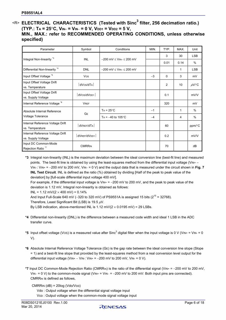
ELECTRICAL CHARACTERISTICS (Tested with Sinc3 filter, 256 decimation ratio.) (TYP.: TA = 25°C, VIN+ = VIN− = 0 V, VDD1 = VDD2 = 5 V, MIN., MAX.: refer to RECOMMENDED OPERATING CONDITIONS, unless otherwise specified)
Parameter Symbol Conditions MIN. TYP. MAX. Unit
Integral Non-linearity *3 INL −200 mV ≤ VIN+ ≤ 200 mV 3 30 LSB
0.01 0.14 %
Differential Non-linearity *4 DNL −200 mV ≤ VIN+ ≤ 200 mV 1 LSB
Input Offset Voltage *5 VOS −3 0 3 mV
Input Offset Voltage Drift
vs. Temperature ⏐dVOS/dTA⏐ 2 10 μV/°C
Input Offset Voltage Drift
vs. Supply Voltage ⏐dVOS/dVDD1⏐ 0.1 mV/V
Internal Reference Voltage *6 VREF 320 mV
Absolute Internal Reference
Voltage Tolerance GE
TA = 25°C −1 1 %
TA = −40 to 105°C −4 4 %
Internal Reference Voltage Drift
vs. Temperature ⏐dVREF/dTA⏐ 60 ppm/°C
Internal Reference Voltage Drift
vs. Supply Voltage ⏐dVREF/dVDD1⏐ 0.2 mV/V
Input DC Common-Mode
Rejection Ratio *7 CMRRIN 70 dB
*3 Integral non-linearity (INL) is the maximum deviation between the ideal conversion line (best-fit line) and measured
points. The best-fit line is obtained by using the least-squares method from the differential input voltage (VIN+ −
VIN−: VIN+ = −200 mV to 200 mV, VIN− = 0 V) and the output data that is measured under the circuit shown in Fig. 7
INL Test Circuit. INL is defined as the ratio (%) obtained by dividing [Half of the peak to peak value of the
deviation] by [full-scale differential input voltage 400 mV].
For example, if the differential input voltage is VIN+ = −200 mV to 200 mV, and the peak to peak value of the
deviation is 1.12 mV, Integral non-linearity is obtained as follows:
INL = 1.12 mV/(2 × 400 mV) = 0.14%
And Input Full-Scale 640 mV (−320 to 320 mV) of PS9551A is assigned 15 bits (215 = 32768).
Therefore, Least Significant Bit (LSB) is 19.5 μV.
By LSB indication, above-mentioned INL is 1.12 mV/(2 × 0.0195 mV) = 29 LSBs.
*4 Differential non-linearity (DNL) is the difference between a measured code width and ideal 1 LSB in the ADC
transfer curve.
*5 Input offset voltage (VOS) is a measured value after Sinc3 digital filter when the input voltage is 0 V (VIN+ = VIN- = 0
V).
*6 Absolute Internal Reference Voltage Tolerance (GE) is the gap rate between the ideal conversion line slope (Slope
= 1) and a best-fit line slope that provided by the least-squares method from a real conversion level output for the
differential input voltage (VIN+ − VIN-: VIN+ = −200 mV to 200 mV, VIN- = 0 V).
*7 Input DC Common-Mode Rejection Ratio (CMRRIN) is the ratio of the differential signal (VIN+ = −200 mV to 200 mV,
VIN− = 0 V) to the common-mode signal (VIN+ = VIN− = −200 mV to 200 mV: Both input pins are connected).
CMRRIN is defined as follows,
CMRRIN (dB) = 20log (Vdo/Vco)
Vdo : Output voltage when the differential signal voltage input
Vco : Output voltage when the common-mode signal voltage input
<R>
PS9551AL4 Chapter Title
R08DS0121EJ0100 Rev.1.00 Page 7 of 18 Mar 20, 2014
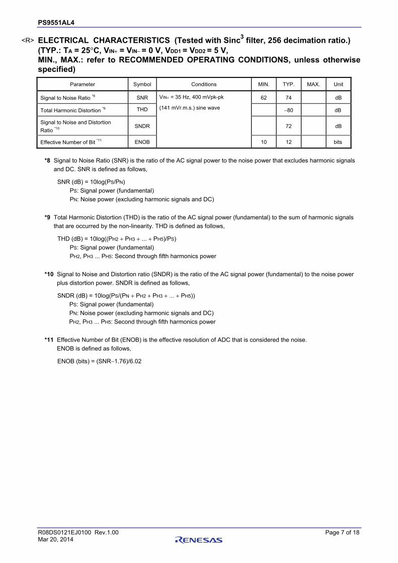
ELECTRICAL CHARACTERISTICS (Tested with Sinc3 filter, 256 decimation ratio.) (TYP.: TA = 25°C, VIN+ = VIN− = 0 V, VDD1 = VDD2 = 5 V, MIN., MAX.: refer to RECOMMENDED OPERATING CONDITIONS, unless otherwise specified)
Parameter Symbol Conditions MIN. TYP. MAX. Unit
Signal to Noise Ratio *8 SNR VIN+ = 35 Hz, 400 mVpk-pk
(141 mVr.m.s.) sine wave
62 74 dB
Total Harmonic Distortion *9 THD −80 dB
Signal to Noise and Distortion
Ratio *10 SNDR 72 dB
Effective Number of Bit *11 ENOB 10 12 bits
*8 Signal to Noise Ratio (SNR) is the ratio of the AC signal power to the noise power that excludes harmonic signals
and DC. SNR is defined as follows,
SNR (dB) = 10log(PS/PN)
PS: Signal power (fundamental)
PN: Noise power (excluding harmonic signals and DC)
*9 Total Harmonic Distortion (THD) is the ratio of the AC signal power (fundamental) to the sum of harmonic signals
that are occurred by the non-linearity. THD is defined as follows,
THD (dB) = 10log((PH2 + PH3 + ... + PH5)/PS)
PS: Signal power (fundamental)
PH2, PH3 ... PH5: Second through fifth harmonics power
*10 Signal to Noise and Distortion ratio (SNDR) is the ratio of the AC signal power (fundamental) to the noise power
plus distortion power. SNDR is defined as follows,
SNDR (dB) = 10log(PS/(PN + PH2 + PH3 + ... + PH5))
PS: Signal power (fundamental)
PN: Noise power (excluding harmonic signals and DC)
PH2, PH3 ... PH5: Second through fifth harmonics power
*11 Effective Number of Bit (ENOB) is the effective resolution of ADC that is considered the noise.
ENOB is defined as follows,
ENOB (bits) = (SNR−1.76)/6.02
<R>

PS9551AL4 Chapter Title
R08DS0121EJ0100 Rev.1.00 Page 8 of 18 Mar 20, 2014
TEST CIRCUIT
IDD1
0.01uF
IDD2
0.1uF 0.1uF
VOH
0.01uF0.1uF 0.1uF
VOL0.01uF0.1uF 0.1uF
0.01uF0.1uF 0.1uF
0.01uF0.1uF 0.1uF
IIN
VDD1
VIN+VDD2 VDD2VIN+
VDD1
VDD1
VIN+
VDD2
VDD2
VDD2
VDD1
VDD1
Fig.1 IDD1 Test Circuit Fig.2 IDD2 Test Circuit
Fig.3 IIN Test Circuit
Fig.4 Vout Test Circuit
(VOL)
(VOH)
VIN+ =-400mV
VIN+ = 400mV
<R>

PS9551AL4 Chapter Title
R08DS0121EJ0100 Rev.1.00 Page 9 of 18 Mar 20, 2014
0.01uF0.1uF 0.01uF0.1uF0.1uF IOSC 0.1uF
IOSC
0.1uF
0.1uF 0.1uF
+ -
VDD2
CLK
IN OUT
VCM
0.1uF0.1uF
VIN39
0.01uF
VDD2VDD1
SincFilter
3DATA
VDD1
VIN+
VDD2
VDD1
VDD2
78L05
9V
VIN+
Fig.5 IOSC Test Circuit
Fig.6 CMR Test Circuit
Fig.7 Vos, INL, DNL, GE, SNR, THD, SNDR, ENOB Test Circuit

PS9551AL4 Chapter Title
R08DS0121EJ0100 Rev.1.00 Page 10 of 18 Mar 20, 2014
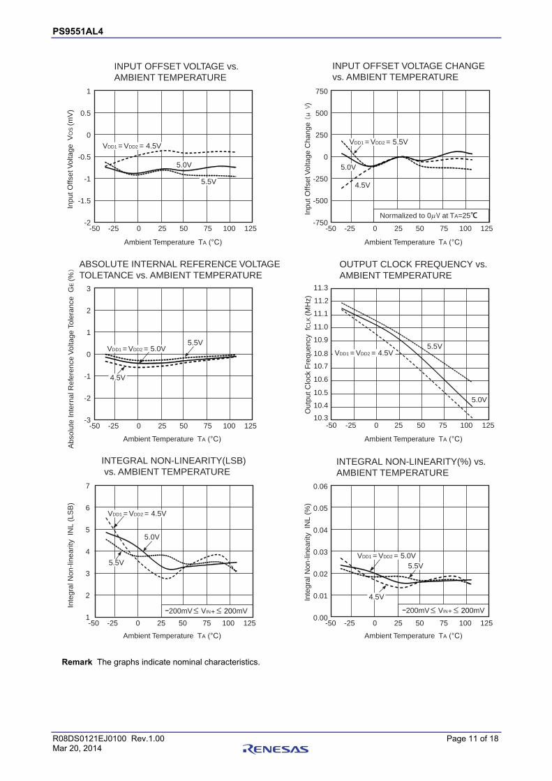
TYPICAL CHARACTERISTICS (TA = 25°C, VIN+ = VIN− = 0 V, VDD1 = VDD2 = 5 V, tested with Sinc3 filter, 256 decimation ratio, unless otherwise specified)
INPUT SUPPLY CURRENT vs. INPUT VOLTAGE
Inpu
t Sup
ply
Cur
rent
ID
D1
(mA
)
Input Voltage VIN (mV)
INPUT SUPPLY CURRENT vs. AMBIENT TEMPERATURE
Ambient Temperature TA (°C)
OUTPUT SUPPLY CURRENT vs. INPUT VOLTAGE
Inpu
t Cur
rent
IIN
(μA
)
Input Voltage VIN (mV)
Out
put S
uppl
y C
urre
nt I
DD
2 (m
A)
Out
put S
uppl
y C
urre
nt I
DD
2 (m
A)
Input Voltage VIN (mV) Ambient Temperature TA (°C)
-25 0 25 50 10075-50 125
15
9
10
11
12
13
14
-400 -200 0 200 400 -50 -25 0 25 50 75 100 125
-300 -200 -100 0 200100-400 300 400
1
-5
-4
-3
-2
-1
0
4.5V
5.0V
INPUT CURRENT vs. INPUT VOLTAGE
Input Voltage VIN (V)
Inpu
t Cur
rent
IIN
(mA)
-400 -200 0 200 400
15
9
10
11
12
13
14
9
8
7
6
5
4
9
8
7
6
5
4
2
0
-2
-4
-6
-8
-10-1 -0.5 0 0.5 1 1.5 2
VIN = -350mV
VIN = 350mV
-40°C25°C
TA = 105°C
TA = 105°C25°C
-40°C
VDD1 = VDD2 = 5.5V
VDD1 = VDD2 = 5.5V
5.0V
4.5V
INPUT CURRENT vs. INPUT VOLTAGE
Inpu
t Sup
ply
Cur
rent
ID
D1
(mA
)OUTPUT SUPPLY CURRENT vs. AMBIENT TEMPERATURE
Remark The graphs indicate nominal characteristics.
<R>
PS9551AL4 Chapter Title
R08DS0121EJ0100 Rev.1.00 Page 11 of 18 Mar 20, 2014
INPUT OFFSET VOLTAGE vs. AMBIENT TEMPERATURE
Inpu
t Offs
et V
olta
ge V
OS
(mV
)
ABSOLUTE INTERNAL REFERENCE VOLTAGE TOLETANCE vs. AMBIENT TEMPERATURE
INTEGRAL NON-LINEARITY(LSB) vs. AMBIENT TEMPERATURE
Abs
olut
e In
tern
al R
efer
ence
Vol
tage
Tol
eran
ce G
E (%)
Inpu
t Offs
et V
olta
ge C
hang
e (μV)
-25 0 25 50 10075-50 125
1
-2
-1.5
-1
-0.5
0
0.5
-25 0 25 50 10075-50 125
750
-750
-500
-250
0
250
500
-25 0 25 50 10075-50 125
3
-3
-2
-1
0
1
2
Inte
gral
Non
-line
arity
IN
L (L
SB
)
-25 0 25 50 10075-50 125
7
1
2
3
4
5
6
INTEGRAL NON-LINEARITY(%) vs. AMBIENT TEMPERATURE
Inte
gral
Non
-line
arity
IN
L (%
)
-25 0 25 50 10075-50 125
0.06
0.00
0.01
0.02
0.03
0.04
0.05
OUTPUT CLOCK FREQUENCY vs. AMBIENT TEMPERATURE
Out
put C
lock
Fre
quen
cy f
CLK
(MH
z)
-25 0 25 50 100 12575-50
11.3
10.3
10.7
10.6
10.5
10.4
10.8
10.9
11.0
11.1
11.2
INPUT OFFSET VOLTAGE CHANGE vs. AMBIENT TEMPERATURE
VDD1 = VDD2 = 4.5V
5.0V
5.5V
VDD1 = VDD2 = 5.5V
5.0V
4.5V
VDD1 = VDD2 = 5.0V5.5V
4.5V
VDD1 = VDD2 = 4.5V5.5V
5.0V
VDD1 = VDD2 = 4.5V
5.0V
5.5VVDD1 = VDD2 = 5.0V
5.5V
4.5V
Normalized to 0 V at TA=25℃
-200mV VIN+ 200mV -200mV VIN+ 200mV
Ambient Temperature TA (°C) Ambient Temperature TA (°C)
Ambient Temperature TA (°C) Ambient Temperature TA (°C)
Ambient Temperature TA (°C) Ambient Temperature TA (°C)
Remark The graphs indicate nominal characteristics.

PS9551AL4 Chapter Title
R08DS0121EJ0100 Rev.1.00 Page 12 of 18 Mar 20, 2014
SIGNAL TO NOISE AND DISTORTION RATIO vs. AMBIENT TEMPERATURE
Sig
nal t
o N
oise
and
Dis
tort
ion
Rat
io S
ND
R (
dB)
-25 0 25 50 10075-50 125
78
66
68
70
72
74
76
4.5V
5.0V
Sig
nal t
o N
oise
Rat
io S
NR
(dB)
-25 0 25 50 10075-50 125
78
66
68
70
72
74
76
5.5V4.5V
-25 0 25 50 10075-50 125
13.0
10.0
10.5
11.0
11.5
12.0
12.5
EFFECTIVE NUMBER OF BIT vs. AMBIENT TEMPERATURE
Effe
ctiv
e N
umbe
r of
Bit
EN
OB
(bi
ts)
VDD1 = VDD2 = 5.5V
VDD1 = VDD2 = 5.0V
VDD1 = VDD2 = 5.0V
5.5V4.5V
SIGNAL TO NOISE RATIO vs. AMBIENT TEMPERATURE
Ambient Temperature TA (°C) Ambient Temperature TA (°C)
Ambient Temperature TA (°C)
VIN+= 35Hz,400mV pk-pk(141mVr.m.s.) s ine wave
VIN+= 35Hz,400mV pk-pk(141mVr.m.s.) s ine wave
VIN+= 35Hz,400mV pk-pk(141mVr.m.s.) s ine wave
Remark The graphs indicate nominal characteristics.

PS9551AL4 Chapter Title
R08DS0121EJ0100 Rev.1.00 Page 13 of 18 Mar 20, 2014
TAPING SPECIFICATIONS (UNIT: mm)
330±
2.0
100±
1.0
2.0±0.513.0±0.2
R 1.021.0±0.8
2.0±0.5
21.5±1.0
17.5±1.0
PS9551AL4-E3
1.55±0.1
2.0±0.14.0±0.1 1.
75±
0.1
4.65 MAX.
9.95±0.1
12.0±0.1
1.5 +0.1–0
7.5±
0.1
10.5
5±0.
1
16.0
±0.
3
4.2±0.1
0.3±0.05
Outline and Dimensions (Tape)
Outline and Dimensions (Reel)
Tape Direction
Packing: 1 000 pcs/reel

PS9551AL4 Chapter Title
R08DS0121EJ0100 Rev.1.00 Page 14 of 18 Mar 20, 2014
RECOMMENDED MOUNT PAD DIMENSIONS (UNIT: mm)
D
CB
A
Part Number
PS9551AL4
Lead Bending A
lead bending type (Gull-wing) for surface mount
9.0
B
2.54
C
1.7
D
2.0
<R>
PS9551AL4 Chapter Title
R08DS0121EJ0100 Rev.1.00 Page 15 of 18 Mar 20, 2014
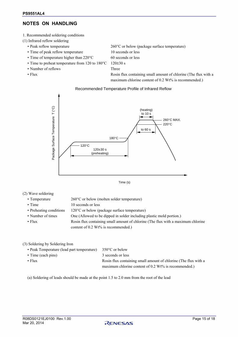
NOTES ON HANDLING 1. Recommended soldering conditions
(1) Infrared reflow soldering
• Peak reflow temperature 260°C or below (package surface temperature)
• Time of peak reflow temperature 10 seconds or less
• Time of temperature higher than 220°C 60 seconds or less
• Time to preheat temperature from 120 to 180°C 120±30 s
• Number of reflows Three
• Flux Rosin flux containing small amount of chlorine (The flux with a
maximum chlorine content of 0.2 Wt% is recommended.)
120±30 s(preheating)
220°C
180°C
Pac
kage
Sur
face
Tem
pera
ture
T (
°C)
Time (s)
Recommended Temperature Profile of Infrared Reflow
(heating)to 10 s
to 60 s
260°C MAX.
120°C
(2) Wave soldering
• Temperature 260°C or below (molten solder temperature)
• Time 10 seconds or less
• Preheating conditions 120°C or below (package surface temperature)
• Number of times One (Allowed to be dipped in solder including plastic mold portion.)
• Flux Rosin flux containing small amount of chlorine (The flux with a maximum chlorine
content of 0.2 Wt% is recommended.)
(3) Soldering by Soldering Iron
• Peak Temperature (lead part temperature) 350°C or below
• Time (each pins) 3 seconds or less
• Flux Rosin flux containing small amount of chlorine (The flux with a
maximum chlorine content of 0.2 Wt% is recommended.)
(a) Soldering of leads should be made at the point 1.5 to 2.0 mm from the root of the lead

PS9551AL4 Chapter Title
R08DS0121EJ0100 Rev.1.00 Page 16 of 18 Mar 20, 2014
(4) Cautions
• Fluxes
Avoid removing the residual flux with freon-based and chlorine-based cleaning solvent.
2. Cautions regarding noise
Be aware that when voltage is applied suddenly between the photocoupler’s input and output at startup, the output
transistor may enter the on state, even if the voltage is within the absolute maximum ratings.
USAGE CAUTIONS
1. This product is weak for static electricity by designed with high-speed integrated circuit so protect against static
electricity when handling.
2. Board designing
(1) Below figure shows a typical application circuit where the PS9551A is used. A digital filter (Sinc3 filter)
reduces high frequency quantization noise from the PS9551A and convers from one-bit data stream to 3-wire
serial data.
Fig. PS9551A Typical application circuit
(2) By-pass capacitor of more than 0.1 μF is used between VDD and GND near device. Also, ensure that the
distance between the leads of the photocoupler and capacitor is no more than 10 mm.
(3) Keep the pattern connected the input (VIN+, VIN-) and the output (MCLK, MDAT), respectively, as short as
possible. MCLK and MDAT are digital signal, but when the lines between the photocoupler and a digital filter
are long, the digital filter might not read the data.
When using long lines, use a line driver between the photocoupler and the digital filter, and keep the pattern
between the output (MCLK, MDAT) and the line driver as short as possible.
(4) Do not connect any routing to the portion of the frame exposed between the pins on the package of the
photocoupler. If connected, it will affect the photocoupler's internal voltage and the photocoupler will not
operate normally.
(5) Because the maximum frequency of the signal input to the photocoupler must be lower than the allowable
frequency band, be sure to connect an anti-aliasing filter (an RC filter with R = 39 Ω and C = 0.01 μF, for
example).
(6) When VDD is lower than 4.5 V that is the outside of recommended operating condition, the output (MCLK,
MDAT) of this product is unstable, and this might produce undesirable operation. Be sure to check the
operation of an IC that is connected to this product during Power-up and Power-down process. And we
recommend to use a disable function (shutdown function) of the connected IC or a reset IC to avoid this
undesirable operation.
3. Avoid storage at a high temperature and high humidity.
VIN+
VIN-
MCLK
MDAT
+5V
0.1uF
39
0.01uF
CLK
DAT
VDD
GND
SCLKSDATCS
VDD2
GND2
VDD1
GND1
PS9551A
+5V
0.1uF
RSHUNT
3-Wire Serial Interface
Sinc3 Filter
<R>

PS9551AL4 Chapter Title
R08DS0121EJ0100 Rev.1.00 Page 17 of 18 Mar 20, 2014
SPECIFICATION OF VDE MARKS LICENSE DOCUMENT
Parameter Symbol Spec. Unit
Climatic test class (IEC 60068-1/DIN EN 60068-1) 40/105/21
Dielectric strength maximum operating isolation voltage Test voltage (partial discharge test, procedure a for type test and random test)Upr = 1.6 × UIORM, Pd < 5 pC
UIORM
Upr
1 130
1 808
Vpeak
Vpeak
Test voltage (partial discharge test, procedure b for all devices) Upr = 1.875 × UIORM, Pd < 5 pC
Upr 2 119 Vpeak
Highest permissible overvoltage UTR 8 000 Vpeak
Degree of pollution (DIN EN 60664-1 VDE 0110 Part 1) 2
Comparative tracking index (IEC 60112/DIN EN 60112 (VDE 0303 Part 11)) CTI 175
Material group (DIN EN 60664-1 VDE 0110 Part 1) III a
Storage temperature range Tstg –55 to +125 °C
Operating temperature range TA –40 to +105 °C
Isolation resistance, minimum value VIO = 500 V dc at TA = 25°C VIO = 500 V dc at TA MAX. at least 100°C
Ris MIN. Ris MIN.
1012 1011
Ω Ω
Safety maximum ratings (maximum permissible in case of fault, see thermal derating curve) Package temperature Current (input current IF, Psi = 0) Power (output or total power dissipation) Isolation resistance VIO = 500 V dc at TA = Tsi
Tsi Isi Psi
Ris MIN.
175 400 700
109
°C mA mW
Ω
<R>

PS9551AL4 Chapter Title
R08DS0121EJ0100 Rev.1.00 Page 18 of 18 Mar 20, 2014
Caution GaAs Products This product uses gallium arsenide (GaAs). GaAs vapor and powder are hazardous to human health if inhaled or ingested, so please observe the following points.
• Follow related laws and ordinances when disposing of the product. If there are no applicable laws and/or ordinances, dispose of the product as recommended below.
1. Commission a disposal company able to (with a license to) collect, transport and dispose of materials that contain arsenic and other such industrial waste materials.
2. Exclude the product from general industrial waste and household garbage, and ensure that the product is controlled (as industrial waste subject to special control) up until final disposal.
• Do not burn, destroy, cut, crush, or chemically dissolve the product.
• Do not lick the product or in any way allow it to enter the mouth.

All trademarks and registered trademarks are the property of their respective owners.
C - 1
Revision History PS9551AL4 Data Sheet
Rev. Date
Description
Page Summary
1.00 Mar 20, 2014 Throughout Preliminary Data Sheet -> Data Sheet
Throughout Safety standards approved
p.3 Modification of MARKING EXAMPLE
Addition of ORDERING INFORMATION
p.4 Modification of ABSOLUTE MAXIMUM RATINGS
Modification of RECOMMENDED OPERATING CONDITIONS
p.5 to 7 Modification of ELECTRICAL CHARACTERISTICS
p.8 to 9 Addition of TEST CIRCUIT
p.10 to 12 Addition of TYPICAL CHARACTERISTICS
p.14 Addition of RECOMMENDED MOUNT PAD DIMENSIONS
p.16 Modification of USAGE CAUTIONS
p.17 Addition of SPECIFICATION OF VDE MARKS LICENSE DOCUMENT

http://www.renesas.comRefer to "http://www.renesas.com/" for the latest and detailed information.
SALES OFFICES
© 2014 Renesas Electronics Corporation. All rights reserved.Colophon 4.0
12F., 234 Teheran-ro, Gangnam-Ku, Seoul, 135-920, KoreaTel: +82-2-558-3737, Fax: +82-2-558-5141
Unit 906, Block B, Menara Amcorp, Amcorp Trade Centre, No. 18, Jln Persiaran Barat, 46050 Petaling Jaya, Selangor Darul Ehsan, MalaysiaTel: +60-3-7955-9390, Fax: +60-3-7955-9510
80 Bendemeer Road, Unit #06-02 Hyflux Innovation Centre, Singapore 339949Tel: +65-6213-0200, Fax: +65-6213-0300
13F, No. 363, Fu Shing North Road, Taipei 10543, TaiwanTel: +886-2-8175-9600, Fax: +886 2-8175-9670
Unit 1601-1613, 16/F., Tower 2, Grand Century Place, 193 Prince Edward Road West, Mongkok, Kowloon, Hong KongTel: +852-2265-6688, Fax: +852 2886-9022/9044
Unit 301, Tower A, Central Towers, 555 Langao Road, Putuo District, Shanghai, P. R. China 200333Tel: +86-21-2226-0888, Fax: +86-21-2226-0999
Room 1709, Quantum Plaza, No.27 ZhiChunLu Haidian District, Beijing 100191, P.R.ChinaTel: +86-10-8235-1155, Fax: +86-10-8235-7679
Arcadiastrasse 10, 40472 DTel: +49-211-6503-0, Fax: +49-211-6503-1327
üsseldorf, Germany
Dukes Meadow, Millboard Road, Bourne End, Buckinghamshire, SL8 5FH, U.KTel: +44-1628-585-100, Fax: +44-1628-585-900
Renesas Electronics Europe Limited
Renesas Electronics (China) Co., Ltd.
Renesas Electronics (Shanghai) Co., Ltd.
Renesas Electronics Europe GmbH
Renesas Electronics Taiwan Co., Ltd.
Renesas Electronics Singapore Pte. Ltd.
Renesas Electronics Hong Kong Limited
Renesas Electronics Korea Co., Ltd.
Renesas Electronics Malaysia Sdn.Bhd.
4590 Patrick Henry Drive, Santa Clara, California 95054, U.S.A.Tel: +1-408-919-2500, Fax: +1-408-988-0279
California Eastern Laboratories, Inc.
Notice1. Descriptions of circuits, software and other related information in this document are provided only to illustrate the operation of semiconductor products and application examples. You are fully responsible for
the incorporation of these circuits, software, and information in the design of your equipment. Renesas Electronics assumes no responsibility for any losses incurred by you or third parties arising from the
use of these circuits, software, or information.
2. Renesas Electronics has used reasonable care in preparing the information included in this document, but Renesas Electronics does not warrant that such information is error free. Renesas Electronics
assumes no liability whatsoever for any damages incurred by you resulting from errors in or omissions from the information included herein.
3. Renesas Electronics does not assume any liability for infringement of patents, copyrights, or other intellectual property rights of third parties by or arising from the use of Renesas Electronics products or
technical information described in this document. No license, express, implied or otherwise, is granted hereby under any patents, copyrights or other intellectual property rights of Renesas Electronics or
others.
4. You should not alter, modify, copy, or otherwise misappropriate any Renesas Electronics product, whether in whole or in part. Renesas Electronics assumes no responsibility for any losses incurred by you or
third parties arising from such alteration, modification, copy or otherwise misappropriation of Renesas Electronics product.
5. Renesas Electronics products are classified according to the following two quality grades: "Standard" and "High Quality". The recommended applications for each Renesas Electronics product depends on
the product's quality grade, as indicated below.
"Standard": Computers; office equipment; communications equipment; test and measurement equipment; audio and visual equipment; home electronic appliances; machine tools; personal electronic
equipment; and industrial robots etc.
"High Quality": Transportation equipment (automobiles, trains, ships, etc.); traffic control systems; anti-disaster systems; anti-crime systems; and safety equipment etc.
Renesas Electronics products are neither intended nor authorized for use in products or systems that may pose a direct threat to human life or bodily injury (artificial life support devices or systems, surgical
implantations etc.), or may cause serious property damages (nuclear reactor control systems, military equipment etc.). You must check the quality grade of each Renesas Electronics product before using it
in a particular application. You may not use any Renesas Electronics product for any application for which it is not intended. Renesas Electronics shall not be in any way liable for any damages or losses
incurred by you or third parties arising from the use of any Renesas Electronics product for which the product is not intended by Renesas Electronics.
6. You should use the Renesas Electronics products described in this document within the range specified by Renesas Electronics, especially with respect to the maximum rating, operating supply voltage
range, movement power voltage range, heat radiation characteristics, installation and other product characteristics. Renesas Electronics shall have no liability for malfunctions or damages arising out of the
use of Renesas Electronics products beyond such specified ranges.
7. Although Renesas Electronics endeavors to improve the quality and reliability of its products, semiconductor products have specific characteristics such as the occurrence of failure at a certain rate and
malfunctions under certain use conditions. Further, Renesas Electronics products are not subject to radiation resistance design. Please be sure to implement safety measures to guard them against the
possibility of physical injury, and injury or damage caused by fire in the event of the failure of a Renesas Electronics product, such as safety design for hardware and software including but not limited to
redundancy, fire control and malfunction prevention, appropriate treatment for aging degradation or any other appropriate measures. Because the evaluation of microcomputer software alone is very difficult,
please evaluate the safety of the final products or systems manufactured by you.
8. Please contact a Renesas Electronics sales office for details as to environmental matters such as the environmental compatibility of each Renesas Electronics product. Please use Renesas Electronics
products in compliance with all applicable laws and regulations that regulate the inclusion or use of controlled substances, including without limitation, the EU RoHS Directive. Renesas Electronics assumes
no liability for damages or losses occurring as a result of your noncompliance with applicable laws and regulations.
9. Renesas Electronics products and technology may not be used for or incorporated into any products or systems whose manufacture, use, or sale is prohibited under any applicable domestic or foreign laws or
regulations. You should not use Renesas Electronics products or technology described in this document for any purpose relating to military applications or use by the military, including but not limited to the
development of weapons of mass destruction. When exporting the Renesas Electronics products or technology described in this document, you should comply with the applicable export control laws and
regulations and follow the procedures required by such laws and regulations.
10. It is the responsibility of the buyer or distributor of Renesas Electronics products, who distributes, disposes of, or otherwise places the product with a third party, to notify such third party in advance of the
contents and conditions set forth in this document, Renesas Electronics assumes no responsibility for any losses incurred by you or third parties as a result of unauthorized use of Renesas Electronics
products.
11. This document may not be reproduced or duplicated in any form, in whole or in part, without prior written consent of Renesas Electronics.
12. Please contact a Renesas Electronics sales office if you have any questions regarding the information contained in this document or Renesas Electronics products, or if you have any other inquiries.
(Note 1) "Renesas Electronics" as used in this document means Renesas Electronics Corporation and also includes its majority-owned subsidiaries.
(Note 2) "Renesas Electronics product(s)" means any product developed or manufactured by or for Renesas Electronics.