Embed Size (px)
Citation preview
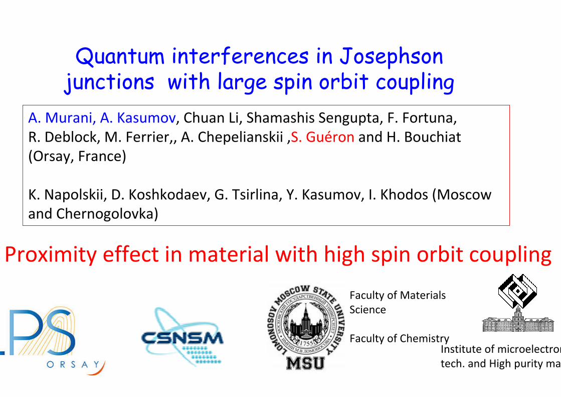
Quantum interferences in Josephsonjunctions with large spin orbit coupling
Faculty of Materials Science
Faculty of ChemistryInstitute of microelectronitech. and High purity mat.
A. Murani, A. Kasumov, Chuan Li, Shamashis Sengupta, F. Fortuna, R. Deblock, M. Ferrier,, A. Chepelianskii ,S. Guéron and H. Bouchiat(Orsay, France)
K. Napolskii, D. Koshkodaev, G. Tsirlina, Y. Kasumov, I. Khodos (Moscow and Chernogolovka)
Proximity effect in material with high spin orbit coupling

Physique mésoscopique LPS Orsay
SS
Ph
ysiq
ue
més
osc
op
iqu
eLP
S O
rsay
1 µm
S
S
S SS
300 nm
S
Guessing game… What’s what?
The proximity effect reveals spin dynamics, intrinsic pairing, atomic orbitals, dephasing, interference, band struc

Spin orbit coupling
Spin orbit interactions couple spin and spatial degrees of freedom
Spin Split bands

Spin orbit coupling
Depends on the Crystal symmetry:
Possibility to create a topological insulator
In 2D:
Hasan Kane RMP (2011)2D conducting surface states
Formation of 1D
counter propagating
spin polarised edge states
Protected from disorder
Spin orbit interactions couple spin and spatial degrees of freedom

5
Backward scattering ( 2) vorbiddenPerfect Andreev reflection (3)
Enhanced Andreev reflection
Spin split Andreev statesJosephson junctions in Zeeman field
Possibility of mixed singlet triplet correlations…
Edge states: inhomogeneous current distribution
What happens with superconducting electrodes?
Ez =ESO /2ESO = EF /2

Bismuth nanowires
Bulk, surface, edge states
Josephson effect :
• High critical current: ballistic transport ?• Field resistant induced superconductivity:• Explanation via orbital and spin effects, and topological
edge channels?• Investigation of the Andreev spectrum
6

7
Hofmann 2006 review
A semi-metal, with n ≈ 3x1017 cm-3 , m* ≈ 0.03me and λF ≈50 nm
Bulk Brillouin zone
Bulk Bi
Centrosymmetric: Bulk SO averages to 0

8
Spin split states at Bi surfaces(111) (100)
All surfaces are different, but ESO ~ EF ~ 100 meVDominate transport for this layers or wires d < 90nm
ARPES (Hoffman 2004)
calc
ula
tion
geff: 1~ 100
EFESO

Edge states on certain surfaces
9
Bi(111) bilayer Topological 2D insulator
Murakami 2006
ARPES Takayama et al PRL 2
Edge states but possibly not topological
15 nm
What about thicker layers?

10
STM on Bi(111) bilayer small pit: 1D edge states at some edges
(Drozdov Yazdani, 2014)
Bismuth edge states on (111) surface
Conclusion: confined Bi 3D semi metal 2D metal 1D edges

11
Bi nanowires
o probably facetted, with severorientations
o Practically monocrystalline (nohigh angle boundary)
o Protected by membrane residues
Electrochemically grown in 90 nm-wide pores of polycarbonate membrane.
TEM image of similar wires grown in nanopores (G. Tsirlina)
No possible caracterisation of a selected wire for transport measurements

Bi nanowires grown with sputtering
12(F. Brisset ICMMO, Anil Murani
Orientation of Bi nanowire facets Can be characterisedBy e diffraction
Pd contacts
Kasumov 2015

13
25 micron-long
Two segments with (111) facets
cleaved
uncleaved
Give different magnetoresistances!

14
Superconducting contacts by focused ion beam-assisted deposition
C and Ga-doped amorphous W wire, roughly 200 nm thick and wide, with greatsuperconducting properties:
c~4K, ∆~0.8 meV, Hc~12 Tesla!
BiW W
W(CO)6 nozzle
Ga+ beam
Kasumov 2005, Guillamon 2008
Electrodeposited
Grown with sputtering

15
High critical current at zero field , much higher than for Ag nanowires
Nearly perfect Andrev reflection in spite of interface barriers
Bi1 Bi2
N 1 kΩ 10 kΩ 16 kΩ
1,8 μA 140 nA 70 nA
Length 1.9 μm 2 μm 1.6 μm
Bi1
Supercurrent in W/Bi/W junctions
RNIC ~ 0.8 meV ~ ∆W
EJ = IcΦΦΦΦ0/2ππππ is about 1K
RNIC ~ 1-2 meV~ ∆W: maximum critical current possible for s
SNS junction !
200 mK
Bi4Bi3
1,2 kΩ
750 nA
1.4 μm

16
Back to S/Bi/S: Supercurrent persists to huge ⊥ field!
16
14
12
10
8
6
4
2
-100 -50 0 50 100IDC(nA)
0T 0.5T
1T 1.5T
2T 2.5T
3T 3.5T
4T 4.5T
5T 5.5T
6T 6.5T
7T 7.5T
8T 8.5T
9T 9.5T
10T
0 T
10 T
T = 600mK
10 T corresponds to 1000 Φ0 in the 100 nm x 2 µm wire!
Diffusive multichannel model doesn’t work. Field dependence implies: few ballistic channels!

Bi nanowires Ag nanowire
Very different behavior
0.15 T
RNIc ~ 0.15 ∆
H (T)
H (T)
Bi1
H (T)
Bi2
Bi4I (
µA
)H (T)
H (T)

Small period field oscillations of the switching current
Oscillations visible up to 7 T!
Diffusive multichannel model doesn’t work. Field dependence implies: few ballistic channels!

19
Cuevas, Montambaux
~ Gaussian decay of Ic on scale of Φ0
because dephasing by field
Diffusive trajectories encircle different fluso pick up different phases
Narrow diffusive sample with many channels: Flux dependent phase variation in sample

20
Role of geometry demonstated in SNS junctions
Exp: Chiodi 2012Theory: Bergeret Cuevas 2008
Ic decays on scale of Φ0 through sample surface(100 G)
wid
e
narrow
Narrow: L>>W
wide: L< W

SNS squid junction
21
0 30 60 90
0
30
60
B(G)
Ic(µ
A)
Fil longI
1,8µµµµm
Nb
Au
Angers 2008
Φ0 through Au wire
Φ0 through loop
B
Modulation period a few G, decay scale ~50 G

22
Back to S/Bi/S: Supercurrent persists up to huge field!
Field dependence implies: very few ballistic 1D channels!
10 T corresponds to 1000 Φ0 in the 100 nm x 2 µm wire!
Incompatible with many diffusive channels.
θij constant
Then no decay of Ic

23
SQUID-like IC oscillations, up to 10 T !
2.01.9 6.9 B(T)
60
50
40
Bi3
Bi12.0
1.5
1.0
0.5
0.054321B(T)
100mK700mK1.2K1.7K
80
75
70
210B(T)
0.80.7B(T)
70 IDC(n
A) Where is the loop?
Why no extinctionon the scale of 1 Φ0 /S ~400 Gauss?
Period 154 Gauss
Amplitude modulation0.25 T
Fourier transform Bi3

1D edge states on (111) facet (or other topological facet).
similar to observations in SC top. Insulators HgTe /HgCd Te, InAs/GaSb
Decay scale gives extension of edge state (nm!)
Other surface or bulk states will not contribute at such high fields
SQUID-like IC oscillations, up to 10 T : Very few ballisnarrow 1D channels
Bi3
Bi180
75
70
210B(T)
Bi1 Bi3
ΔB = 754G
S = 0.027 µm2
=13nm x 2 μmΔB = 154G
S = 0.13 µm2
=65nm x 2µm
Period consistent with facet size
Bi3
(

High field range modulation seen for all wires
-0.4 -0.2 0.0 0.2 0.4
IDC(uA)
p1
p2
p3
p4
4
2
0dV
/dI(
kΩ
)
-0.4 0.0 0.4IDC(µΑ)
4
2
0dV
/dI(
kΩ
)
4
2
0dV
/dI(
kΩ
)
4
2
0dV
/dI(
kΩ
)
p1
p2
p3
p4Bi2
Slow phase modulation by Zeeman energy
Critical current is larger in 5T than in zero field!

26
SOC
k
E B
SOC
k
E
High field scale critical current modulation due to Zeeman dephasing
µm vF = 3x10⁵ and geff = 30 yields period in Tesla range
Balistic 1D channel with SOC
∆k = EZ / h vF = geff µB B / hvF
δφ = 2π L ∆k = 2 geff µB B L / vF

SQUID-like IC oscillations, and high field modulation reproduced with 2 channels
Bi3
Bi180
75
70
210B(T)
Bi3
Ici(H)=Ici (1- αi cos geffi.H)
Ic1=30 Ic2, geff2=20 geff1
ZeemanΦ0
Mironov et al.PRL 2015
Squid formula with field modulated Ici : Ic²=Ic1(H)²+Ic2(H)²+2.Ic1Ic2 cos2πΦ/Φ

28
Rapid squid like oscillations (due to orbital phase modulation), and absence of decay with field: Small number of narrow (<1nm) 1D ballistic (helical) edge states.
1 Tesla range modulation explained by Zeeman (spin) dephasing
High critical current due to suppressed normal backscattering at helical edges?
Next: Investigation of Andreev states
Conclusion: what we found in S/Bi nanowire/S junctions

NS Ring periodicity h/2eN Ring periodicity h/e
From single electron spectrum in a ring to Andreev states in a long SNS junction L >> ξS
Büttiker Klapwijck 1985

Flux dependent spectrum of a ring in the presence of spin orbit coup
Phase shiftedand States
± ksoL
MultichannelNS ring Andrev states invariant by T
Andreev states are spin splitfor φ ≠ 0,πTRS breaking δE= λ∆2τD
decreased effective disorder
1D N ring
With Rashba SO couplingλ= ESO/EF=0.3
No SO coupling
How to detect level crossings at 0 and π ?
δE
(A.Murani A.Chepelianskii
H.B. Similations of BdG equ.)

Dc Josephson current
in (ϕ)= ∂ εn(ϕ)/ ∂ ϕ
Φext=Φdc+Φac cos Finite frequency response
Very sensitive to Andreev level crossings at 0 and π
(ϕ)= ∑fn(ϕ) in (ϕ)
S N
without Rashba SO
with Rahba SO
Au diffusive wire
Finite frequency

after 1 month at room T…
Regions where Ic=0 And R > RN
RN = 30kΩ
Large Field modulations of Ic, depend on the direction of magnetic field

Zeeman e/h phase shift along a ballistic channel of length L
kF + δkF
kF - δkF
δkF = EZ / h vF = geff µB B / vF
e
h
δφ = 2π L δkF = 2 geff µB B L / vF ~ π for 1T
F = 105 m/s geff =10 L=2µm
Large field modulations of Ic can be explained!Full modulation in the single channel limit
Large field modulations of the Supercurrent
B//HR

34
Current-phase relation ?
be measured in asymmetric squid configuration
SIS tunnel junctionR300K=900Ω(to be replaced by Bi nanowire)
FIB tungsten constriction weak link
=400Ω
R. Delagrange, A. Murani, R. Deblock, A. Kasumov 2014
I C(μ
A)
Φeff/Φ0
Preliminary experiment

Bi3 Shapiro steps ν=2.2 GHz

Understanding contribution of spin orbit, superconductivity, disorder, number of channels
36
Tight binding modelSquare or hexagonal lattice (H. Bouchiat, A. Chepelianskii, A. Murani, M. FerrieAdjust disorder, spin-orbit strength, junction length, …

Spectre sans spin-orbite
S,∆, −ϕ/2
S, ϕ/2Normal metal wire: Au, Cu,
Ag
ϕϕ
Eg~3.1 ETh
Spectre normal sans spin -orbite
Spectre avec contacts supra(sans spin-orbite)
H. Bouchiat, M. Ferrier

Spectre normal (anneau): effet du spin-orbite
Pas de spin-orbiteEtats dégénérés en spinCroisements évités (couplage par désordre)
Faible spin-orbite Fort spin-orbite
- Dégénérescence de Kramers, à phase nulle.-« Splitting » de spin-Certains croisement autorisés : « disparition du désordre »
Φ
H. Bouchiat, A. Chepelianskii, A. Murani

SNS Junction
Lambda3splitting
N ring
N seul, Pas de spin-orbiteEtats dégénérés en spinCroisements évités (couplage par désordre)
Φ ϕ=2πΦ/Φ0
SNS, Pas de spin-orbite- Etats dégénérés en spin- Gap induit, ne se ferme pas à π
SNS, avec spin-orbite-Kramers ,-levée de la dégénérescence de s-Gap induit se ferme à π: disparition du désordre! (certain
λ=3
S,−ϕ/2
S, ϕ/2
Spin-orbitedésordre
Chepelianskii, A. Murani, HB

Peu de canaux de conduction, courant critique oscille, ne décroit pas avant 50 quanta de fl
Et montrer manips Geim
Alexei Chepelianskii: test non extinction du courant critique à fort champ
Beaucoup de canaux de conduction, courant critique décroit à qq quanta, mais petit courant critique subsiste jusqu’àbeaucoup plus fort champ
Ballistique, 10 canaux
Exp S/ballistic Graphene/S, Geim, Avril 2015

Properties of FIB deposited « tungsten » nanowires
Auger analysis :tungsten10 % carbon10 % Ga5% oxygen
TC = 4-5 K, HC = 12 T (pure W has Tc of less than 100 mK !)Length = several microns, typical width = 100 nm to 500nm
Very reproducible superconducting parametersNice electrodes for investigation of proximity effect…
S (WFIB)
N(Au)
S (WFIB)1 µm
Kasumov et al; 2005

42
-20
00
20
0
-80 -70 -60 -50Idc(nA)
H = 0
Open questions…
junction SQUID?
2 different samples which have Icoscillations show always minimum at zero field.

43
Similar to proximity effect in Quantum Spin Hall EffectHgTe/HgCdTe quantum wells, Yacoby Molenkamp, 2014
Vg=1.05V trivial transport, uniform supercurrent density
Vg=-0.425V, supercurrent flows via helical edges states!

Shubnikov de Haas oscillations seen at T>Tc
44
T=6K

• SdH oscillations with 1/2-shifted behavior (i.e. γ=1/2): Diracelectrons on the surface
45
Dirac-type surface states on Bi nanoribbons
Ning et al. (2014) arXiv:1404.5702:
(110), 50 nm thick

Proximity effect
46
NS
L<min(Lφ,LT)
S
Andreev reflection
e h
Constructive interferences
Time reversal symmetry
Proximity effect is a very sensitive probe of coherence, spin properties in different systems

47
4. Bi thin film and surface structure
I. Introduction - Bismuth
Long de Broglie wavelength ~120ÅSemimetal – semiconductor transition at a critical thickness: 320Å
C.A. Hoffman PRB (1993)
Truncated-bulk for (100)
Mönig PRB 72 (2005) 085410
Truncated-bulk for (111) Truncated-bulk for (110)

What do you get with Bi nanowires?
Proof: Aharonov-Bohm oscillations in parallel field (Nikolaeva 2008)
B
α = 0°
Bi
55 nm
Clear period: as if cylinders are hollow: only surfaces?48

Oscillatory decay for a planar SIS or wide SNS junction
49Fraunhoffer pattern for a wide junction
S
L<<W
S
θN
Flux dependent phase variation at boundary θ(y)