Embed Size (px)
Citation preview

Protection and Fusing in Advanced
Automotive Electrical Environmentby
lija Jergovid
Submitted to the Department of Electrical Engineering and ComputerScience and Department of Physics in partial fulfillment of the
requirements for the degrees of
Bachelor of Science in Physics
and Bachelor of Science in Electrical Science and Engineering
and Master of Engineering in Electrical Engineering and ComputerScience
at the MASSACHUSETTS INSTITUTE OF TECHNOLOGY
September 1999
@ Massachusetts Institute of Technology 1999. All rights reserved
Signature of Author
Certified by
Accepted by
Accepted by
Departmefit of Elefrical Engiering and Computer Sciencee c E / September 9,1999
'K Professor John G. Kassakian-N Thesis Supervisor
Prolessor Arthur SmithChair, Department Committee on Graduate Thesis
Department of Electrical Engineering and Computer Science
Professor David E. PritchardSenior Thesis Coordinator, Department pLPhvsics
I I I I - I

2

Protection and Fusing in Advanced
Automotive Electrical Environmentby
Ilija Jergovid
Submitted to the Department of Electrical Engineering and Computer Science
and Department of Physics in partial fulfillment of the requirements for the
degrees of
Bachelor of Science in Physics
and Bachelor of Science in Electrical Science and Engineering
and Master of Engineering in Electrical Engineering and Computer Science.
AbstractProtection and fusing is a highly important subsystem in an automotive
electrical distribution system (EDS). As a result of increased power demand anew 42 V EDS is introduced in the automotive industry. This thesis investigatesthe impact of voltage change on various types of protection devices such asconventional fuses (CF's), smart power switches (SPS's) and polymeric positivetemperature coefficient devices (PPTC's).
In Chapter 2 an overview of the theory of operation of these devices ispresented and is then followed by the different means of characterizations andcomparison which is given in Chapter 3. Many of these means of characterizationare in widespread use for CF in the industry today and their applicability on otherdevice types is discussed. Furthermore, some new means of characterization arepresented as a result of added functionality of PPTC's and SPS's. Chapter 4presents the comparison of the three device types on the basis of theorypresented in Chapter 2 and means of characterization presented in Chapter 3.Where possible the performance changes due to source voltage increase areevaluated and compared among different devices. Chapter 5 deals with elementsof circuit and system protection closely related to the automotive EDS. Examplesof analysis include cable protection and protection coordination.
These analyses reveal that, excluding economic issues, the bestperforming protection device in many cases is the SPS. However, wheninductance is present in the faults the fuses can 'handle' higher inductancevalues during fault interruption.
Thesis Supervisor: John G. KassakianSupervisor's Title: Professor of Electrical Engineering
3

4

AcknowledgmentsDuring the course of my academic study at MIT I have never crossed the
30 page boundary of the academic term paper. As I began to write this thesis Inever believed that it would be so much different to produce a 100 pagedocument. Fortunately, the help of many people around me made the processsubstantially easier.
The precious guidance of Dr. Tom Keim has earned him my highestgratitude and respect. Both during the research and the writing of this thesis heevaluated and guided my work in the most professional way. Even at momentswhen I lost track of my thoughts he was there to help me determine the rightdirection for this thesis. My Advisor, Prof. John Kassakian, has always found timeto help me with my research in spite of his numerous other obligations. Duringthe early stages of the research he helped me define the research unit and thescope of the research. While it seemed initially impossible to find the appropriatedirection the advice and conversations between Prof. Kassakian and me definedthe research presented in this thesis.
Since this research was done under the sponsorship of the AutomotiveConsortium, numerous persons in the industry have helped me define the currentstatus of the protection and fusing and identify the elements interesting to myresearch. Most of the subcommittee members have in some way supported myresearch effort. Alfons Graf and Tom Tobin from Infineon Technologies havegiven me both the resources and the technical help necessary to betterunderstand their technology. Furthermore, although Raychem is not a member ofthe Consortium I would like to thank all the application engineers at Raychem fortheir help in trying to characterize polymeric positive temperature coefficientprotection devices.
Finally I would like to thank my friends Milos Komarcevic, Edo MacanKatja Djepina for many hours of support they have given me throughout the lastyear. While the morning coffee was one of the most important elements ofsupport, many hours of phone conversations with Mi have proven to be anexcellent source of inspiration. Furthermore, I would like to thank the lastelements of public sanity in Croatia, Radio 101 and Feral Tribune. Knowing thatthey still exist gives me hope that some day I might return.
5

6

Table of Contents
1. INTRODUCTION ................................................................................................................... 15
1.1. HISTORY AND DESCRIPTION OF THE PROBLEM ................................................................... 15
1.2. O BJECTIVE .......................................................................................................................... 17
1.3. O RGANIZATION OF THE THESIS .......................................................................................... 17
2. THEORY OF DEVICE OPERATION................................................................................. 19
2.1. INTRODUCTION .................................................................................................................... 19
2.2. CONVENTIONAL FUSES ..................................................................................................... 20
2.2.1. Pre-arcing behavior of CF's ................................................................................. 21
2.2.2. Arcing behavior of CF's ........................................................................................ 25
2.3. SMART POW ER SW ITCHES ............................................................................................... 30
2.3.1. Fuse function of the SPS ...................................................................................... 33
2.3.2. Turnoff of an Inductive load ................................................................................. 35
2.3.3. Added functionality ............................................................................................... 37
2.4. POLYMERIC POSITIVE TEMPERATURE COEFFICIENT DEVICES............................................... 38
2.4.1. M icroscopic behavior........................................................................................... 38
2.4.2. M acroscopic behavior........................................................................................... 41
2.4.3. Inductive fault interruption.................................................................................... 45
3. CHARACTERIZATION OF DEVICES............................................................................... 47
3.1. INTRODUCTION .................................................................................................................... 47
3.2. M EANS OF CHARACTERIZATIONS CURRENTLY IN USE........................................................... 47
3.2.1. Definitions ................................................................................................................. 47
3.2.2. f"t value.....................................................................................................................49
3.2.3. Current versus tim e plot....................................................................................... 50
3.2.4. Therm al derating coefficient and curves............................................................... 52
3.2.5. Safe operating voltage (Voltage rating)............................................................... 53
3.2.6. Maxim um fusing current (Breaking capacity test) .................................................... 54
3.2.7. Cut-off characteristic............................................................................................. 54
3.3. NEW MEANS OF CHARACTERIZATION ................................................................................. 55
3.3.1. Resetability ............................................................................................................... 55
3.3.2. M odes of Failure.................................................................................................... 56
7

3.3.3. Maximum load inductance during operation and fault conditions ........... 57
3.3.4. Post trip current ................................................. ................................................. 58
4. THEORETICAL AND EXPERIMENTAL COMPARISON OF PROTECTION DEVICES...59
4 .1. INTRO D UCTIO N .................................................................................................................... 59
4.2. 42 V FAULTS COMPARED TO 14 V FAULTS ........................................................................ 60
4.3. VARIATIONS IN I-T PLOTS OF PROTECTION DEVICES DUE TO VARIOUS EFFECTS AT CONSTANT
AM BIENT TEM PERATURE ................................................................................................................ 60
4.4. VARIATIONS IN I-T PLOTS DUE TO CHANGES IN AMBIENT TEMPERATURE...................................66
4.5. COMPARISON OF PERFORMANCE DURING TURNOFF OF FAULT CURRENTS IN CIRCUITS WITH
INDUCTIVE LO ADS ............................................................................................................ ........ 72
4.6. COMPARISON OF POWER DISSIPATION OF PROTECTION DEVICES IN NORMAL MODE OF
O P E RAT IO N .................................................................................................................................. 8 0
4.7. POST-TRIP CURRENT FOR RESETABLE DEVICES ................................................................ 86
5. CIRCUIT AND SYSTEM FUSING AND PROTECTION ................................................. 95
5 .1. INTRO D UCTIO N .................................................................................................................... 95
5.2. PROTECTION OF CABLES ..................................................................................................95
5.2.1. Cable and Protection at same Tamb .-............................................ 96
5.2.2. Cable and Protection at different Tamb .........-----...- ............................... 97
5.2.3. Self inductance of the cable .................................................................................. 99
5.3. PARALLEL CONNECTION OF PROTECTION DEVICES...............................................................102
5.4. CURRENT LIMITED POWER SUPPLY .................................................................................... 104
5.5. PROTECTION COORDINATION ............................................................................................. 111
5.5.1. Coordination of the -t curves ................................................................................. 113
6. CONCLUSION .......... ......... .....- - ... -....--..... ... 119
6 .1. C O NC LUS IO NS ................................................................................................................... 119
6.2. RECOMMENDATIONS FOR FUTURE STUDIES ......................................................................... 121
REFERENCES.........................................................................................................123
BIBLIOGRAPHY...................................................................................................125
APPENDIX A ...................................................................................................... 129
APPENDIX B...........................................................................................................133
8

List of Figures page
Figure 2.1 Steady state fuse link temperature as a function of current for ahypothetical fuse composed of Zn....................................... 23
Figure 2.2 A plot of time to melt as a result of applied current for ahypothetical Fuse composed of Zn........................................23
Figure 2.3 Equivalent circuit for a fault at the formation of gaps..................26Figure 2.4 Current through a fuse and voltage across the fuse during
a rcing .......................................................................... . .. 2 8Figure 2.5 Block diagram of the SPS with sense function..........................30Figure 2.6 I-V characteristic of a power mosfet for two different values of
gate voltage and the resulting characteristic of the BTS 660 Ptype S P S ..................................................................... . . 3 1
Figure 2.7 I-V characteristic of BTS660P as a function of temperature (11).Reprinted with perm ission. ................................................ 32
Figure 2.8 Time to switch off for a BTS 410 E2.(Inductive turnoff notincluded) (11). Reprinted with permission. ............................. 33
Figure 2.9 Circuit applicable during an inductive load turnoff with an SPS.(Rc=RL+RESR)- . -.. - - - - - - - - - - - --.................................................36
Figure 2.10 Logarithmic plot of energy imparted on the SPS during aninductive load turnoff as a function of initial turnoff current Iand inductance present in the circuit. (The horizontal surfaceis the m axim um allowed). .................................................. 36
Figure 2.11 The equivalent resistance of two resistors connected inparallel when the resistance of one resistor is kept constant atR=500 Q and the resistance of the other is varied. .................. 39
Figure 2.12 Specific volume of HDPE as a function of temperature (17).Reprinted with perm ission. ................................................ 40
Figure 2.13 Resistance of PPTC as a function of temperature (11).Reprinted with perm ission ................................................. 41
Figure 3.1 l-t plot for a BTS 640 S2 showing /mfc and /om for a leftmostcurve. Variations due to different heat sinking strategy (11).Reprinted with perm ission. ................................................ 51
Figure 3.2 l-t plots of Raychem's RXE product family of PPTC's (19).Reprinted with permission. ................................................ 52
Figure 3.3 Temperature derating factors for three device types..................53Figure 3.4 Cutoff characteristic of the BTS 650 P type SPS. The higher
curve obtains for the device turned on at the moment the faultoccu rs.......................................................................... . . 56
Figure 4.1 /-t plot for a ATO blade fuse with /nom=1OA .............................. 61Figure 4.2 Variations in I-t plots as a result of variations in fuse production
process for an ATO 1 OA fuse ............................................. 63Figure 4.3 Dependence of production parameters such as Ron and Isep on
SPS I-t curve (11). Reprinted with permission......................... 64
9

Figure 4.4 Hold and Trip characteristic for RUE 400 PPTC device atTamb= 2 50C ........................................................................... 6 6
Figure 4.5 Temperature variations in the /-t characteristics for an ATO 10Afuse ............................................................................. . . 6 7
Figure 4.6 Effect of the ambient temperature change on the I-tcharacteristic of a 20A MAXI fuse ........................................ 68
Figure 4.7 Worst case dependence of /-t plot for the SPS accounting for allparameter variations and temperature operating range (11).Reprinted with perm ission. ................................................ 69
Figure 4.8 I-t characteristic of a RGE500 type PPTC for high currents,obtained by experiment at Raychem..................................... 71
Figure 4.9 Interpolated time to trip as a function of ambient temperature at/p=30A for a RGE500 type PPTC. Shown are the maximum,m inim um and typical times ................................................. 71
Figure 4.10 Effect of arcing 2t on the ATO 10A fuse performance .............. 73Figure 4.11 Arcing 12t for an ATO 10A fuse when T is kept constant ............ 74Figure 4.12 Maximum allowable time constant as a function of /p for an
ATO 1OA fuse ................................................................. 75Figure 4.13 Inductance limitation for an ATO 10A fuse under the constant
T limitation given by the manufacturer.................................... 76Figure 4.14 Virtual arcing time as a function of prospective current for a
BTS 550 P assuming Vs=13V and Emax=1.2J.........................77Figure 4.15 Allowed values of resistance R. and inductance L. in any
mode of operation for a BTS 650P type SPS ........................ 78Figure 4.16 Inductance limitation as a function of circuit resistance for BTS
410 E2 type SPS. Results for two source voltages are shown........79Figure 4.17 Power dissipation of the fuse as a function of nominal rated
current. Results shown are for Littelfuse 32 V ATO typestandard fuses and Pudenz 58 V FKS type fuses. ................... 81
Figure 4.18 Power dissipation as a function of minimum fusing current forBTS 640 S2 type SPS. Minimum fusing current changed byaddition of heat sink. Smallest value represents no heat sink.......83
Figure 4.19 Comparison of minimum power dissipation as a function onImfc for SPS's produced by Infineon and conventional fuses.Parts rated to operate in both 42V and 14 V systems areshow n ......................................................................... . . 84
Figure 4.20 Experimentally determined power dissipation of PPTC prior totripping and after at least one trip as a function of hold current.PPTC's rated for both 42 V and !4 V systems are shown.Power dissipation of fuses is plotted for comparison. ............... 85
Figure 4.21 Experimentally recorded SPS current during the interruption ofthe fault current. Data shown is for BTS 640 S2 type SPSproduced by Infineon.......................................................... 86
Figure 4.22 Blowup of the experimentally determined waveform shown inFigure 4.21 after thermal steady state is reached. ................... 87
10

Figure 4.23 Computed theoretical steady state RMS value of post faultcurrent for the BTS 640 S2 type SPS as a function ofprospective current. Results computed assume the sourcevoltage of 12.6 V .............................................................. 88
Figure 4.24 Experimentally determined values of the steady state RMSvalue of post-trip current superimposed with the theoreticallypredicted results shown in Figure 4.23. Device under test wasthe BTS 640 S2 type SPS. ................................................ 89
Figure 4.25 Transient behavior of the period by period RMS value of thepost-trip current for the BTS 640 S2 type SPS........................90
Figure 4.26 Theoretically computed post-trip current in the tripped state asa function of prospective current and two source voltages for aRUE900 type PPTC.......................................................... 91
Figure 4.27 Post-trip current in the tripped state as a function of sourcevoltage for lp=30 A for a RXE375 type PPTC..........................92
Figure 4.28 Experimentally determined steady state value of post-tripcurrent superimposed with the theoretical predictions. Thedevice under test was the RUE900 type PPTC. ...................... 92
Figure 5.1 I-t characteristic for cables of different cross sectional area andPV C insulation ................................................................. . 96
Figure 5.2 Dependence of the short circuit time (Lc/Rc) constant as afunction of cable radius . Length of the cable is kept fixed at 5m ..................................................................................... 1 0 0
Figure 5.3 The time constant of the fault as a function of prospectivecurrent. The fault is considered to be generated by shorting ofth e ca b le ............................................................................ 10 1
Figure 5.4 The effect of change in thermal resistance of the device on theBTS 550 P 1-t characteristic.(Reprinted by permission ofInfineon technologies)..........................................................103
Figure 5.5 I-V Characteristic of a CLPS superimposed by a resistive loadline. Current lim it is roughly 100 A .......................................... 104
Figure 5.6 Load lines of three device types superimposed onto the I-Vcharacteristic of a C LPS ....................................................... 106
Figure 5.7 I-V characteristic of the CLPS and a BTS 640 S2 as the faultresistance changes (increasing values of Re are indicated bythe direction of the arrow ).....................................................107
Figure 5.8 Trajectories of the operating point in I-V space during a faultprotected by a SPS for a CLPS with the indicated steady statecha racte ristic ..................................................................... 108
Figure 5.9 Equivalent series resistance of the 13 V automotive battery asa function of state of charge .................................................. 109
Figure 5.10 Steady state I-V characteristic of the current limited powersupply together with the battery of low state of charge................110
Figure 5.11 Tree structure of the coordinated automotive protectionsystems. The order of protection devices is shown.....................111
Figure 5.12 Protection coordination of two loads with different criticality.......113
11

Figure 5.13 Coordination of the first order SPS and a conventional fusedemonstrating the constant time perceived by the high orderfu s e ................................................................................. 1 1 5
Figure 5.14 Hypothetical situation in which an SPS fails to coordinate witha low order fuse in the occurrence of the fault...........................116
12

List of Commonly used Symbols
a Linear temperature resistance coefficient.Cp Isobaric specific heat capacity.Emax Maximum energy allowed to be dissipated in the smart power
switch during turnoff.F Minimum fusing factor, ratio of /mfc and Inom./mfc Minimum fusing current. Smallest current necessary for the device
to begin turnoff.ft Integral of the square of the current up to some time t. For example,
melting ft would be integrated up to onset of melting from thebeginning of a fault.
/P Prospective current.limit Current limit of the current limited power supply./Scp Maximum actual current that can exist in an SPS during a fault.
Current limit of the associated MOSFET./0 Magnitude of current at the onset of turnoff./trip Largest value of /mfc.'hold Smallest value of /mfc-/nom Nominal current.'load Current supplied to a load or a group of loads in normal conditions.'post Post trip current for resetable devices./-t Usually designating a plot of prospective current vs. virtual time.Lc Inductance present in the circuit.Pd Power dissipation.Rth Thermal resistance of the SPS.RESR Equivalent series resistance of the sourceRo Nominal resistance of a protection device at ambient temperature.R, Resistance of the fuse.Rc Resistance present in the circuit excluding the resistance of the
protection device.Tmelt Melting temperature.Tamb Ambient Temperature.Timax Maximum temperature of the silicon junction of the SPS. When this
temperature is reached turnoff is initiated.T Temperature of the SPS junction.tmelt Time to melt.T Circuit time constant (Lo/ R).U Heat loss coefficient (to the environment).Vs Voltage of the source.VDS Drain to source voltage of the SPS.VC, Voltage at which SPS starts conducting to protect it self from
overvoltage.VL VCr VSVmax Maximum allowed operating voltage for a protection device
13

14

Chapter 1.
Introduction
1.1. History and Description of the Problem
The history of the automotive electrical system clearly reveals the
increasing power demand presented to the electrical distribution system. Since
power is the product of current and voltage the magnitude of the current present
throughout the system is always increasing. Historically, one of the solutions to
these increasing power needs was the industry's switch from the old 6V
automotive electrical system to the new 12V automotive electrical system. The
short term effect of this switch was the reduction in system current by a factor of
two. The long term effect were the thirty years in which the 12V electrical system
managed to meet the power demands of the automotive environment in an
economically feasible way . However, due to the ever increasing power demand
in the modern luxury vehicle, the automotive manufacturers have come to the
conclusion that the current 12V volt system will need to be changed in order to
meet the power demands of the future in the most feasible economical way. The
need for a new electrical distribution system (EDS) is visible in the increasing
15

size of the alternators and batteries. Some luxury cars today even have two
alternators and two batteries in order to meet their power demands
One of the initial steps in the specification of the new electrical system
was the formation of the MIT/Industry Consortium on Advanced Automotive
Electrical/Electronic Components and Systems (1). One of the tasks of the
consortium was to determine the appropriate new voltage for the automotive
electrical distribution system. The principal tradeoffs were a desire for increased
power capability, driving towards higher voltages, and retaining touch safety,
which posed an upper limit. These matters were considered by consortium
member companies, both in the context of the consortium, and along with other
interested parties, in a German-based ad hoc organization called Forum
Bordnetz. The voltage chosen was 42V. This represents a three-fold increase in
the system voltage. Today 42V volts is an agreed standard by the industry for the
nominal voltage of the future automotive EDS.
Unfortunately, economic and technical considerations do not allow an
easy transition to a new 42 V system and the abandonment of the old 12V
system. Thus came the idea of a hybrid 12V-42V dual voltage system. The
development of this dual voltage system is at a stage where the architecture of
the final electrical distribution system is not yet clearly defined but the candidate
architectures are being examined within the work of the consortium.
One of the issues in the development of this new dual voltage system is
the fusing and protection issue. In order to protect the electrical distribution
system from various types of failures car manufacturers use electric fuses and
other protection devices (2,3). Today's automotive fuses are not capable of
operating at 42V. The nonexistence of such a fuse does not imply that it is not
being developed. In fact its development is underway. Since there was no need
for the automotive fuses rated to safely operate in the new 42V system they did
not exist. As the need is becoming more and more apparent the fuses are
starting to appear in the market.
However, new advanced technologies have been developed that have the
potential to replace the conventional fuse because of the increased functionality
16

that they can offer. The transitory period now existing in the automotive industry
is one of the most convenient times for introduction of these new technologies
and the reevaluation of the currently used technologies and protection strategies.
1.2. Objective
The purpose of this thesis is to evaluate conventional fuses and new
technologies and compare them on both theoretical and experimental basis.
Furthermore, identification and exploration of the circuit and system issues of the
current and probable future fusing and protection strategies are important for the
transition period since they will uncover existing problems and predict future
problems. With respect to the future automotive electrical distribution system this
thesis is set out to compare the impact of the future candidate architecture on the
protection and fusing issues and strategies. The new fusing and protection
devices need to be characterized effectively in the view of the current fusing and
protection standards of operation and characterization.
1.3. Organization of the thesis
Chapter 2 presents the theory of operation for conventional fuses (CF),
smart power switches (SPS), and polymeric positive temperature coefficient
devices (PPTC).
In Chapter 3 different means of device characterization are established and
then used to evaluate the performance of different device types on theoretical
and experimental basis in Chapter 4.
Chapter 5 investigates various applications of three protection device types
and makes a comparison of their performance. The applications include the
protection of cables, use of devices in parallel connection, use of devices on a
current limited power supply system and their use in a protection coordinated
environment.
Finally Chapter 6 contains the conclusions and recommendations for
future studies.
17

18

Chapter 2.
Theory of Device Operation
2.1. Introduction
In order to evaluate the feasibility of devices for use as protection devices in
current automotive electrical distribution system and future dual voltage electrical
distribution systems it is necessary to have a comprehensive understanding of
the principles of device operation and the underlying physical laws that govern
the operation.
The theory of device operation gives the first basis for comparing different
device types. It also enables the prediction of behavior of the device only on
theoretical basis and is a starting point in the development of simulation models
used during the design of the systems. This predictive power of the theory proves
to be a major contribution to assessing the usability of different device types in
current and future automotive electrical environments.
Furthermore, if we choose to neglect the underlying principles of operation
we could easily neglect some factor and thus degrade the reliability of the overall
system (e.g. nuisance fuse blowing - a fuse that operates even though its
19

minimum fusing current is never exceeded). Thus, oversimplification of the theory
of device operation is both detrimental and dangerous.
The theory that follows does not only give the underlying physical principles
but also facilitates the optimization of protection for systems to be performed to
the best of one's ability and provides the system with protection that best suits
the needs of that particular system. The theory of conventional fuse operation will
be presented first. Although well known, CF theory of operation offers significant
advantage to understanding the theory of operation of both SPS and PPTC
devices. Furthermore, some of the aspects of the theory of CF operation are
often given little attention during the system design today as they have not
caused any problems yet (e.g. Inductance limitations). However, some of these
aspects might become more and more important as the new 42 V electrical
distribution system is introduced. The smart power switch (SPS) and polymeric
positive temperature coefficient device (PPTC) theory of operation follows.
22. Conventional Fuses
All conventional fuses operate on the same underlying principle. They pass
electrical current through a fusible link. When the current exceeds a certain value
the energy dissipated in the fusible link is large enough to cause the vaporization
and melting of the link. The physical behavior of the CF while the current passes
through the material from which the fusible link is composed is termed pre-arcing
behavior. After the fusible link has melted and the passage of current is not
through any phase of the link material arcing will begin. The physical principles of
arcing are termed arcing behavior.
Under normal operating conditions the CF operates in the pre-arcing
regime. During the interruption of excessive currents both the pre-arcing and the
arcing regime are present. Only in an idealized, inductance-free environment
there would be no arcing present. Due to the presence of parasitic inductances
the arcing regime is always present. Behavior of the fuse in the arcing regime
defines many of the characteristics of the fuse.
20

2.2.1. Pre-arcing behavior of CF's
The pre-arcing behavior of the conventional fuse can further be divided
into three distinct regimes of operation. These three regimes are governed by the
amount of current that is passing through a fuse. The behavior of the fuse link in
all three regimes can be simply described by a following differential equation:
mcdT =1 R - U(T - Tamb)( dt
where m is the total mass of the fuse link, c, is the specific heat capacity of the
material that the fuse link is composed of, T is the temperature of the fuse link in
C, Tamb is the ambient temperature in 0C, / is the current passing through the
fuse link, R is the resistance of the fuse link, and U is the heat loss (to the
surrounding) coefficient. The resistance has additional temperature dependence
given by:
R =Ramb +a(T-mb)] (2.2)
where Ramb is the resistance at Tamb=25 1C and ais the linear resistance
temperature coefficient. In order to separate various regions of operation, the
melting temperature for the fusible link material Tmeit needs to be known. Just
looking at Equation 2.1 it can be seen that the left hand side is zero under the
steady state condition. In this situation the following equation holds:
/2R = U(TTamb) (2.3)
meaning that for a given current I the fuse link will reach some temperature T.
The electrical energy dissipated in the fuse link is lost to the environment. A
simple reasoning deduces that if the T reached is above the melting temperature
of the fusible link Tmeit the situation is not physically acceptable since the fusible
link has already melted. Thus the first region of operation is the operation under
which the steady state current does not cause the melting of the fusible link. This
21

is the normal operating regime of the system. The fuse can pass some maximum
current called minimum fusing current /mfc for an infinite duration without
beginning to melt.
On the other hand, if the fuse is passing a current greater than /mfc the
fuse link will begin to melt. The time it takes the fuse link to begin melting is
determined by integrating Equation 2.1 until T reaches TweIt. This defines the
second regime of operation.
As the current is further increased the times required for melting to begin
become shorter and shorter. At some point the times are so short that all of the
electrical energy dissipated in the fuse link is used to heat the fuse link and none
is lost to the environment. For this regime of operation, the environment loss
coefficient is set to zero reducing the differential equation to:
mcP dTj =12 R (2.4)(dt
This regime of operation is called the constant 12t regime or, somewhat
ambiguously, adiabatic regime, to indicate that the energy supplied to the fusible
link is entirely used to heat the fuse link and there is no exchange of heat with the
environment (however energy is supplied to the fusible link). This is the third
regime of operation of the CF during the pre-arcing period of the fuse operation.
In order to obtain theoretical results from the above mentioned equations,
it is necessary to define all the constants appearing in Equation 2.1 and 2.2. The
results examined in this chapter were created by using a square geometry of the
fusible link composed of Zinc (Zn). The exact dimensions and values of all the
constants related to this hypothetical fuse are not important for our discussion
and can be found in the Appendix A along with the more detailed treatment of
Equation 2.1.
Two different kinds of results were obtained using the above mentioned
model for the hypothetical fuse given in Appendix A. For the normal regime of
operation (regime N - for normal) the temperature of the fuse link for a given
amount of current was be determined. This is visible in the Figure 2.1.
22

500
450
400
350
(D 300-
250-
.200 -Ep* 150'
100~
50
0 10 20 30 40 50 60 70Current [1]
Figure 2.1 Steady state fuse link temperature asa function of current for a hypothetical fusecomposed of Zn
If the current exceeds the minimum fusing current the time to melt as a
function of current can be calculated. Figure 2.2 depicts this time to melt and the
other two regimes of operation. The boundary between normal regime of
operation and the regime in which heat exchange with the environment still
happens (regime E- exchange regime) is clearly defined as the minimum fusing
current /mfc. However, the boundary between the regime E and the adiabatic
10 3 -Regime E
CD Regime NCO
E.0
0)2E 10
Regime A,
ld 102Current [1]
Figure 2.2 A plot of time to melt as a result ofapplied current for a hypothetical fusecomposed of Zn.
23

regime (regime A) is not sharp. As the current levels are increased regime E
slowly transits into regime A. Operation in regime N is shown in Figure 2.1.
Figure 2.2 shows the three regimes of operation.
The 12t line (dashed line) is the line for which U was set to zero and one
can see that the fuse characteristic approaches this line asymptotically as I gets
large. Thus the transition from regime E to regime A is not sharp, but a slow
function of increasing fault current.
However, in this model some simplifying assumptions were made. It was
assumed that the current density in the fusible link is constant. It was also
assumed that the temperature is the same throughout the fusible link.
Furthermore, it was assumed that the fusible link is composed of only one type of
metal.
These assumptions do create a certain amount of errors in our model. The
first two assumptions are very important because they apply to any type of
fusible link. In order to investigate the effect of these assumptions the fusible link
has to be divided into a large number of pieces and Equation 2.1 needs to be
applied for each individual piece. Furthermore, the exchange of heat between
pieces has to be accounted for in U. Further investigation of these refinements
can be found in literature (4,5).
The third assumption directly influences the operation in the normal
operating regime and deserves discussion. A. W. Metcalf discovered an effect
first called 'M' effect (4) and now called diffusion pill technology (6). If the fusible
link is coated with solder the interruption of the fuse happens faster since the
fusible link acts at lower temperatures than the melting temperature of the fusible
link material. The melting temperature of solder is lower than that of the fusible
link material and thus it melts before the fuse link does. After the solder is in the
liquid state the fuse link material (e.g. Zn) starts to dissolve into the solder and
causes the fusible link to break faster due to the formation of solder-zinc alloy
which has a lower melting point than zinc.
Unfortunately, if the system design engineer is not aware of the existence
of this type of technology in the fuse link he could cause the diffusion process to
24

begin even at some current in the normal operating regime thus causing the fuse
to nuisance blow. Therefore there is a current for which the fuse performance
begins to deteriorate. In our theoretical fuse this would be 48.2 A if a solder
globule composed of material conforming to the DIN standard L-Sn60Pb was
used. The melting temperature of this type of solder is 1850C . This is visible in
the Figure 2.1 in which one sees that for 48.2 A passing through the fuse the
temperature of the fusible link reaches 1850C. Therefore, although the fuse might
continue to operate after its temperature exceeds 1850C the diffusion process
has begun and is irreversible. Reducing the current below 48.2 A before the fuse
blows leaves one with a faster acting fuse in case of a subsequent fault current
appearance. Furthermore, after such an irreversible heating event, the minimum
fusing current Imfc of the fuse might be altered, and typically it is reduced.
To summarize, pre-arcing behavior of the fuse link is divided into three
different regimes of operation. In the normal region the fuse never blows because
the fuse link never melts. However, its performance can deteriorate if its
temperature exceeds some specified value (temperature at which the diffusion
pill begins to melt). If /mfc(Tamb) is exceeded the fuse will melt and the only
question is how fast. Under a high fault current regime, 12t is constant which
enables determination of this time. At lower fault currents energy exchange with
the environment is present and must be accounted for resulting in higher times
than a constant 12t would predict. The minimum fusing current /mfc is defined as
the current for which this melting time approaches infinity. All aspects of the pre-
arcing behavior are strictly current dependent and are not influenced by the
system voltage. The system voltage becomes important in considerations of the
arcing behavior.
2.2.2. Arcing behavior of CF's
As the fuse begins to melt some of the fusible link material is present in the
liquid phase. If the liquid phase is electrically in parallel with the solid phase the
heating is concentrated in the solid phase as a result of its lower resistance. Due
to this higher power dissipation, all of the electrically parallel solid phase
25

eventually transitions into liquid phase. Now, the liquid phase is in series with the
lower resistance solid phase resulting in higher heat dissipation in the liquid
phase and subsequent vaporization of some percentage of the liquid phase.
Both the vapor and the melted phase are free to move resulting in formation
of gaps. These gaps initially act as capacitors. If the inductance of the circuit
could be zero the current would be interrupted. However due to presence of
inductance in the circuit the current can not go to zero instantaneously. Due to
the low initial capacitance of the gaps they charge rapidly till the breakdown
electric field of the gap is reached. At this time the arcs are formed.
Lc
Vcap Cgap
VS
R =Rf+RcFigure 2.3 Equivalent circuit for a fault at theformation of gaps
Figure 2.3 is the equivalent circuit that represents the above situation. Here
Lc is the inductance of the circuit, and V, is the source voltage. R is the total
resistance of the circuit composed of the resistance of the fuse element RF and
any additional resistance Rc present in the circuit. As the fuse begins to melt Rf
increases even further since the liquid phase has higher resistivity and the linear
dependence (Equation 2.2) does not hold any more. During the pre-arcing period
Cgap can be taken to be infinity. At the moment the gaps are formed Cgap reduces
to a rather low value. This causes a fast increase of the voltage drop across the
fuse. When Vcap exceeds the breakdown voltage, arcing commences and
persists until the current goes to zero.
26

The discussion of arc behavior in the next several paragraphs is drawn from
Wright and Newbery (4). It is provided here as a convenience to the reader.
The arc is separated into three distinct regions. The first region is the anode
fall region, the second region is the cathode fall region, and the connecting
region is the positive column. Vaporized fuse link material ionizes and acts as a
conductor in the arc (4).
The anode fall region is 10-3mm long. Voltage drop across the region is
taken to be roughly the ionization potential of fuse link material Vaf. On the other
hand, voltage fall across the cathode fall region is more or less constant at 1OV.
It's length is comparable to the anode fall region. The increase of the arc length
is caused by the burn-back of both the anode and the cathode. The anode and
the cathode are receiving power from the current passing through them and the
bombardment by the ions and electrons. The power supplied to them is readily
available to the melting and vaporization of the fuse link. Empirical data shows
that the burn-back is the same for both electrodes thus allowing determination of
the following energy balance given in Reference (4):
mvav + mt1, + mtcp (Tm - Tbui) = 2(Vaf +V +V)J idt (2.5)0
where mt is the mass of material melted, my is mass vaporized ( roughly 40% of
mt), Tbok is the temperature of the bulk of the fuse link at commencement of
arcing (the assumption of constant T over the fuse link is not valid), Av and At are
latent heats of vaporization and melting respectively. The right hand side
represents two times the power delivered to the anode where Vwr is the work
function of the fusible link and VT is the representation of energy electrons had on
entering the anode fall region (roughly 1V). The energy available for the
burnback of electrodes is twice the energy dissipated in the anode fall region (4).
The positive column consists of the quasineutral plasma and conducts
current through both electrons and ions. A model of the conductivity as a function
of temperature and electron density in the positive column is fully explained in
Reference (4). That particular model is too advanced and a good approximation
27

of it is enough for this thesis. For the scope of this thesis it is enough to assume
constant resistance equal to the resistance at the onset of arcing. In reality, as
melting and vaporization progress, the length and resistance of the positive
column will increase with time. Therefore this assumption gives a worst case
approximation. Under this assumption the current through the fuse during arcing
exponentially decreases. This is shown in Figure 2.4.
Current
voltage across I\the fuse
TimeFigure 2.4 Current through a fuse and voltageacross the fuse during arcing
Therefore, a conventional fuse operates by melting and then reducing the
current to zero during arcing. The time to interrupt the current is highly dependent
on the amount of inductance present in the circuit. As the supply voltage is
increased by three in the new automotive electrical environments, average
prospective fault currents may stay the same under certain assumptions which
are further discussed in Chapter 4. Because of the nature of the fuse design and
increased source voltage the rate of current reduction during the arcing regime of
operation will reduced at 42V for a given fuse design as compared to 14 V. This
is the result of the voltage that causes the onset of arcing. This voltage is higher
than the sum of the voltage across the anode and cathode fall regions and
generally is around 20-50 volts (for today's automotive fuses it is typically -32 V).
In a 14V system this always insures a negative voltage to appear across the
inductance resulting in a negative di/dt. In a 42 V system the voltage that
appears across the inductor may in fact be positive (for purely inductive load) for
28

the case of today's automotive fuses. Thus, the interruption times for the same
values of inductance present in 14 and 42 volt systems will be longer in the 42 V
systems as compared to 14 V systems for a given fuse design.
Thus, today's automotive fuses do not have satisfactory performance at
42 V. In fact they are not rated to safely interrupt currents at such high supply
voltages. More importantly, their operating times at higher source voltages will be
longer for the same current primarily due to the longer arcing periods for the
same amount of L in the circuit. A simple solution of this problem is to form
multiple arcs of maximum attainable length. Each arc would then reach some
preset voltage Varc(i) and the drop across the fuse would be the sum over all
arcs. This approach usually causes the normal (non-overcurrent) resistance of
the fuse to be increased. To form multiple arcs one must construct multiple
restrictions in the fuse and expect them to fuse at the same current. However in
order to achieve this the resistance of each restriction has to be the same. Thus
a fuse with two arcs will have twice the resistance of the fuse with one arc if their
minimum fusing currents (Imfc) are the same.
While multiple arcs are one possible strategy for dealing with inductances
at higher voltages it is not the only one. Wickmann's automotive fuses rated at 32
V have roughly half the resistance of Wickmann's automotive fuses rated at 80 V
(7). However, Wickmann does not use the strategy of multiple arcs. In particular,
Wickmann employs the strategy of using the filler (most likely quartz sand used
in line voltage fuses) to dissipate the energy present in the arc and fusible link
materials and construction that require more energy to burn the electrodes away.
Automotive fuses rated to safely operate at voltages up to 60 V are slowly
making their way out of the design phase and into the market. One of the first
manufacturers of automotive blade type fuses rated to operate within the voltage
specifications of the proposed 42 V electrical distribution system is Wickmann.
So far Wickman has demonstrated that their fuses can safely operate at higher
source voltages. It still remains to be seen how the inductance limitations of 42 V
automotive fuses compare to 12 V automotive fuses.
29

While the car manufacturers are starting to evaluate fuses rated for 42 V
electrical distribution system (EDS), other technologies have developed that are
also capable of performing the fuse function in the 42 V EDS and offer other
additional performance benefits.
22.3. Smart Power Switches
Smart power switches (SPS's) where developed by Infineon Technologies.
The brand name PROFET* (protection mosfet) is used by Infineon for smart
power switches. While other companies are also developing SPS's, the state of
development of their product lines is not as advanced as Infineon's devices.
These devices are semiconductor power mosfet switches with on-chip
diagnostic, current limiting, overcurrent protection, short circuit protection,
overvoltage protection, undervoltage protection and/or reverse voltage
protection. In many ways they differ considerably form both CF's and PPTC's
and it is important to review their operation while stressing important aspects of
this operation.
Figure 2.5 shows a block diagram of a SPS chip BTS640 S2. Other devices
r Vbb
Voltage Current Gate OvervoltageSource I limit protectionj protection
Voltage Charge pump unmi pod
Level shifter inductiveRectifier I nqd q
Short circuitLogic datnin Output
Temperature Voltage
= nr -- Detection Ro
E SD Current sensor
IN _ T _ .r _ _ _ _ _S . _ _ _ _ .p GNP.
3 1 5 2 6 7
Figure 2.5 Block diagram of the SPS with sense function
30

differ in their functionality as described in the data sheets provided by Infineon. A
thorough description of the device operation can also be obtained from Infineon.
The parts important to the fusing and protection behavior will be treated in this
chapter.
The main element of the SPS is the power mosfet that acts as switch and
carries the load current. The behavior of a power mosfet is known, many
theoretical models exist, and is therefore unnecessary to repeat the theory here
(9,10). The only interesting behavior of this mosfet relevant to its protection
operation is the current saturation of its I-V steady state characteristic.
The I-V characteristic of the power mosfet is shown in Figure 2.6 by thin
lines for two gate voltages. However, after the voltage drop between the drain
and source (C) VDS of the SPS is increased beyond some value called fold back
voltage the device automatically switches to a lower current characteristic by self
adjusting the voltage on the gate of the mosfet. The resulting SPS characteristic
is visible in Figure 2.6 as a thicker line.
500
400
300
0
200
100
Drain to source voltage VDS [V]
Figure 2.6 I-V characteristic of a power mosfet for twodifferent values of gate voltage and the resultingcharacteristic of the BTS 660 P type SPS
Due to the thermal nature of the semiconductor the SPS I-V characteristic
is dependent on the silicon junction temperature. This relationship is also well
31

known and its effect on the SPS is shown in Figure 2.7. The curves depicted in
Figure 2.7 are I-V characteristics of the Profet when the temperature of the
silicon junction is maintained constant. When the device passes high current, the
power dissipation of the SPS causes the SPS silicon junction to heat up above
ambient temperature and thus the device operates through a range of
temperatures depending on the load current level. If the temperature of the
junction goes beyond a certain Tmax the SPS will switch off. This protects the
device from reaching excessive temperatures and thermally destroying itself.
However it presents a behavior quite similar to fuse behavior and is capable of
protecting the rest of the circuit as well thus making the SPS capable of doing a
fuse function (11,12, 13).
/L [A]400
350
300
250
200
150
100
50
0
0 VON(FB) (Fold Back) 10 15 20
Figure 2.7 I-V characteristic of BTS660P as a function ofTemperature (11). Reprinted with permission.
32

2.3.1. Fuse function of the SPS
To evaluate the usability of SPS as fuses, their behavior needs to be
evaluated in a way similar to the way the behavior of fuses is evaluated. There
exists a range of currents for a given ambient temperature for which the device
will not exceed Tmax (typically 1500C) and will not turn off. This range of currents
can be found using Equation 2.3 with obvious changes in the definition of
variables. Furthermore the minimum fusing current can be defined by Equation
2.3 by setting T=Tmax and replacing U by 1/Rth (thermal resistance) of the SPS.
Beyond /mfc the behavior is the same as the fuse behavior for small over-currents.
As the over-currents increase SPS acts differently. One can plot the time to
turnoff (this plot is equivalent to the plot of to time to melt for fuses) for SPS
versus the current that would flow if the device had the resistance Ron that it has
when its junction is at Tamb=25 0C . This current is called prospective current and
1E+7
ms
1 E+6.A-B
1E+5-
1E+4-
C
1 E+3 CE1
1 E+2
1 E+1
1 E+C
E2
E3
1 E-1
1 10 Current in A 100
Figure 2.8 Time to switch off for a BTS 410 E2.(Inductiveturnoff not included) (11). Reprinted with permission.
33

the resulting /p-t is shown in Figure 2.8.
The characteristic is divided into regimes of operation and each one can be
discussed separately. In regime A, Equation 2.1 holds and the SPS is acting like
a fuse. Regime B is the transition region to 1t=constant and the Ft=constant
regime. However in region C something interesting happens. When the fault
develops the SPS is still in its resistive state. (R is a function of junction
temperature T only) as it heats up it reaches drain to source voltage VDS where
current limiting begins according to Figure 2.6. In regime D the SPS starts in the
current limiting regime and the dissipation is now 1imit*VDS as opposed to 12R. limit
is still a function of VDS. In region El current is limited and the gate voltage on the
mosfet has been reached for which the current is independent of VDS. In these
regimes the shutdown is accomplished by reaching a thermal limiting
temperature of Tmax. Detailed description of the various regions of operation can
be found in References 11 and 14.
Figure 2.8 includes additional regimes that exist for certain SPS devices.
They have an additional shutdown based on monitoring of the drain to source
voltage VDS. If some fixed value of VDS is exceeded the SPS shuts down in some
designated time. Infineon calls this voltage monitoring regime of operation SC
protection. Regime E2 is transition from limited VDS regime to SC regime and E3
is the SC regime limited by initial time delay.
It is very important to know that a current higher than the short circuit
maximum peak current /scp as specified in the data sheets can not be exceeded.
It can not exist even for transient operation. Thus this leaves only regimes A and
B for inrush currents. The currents in region C and onwards are prospective
currents only, physically the currents in those regimes cannot exist. If such a
current were to be fed into the device by the means of an ideal current source,
the device would follow its load line untill its voltage grew beyond the
specification given for safe operation. The chip would be destroyed by heat
dissipation since it could not shut off the current.
The behavior up to this point could be considered equivalent to the pre-
arcing behavior of the fuse with the current limiting added. It is interesting to note
34

that the fuse also presents some current limiting due to the resistance increase
caused by temperature. This fuse limiting is far from being close to the SPS
behavior. The fuse limits current by heating up. The SPS limits the current by the
nature of the saturation behavior of the mosfet on which it is based.
However, in order to interrupt a current successfully the SPS must deal with
the inductive turnoff.
2.3.2. Turnoff of an Inductive load
At the moment the SPS reaches its thermal limit (T>Tmax) it shuts off the
gate. However, to prevent excessive voltages to be induced across SPS, the
SPS may turn partially on to limit the voltage across the device to a value Ver
(15). This voltage is more or less constant since it is a voltage specified by the
zener voltage of the zener diode connected to the gate. For an appropriate
choice of source voltage Vs the voltage that appears across the Re and Lc is
some negative voltage -V. At this point we have:
-VL VS -VCL
diLC- = -iRc -VL (2.8)
dt
Thus by solving it we can obtain:
RctV Lc V
i(t, R, L) = (/0 + L )e (2.9a)Rc Rc
Vi(t, R = 0, L) = /0 ' V t (2.9b)
LC
where /0 is the current at onset of the inductive turnoff .By using Equation 2.9b
we can find the maximum opening time for any given L.
The minimum resistance present in the circuit is the equivalent series
resistance of the source in Figure 2.9. Furthermore we can find the energy
dissipated in the circuit by integrating the current from t=O to iL =0 and multiplying
it by the average voltage drop across the device. (Vcimax+Vcimin)/ 2 . An exact
solution involves knowing the Vc,(iL), however because this is a zener voltage it
35

RESR LC
VS RL
Figure 2.9 Circuit applicable during an inductive loadturnoff with an SPS.(Rc=RL+RESR)
remains relatively constant for all currents not close to zero. Currents close to
zero do not pose any trouble since the power dissipation in the device due to
these currents is negligible. They cause a collapse of the VDS. Thus the
approximation of the Ve1 as constant is justified. The energy imparted on the
device is then given by:
E - VCLC VCL (VCL V VC)L0 In(VL -Vs+IORc) (2.1Oa)Rc RC VCL - V
VCLI 2L0E- VC02c for Rc=0 (2.1Ob)2(VCL V)
2.-
0 -
The interseetion E=1.2J- - Puts the:
4 upper limit on:inductance
2.5 ----- 22 - ---- 2.5
1 -3.5loglO(l) 0.5 -4 loglO(L)
Figure 2.10 Logarithmic plot of energy imparted on the SPS during aninductive load turnoff as a function of initial turnoff current I andinductance present in the circuit. (The horizontal surface is the maximumallowed)
36

where 1 is the current at the beginning of inductive turnoff, R, and L, are the
resistance and the inductance in the circuit excluding the SPS, as shown in the
Figure 2.9.
Figure 2.10 is a plot of Equation 2.10b for a BTS 650 P also showing its
maximum allowed energy (Emax=1.2J) that can be dissipated in the device during
inductive turnoff and not cause the device to destroy itself. The knowledge of
Emax thus gives the necessary restriction on L. One can also see that this is also
dependent on the source voltage Vs. As the source voltage is increased the
maximum allowed inductance is reduced.
2.3.3. Added functionality
Besides having the fuse protection function SPS's also have substantial
added functionality. They are switches, and have to deal with the requirement of
turning off the inductive load. SPS's perform this in the same way they clear an
inductive fault. Furthermore, SPS's have shutdown if overvoltage occurs, they
can block reverse voltage, sense a short circuit to ground and undervoltage and
respond by staying off, and two feedback lines, status and current sense. Status
feedback tells us the state of the SPS in logic. Current sense tells us the current
in the mosfet. Using this feedback one can create a protective device that
interrupts current whenever there is a fault current greater than some given
amount I which has to be less than the Imfc of the SPS. The details of these
additional functions are further explained by Infineon datasheets and application
notes (16).
By addition of a heat sink the /mnfc of the SPS can be changed. This is
caused by the change of the thermal resistance of the device Rth. Therefore one
type of SPS can be used as a fuse with various values of /mfc by choosing the
appropriate heat sink.
37

2.4. Polymeric Positive Temperature Coefficient Devices
The physical behavior of PPTC's has microscopic and macroscopic
explanations. While the macroscopic explanation is sufficient to explain their
behavior in resistive electrical circuits it is interesting to understand the
microscopic behavior as a basis for explaining the macroscopic behavior. The
microscopic behavior can be explained by the use of three distinctive processes,
percolation, quantum mechanical tunneling and, thermal expansion.
2.4.1. Microscopic behavior
PPTC's are composed of a cross-linked polymer that has carbon particles
embedded in it. The packing density of carbon particles is extremely high. These
particles have a set conductivity equal to the conductivity of carbon. However,
most of the time the carbon particles do not touch each other but are separated
by a gap. Electrons traverse this gap by the process of quantum mechanical
tunneling or by conducting through the polymer. The transfer of electrons is
referred to as a process of percolation.
Percolation is a process responsible for the resistance behavior of the
polymer-conductor aggregate. Above some critical length of the gap between
carbon particles, material conductivity is primarily due to the conductivity of
polymer. However as this gap length is shortened the quantum mechanical
tunneling takes over as the defining factor of the gap resistance. Complete
description of percolation is given in (17). A model that is sufficient for the scope
of this thesis considers the gap between conductive carbon particles as
constructed of two resistances connected in parallel. The first resistance is the
resistance of the polymer Rp, and the second resistance is the effective
resistance Re of the quantum mechanical tunneling. Now we proceed by keeping
Rp, constant while increasing Rqt from a value much smaller than R,; to a value
much higher than Rpt. We notice that the resistance of the parallel connection for
really low values of Rqt is primarily Rqt and for really high values of Rqt the
38

resistance is given by Ry. The value at which the resistance of the parallel
connection changes is termed percolation threshold. An example of this analysis
is presented in Figure 2.11.
600
a7500-CCz
M 400-a,.0
300-CoC,
a) 200
=30rW 100 -
0 1 2 3 4 510 10 10 10 105
Resistance in []Figure 2.11 The equivalent resistance of two resistors connectedin parallel when the resistance of one resistor is kept constant atR=500 Q and the resistance of the other is varied.
In order to determine the resistance we need to know the effective
resistance of the quantum mechanical tunneling. One can use two different
solutions for quantum mechanical tunneling. If we choose to ignore the effect of
quantum thermal fluctuations we would use the equations for normal quantum
tunneling but they would not give us the right results because the thermal
contribution at room temperatures can be substantial. These thermal
contributions are responsible for Johnson noise in resistors and the theory for the
thermally induced voltages can be found in (18). A more general treatment is
necessary that includes the quantum thermal fluctuations. This is refereed to as
quantum-fluctuations augmented tunneling (17). Average voltage induced due to
the quantum thermal fluctuations increases with increasing temperature or
increasing voltage applied to the junction (17). This phenomenon is very
important because it makes it harder to determine what the true voltage across
any gap is. While macroscopic measurements and simulations give one result for
39

the voltage it should be kept in mind that quantum statistical considerations add
additional locally induced voltage on the microscopic level which is
macroscopically not apparent.
Thermal expansion of the polymer plays the role of defining the gap
length. A properly chosen polymer will expand quite rapidly around some
temperature Tip. Figure 2.12 shows the specific volume of the polymer used for
automotive PPTC's as a function of temperature. We see that the expansion
around 1250C is quite rapid and it is considered that the polymer undergoes a
phase change. However, the polymer does not become liquid due to its high
degree of cross-linking. The abrupt change in volume of the polymer causes the
aggregate to shift from a low resistance state to a high resistance state as
described by the percolation theory. While the polymer has the abrupt change in
volume as a function of temperature, the carbon particles expand only linearly as
140AT
E
130
E
120 Low heating rate---- High cooling rate
U) 110 Av
1000 50 100 150 200 250
Temperature [*C]
Figure 2.12 Specific volume of HDPE polymer as a functionof temperature (17).
a function of temperature. Therefor, the gap between any two carbon particles
abruptly changes around the phase transition temperature.
Furthermore, the effective resistance associated with quantum
mechanical tunneling increases exponentially as a function of increasing gap
length while the resistance of the polymer increases only linearly. This causes
the effective resistance of quantum mechanical tunneling to exceed the
40

resistance of the polymer. According to theory of percolation the resistance of the
gap when the polymer has expanded is given by the resistance of the polymer.
Looking at Figure 2.12 one can see that after the polymer has expanded
cooling does not return it to its original volume. The hysteresis associated with
fast cooling rates is only temporary and goes away with time. However it does
leave the PPTC with a higher resistance after the trip event. The effect is not
cumulative and repeated trip events will not cause the resistance of the PPTC to
keep increasing. However, the post trip resistance is higher than the resistance
of the device that never tripped. Implications of this effect will be discussed in
later chapters.
2.4.2. Macroscopic behavior
The macroscopic consequence of microscopic behavior is the temperature
dependent resistance as visible in Figure 2.13. Thus we can conclude that if we
heat up a PPTC its resistance will increase. During the operation as a protective
device the PPTC heats up as a result of power dissipation from the current in it
I 0a .
10~
~101
040 80 120 180Temperture *C
Figure 2.13 Resistance of PPTC as a function of temperature(11). Reprinted with permission.
and has an equivalent behavior as a fuse behavior described in Section 2.2.
However now instead of the melting temperature the important temperature is the
temperature at which the polymer starts to expand rather abruptly.
In order to model the behavior of the PPTC theoretically on the macroscopic
scale we need to solve both the heat diffusion and the magnetic field diffusion
equation simultaneously. The heat diffusion equation is given by:
( aT ( aT ( aT~ aT |JI± k - +- k +- k 1= pc- (2.11)ax ax )ay ay az az I at a
41

where k is the thermal conductivity of the PPTC, p is the density, J is the current
density and a is the electrical conductivity. Unfortunately, all the parameters of
this equation are temperature dependent. Furthermore, the current density is
governed by the magnetic field diffusion equation given by:
(V2 B)+ (V2- = B-= (2.12)p a - a _at
which when combined with Maxwell's equations and Ohm's law in its differential
form:
J= aE (2.13)
gives the current density. Thus having these two equations and knowing the
electrical circuit connected to the PPTC gives us the necessary elements to
formulate the theoretical problem of the PPTC behavior.
The problem at hand is too complicated to fall within the scope of this
thesis but the discussion of the issues related to the solution is presented. In the
attempt to simplify the problem it is interesting to investigate various parameters
of Equations 2.11 through 2.13. The first simplifying assumption is to set the
density, thermal capacity and thermal conductivity to a constant. In reality density
reduces with increasing temperature due to increasing volume. However, from
experimental data of the thermal capacity we can see that the thermal capacity
increases as a function of temperature so to a first order approximation these two
effects cancel each other. Thus one can assume that density and thermal
capacity are to first order constant.
In order to assume that thermal conductivity is constant we need to know
its behavior as a function of temperature. Currently no experimental data exists
but preliminary testing by Raychem suggests that thermal conductivity decreases
as a function of temperature. In fact, this can be directly postulated from the
realization that thermal conductivity is explained by a similar theory as the
electrical conductivity (excluding the quantum mechanical tunneling). The initial
tests performed by Raychem suggest that thermal conductivity only decreases by
20% as the polymer changes phase. This is theoretically justified by the fact that
42

heat is not conducted away through the process of quantum mechanical
tunneling. Thus as the polymer expands its thermal conductivity decreases as a
result of volume change and reduced interaction of particles due to larger particle
separation.
Any differential volume within the PPTC that has undergone the phase
transition will conduct heat away from itself less rapidly. At the same time more
heat will be generated in it due to the nonlinear resistance characteristic.
In trying to guess the behavior of a cubical PPTC with two electrodes on
opposite faces of the cube, one can begin with the assumption that the midpoint
is going to go through the phase transition first. To continue the analysis,
consider the plane that crosses through the midpoint and is parallel to the
electrode planes. Because the midpoint is in a high resistance state the current is
diverted away from the midpoint. The concentration of the current in the area
which has not undergone the transition results in faster transition of the
remaining portions of the plane. This causes the whole plane to transit into a high
resistance state very rapidly. One is at liberty to justify the reduction of the model
into a one-dimensional model provided the time constant representing the
transition of the plane into a high resistance state is larger than the magnetic
diffusion time constant in the material. As a result, the reduction to a one-
dimensional model is justified only up to some magnitude of overcurrent. For
higher currents and the resulting faster transition, the magnetic diffusion starts to
resist the redistribution of current into low resistance area and the one-
dimensional argument cannot be made.
For lower overcurrents the transition and redistribution happens slow
enough for the magnetic diffusion to play no factor in the behavior. Because the
current chooses the path of least resistance it forces the above-mentioned plane
to become an isothermal plane within the PPTC. If the plane is an isothermal
plane a one-dimensional approximation can be made.
At this point the heat diffusion equation is given by:
k -p T (2.14)x2 - at A2 .
43

where A is the cross-sectional area of the PPTC and / is the current in the PPTC.
Here the assumption was made that the density, thermal conductivity and
capacity are constant. In order to obtain the resistance of the PPTC the
conductivity is integrated over the length of the PPTC at any given time:
R =1 dx (2.15)Ao-
Unfortunately, due to the nonlinear temperature dependence of electrical
conductivity even this simplified model is not solvable in a closed-form solution.
One way to obtain a solution would be to linearise the problem. However, this
would take away the essential behavior under investigation. The second
approach is to solve the problem numerically by means of finite difference
methods. Because the model has been simplified so much, many of the defining
factors of the behavior are being left out. And thus it seems unreasonable that
this model can help us simulate the behavior of the device to the extent
necessary to predict device failures. The solution of the more general model can
be done through the finite difference method, but is beyond the scope of this
thesis.
When the PPTC is put into a purely resistive circuit with currents large
enough to cause it to trip, its temperature starts to grow. The midpoint of the
PPTC transits into a high resistance state and causes the fault current to
decrease. Finally the PPTC reaches the steady state temperature distribution in
which the electrical power dissipation is equal to the heat dissipation to the
environment. Because the resistance strongly varies with temperature (note the
log scale of Figure 2.13) the device in the tripped state operates nearly as a
constant power device over a substantial range of fault impedance. The heat
necessary to keep the device in the tripped state is dependent on the heat
dissipation. Heat dissipation is a function of temperature difference between the
device and the environment. However, the temperature of the device in the
region of rapid change of resistance in nearly constant. Thus, the device that
tripped operates as a constant power device.
44

Furthermore, the minimum current necessary to keep the device in the
tripped state is less than the current that causes the device to trip. If the circuit is
returned to its pre-fault conditions the device may not reset. The only way to
practically reset the device is to turn the current off with a switch and wait for the
device to cool down.
2.4.3. Inductive fault interruption
When there is inductance present in the circuit, the PPTC needs to absorb
more energy to interrupt the fault current. Here the strong temperature
dependence of resistance presents a risk to the device. The transition of the
device produces a large resistance. The inductor prevents a rapid decline in
current. The result is a large voltage across the inductor and the PPTC. The
transient energy absorption of the device during transition is small, because of
small device mass and limited temperature change. On the other hand, the rate
of electrical energy dissipation is large, because of large voltage and high
current. The transition is therefore very rapid. A large voltage appears across the
PPTC as soon as the midpoint has undergone the transition. The large voltage is
at that instant localized at the midpoint of the device. And the midpoint is pushed
to a higher temperature than it would normally experience in a purely resistive
circuit.
While the exact mode of failure is not yet identified, it was observed
experimentally that some values of inductance do result in device destruction.
One can postulate two different modes of failure. If the electric field locally
exceeds the punch-through value of the polymer, an arc will form and most likely
fracture and/or ignite the polymer. On the other hand, if the thermal
decomposition temperature of the polymer is reached the polymer will locally
decompose and facilitate the formation of the carbon resistor as a low resistance
path. In turn this will cause the polymer to ignite due to majority of the power
dissipation being localized in a relatively low impedance carbon resistor as
opposed to the polymer.
45

However, the macroscopic analysis presented above assumes that the
material is a continuum and neglects the microscopic effect of quantum thermal
fluctuations. If the mode of failure for the device is considered to be electric
punch-through through the polymer then the defining factor of this punch-through
is going to be both the quantum thermally induced voltage across the gap as well
as the macroscopically present voltage due to the voltage across the device and
its localized resistivity. Therefore any macroscopic study will have problems in
determining the true values of the voltage across any given gap and
consequently the electric field strength in the gap. In particular the macroscopic
study presented above would underestimate this electric field strength by
underestimating the voltage across the gap.
Presently, PPTC's are qualified experimentally for each application. There is
no general guidance for what value of inductance is permissible. According to the
manufacturer, the PPTC can deal with a wide range of fault inductances in
realistic conditions. However, the bound on maximum inductance present in the
circuit during a fault should be established by the manufacturer to allow more
systematical use of the PPTC as a protection device. In some automotive
applications today the load inductance can present problems to the PPTC. In
future 42 V EDS the inductance will increase for a given inductive load under the
assumptions of constant energy storage and constant power dissipation.
Furthermore, the future loads planned for the 42 V EDS are to a great extent
inductive (i.e. electromagnetic suspension and electromagnetic valves).
46

Chapter 3.
Characterization of Devices
3. 1. Introduction
Before discussing various results that can be deduced from the theory
presented in Chapter 2 and experimental testing of devices, it is important to
establish certain means of comparison of device performance. Today many
different measures are used to compare the characteristics of fuses. Some of
these are defined and explained in this chapter. Furthermore, their applicability to
the SPS and PPTC is considered. Because SPS and PPTC have some added
functionality, additional means of comparison need to be established in order to
characterize the added functionality. These additional means of comparison are
described in Section 3.3.
3.2. Means of characterizations currently in use
3.2.1. Definitions
Some definitions need to be made before we can begin this section. Some
of the things being defined are means of comparison too.
47

Imfc is the minimum fusing current for a device at a given ambient
temperature. If this current was flowing through a CF it would take infinite time for
the CF to fuse. In case of SPS it would take infinite time for it to turn off. The
PPTC would take infinite time to develop 90% of the source voltage V, across
itself. At this current the thermal equilibrium is established at temperature T that
is critical for the device operation. The electrical power dissipation in the device is
equal to the heat loss to the environment. If the current is only increased by a
differential amount the CF will melt, the SPS will turn off and PPTC will trip to a
high resistance state. However, due to production process variations and device
aging under the stress of operation there will exist some range Almfc for any given
group of devices with same ratings and part numbers. The extremes of these
variations are reflected in the trip current 'tip and the hold current /hold.
'trip is the trip current. If this current is exceeded all devices in a group with
same part number being characterized will fuse or trip. This is the maximum
value of 'mfc for the devices with same part numbers.
'hold is the hold current. If this current is not exceeded no device in a group
with same part number being characterized will fuse or trip. This is the minimum
value of 'mfc for the devices with same part numbers. .
Inom is the nominal current for a given device type. Although devices will
not necessarily trip above this current they are guaranteed not to trip or degrade
their behavior if this current is not exceeded in a steady state conditions.
A minimum fusing factor f is defined as the ratio of /mfr1o//n. This fusing
factor is built in to the specification to ensure the performance degradation does
not occur during normal operation and to account for differences in the
production of devices and variability across manufacturers conforming to a given
standard for rating the devices. Not all devices with same rating have the same
performance. The fusing factor is usually between 1 and 2.
Prospective current /p is the current that would flow in the device if the
device was a resistive element and had the same resistance as the resistance it
has when its temperature T is equal to ambient temperature Tamb. None of the
three devices ever carry this current for a long time due to changes arising from
48

the increase of the device temperature. However, while the PPTC and the CF
can carry 100% of the prospective current initially, SPS has a mosfet I-V
characteristic and therefore never carries more current than specified in its
current saturation region of operation.
Virtual time tv is an old means of characterization not widely used any more.
Knowing the melting ft of the fuse we can calculate the time needed for a fuse to
begin melting if we know the current that flows in the circuit. Virtual time is the
time obtained by dividing the 1t value of a fault by the square of the prospective
current. Since the time is different for each individual fault condition this standard
is not widely used any more. However the 1-t plots still use virtual time since the
values of ft of a given fault are integrals of the square of instantaneous current
and the time is calculated by dividing this integral by the square of prospective
current.
3.2.2. ft value
As described in Chapter 2, for very high currents in conventional fuses,
the product of time to tmelt and the square of prospective current /p becomes a
constant. This constant value is called the fuse's melting ft capability. For high
current this value can be used to calculate the time to melt for a fuse passing a
given current. While conventional fuses asymptotically approach constant melting
ft values for high currents, SPS's do not have this behavior due to their
substantially different I-V characteristic. PPTC's also do not have constant ft for
high current values because of their nonlinear resistance characteristic and
different behavior at different rates of heating.
Many CF manufacturers calculate melting ft values by integrating the
square of the instantaneous current during a fault up to onset of melting. The
value of this integral is called the melting ft and it applies for high currents.
Furthermore they also give us a maximum arcing ft. This is the integral of the
square of the instantaneous current during the arcing period only and it tells us
the maximum time permitted for arcing given any current behavior and its initial
value at onset of arcing. In a way this value also imposes the upper limit on the
49

allowed inductance in the circuit. If we make the assumption that the resistance
of the fuse is constant during arcing then 12t is a measure of the energy imparted
on the fuse. If too much energy is imparted to the fuse it will not safely interrupt
the current.
The SPS have constant drain to source voltage VDS during turnoff of
inductive loads and one can calculate the maximum inductive turnoff 12 t for a
SPS switch based on the Equation 2.9 by integrating the square of the
instantaneous current. Furthermore, the data sheets also provide the maximum
energy that the device can dissipate during an inductive turnoff. This energy
gives us the limits on L and R thus giving us the maximum 'arcing' 12t as a
function of circuit inductance and circuit resistance.
3.2.3. Current versus time plot
Another name for this is the /-t characteristic. For conventional fuses these
graphs depict prospective current /, versus virtual time to melt tv at a given
ambient temperature (usually Tamb= 2 5 0C) and are referred to as I-t melting plots.
An example of this graph is given in Figure 2.2 for the hypothetical fuse
discussed in Chapter 2. Furthermore, if the inductance in the circuit is known,
one can plot in a similar way a virtual time to extinguish the current versus the
prospective current. The resulting /-t plot would be the arcing I-t plot. Since these
plots are circuit dependent it is rarely done as a part of the specification.
However, one can plot the worst case /-t arcing plot assuming the maximum
allowed value of inductance present in the circuit.
SPS's I-t plots depict virtual time tv to beginning of turnoff. Again,
depending on circuit inductance Le the time for completion of turnoff could extend
by any amount as described in Equation 2.9 to give us the time to clear.
/-t plots for PPTC's are different. They plot the time for the voltage across
the PPTC to raise above some percentage of the source voltage V. This time
will depend on the source voltage and the circuit inductance.
50

Figure 3.1 shows an example for a SPS with /mfc and Inom plotted as
straight line. Figure 3.2 is a family of curves for one product family of PPTC's.
Inom ,,0 100 Current In A 10 0 0
Figure 3.1 l-t plot for a BTS 640 S2 showing /mnc and Inom for aleftmost curve. Variations due to different heat sinking strategy (11).Reprinted with permission.
51
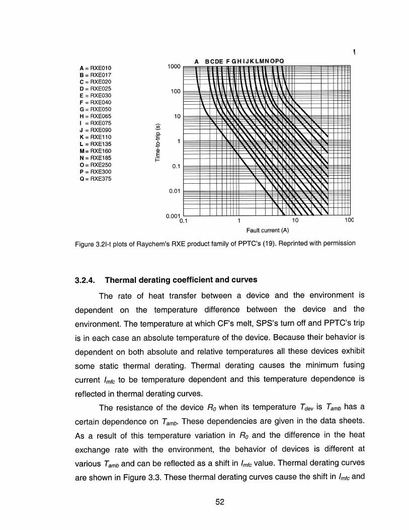
A BCDE FGHIJKLMNOPQA =RXEO1O IU UV
B= RXE017C = RXE020D = RXE025
E=RXEO3O100E = RXE030F = RXE040 u =G = RXE050 m MA 43X2 A I XiH = RXE065 10I = RXE075J = RXE090 _\1_
K = RXE110 1L = RXE135 -M= RXE160 n
E __N = RXE185 n0= RXE250 0.1P = RXE300Q = RXE375
0.01
0.00110.1 110 100
Fault current (A)
Figure 3.21-t plots of Raychem's RXE product family of PPTC's (19). Reprinted with permission
3.2.4. Thermal derating coefficient and curves
The rate of heat transfer between a device and the environment is
dependent on the temperature difference between the device and the
environment. The temperature at which CF's melt, SPS's turn off and PPTC's trip
is in each case an absolute temperature of the device. Because their behavior is
dependent on both absolute and relative temperatures all these devices exhibit
some static thermal derating. Thermal derating causes the minimum fusing
current /mfc to be temperature dependent and this temperature dependence is
reflected in thermal derating curves.
The resistance of the device Ro when its temperature Tdev is Tamb has a
certain dependence on Tamb. These dependencies are given in the data sheets.
As a result of this temperature variation in Ro and the difference in the heat
exchange rate with the environment, the behavior of devices is different at
various Tamb and can be reflected as a shift in Imfc value. Thermal derating curves
are shown in Figure 3.3. These thermal derating curves cause the shift in Imfc and
52

thus the total shift in the /-t characteristic where the interaction with the
environment is high.
150 ' ' ' ' ' I
140-10 .CF ATO
blade- 120 type0>
I 110
0 1000)-E90 -CD
0
80 - SPS f
70 - PPTC
60 -
-40 -20 0 20 40 60 80 100 120
Temperature [*C]
Figure 3.3 Temperature derating factors for three devicetypes
3.2.5. Safe operating voltage (Voltage rating)
The devices are rated to safely operate up to some voltage Vmax. This is
the voltage across the device. After the turnoff of current (end of arcing for CF)
and following a fault the voltage across the device is of the order of the source
voltage V, and therefore V, should not exceed Vmax. During the transient
behavior this voltage can be exceeded by some specified amount.
SPS's have a fixed voltage Vc, across them during the turnoff of inductive
load and this voltage Vet is the maximum voltage to which the SPS should be
subjected. SPS can take transient overvoltages higher than Vc; as described in
the data sheets. However, safe interruption of faults is not guaranteed under
these conditions. Furthermore, Infineon Technologies guarantees the safe
interruption of voltages only to some specified voltage Vmax.
PPTC's also have a maximum voltage rating at which they will safely
operate. However, during a fault this voltage can increase to a much higher value
as a result of PPTC current being unable to decrease due to presence of
53

inductance. If there is too much inductance in the circuit the PPTC will not
operate safely and might fail to interrupt a current and can potentially damage
itself.
3.2.6. Maximum fusing current (Breaking capacity test)
Maximum fusing current is the maximum prospective current that the
device can safely interrupt at some specified voltage (usually Vma). Any
prospective current larger than maximum fusing current cannot be safely
interrupted. To an extent this puts a lower limit on the equivalent series
resistance of the source and the resistance of the cable.
SPS's have a maximum fusing current defined as the maximum
prospective current that can safely exist in an SPS when Vm is connected. This
is not cited in the data sheets but is visible from their I-t graphs. The /-t graphs do
not extend beyond this point.
3.2.7. Cut-off characteristic
The cut-off characteristic is measured at a given ambient temperature and
plots the highest instantaneous current that a fuse will carry during interruption as
a function the prospective current.
In circuits where the load is purely resistive the cut-off characteristic of
PPTC's and CF's is a line with constant slope (slope is equal to 1). SPS's on the
other hand have a rather interesting cut-off characteristic. Depending on how the
fault was produced two different cut-off characteristic are produced. Both of them
are constant above a certain value of prospective current. If the fault occurs while
the device is conducting current, it takes a little bit of time for the internal circuitry
to reduce the gate voltage as described in Chapter 2. However, if the device is
turned on into a fault the operation begins with the gate voltage already lowered.
The cut-off characteristic is important because it shows the maximum
instantaneous current that can be present in the circuit. This current should be
used when calculating the mechanical stresses in the devices being protected
(motors and wires). Furthermore the instantaneous value of any transient current
peak can not exceed the value given in this graph. If such a transient current
54

peak existed without the protection device present in the circuit it would not be
achievable with the protection device present in the circuit. An example of a cut-
off characteristic is shown in Figure 3.4 for an SPS.
100C
900-
800
" 700
0 600
- 500
- 400D 300
Ex 200
10
0 200 400 600 800 1000Prospective current [A]
Figure 3.4 Cutoff characteristic of the BTS 650 P typeSPS. The higher curve obtains for the device turned onat the moment the fault occurs
3.3. New means of characterization
In order to better characterize the new devices it might be suitable to create
some new means of evaluating their performance in short circuits. Because the
CF do not have all the characteristics of the new protective devices they do not
exhibit some of the behavior that PPTC's and SPS's do. Thus, in order take
opportunity of the new functionality we need to characterize the devices with
respect to this new functionality.
3.3.1. Resetability
CF's are not resetable. Their design insures that after they have operated
under fault conditions no current will flow in the circuit till the fuse is replaced.
Thus a fuse that operated needs to be replaced. SPS and PPTC are resetable
devices. The devices can be better than fuses since they do not have to be
55

physically replaced after they interrupt a fault. If an average of 10 faults can be
expected during the life of the circuit than one would need 10 fuses for this circuit
to operate throughout its lifetime. However we would only need one SPS or one
PPTC.
The degree of resetability varies among the devices. SPS's come in two
flavors. The first kind has an automatic reset built in. When a fault occurs the
SPS will turn the circuit back on after the device temperature goes down by some
specified amount (typically 100C). The second kind has a latch function. The
device will not reset until its control input has been cycled off (on->>off->>on).
The SPS will then turn back on only if its temperature has gone down by the
above mentioned specified amount.
Only cooling can reset PPTC's. If the circuit is returned to nominal
conditions it will remain in the tripped state since the power dissipation in the
normal conditions is enough to keep the device tripped. Thus a manual shut off
of the current is needed. At this time the device cools and resets to its nominal
resistance. If the fault is removed the PPTC will again operate normally. Thus a
PPTC protected circuit must have a switch associated with it in order to utilize the
resetability of these devices
3.3.2. Modes of Failure
Under certain conditions the device might stop to operate according to its
specifications. This can occur either as a result of exceeding some specification
(such as Vmax) or because of the device reaching the end of its lifetime. At such a
time several modes of failure exist. The device can fail as a short or as an open
circuit.
A device that fails as an open circuit still protects the remaining circuit
from any fault current but it needs to be replaced. Thus this mode of failure does
not cause the destruction of the remaining elements in the circuit and resembles
the operation of the fuse. In fact, for a fuse this is the mode of operation under
fault conditions with the restriction that the fuse opens the circuit safely. Thus if
56

we exceed the voltage specified for a fuse it might fail to operate safely but will
always fail as an open circuit.
On the other hand, SPS and PPTC can fail both as open and as short
circuits staying permanently on or permanently off. This brings to question their
applicability as protection devices. If there can be found a set of conditions within
which an SPS and a PPTC will always fail as an open circuit, the boundaries of
this set should not be exceeded.
If the voltage is increased substantially across the SPS it will not be
capable of blocking the current for a long time. Once this time is exceeded it
might fail as a short or it might eventually burn itself and become and remain an
open circuit. If it remains a short this is unacceptable. Since these conditions
exist for the operation beyond the specified range of operation the safety of
current interruption is not guaranteed and can result in a fire. Thus the SPS
should never be subjected to these conditions. Similarly a fuse will interrupt a
current at V greater than Vmax but it might do it with arcs coming out of it and
setting its housing on fire or melting the contacts.
PPTC have rather strict current limitations and if this limitation is exceeded
the PPTC might fail as a short.
3.3.3. Maximum load inductance during operation and fault conditions
While the maximum load inductance is not important for PPTC's and CF's
during normal operation it is important for SPS because the SPS is the switch
that turns off the nominal current. Thus for an SPS there is a maximum load
inductance that can be present in the normal mode of operation, since the SPS
must be capable of switching it off and not destroying itself. The maximum value
of inductance for a inductance only circuit is given in the data sheets. This value
causes the highest possible power dissipation allowed in the SPS. Furthermore
the data sheets provide the value of maximum energy allowed to be imparted to
the SPS during its turnoff. Since the Voltage across the SPS during inductive
turnoff is known we can determine the turnoff 2t as a function of load inductance.
57

The maximum arcing 12t allowed for conventional fuses is measured at a
maximum value of the time constant (L/R). The maximum time constant allowed
in the circuit during a fault is given in the data sheet. If this value of time constant
is exceeded the safe interruption of faults is not guaranteed (i.e. the result might
be a fire). The reason for this limitation is explained in later chapters but the
failure mechanism is excess power dissipation in the fuse during interruption of
faults with large values of circuit time constant and consequently large
inductances.
Limitations of inductance for PPTC's are not established yet.
3.3.4. Post-trip current
SPS's with automatic reset (thermal reset) and PPTC's have some current
going through them after they interrupt a fault. The RMS value of this current is
important since it can be used to calculate the energy delivered into a faulty
circuit. The actual current for the PPTC and its RMS value are the same. For the
SPS there is a shut off followed by turn on into the fault. This can result in quite a
substantial current going into the fault. The steady state post-trip RMS current
magnitude is explored and determined in the later chapters.
It is interesting to note that even fuses often pass some current after they
have blown (although the magnitude of this current proves to be insignificant).
This is a result of the vapor deposits on the fuse housing that extend between
two electrodes after the arc is extinguished. The resistance of these paths is
rather high and is therefore almost always neglected. But Littelfuse mentions that
these currents can be in excess of several mA.
58

Chapter 4.
Theoretical and experimental
comparison of protection devices
4.1. Introduction
Using the theory developed in Chapter 2 and the characterizations
developed in Chapter 3 the performance of previously mentioned protection
devices under various changing parameters can be investigated. The changes in
the I-t characteristic due to Tamb, Vs, L, and the production process itself can be
determined. This analysis gives one the power to establish the limits of use by
plotting the worst case 1-t curves. For example, the earliest time to melt tmelt of
the given fuse as a function of prospective current lp and influenced by Tamb can
be plotted.
Before doing this it is worthwhile to investigate what happens with several
parameters in the automotive electrical distribution system as the system voltage
is increased from 14 V to 42 V.
59

4.2.42 V faults compared to 14 V faults
Changes in the system as the voltage is increased from 14 V to 42 V can
be investigated theoretically. By considering the power of the load as a constant
and the energy stored in the load as a constant certain predictions can be made.
Nominal steady state current reduces by a factor of 3. This allows the system
engineer to use a protective device with a 1/3 rating of the protection device used
in 14 V system. If the wiring is reduced so that it has the same end to end voltage
drop its resistance would increase by a factor of 3. Furthermore, one can assume
that the equivalent series resistance RESR of the 42 V source is 3 times the RESR
of the 14 V source (if the 42 V source was obtained by connecting three 14 V
sources in series). If on the other hand one assumes that the 42 V source has
the same internal power loss as a 14 V source, at a given power delivered to the
load, then the RESR and the wiring resistance both increase by a factor of 9.
Under these assumptions short circuit current on the average remains the
same (for RESR increase by a factor of 3) or is reduced by a factor of 3 (for RESR
increase by a factor of 9). Constant energy storage assumption causes the
inductance in the circuit to increase by a factor of 9. However, it is important to
note that during short circuits the load inductance is often not the important
inductance since it is shorted. Thus the inductance present in a circuit during a
short circuit is primarily due to the stray inductance of the connecting cables and
to first order this remains the same as source voltage changes (detailed analysis
of cable self inductance is presented in Chapter 5).
4.3. Variations in 1-t plots of protection devices due to
various effects at constant ambient temperature
The purpose of this section is to investigate the variability of melting and
initial turnoff /-t plots for CF's, SPS's and PPTC's at constant ambient
temperature. These I-t plots do not include the turnoff of inductive faults. Since
the governing factor for this part of the operation is current and its magnitude, the
introduction of a higher source voltage causes no changes in operation of
60

protection devices. Therefore, the analysis is done at 12 V and any change in
source voltage to 42 V will not cause a change in the results here obtained if the
prospective currents under consideration are the same.
Since it would be impossible to investigate each fuse separately one fuse
type and rating is considered. Generalizing the obtained results is trivial. The
fuse chosen as a test case is the ATO type automotive blade fuse with Inor=1 OA.
The particular fuse under considerations is manufactured by Littelfuse (6). The
1 E+6
1 E+5
1E+4
1 E+3E- 1 E+2
1E+1
1 E+0
1E-1 1 10 100 1000Current [A]
Figure 4.1 -t plot for a ATO blade fuse with Inom=10A
published average melting I-t graph of this fuse is shown in Figure 4.1 Data for
the Figure 4.1 comes from Reference (6). Using the data sheet one also finds
that minimum value of Imfc is 11 A (6). Thus, the hold current /hold is 11 A and this
corresponds to a minimum fusing factor of 1.1.
The purpose of this investigation is to determine the fuse performance
variations due to production process but at constant ambient temperature
Tamb=25 0C. The minimal melting 12t for this fuse is 115 A2 s (6). However the
published average melting 1-t curve reveals an average melting 12t (in high
current region of operation) to be 122 A2 s. In order to obtain a minimum melting
/-t graph (hold characteristics) at Tamb=25 0C the values of current for any given
time should be multiplied by the square root of the ratio of melting 12fs. Thus a
following relationship obtains for shifting any given point (/p, t) from the average
melting /-t curve to a minimum melting 1-t curve:
61
......... .. .......
....... .....

(/p, t)@(Tam-250 C, average melting 12t) +
4 (lp*[(minimum melting ft)I(average melting ft)]0 5 , ty) @
@(Tamb=25 0C, minimum melting 12t) (4.1)
This shifting procedure works in the high current regime of operation
because the melting ft value for a given fuse is constant at high currents. The ft
in this regime of operation is proportional to the energy necessary to melt the
fuse. Therefore, a fuse with lower melting ft needs less energy to melt in a given
constant amount of time. Since energy delivery is proportional to current, a fuse
with lower melting ft needs less current to melt in a given constant amount of
time.
While it is inherently obvious why the above-explained shifting procedure
works in the region where ft is constant (high current faults), further explanation
is necessary for the region where the interaction with the environment takes
place. When the heat loss to the environment is present, the values of ft
associated with any given /p represent both the energy required to melt the
fusible link and the energy exchanged with the environment. Examnination of
Equation 2.1 shows that production variations cause a change in the energy
necessary to melt the fuse and energy exchanged with the environment by the
same relative amount ( for detailed analysis refer to Appendix A). For example,
let's investigate the case where (melting ft)=10*(average melting ft). The
energy exchanged with the environment is proportional to 9 times the average
melting ft. For a given time tv and temperature Tamb the 9:1 ratio between the
energy exchanged with the environment and energy used to melt the fuse
remains constant under the theory explained in Appendix A. Manufacturing
variations change the amount of power dissipated in the fuse for a given amount
of current. Energy is proportional to ft values. Thus, the current necessary to
melt the fuse in a given constant amount of time changes. ft values differ both
for the melting energy and the energy exchanged to the environment. However,
The ratio is the same if constant time is assumed.
62

Furthermore, the distribution in melting 12t values A( 2t) can be determined
by subtracting the minimum melting 12t from the average melting 12t. Now if we
assume that the distribution of melting f2 t is symetric and finitely bounded by the
production process we can determine the maximum melting t2 t by adding the
A(Ft) to average melting 12t. Now we repeat the shifting process of Equation 4.1
with obvious changes to the 12t values to obtain the upper limit for the fuse 1-t plot
at Tamb=25 0C. This gives us the trip characteristic. The trip characteristic depicts
the minimum I-t plot for which all the devices with the same part number will trip.
The variations are due to production process variation. The average melting /-t
plot together with trip and hold /-t plots is shown in Figure 4.2. Figure 4.2 shows
that it is it is almost impossible to distingush between the trip and hold
characteristics of a fuse. This is a result of extremely tight tolerances in the fuse
production process.
104
,103
E102
F101
100
10-1
10-
10-
101 Current [A] 102
Figure 4.2 Variations in 1-t plots as a result of variations in fuse productionprocess for an ATO 10A fuse
The production process of an SPS causes a variation in several different
parameters affecting the performance of an SPS. The manufacturing process
creates a range of different cold resistances Roodtand current limits /,,pat a given
ambient temperature. After these variations are all accounted for a hold and a trip
I-t curves can be created for a given Tamb. A hold characteristics insures that any
device with a given part number will not trip before reaching this current. The trip
characteristic ensures that all given devices will trip at least according to this
63

curve or before. Alfons Graf examined these variations and their influence on the
1-t curves (11). It would be pointless to repeat the procedure and replicate the
results. However, for the reasons of comparison some examples of the results
are replicated here.
Dependence of the RoN -typical -RO min Dependence of the IL(scp) max.rftnt oitBTS 733 L1 -RON max BTS 733 li -typical
E
IE+6 -_ _ _ _
IE+5 - . -
IE442
1 E+1 _____
l...........
I E+6 . ....
1 E+4
1 E+3
1 E+2
E1
1o current in A 0oo 1C00 1 10 currentInA i 1000
Figure 4.3 Dependence of production parameters such as Fn and I, on SPS 1-tcurve (11). Reprinted with permission
Figure 4.3 shows the variations due to the differences among devices of the
same type caused by the production process parameters such as 1,p and Rood
for all devices at the same ambient temperature. RooId has the strongest influence
in the regimes of operation where the SPS is operating in the linear region of its
mosfet characteristics. The /sep has the strongest influence on the regimes of
operation where the SPS is operating in saturation region of its mosfet
characteristics. These two plots combined give the hold and trip characteristic of
the SPS as a result of production process variations.
In comparison to the conventional fuse of similar current rating the
performance variations due to production process in the high current region of
operation are much more substantial for the SPS. The variations in the region
64
I E+5 1....................... ..... ............
. ...... ...
................
. .............
...................
Vps

where the exchange of energy with the environment is substantial are
comparable to the conventional fuse but slightly larger in magnitude.
The production process also affects the performance of PPTC's. Many
things can vary in the production process of a PPTC. For example, the amount of
conductive particles relative to the amount of the polymer and the dimensions of
the PPTC can be altered during the production process.
Furthermore, increased post trip resistance of the PPTC as compared to
the resistance prior to tripping will also influence the performance of any given
PPTC. After the PPTC trips it has higher resistance that the PPTC that never
tripped. Higher resistance causes higher power dissipation for the same amount
of current and results in faster tripping times. While this is not an effect caused by
variations in the production process, it is an effect that affects performance at
constant temperature and causes the performance variation between a group of
PPTC's of the same part number.
A hold and a trip characteristics that account for all possible variations in
performance at Tamt=2 0*C for devices with the same part number can be
determined. These two characteristics are a result of both the variability of the
production process and the difference in post trip resistance compared to
minimum resistance. To obtain the hold and trip characteristics a shifting
procedure similar to the shifting in the fuse case needs to be performed. The
data sheets give an average I-t characteristic. By shifting the average /-t
characteristic to the location of the hold current 'hold, the hold characteristic
obtains. Similarly, the trip characteristic is obtained by shifting the average I-t
characteristic to the location of the trip current /tip. Again, as in the SPS and CF
case, any given device is guaranteed to trip above 'trip and no device will trip
below 'hold. Data sheets for PPTC's contain the values of average turnoff I-t plots
as well as the 'trip and /hold (19)
Thus at Tam=2 0 0C we can right away notice from the data sheets that the
fusing factor for a PPTC from a group of PPTC's with the same part number can
vary from 1 to as high as 2. This follows from the fact that a device could be used
with nominal current /nom as high as the hold current 'hold and still in the worst
65

case the resulting fusing factor would be the ratio between /trip and 'hold. Thus, the
performance variations produced due to the post trip resistance behavior of
PPTC's and the production process variations, show that the PPTC's have the
biggest gap between the hold and trip characteristic of all three protection device
types. All the performance variations examined in this section were performed at
constant temperature. An example of PPTC's trip, hold and average I-t
characteristics is shown in Figure 4.4.
1 E +7 rI7 ....... ......
1E+6
-- 1E+5E
E1 E+4
1 E+3
1 E+21 10 100
Current [A]
Figure 4.4 Hold and Trip characteristic for the RUE 400 PPTCdevice at Tamb= 2 50C.
In conclusion, the CF exhibits the smallest performance variation at a given
constant ambient temperature. Due to the simplicity of CF construction many of
the parameters influencing the pre-arcing performance of conventional fuses can
be tightly controlled.
4.4. Variations in 1-t plots due to changes in ambient
temperature
Up to now, the variations in protection device performance due to various
effects were calculated and compared at constant ambient temperature. In the
66
............................. ...............
............................ ..................................... .............
.............. ............ .......................... ..................................................... .................. ............
............ ............ ..................... ................ ................ .....
............
.... ..................... ................
..................................... ........................... ................................... ...................
...................................... .................... .............................. ..............
..............
............................

automotive electrical environment the protection devices are required to operate
over a wide range of ambient temperatures. In the passenger compartment the
ambient temperatures vary from -400C to 850C. In the engine compartment the
ambient temperature can vary from -40C to 1250C. In order to use the devices
in such extreme temperature ranges melting I-t plots for CF's and initial turnoff -t
plots for SPS's and PPTC's at various temperatures need to be determined.
Furthermore, hold and trip characteristics at the extremes of these temperature
ranges also need to be established.
In order to calculate the -t plot for a fuse at any ambient temperature the
shiffting procedure of Section 2.3 must be done. To use the shifting procedure
the ratio of I2fs at different temperatures has to be determined. The 12t at
Tamb=25 0C is given in the data sheets. To obtain the Ft value at any other
temperature Equation 2.4 has to be solved. This can be done through the use of
numerical methods and various computer programs. In this research Matlab was
used to solve the Equation 2.4. The assumption of constant temperature
distribution across the fusible link is justified by the fact that pre-arcing times are
short in the high current regime of operation (4).
Performance variations described in Section 4.3 are again present at any
104
102 -Tamb=-40*C
10)
10-2 Tamb=12 5 *C
101 102 103Current [A]
Figure 4.5 Temperature variations in the /-tcharacteristics for an ATO 1 OA fuse
67

given ambient temperature. This results in separate average, hold and trip /-t
plots for any given temperature.
Thus by using this method the I-t plot variations across any temperature
range can be determined. The 'fastest' curve is the hold characteristic at highest
ambient temperature. On the other hand, the slowest curve is the trip
characteristic at lowest ambient temperatures. The results of applying this
analysis method is shown in Figure 4.5 for the temperature range applicable to
the automotive engine compartment ambient temperature range specifications.
However, if a fuse utilizes diffusion pill technology then it needs to be
examined differently. In the region of operation where 12t is constant, the critical
temperature is the melting temperature of the fusible link material (typically Zn or
Cu). As fault currents approach the minimum fusing current /mfc, the critical
temperature to be used for calculations is the melting temperature of the diffusion
pill material (typically solder). Thus when determining the shifts in I-t plots
caused by the change in Tamb two critical melting temperatures must be utilised,
melting temperature of the fusible link material and melting temperature of the
diffusion pill material. This produces two new values of 12t and two ratios with the
unshifted ft. The ratio produced with the melting temperature of fusible link is
310
210
Tamb=-40*C
E 10
E
- 100 Tam=25C
10 Tamb=125'C
102 3
10 10 10Current [A]
Figure 4.6 Effect of the ambient temperature changeon the I-t characteristic of a 20A MAXI fuse
68

used in regime where 12t is constant. The other ratio is used in regime where the
interaction with the environment is high (for fault currents just above /mfc). This
procedure applies for the slow blow fuses such as the MAXI fuses. The results
for a 20 A MAXI fuse are shown in Figure 4.6.
The performance of SPS's is also influenced by changes in ambient
temperature. These changes are a result of the thermal properties of silicon. This
was shown in Chapter 2 where the effect of temperature on the SPS I-V
characteristics was presented. Alfons Graf from Infineon Technologies
investigated the effect of ambient temperature influence on the performance of
SPS's. His results are in the form of I-t plots with hold and trip characteristics at
two extreme temperatures in the passenger compartment automotive electrical
environment. The procedure for generating ambient temperature performance
variation data will not be repeated since it can be found in References (11,14).
An example will be presented for the sake of completeness of this section.
Figure 4.7 shows the temperature dependence of I-t plots as a function of
BTS 733 L1Worst case including tflP t o
temperature-range -40*C to 85*- typical at 25*C1E+6---
v= 13v
1E+4 Switch offarea
E+
operating1 E+2-
1 10 currenenA 1oo Wo
Figure 4.7 Worst case dependence of I-t plot for theSPS accounting for all parameter variations andtemperature operating range (11). Reprinted withpermission
69

temperature. Again, as in the CF case the fastest acting curve is the hold
characteristic at highest ambient temperature. The slowest acting curve is the trip
characteristic at lowest ambient temperature.
It is interesting to note that the operating ambient temperature range in this
plot is the operating ambient temperature range of the passenger compartment.
Thus by comparing Figure 4.7 with Figure 4.5 it is obvious that the performance
variation for a CF is much smaller than for the SPS as a function of ambient
temperature. This is a result of much smaller critical temperature for the device
operation. The critical temperature for conventional fuses is the melting
temperature of the fusible link (greater that 4000C for Zn). On the other hand the
critical temperature of the SPS is the junction temperature Timax at which turnoff
begins (Timax-150 0C). Consequently, the CF's have less performance variation
due to changes in operating ambient temperature. If the conventional fuse
utilizes the diffusion pill technology, then the critical temperature for fault currents
close to /mfc is comparable to the critical temperature of the SPS. The
performance variations in this regime of operation of the two devices are in that
case comparable.
Because PPTC's have nonlinear temperature dependence they do not
thermally derate in the same manner as CF's do. Their static thermal derating
curve tends to be constant but having a much higher slope (Figure 3.3). This
thermal derating can be directly applied to the regime in which there is a lot of
interaction with the environment. In this regime we know that for a given current
/p it takes time trip for the device to trip at a given ambient temperature
Tamb=25 0C. If the temperature changes the current also changes by the thermal
derating factor while the time remains the same.
However, for high current faults PPTC do not have a constant 12t and
calculating the appropriate 12 t for the device at a different temperature and
current becomes hard due to nonexistence of a simple theoretical model for the
behavior of PPTC's. Experimental results exist for typical devices and they can
be used to guide us in determining the worst case I-t plots for a PPTC in some
operating temperature range. The experimental results exist showing best and
70
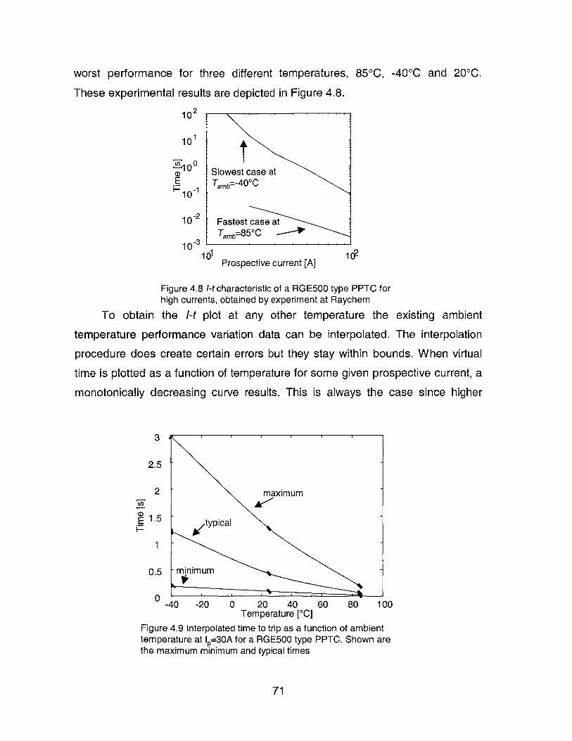
worst performance for three different temperatures, 850C, -400C and 200C.
These experimental results are depicted in Figure 4.8.
102
10
10
I10-
10-2
10-3101Prospective current [A]
i?
Figure 4.8 1-t characteristic of a RGE500 type PPTC forhigh currents, obtained by experiment at Raychem
To obtain the /-t plot at any other temperature the existing ambient
temperature performance variation data can be interpolated. The interpolation
procedure does create certain errors but they stay within bounds. When virtual
time is plotted as a function of temperature for some given prospective current, a
monotonically decreasing curve results. This is always the case since higher
3
2.5
2
i~ 1.5
1
0.5
0 -40 -20 0 20 40 60 80 100Temperature [*C]
Figure 4.9 Interpolated time to trip as a function of ambienttemperature at Ip=30A for a RGE500 type PPTC. Shown arethe maximum minimum and typical times
71

temperature always results in shorter tripping time for a given device and
prospective current. Thus our interpolation procedure creates minimal error as
long as the resulting time versus temperature plot is monotonically decreasing.
Figure 4.9 shows interpolated times as a function of Tamb for a given prospective
current. The curve labeled as maximum time curve, represents a data point of
the trip /-t characteristics as a function of temperature. Correspondingly, the
minimum curve represents the data point of the hold /-t characteristic as a
function of temperature.
Performance variations caused by the changes in operating ambient
temperature of the PPTC are the largest of all three protection device types. This
is a result of the PPTC having the lowest critical temperature (Ttrip ~125oC). As a
result of this low critical temperature the PPTC may not even be capable of
working in the automotive engine compartment. By some automotive standards
the highest operating ambient temperature in the engine compartment is 1250C.
If we placed the PPTC in this environment at this highest temperature it would
trip without having any current present in it.
Considering both the impact of ambient temperature changes and other
effects (which are present from sample to sample at any given temperature), the
conventional fuse has the smallest performance variation. SPS's have
comparable performance to slow blow fuses utilizing diffusion pill technology.
PPTC's have the largest performance variations of all three protection device
types and the largest gap between the hold and trip /-t characteristics.
4.5. Comparison of performance during turnoff of fault
currents in circuits with inductive loads
If there is inductance present during fault conditions, the current cannot be
turned off until the energy stored in the inductance has been dissipated. The rate
at which the current is turned off is a function of the voltage across the inductor.
In a purely inductive fault the voltage across the inductor is the difference
between the source voltage and the voltage across the protection device. Thus
72

the performance in inductive circuits will change when the system voltage goes
from 14 V to 42 V.
For conventional fuses the introduction of inductance changes both the pre-
arcing and the arcing behavior. Due to the fact that -t plots show virtual time, the
pre-arcing period remains the same for a given ambient temperature. The arcing
time is determined from the maximum allowable arcing 12t measured at maximum
allowable circuit time constant Lc/Rc. This limit is specified by the manufacturer
(6). Arcing 12t only adds to the characteristic by adding time at a given /p. It is
104-Clearing at
102 Tat=-40*C
a>- 100
10-2 Melting atTatA=-40C
101 1 02
Current [A]
Figure 4.10 Effect of Arcing 12t on the ATO 10A fuseperformance
important to realise that the /-t plot is shifted vertically for adding the arcing 12t.
The reasoning for this comes as a result of the realization that /mfc remains the
same since arcing never comences if the current in the fuse is exactly the
minimum fusing current. The time added is thus virtual time obtained by dividing
the maximum arcing 12t by the square of /p. Difference between clearing
(melting+ arcing) and melting -t plots is shown in Figure 4.10. Since arcing times
are extremely short for the fuse under consideration, it seems that arcing time is
insignificant and can be neglected. However, other automotive fuse types, such
as the MAXI and MEGA fuses by Littelfuse, have longer arcing times that should
not be neglected when the performance is evaluated.
73

However, arcing 12t is also a measure of energy imparted on the fuse and
thus the maximum arcing 12t should not be exceeded. We can calculate the
I 2tarcng by making certain assumptions about the behavior of fuses during arcing
previously described in Chapter 2. Then, the 12t of an exponentially decaying
current is equal to the initial current squared multiplied by the time constant of
decay. Note that the time constant for decay of t2 is the time constant for
decay of / . Under these assumptions and using the previously introduced
terminology the following equation holds:
I2 t - KI ,' V S -OR cold /0arcing VO -0 Rcold /
where K and 6 are constants used to achieve better fit with experimental
data, lo is the current at the beginning of arcing, Rot, is the cold resistance of the
fuse, Vs is the source voltage Vo is the initial voltage across the fuse at onset of
arcing and ris the circuit time constant.
30
25
20
M 15
.10 -0). 5
< 0
-5
-10
-15''0 250 500 750 1000
Prospective current /, [A]
Figure 4.11 Arcing 12t for an ATO 10A fuse when -is kept constant
By solving Equation 4.2 for a maximum allowable t given in data sheets
(Figure 4.11) and Vs=13 V we notice that the maximum arcing t2t occurs for only
one value of /p. Thus keeping the rbelow this will insure that the maximum arcing
t2t is as specified in the datasheet. However, one can calculate the value of T that
74

results in the maximum allowed arcing 12t as a function of prospective current.
The circuit designer needs to guarantee that any possible fault does not exceed
the maximum value of r allowed at that fault current. This insures that the power
dissipation limit of this particular fuse design is not exceeded during arcing in any
possible fault condition.
Figure 4.12 shows the relationship between z and /p calculated by solving
Equation 4.2 for I2tarcing set to maximum allowed and kept constant.
101
W 100
V 10-1
10-2i~~
10-3
0 250 500 750Prospective current I, [A]
Figure 4.12 Maximum allowable time constant as afunction of /P for an ATO 1 OA fuse
Based on this theory, if it can be assumed that the prospective current will
be limited to a range which does not include the minimum value of r in Figure
4.12, it would be justified to use the fuse in a circuit with a larger value of z. The
larger value of r would be the minimum value of r in the range of prospective
currents that can exist in the circuit and could be obtained through Equation 4.2
or from Figure 4.12.
Despite this possibility, suppliers of fuses specify in their application
literature a maximum r, independent of the range of prospective currents. The
limitation of r given by the manufacturer insures that maximum arcing 12 t is never
exceeded. Figure 4.13 shows this limitation as the function of load resistance and
load inductance during faults. Product design dictates adherence to this
75

guidance, unless robust empirical evidence, and not just this theory,
demonstrates that another practice is safe.
The investigation of effects of higher source voltage have not been
performed yet since the first automotive fuses rated to operate in 42 V
environments are either in the prototyping phase or have just shown up on the
market.
COC
(0
1
0.9
0.8
0.7
0.6
0.5
0.4
0.3
0.2
0.1
00 0.2 0.4 0.6 0.8 1
Circuit inductance Lc [H] x 10
Figure 4.13 Inductance limitation for an ATO 10A fuse underthe constant t limitation given by the manufacturer.
The application notes published by Infineon Technologies do not cover the
turnoff of current by the SPS for faults that contain inductance. Thus, it is
interesting to investigate this effect further. The inductive turnoff for an SPS was
completely described in Chapter 2 and it is therefore straightforward to calculate
the 12t associated with it. By integrating Equations 2.9a and 2.9b we obtain:
2t = aL a3 1 a )+ a _ 2] in generalVC - Vs1 1 +a 2
/2t = - LClo033 Vc - Vs
assuming a purely inductive load
(4.3a)
(4.3b)
where a is given by:
V -Va= cVsIVs - R0lo
a> 0 when operating within specified limits
76

However, since Equation 4.3a always gives values smaller than Equation
4.3b the worst case is computed by using Equation 4.3b. Combining Equation
4.3b with the Equation for the energy 2.10b and solving by using a given
maximum allowed energy we obtain the following simple equation for arcing 12t
/2t =2 Emax/O (44)3 VL
And again by the standard procedure we divide this "arcing" 12t by the
square of prospective current and add the resulting virtual time to our /-t plot.
Figure 4.14 shows /-t plot of virtual time during turnoff of an inductive load as a
function of prospective current for an SPS.
To put the necessary limits on the maximum value of inductance in any
0.1
E
EH- 0.01
0.001
0.0001
1 10 100 1000 10000Prospective Current [A]
Figure 4.14 Virtual arcing time as a function of prospectivecurrent for a BTS 550 P assuming V=13V and Emax=1.2J
given situation we can plot Rc versus Lc graph (figure 4.15) that shows the
energy boundary obtained from Equation 2.1Oa and tells us the allowed Lc at any
given value of Rc. Thus, to use the devices properly it is important that any fault
condition that can occur does not fall in the forbidden region since that would
result in the destruction of the SPS. Furthermore, unlike a fuse, the SPS must be
77

1
0.9
0.8 -======
~0.7
~0.6
0
0.5
S0.4
~0.3... .
they oo shuld aso fal in healo den ofa-il theot inFiue4.5
0.2
0. 1
00 0.002 0.004 0.006 0.008 0.01
Inductance in the circuit Lt [HIFigure 4.15 Allowed values of resistance c and inductance Lo in any mode of operationfor a BTS 650P type SPS.
capable of switching off the nominal load R and nominal inductance L and thus
they too should also fall in the allowed region of the plot in Figure 4.15.
In comparing the inductance limitations of the SPS to the inductance
limitations of the CF we can compare Figure 4.15 with Figure 4.13 and notice
that at source voltage of 14 V SPS can deal with a lot more inductance during
fault interruption. As the source voltage is increased, the SIPS will be less
capable of dealing with fault and normal load inductances. This is a result of the
fact that SPS's designed to operate in the new 42 V environment develop a 60V
voltage drop across themselves during the turnoff of inductive currents.
In case of the 14 V system the negative voltage that appears across a
purely inductive fault load is 46 V. In a 42 V system the negative voltage across
the inductor would only be 18 V. Thus one can conclude that it will take longer to
dissipate the energy stored in the inductance. However, at the same time the
power dissipation in the SIPS is proportional to the product of 60 V and the
78

current in the SPS. The exact equation that gives the limitation on load
inductance Lc as a function of voltage across the SPS Vi, the source voltage Vs,
energy dissipation limit E and load resistance Rc is given by:
LC 2- -R (VCL -VS) (4.5)VCL - V2
If the value of inductance given by the above equation is exceeded the
energy dissipated in the SPS will exceed the safe value and the SPS will fail.
Using the above equation a plot of maximum allowed inductance versus
resistance in the circuit can be generated. An example of this plot was shown in
Figure 4.15. Figure 4.16 shows the maximum inductance versus the load
resistance as a function of two source voltages. As the source voltage is
increased from 14 V to 42 V the allowed inductance present in the circuit is
1
0.8 - V,=42 V
0.6
0.4 Vs=14 V
0.2
C0 X 100 0.5 1 1.5 2
Inductance in the circuit Lc[H]
Figure 4.16 Inductance limitation as a function of circuitresistance for BTS 410 E2 type SPS. Results for twosource voltages are shown.
reduced by the ratio of voltages appearing across the inductor in the two
systems. For the SPS's rated to operate in 42 V EDS the maximum allowed
inductance at any given load resistance is reduced by a factor of about 4
compared to operating the same switch in a 14 V EDS.
The limitations of inductance of the new 42 V fuses have not been
established yet. Once they are established they will not prove to be better than
79

the limitations at 14 V case. In order to perform the comparison of performance
between fuses and SPS's these limitations need to be established by the fuse
manufacturers. Since each fuse manufacturer will have his own strategy for
making automotive fuses rated to operate in 42 V systems, it is hard to predict
the performance of future automotive fuses during turnoff of currents in circuits
with inductance present. According to Section 4.2 the load inductance could
increase by a factor of 9. In that case many of the inductive loads that did not
create problems during fault conditions could start to pose problems for both
conventional fuses and SPS's. Without a standard for performance in inductive
faults, future automotive fuses might not be interchangeable among different
manufacturers.
The limitations on load inductance during fault conditions have not been
established for PPTC's. The complexity of the theory of their operation poses a
problem for establishing this limitation. However, one can surely say that the
limitations will be lower as the source voltage is increased to 42 V. Since the fault
inductance already is a problem in certain 14 V circuits, it can be expected that
the problem will be even more apparent in the future 42 V system.
4.6. Comparison of power dissipation of protection
devices in normal mode of operation.
The space allocated for the protection devices in the automotive electrical
junction boxes is getting smaller and smaller. On the other hand, the number of
circuit to be protected is constantly getting bigger. As the result of these trends
the protection devices are closely packed together next to each other. If the
power dissipation of the protection device is too high the protection device will
generate too much heat in its near vicinity. In order to compare the protection
devices with respect to heat that they generate an investigation of power
dissipation needs to be performed.
All protection devices behave as resistors during the normal mode of
operation (no fault is present). Even in normal mode of operation the devices
80

heat up. Because the devices operate at some temperature higher than the
ambient temperature, their resistance changes and affects the power dissipation.
Conventional fuse manufacturers publish typical voltage drop across the
fuse when nominal current is present in the fuse. The product of this voltage drop
and nominal current is the power dissipation in normal mode of operation. Using
data published by Littelfuse a plot of power dissipation as a function of nominal
current is generated in Figure 4.17 (16).
4
3.5
3Littelf use
2.5
1.5 PudenzS1 *
0.5
00 10 20 30 40
Nominal Current /, [A]Figure 4.17 Power dissipation of the fuse as a functionof nominal rated current. Results shown are forLittelf use 32 V ATO type standard fuses and Pudenz 58V FKS type fuses.
Furthermore, preliminary data for Pudenz's 42 V automotive fuses is plotted
as well. The new 42 V fuses rated to operate at 58 V have the same power
dissipation as the old 14 V fuses. Thus they do not present any new thermal
problems that do not already exist in the fuse boxes today. These Pudenz 58 V
automotive fuses are different from previously mentioned 80 V Wickmann's blade
type fuses (Chapter 2). They have roughly the same cold resistance as
Littelfuse's ATO type fuses for a given 1mfc.
In the 42 V system the fuse necessary to protect the load of the same
power has one third of the rating of the 14 V fuse as discussed in Section 4.2.
That implies that the power dissipated in the fuse for a load with given power
goes down by a factor of 3 as the source voltage is increased from 14 V to 42 V .
81

However, one should keep in mind that 42 V automotive blade fuses are not
standardized yet. It can be expected that a standard for a blade type fuse for the
42 V EDS will be established among the fuse manufacturers and auto makers.
As such a standard is reached the above conclusions might become invalid.
Future 42 V automotive fuses could have power dissipation higher or lower than
the Pudenz's 58 V fuses presented here.
However, if the standardized 42 V fuses end up having power dissipation
higher at 42 V, they will most probably be capable of dealing with higher load
inductances. This conclusion is a result of the theory of fuse arcing presented in
Chapter 2. If the fuse resistance is higher the constricted portion of the fusible
link is longer. This longer constricted portion develops a longer arc. A longer arc
implies higher voltage drop across the fuse and consequently faster interruption
of current. If the current is interrupted faster, the source can deliver less energy
into the fault. Consequently, the fuse is capable of discharging higher energies
stored in circuit inductances without exceeding its own power dissipation limit for
safe interruption.
There is no standard way to calculate power dissipation of SPS's at their
nominal current. The addition of the heat sink to the SPS changes its thermal
resistance, which changes both the nominal current and the power dissipation of
the SPS.
In order to create some data to compare with conventional fuses device is
assumed to be in Tam= 250C. The junction of the device is presumed to be at
Tjmax=1500C and power dissipation is plotted as a function of current. Because
the temperature of the device is considered to be constant as power dissipation
changes, different points on such a plot represent different values of thermal
resistance Rthja. In order to change the thermal resistance of the device, a heat
sink needs to be introduced to the casing of the device. Because the operating
temperature chosen is the threshold between tripping and normal operation,
power dissipation is plotted as a function of minimum fusing current Imfc. Each
value of minimum fusing current and power dissipation corresponds to a certain
heat sink.
82

25
S20
c.0 15 No heat sink
10
59 -
05 10 15 20 25
Minimum fusing current Imfc[A]
Figure 4.18. Power dissipation as a function of minimumfusing current for BTS 640 S2 type SPS. Minimum fusingcurrent changed by addition of heat sink. Smallest valuerepresents no heat sink.
Figure 4.18 depicts power dissipation of a given SPS as a function of /rnfc.
Both the power dissipation and the /mfc are altered by addition of a heat sink. As
the Figure 4.18 shows, the power dissipation increases as /mfc is increased by
addition of the heat sink. As Imfc is increased the thermal resistance is reduced.
The minimum value of power dissipation is given at minimum value of rfc. The
minimum value of Imfc results from the device with no heat sink present and
therefore highest value of thermal resistance.
However, in order to compare the power dissipation of SPS's with the
power dissipation of CF's, power dissipation of each available SPS with no heat
sink present can be plotted as a function of Imfc. Figure 4.19 depicts both the
power dissipation of SPS's (without heat sinks) and power dissipation of CF
sorted out by type of device (SPS or CF) and the voltage rating (rated for 42 V
EDS or for 14 V EDS).
Figure 4.19 shows that the power dissipation of currently available SPS's is
larger than the power dissipation of CF's with similar /mfc's. Thus, the voltage drop
across the SPS and consequently its resistance at given minimum fusing current
is higher as well. If the voltage drop between the load and the source in the car
becomes more restricted in the future dual voltage automotive environment the
SPS will present more trouble in meeting these new specifications than the CF
83

4.5
4 - --- ------ SPs
3.5 .3 - Rated for 42 V system
- Rated for 14 V systemA- 3 - c-. ------- CF2.5 - . ORated for 42 V system
-2 -- (from Pudenz)
M- + Rated for 14 V system1.5 (from Littelfuse)
0.5 -
00 5 10 15 20 25 30 35
Minimum fusing current /mc [A]
Figure 4.19 Comparison of minimum power dissipation as a function onfor SPS's produced by Infineon and conventional fuses. Parts rated tooperate in both 42V and 14 V systems are shown
will. The on-state resistance of the SPS can be reduced by the use of the bigger
MOSFET. Unfortunately, this even further increases already unfavorable cost of
the SPS's.
As the system voltage is increased to 42 V, the power dissipation of a given
SPS in normal mode of operation remains the same for the same /mfc. Since a
given SPS is capable of a given on-state resistance RDS, the power dissipation
will decrease if the same device is used for a 42 V load with the same power
consumption as the 14 V load. Alternatively, a smaller MOSFET can be chosen
for the 42 V loads. Thus, for a given power of the load the power dissipation of
the protection SPS is reduced as the system voltage is increased from 14 V to 42
V as a result of reduced load current.
In order to theoretically predict the power dissipation of a PPTC, a good
theoretical model is necessary. Due to nonexistence of this theoretical model and
lack of comprehensive experimental data given by the manufacturer, simple
experimental measurements were performed. The details of the experimental
setup can be found in Appendix B . Since only a limited number of devices were
tested the data represents power dissipation values for typical devices only and
worst case and best case values cannot be extrapolated without more systematic
testing that would cover the device performance variations due to manufacturing
84

process. As was explained in Chapter 2, after the PPTC trips its conducting-state
resistance is substantially higher than the conducting-state resistance prior to
tripping. This increased post-trip resistance causes higher dissipation in devices
that have tripped.
Power dissipation was measured at published hold current for the device.
This is the highest nominal current that can be systematically used in
applications. Figure 4.20 plots the measured power dissipation of two PPTC
types with different maximum voltage ratings as a function of hold current. The
power dissipation of conventional fuses is also plotted for comparison. One can
see that the devices rated to operate up to 60 V and suitable for the 42 V EDS
have higher power dissipation than the devices rated for 14 V EDS. The power
dissipation of devices rated for the 14 V EDS is comparable to the power
dissipation of CF.
-,- 1------ ------ ~~ ------------~~~- PPTC's rated for 14 V EDS....................................0Power dissipation prior to tripping
0.8.-.--.- -.................... . 0 Power dissipation after tripping
.-------- .. PPTC's rated for 42 V EDSo. 0.6 0 Power dissipation prior to tripping
S0 Power dissipation after tripping
0.4 ~CF's rated for 14 V EDS
0 V Power dissipation of CF's- 0.2
00 5 10 15
Hold current Ihold[A]
Figure 4.20 Experimentally determined power dissipation of PPTC prior to tripping andafter at least one trip as a function of hold current. PPTC's rated for both 42 V and !4 Vsystems are shown. Power dissipation of fuses is plotted for comparison.
However, since the power dissipation of PPTC's is different for devices that
have undergone a trip and the devices that have never been tripped before, two
different data points were measured for each PPTC device tested. One data
point represents the power dissipation of the device that has not tripped. The
second data point represents the power dissipation in the PPTC one hour after
the device was tripped and allowed to return to its low resistance state. The
85

experimental data verifies the increased power dissipation of devices that have
just tripped and reset to their normal state. This is predicted by the increase of
the post trip resistance explained in Chapter 2.
4.7. Post-trip current for resetable devices
Both, PPTC's and the auto resetable SPS's have post-trip current present
after they have tripped. Since this current is delivering energy into the faulty
circuit, the investigation of the magnitude of this current was performed to
determine the possible impact of this current on the circuit.
Certain SPS's automatically restart after a fault. It is important to evaluate
the post-trip RMS current of these devices. The post-trip current can be
determined theoretically by averaging the circuit behavior.
An auto-resetable SPS operates by heating up to the critical temperature
and then turning off. After it turns off it waits for the temperature of the SPS to fall
100C under the critical temperature and turns back on. Figure 4.21 shows the
60
S40
0 20
0 -0.2 0 0.2 0.4 0.6 0.8 1 1.2Time [s]
Figure 4.21. Experimentally recorded SPS currentduring the interruption of the fault current. Data shownis for BTS 640 S2 type SPS produced by Infineon.
actual value of the current as a function of time recorded using the experimental
setup. Figure 4.22 is the blow up of a small portion of the waveform in Figure
4.22 after steady state is reached. Form these two figures one can see that there
is the initial constant current regime which represents the heating up to initial
86

40
30
20
10
0 3 3.01 3.02 3.03 3.04Time [s]
Figure 4.22. Blowup of the experimentally determinedwaveform shown in figure 4.21 after thermal steadystate is reached.
turnoff and the regime where the device keeps turning off and on and the current
is pulse width modulated (PWM) according to the thermal behavior of the SPS.
By averaging this PWM behavior a theoretical model can be obtained. In
this average model the device is considered to be at constant temperature above
ambient which is 50C less than the Tjmax. By assuming that the device is at Tmax
the error introduced is minimal. In order to keep the device at Timax certain power
needs to be delivered to the device. This power is just the power delivered to the
device at /mfc given by mfc*Rdev@T=150.
During the automatic turnoff, the same power needs to be delivered to the
device in order to keep it at Tmax. Thus the RMS value of the post-trip current is
close to Irfc of the device. Because the device is slightly cooler, the RMS value of
post-trip current /post is always less than imfc. However, as the device enters
current limiting mode the power delivered to the device is the product of the
voltage drop across the device and the limiting current. The voltage drop across
the device is given by the following equation:
Vd= Vs-/scp@T=150*Rc
The power required to keep the device at Tavg =Timax is the same so the
resulting /post is given by:
87

/post=lmfc2*Rdev@T=150* Vi'*Dl/ 2 (4.6)
Where D is the duty ratio of the current. D is the percentage of the time the
device is on during one period of the PWM behavior.
By combining these two relationships a plot of post-trip current as a function
of prospective current /p can be created. Figure 4.23 shows that as the
prospective fault current gets large the steady state RMS value of post-trip
current gets smaller. However, in case where the fault is an overload and the
current limiting mode of the SPS is not reached the post-trip RMS current is to
10
9- Vs=12.68-
06
5
4
3
2
0 100 200 300 400Prospective Current [A]
Figure 4.23. Computed theoretical steady state RMS value ofpost fault current for the BTS 640 S2 type SPS as a functionof prospective current. Results computed assume the sourcevoltage of 12.6 V..
first degree /mfc. This is very important to notice since this current is delivering
power to the fault. These are first order analysis and the prospective current
might be lower. However the results do put a reasonable upper limit on the RMS
value of post-trip current.
The reasons for the post-trip current to be lower are quite simple. Because
the device is composed of a network of thermal resistors and capacitors the case
might not have an average temperature of Tmax. Thus the post-trip current is less
than predicted by the model. The error in the model increases with increasing /p.
88

The second effect is the effect of the inductance in the circuit. The
inductance causes the average temperature of the device to be higher than 150
degrees. Thus the cooling of the device will take longer and the device will take
longer to switch off. However the energy required to keep the device at this
higher average temperature is the same since we need to heat the device only to
1500C degrees and the inductive turnoff causes the device to keep heating up.
Thus the time that the device is on is increased by the time required for the
inductive turnoff. On the other hand, the time that the device is off is proportional
to the natural log of temperature difference that the device needs to cool down.
In order to verify the theoretical model an experimental investigation was
performed on the data recorded in the circuit examples of which are shown in
Figures 4.21 and 4.22. Figure 4.24 shows the experimentally determined values
of the steady state post-trip current superimposed on the above presented
theoretical model. Experimental data was obtained on the experimental setup
described in Appendix B. Again results obtained represent only typical values.
While it is apparent from Figure 4.24 that there is disagreement between
experimental results and the above mentioned theory, The above mentioned
theory is a good first order approximation of post-trip current. Furthermore the
experimental verification validates the fact that Imfc is never exceeded. Thus the
.110S9 Vs=12.6
± experimental -"""' theoretical
6005
D4
10 10Q 200 300 400
Prospective Current [A]
Figure 4.24. Experimentally determined values of thesteady state RMS value of post-trip current superimposedwith the theoretically predicted results shown in Figure4.23. Device under test was the BTS 640 S2 type SPS.
89

upper limit of post trip current can be established as Imfc. Such an upper limit
would not depend on the source voltage. In reality, as the source voltage is
increased from 14 V to 42 V the post-trip current is reduced by roughly a factor of
3 and as given by Equation 4.6 in the region where the SPS is in its current
saturation region of operation. The post-trip current in the resistive region does
not change.
Furthermore, having established that the post-trip current never exceeds
the minimum fusing current, one is free to conclude that the steady state RMS
value of the post-trip current does not present any problem to the circuit being
protected. The circuit being protected must be capable of dealing with currents
up to minimum fusing current during normal operation without negative effects on
the circuit performance.
However, it is important to note that it takes some amount of time for the
steady state RMS value of the post-trip current to be reached. Figure 4.25 shows
the period by period computed RMS value of the post-trip current as a function of
time. The time for the RMS value of the post-trip current to reach steady state
can be orders of magnitude larger than the time for the initial trip. While it takes
only tens of miliseconds for initial interruption, the time to reach the thermal
steady state can be in excess of 5 seconds. The investigation of the impact of
this transient on the circuit being protected falls outside the scope of this thesis.
70
60 V*s**126......
50
0
1.00
~30
20
10.......
0 0 1 2 3 4 5Time [s]
Figure 4.25. Transient behavior of the period by period RMSvalue of the post-trip current for the BTS 640 S2 type SPS.
90

Since the energy imparted on the circuit being protected exceeds the energy
represented in SPS's /-t plots, damage to the circuit can happen. Therefore, it is
important not to neglect this transient and further study of its impact on the I-t
plots should be performed.
All PPTC's have steady state post-trip current present. This current
insures that the device stays in its tripped state. When the prospective fault
current is known, one can calculate the post current /post flowing in the device
after the device has tripped. The device becomes a constant power device in the
tripped mode implying /2 Rdev is constant as explained in Chapter 2. The power
dissipation in the tripped state is published in the data sheets for each individual
device (19). Prospective current /p gives the resistance present in the circuit. /post
is then calculated as follows:
/pos, = - (4.7)p 2 2Rc 4Rc2 Rc
where Pd is the power dissipation necessary to maintain the device in high
resistance state. Figure 4.26 shows /post as a function of /p for two supply
voltages Vs. Thus by increasing the supply voltage the post-trip current is
0.75
0.7
;0.65
, 0.6
a0.55 Vs=9V
0 0.5CL
0.45
0.4 Vs=13V
0.35
0.30 20 40 60 80 100
Prospective current I, [A]Figure 4.26 Theoretically computed post-trip current in the tripped stateas a function of prospective current and two source voltages for aRUE900 type PPTC.
91

reduced. Figure 4.27 shows post-trip current as a function of supply voltage for
fixed /p. As the system voltage is increased from 14 V to 42 V the post-trip current
is reduced roughly by a factor of 3 for the same prospective fault current. This is
visible from Figure 4.27.
Cl,0
(L
10.9
0.80.7
0.60.50.4
0.30.2
0.1
0010 20 30 40 50 60
Source Voltage [V]
Figure 4.27 Post-trip current in the tripped state as a functionof source voltage for lp=30 A for a RXE375 type PPTC
In order to verify the above-presented model, an experimental
investigation for the typical device was performed. The device tested was
RUE900 type PPTC. The device was tripped into a high resistance state and
allowed to reach a thermal steady state. After the value of the post-trip current
,0.75
0.7 RUE9000.65
0.6 Vs=1 3 V-
0.55 * Experimental data
0.5 ""-'Theoretical prediction0.45
0.4
0.35
0.3 0 20 40 60 80 100Prospective current /, [A]
Figure 4.28. Experimentally determined steady statevalue of post-trip current superimposed with thetheoretical predictions. The device under test was theRUE900 type PPTC.
92

was recorded the load was changed and the procedure was repeated for several
values of post-trip current. Figure 4.28 shows the experimentally obtained data
superimposed with results obtained with the above-presented theoretical model.
The correlation of the two is extremely high and thus the prediction of the steady-
state post-trip current for PPTC's is achievable.
The post-trip current of PPTC's is much lower than the post-trip current of
SPS's. However, once the PPTC has tripped, the only way to reset it is to turn off
the current. The SPS will reset to the normal mode of operation if the circuit
returns to normal operating conditions. The PPTC needs to be turned off to be
reset, as explained in Chapter 2. The same principle of operation applies to the
latching SPS. However, latching SPS has no post-trip current present since it
stays off after initial turnoff.
93

94

Chapter 5.
Circuit and system fusing and
protection
5.1. Introduction
This chapter looks at several situations in which the protective device is
used to protect elements of the circuit and is called to perform in a coordinated
protection environment.
5.2. Protection of cables
In automotive environment the most important piece of equipment to be
protected is the cable. In order to prevent cable damage the temperature of the
cable should not exceed a certain temperature at which the cable insulation
begins to deteriorate. Using Equation 2.1 we can find the 1-t characteristic of the
cable. However, now instead of the melting temperature for copper we use a
melting or degradation temperature of the insulation (Tcable). Cable /-t
characteristics are shown in Figure 5.1. This cable characteristic has to be
located to the right of the I-t characteristic of the associated protection device in
95

order to prevent cable damage. The exact equation for generating the cable /-t
plots is given in Reference (6).
103 -- - - - - -----
102 -AWG 20
102 WG 22
EQ)E101 -
100 AWG 25
10 AWG 27
10-21 10 100 1000
Prospective current [A]
Figure 5.1 It characteristic for cables of different cross sectionalarea and PVC insulation
We can compare the performance of a CF, SPS, and a PPTC in protecting
a cable. Two different analyses come into mind. The first one assumes that the
cable and the protective device are at the same ambient temperature. The
second analysis assumes that the cable and the protective device do not have
the same ambient temperature.
5.2.1. Cable and Protection at same Tamb
The extent by which the cable /-t plot shifts as a result of ambient
temperature changes is influenced primarily by the critical temperature of the
insulation. If the critical temperature is far above the ambient temperature, the /-t
curves shift only a little in response to small changes in ambient temperature. If
the critical temperature is closer to the ambient temperature, the same small
change in ambient temperature will produce a larger shift. A protection device
that has a critical temperature close to the critical temperature of the insulation of
96

cables will have roughly the same shift in its I-t characteristic. This behavior can
be called the tracking of the I-t plot for a cable by the I-t plot for a protective
device.
Most of cables currently in use in the automotive environment have one of
two types of insulation. The polyvinyl chloride (PVC) insulation is rated to operate
between Tamb =-400C to Tamb =850C . The critical temperature of PVC insulation
is 1600C (20). The cross linked polymer (XL) cable insulation is rated for
operation between Tamb=-40 C to Tamb=1250C. The critical temperature Tcable of
this insulation is 2500C as given in Reference (20).
Thus we can see that the SPS will 'track' the cable characteristic best
since its critical operating temperature Tmax is close to both Tccable's. However,
PPTC's will do almost just as well for the PVC insulation. Development of a
PPTC with Ttrip=1500C for the automotive environment is under way.
Furthermore, CF that use diffusion pill technology will exhibit quite good tracking
of the cable 1-t characteristic in the regime where the exchange with the
environment is substantial since the critical temperature in that regime is of the
order of 2000C.
5.2.2. Cable and Protection at different Tamb
Here the cable can be at any ambient temperature Tambc in its operating
temperature range and the protective device can be at any other temperature
Tambp in its operating temperature range. The I-t characteristic for a cable will be
fastest for Tambc at the maximum allowed and the device characteristics will be
slowest when Tambp is at the lowest allowed operating temperature. To provide
cable protection, the protection device /-t characteristic at Tambp= Tambpmin must be
to the left of the cable /-t characteristic at Tambc= Tambcmax. This can be achieved
with all three device types.
However the maximum current allowed in this circuit is actually set by the
I-t characteristic of the device when Tambp= Tambpmax. The device with highest
critical temperature (Tmet, Tmax or Ttrip for CF, SPS or PPTC respectively) will be
able to pass a highest nominal current through a particular cable under nominal
97

conditions (under the assumption of constant fusing factor f for all three devices)
since it will have the smallest variation in its /-t characteristic between Tambpmax
and Tambpmn. Thus, one would conclude that CF without diffusion pill technology
will perform the best in this application since they have the highest critical
temperature and thus the smallest variation in performance as a result of ambient
temperature changes as was shown in Chapter 4.
However, by noticing that the fusing factor of a SPS can be as low as 1 it
becomes possible that the SPS might perform even better. An 9A ATO fuses has
a Imfc10A however it has to be derated by another factor of .75 as given by the
manufacturer and thermally derated to 850C . This gives us a fuse that can safely
pass 6A over the temperature operating range (-400C to 850C) and needs a
cable that can pass 11 A at its maximum allowed temperature. For the same
cable, BTS 640S2 gives the maximum allowed current of 6.5A for the same
fusing factor as a fuse.
This is a result of the fact that the fuse manufacturer suggests that a fuse
should be derated by a factor of .75 from its nominal current to insure longer
lifetime. Thus this causes the minimum effective fusing factor for a fuse to be
1.34. The limit of the fusing factor of the SPS is not clearly stated but it is
reasonable to assume that the SPS will see some performance degradation if it
is operated close to its Imfc. However, this operation would occur only at Tambp=-
400C and operation in this condition is unlikely to materially shorten device
lifetime. The environmental conditions giving rise to this operating condition will
occur only infrequently in the life of the vehicle (For most vehicles these
environmental conditions will never occur). Further, should this condition occur,
operation of the vehicle should soon increase the device ambient temperature.
It is therefore concluded that SPS's can provide the best degree of
protection to the cable in both situations. They 'track' I-t characteristic of the
cable most closely and also provide the best protection of the cable when their
ambient temperature is different from the cable ambient temperature.
The full analysis involves comparing the I-t plots of the protective device
and the cable. Depending on the situation, the fuse 1-t plot might fit more closely
98

with the I-t plot of the cable and thus provide better protection. However, the
converse is also true, the SPS's I-t plot might give better fit in other situations.
In almost all automotive applications, the lowest cost solution will be
chosen. The degree of 'tracking' between device and cable characteristics is in
these circumstances of value only if the SPS, if better, allows selection of a less
expensive cable which offsets the price penalty of the SPS. Of course, if the SPS
is serving an additional function, for example replacing a relay, economics of the
decision is altered.
As the source voltage is changed to 42 V, the above analysis remains the
same since the defining factor of the above analysis is the variation in
performance as a function of ambient temperature changes. It was shown in
Chapter 4 that the performance changes due to ambient temperature change
stay the same as the source voltage is increased.
5.2.3. Self inductance of the cable
All cables have self-inductance, which can have influence on the operation
of protective device. To calculate the self-inductance of the cable certain
assumptions need to be made. It is easy to derive the self-inductance formula for
a cable above a perfect conducting plane:
dL _ po In( 2 h) (5.1)d/ 27r r
where L is the inductance of the cable, / is the length of the cable, h is the height
of the cable above a perfect conducting plane, and r is the radius of the cable
cross-section.
In the automotive environment the chassis of the car is used as a ground
conductor and to first order can be treated as a perfect conducting plane.
However, as the distance from this plane increases, the self inductance per unit
length increases. Thus the exact calculation of the self inductance of the cable
would involve performing the following line integral:
L(/) = JuP-In(2h)dl (5.2)Li 2r r
99

where line L 1 has to be parameterized in terms of some distance x and height h.
However the value of this integral will be largest if we assume a conductor
of same length at a largest distance from the perfect conducting plane (car
chassis). Approximately, this distance never exceeds half a meter in the car.
Thus using the Equation 5.2 we can get the worst case self inductance of the
cable by setting h to half a meter. All lower values of h result in lower self
inductances.
To make the analysis complete we need the equivalent series resistance
RESR of the source. This is important because the RESR of the automotive battery
is of the order of the cable resistance and has strong influence on the circuit time
constant.
Using the above equation for the self-inductance of the cable, the time
constant t (LoIRe) for the circuit as a function of cable length can be determined.
This analysis applies for the short circuits. The cable is cut somewhere along its
length and one must insure that the time constant of the resulting short circuit
does not exceed the one allowed by the protection device. Figure 5.2 shows - for
-32.2 9-3
2
1.8 RESR=0.002Q
,1.6-
1.4
1 1.2 RESR=0.00 4 Q
0.8
0.6
0.4 . RESR=0-0OQ
0.2 0 0.02 0.04 0.06 0.08 0.1Cable radius [m]
Figure 5.2 Dependence of the short circuit time (Lc/Rc) constant as afunction of cable radius . Length of the cable is kept fixed at 5 m
100

the circuit as a function of cable diameter for a few values of RESR and a fixed
cable length of 5 meters.
Figure 5.3 shows the circuit time constant as a function of prospective
current for 20-gage cable protected by a ATO 10A type CF (the resistance of the
fuse is used in the calculation of prospective current). Increasing prospective
current represents shorter and shorter cable. The circuit time constant is largest
for the lowest prospective fault current and consequently longest cable length.
Thus the protection design engineer need only check that the time constant of
the circuit shorted with full length of cable does not exceed the limitation
specified by the protection device manufacturer.
X 10 -5
4.5
4 RESR=0.002Q
3.5
43
2 2.50
RESR=0-0 4 Q2E
1.5RESR=O-06 4
1
0.5 0 200 400 600 800 1000 1200
Prospective current [A]
Figure 5.3 The time constant of the fault as a function of prospectivecurrent. The fault is considered to be generated by shorting of the cable
By examining Figure 5.3 it is concluded that the cable self inductance will
not present problems to the protection devices. This is justified by the analysis in
Chapter 4. The time constants due to cable presence are well below the allowed
values for SPS's and CF's.
When there is additional inductance present in the circuit, analysis changes.
If a fault occurs for which the current remains in its normal path through cables
but the load is internally partially shorted, the inductance of the cable has to be
added to the remaining load inductance when the time constant of the resulting
101

circuit is determined. The resulting time constant should not exceed the limits
given in Chapter 4.
5.3. Parallel connection of protection devices
Sometimes it is hard to find the protection device with the appropriate /mfc.
One can then use two protection devices connected in parallel. However, it is not
immediately clear what the maximum nominal current of this parallel connection
is.
An analysis for a conventional fuse has shown that the maximum allowed
current is by worst case analysis given by the sum of the nominal currents of the
two individual devices (under the assumption of same fusible link material for
both fuses). In reality the limit is actually higher since the fuses heat up to a
different degree. However this current should again be derated by a factor of
0.75 (as given by the manufacturer for a single device). As an example we can
consider two 10A ATO type fuses connected in parallel. The maximum allowed
current passing through the parallel connection is 15A when the recommended
derating is applied.
When the devices connected in parallel are PPTC's (only PPTC's of the
same type and rating) the maximum allowed current is only forty percent more
than the single PPTC's maximum allowed current /hold (thus 1.4 */ho/d). This
limitation is given by the manufacturer and can be found in (19).
It is not necessary to use SPS's in parallel since their /mfc can be adjusted
by changing the thermal resistance of the chip through addition of a heat sink.
Thus a BTS 550 P can act as a protection device with /mfc ranging from 17 A to
50+ A . Figure 5.4 at the end of this section shows the dependence of the I-t
characteristic for the BTS 550 P type SPS on the thermal resistance Rthja of the
device (11).
However, the general consensus is that the devices should not be
connected in parallel since the maximum breaking capacity of one device can be
exceeded more easily due to different speed of operation. In a 42 V system this
will be even more likely if the 42 V side battery is optimized for high power
102

delivery (low equivalent series resistance). Furthermore, if the protection devices
are used connected in parallel then the three device types should not be mixed in
the same parallel connection. This case has not been analyzed due to its
unappealing consequences. SPS's do not require a parallel connection thus the
mixing would occur between PPTC's and CF's. However, even if the bound for
the magnitude of the nominal current could be established one would in fact have
a non-resetable device. Thus the advantage of the PPTC would disappear in the
parallel connection.
It is interesting to note that in a situation where two fuses are connected in
parallel one fuse always melts before the other one. The fuse that melts first
-I..
............................ .................................. ......
-4
... .......
.................... ........ .....
..... .................. ..........
A-B u
Standard TO 218 withoutadditional cooling device I.....
...... .......
R.....I....... ...+...4......~.
10
- Standard TO 218 with supplywires connected to heat sinkR =14K/W
.......
........Standard TO 218 wihheat....... sink (3 KAW) =........... -~ 4 KJW
.l ..... ....
........ ....... ........ ......
..... .. .... ... .. .. ....
10Q4
103
102
101
* 100
10-1
1 4
10-2
10-3
10-4100
Current [A]
E2... .....z
~E
1000 10000
Figure 5.4 The effect of change in thermal resistance of the deviceon the BTS 550 P I-t characteristic.(Reprinted by permission ofInfineon technologies)
103
.......... * .................... ............................ ......I ........... ....................... ......
.... ..... ...
-
-
---... . ....
........................... .. ............. ......... ....... ..... .....
....................... ........................ .......... ............. ............................. ... ............ .* ...............

does not commence arcing till the other fuse melts. This is a result of a low
impedance path through the other fuse. However, the arc is established in both
fuses as soon as the gap forms in the second fuse. The fuses arc together till the
current is extinguished.
5.4. Current-Limited Power Supply
The present day automotive EDS has a battery connected to it. This battery
can supply huge amounts of current at substantially high voltages. The first order
model of the battery is a voltage source in series with the equivalent source
resistance. This equivalent source resistance is as low as several mQ. Thus the
voltage drop across the battery terminals is rather low even for 400A of current.
The battery can therefore supply high currents necessary to clear faults with low
resistance such as short circuits.
If a current-limited power supply (CLPS) were to be used as the energy
source in the automotive environment and the current limit was of the order of
100 A, then the situation in the case of short circuits is somewhat different than
with the presence of the battery as an energy source.
In order to examine the behavior of the protective devices in such a system,
the I-V characteristic of the CLPS is plotted along with load lines representing
18' operating point16
14Current limitlv:
.1210
> 8 Resistive
6 load line
4
2 CLPS
0'20 40 60 80 100 120
Current [A]Figure 5.5 I-V Characteristic of a CLPS superimposedby a resistive load line. Current limit is roughly 100 A
104

normal and fault operating states. The example of this I-V plot with the load line
of the series connected load resistance and the protection device is presented in
Figure 5.5 for a resistive load and a conventional fuse.
Right away we can realize that if the protective device is ever to function,
the minimum fusing current 1mfc of any single protection device connected to the
CLPS has to be less than the current limit of the CPLS ('limit). This brings us to
realization that the usable current for the application in which one protection
device protects the circuit is only liimit f (f is the fusing factor). Thus one comes to
a conclusion that the full capacity of the CLPS can not be used in a protected
system having only one protection device connected to the CLPS.
If there are multiple protection devices connected to the CLPS then under
the assumption that only one fault happens at any given time we have the
following restriction: The sum of the /mfc for a protection device with greatest /mfc
and the load currents 'load of the remaining devices has to be less than liimit. The
/mfc used in the calculation has to be the /mfc of the device at its lowest operating
temperature and lioadS used have to be the maximum possible in any given
combination of system parameters and operating conditions. This insures that
the protection device will trip under all operating conditions when all the loads are
on at the same time. The analysis just described assumes that the loads are
resistive. If the loads are not resistive the situation somewhat changes. Covering
all the possible outcomes of the combinations of loads is not covered in this
thesis.
The above analysis suggests that from the theoretical point of view it would
be most efficient to use as many protection devices as possible (as many as
there are identifiable individual loads). Under those conditions the usable power
from the CLPS at any given time will be maximized. However, in automotive
industry this may not be an economically practical solution. The introduction of
economics issues may cause the number of protection devices to be lower than
the number of individual loads.
Continuing with the assumption that the loads are resistive, it is illuminating
to discuss the performance of the three protection device types by using the
105

particular I-V characteristic for a CLPS given in Figure 5.5. Just to get the idea
how the various devices compare, three devices with roughly the same nominal
current nom were chosen. An ATO fuse with /nom=1 0A, BTS 640 S2 SPS with /nom
=8.6 A and a RGE900 with /hof=9A are the devices used.
Consider a short circuit in which the only remaining resistance in the circuit
is the resistance of the protection device. In this case, notice that the BTS 640 S2
does not cause the CLPS to reach its current limit. However, both the CF and the
PPTC do cause the current limit to be reached and the system voltage is pulled
down. Figure 5.6 shows the load lines of the 3 devices and their intersection with
the load line of the CLPS.
20
18
16
14
12
10o - CLPS
>8 -.-.- RGE900
6 --. AT010
4 ........ BTS 640 S2
2-
0~~20 40 60 80 100 120
Current [A]Figure 5.6 Load lines of three device types superimposedonto the I-V characteristic of a CLPS
In situations where circuit resistance Rc is present during a fault, the load
lines of the PPTC and the SPS behave as resistive load lines. The load line of
the BTS 640 S2 behaves differently. The current limit I1, of the SPS can not be
exceeded. The behavior of the load line under different circuit resistance of the
fault is depicted in Figure 5.7.
More than one load might be turned on when a fault happens. This only
makes the case for a fuse and the PPTC even worse. The other loads lose their
nominal current and all current flows in the fault, if the impedance of the fault is
low enough. The exact behavior for different values of fault resistance is
106

described by the equation for parallel impedances. A single resistor can
represent all the loads that are operating under nominal (faultless) conditions.
This resistor is in parallel with a fault.
20
18
16
14
1210 -CLPS~11
8 -...... BTS 640 S2
6
4
2 -
0' '20 40 60 80 100 120
Current [A]
Figure 5.7 I-V characteristic of the CLPS and a BTS 640 S2as the fault resistance changes (increasing values of R, areindicated by the direction of the arrow)
The SPS does not cause the current limit of 100 A to be reached as long as
the sum of nominal currents in the other loads does not exceed the difference
between the limiting current of the CLPS 'limit and the maximum allowable current
through an SPS 1,,p. For the BTS 640 S2 this leaves us 50 A of current that can
flow in the other loads without the voltage of the source dropping. However just
as well a situation could happen where 90 A of nominal load current exists in
other loads causing all three device types to reach the current limit and cause
the system voltage to go down (for a low impedance fault). Under the
assumptions that all loads combined total 100 A of current and that unaffected
loads (no fault associated with them) are not permanently on but have a
probability of being on or off at any given time, then the probability of an SPS
causing the system voltage to go down is also 1/2.
The analysis above reveals that, if cost is not a consideration, an SPS is the
best choice of a protection device in a system with a current limited power
supply. However this choice is justified only if the limiting current of the SPS does
not exceed 'limit.
107

One of the proposed architectures for the future 42-14 V electrical power
distribution system has the alternator on the 42 V side and delivers power to the
14 V side through a DC-DC converter. This DC-DC converter is a current-limited
power supply and the above analysis applies. However, while the steady state
characteristic is equivalent to the characteristic of the CPLS presented in this
chapter, the transient behavior may be significantly different. As the power
demand on a DC-DC converter is increased (due to the occurrence of a fault) the
operating point of the circuit follows a certain line in the I-V space. Eventually it
reaches the steady state and the operating point lies on the steady state
characteristic at the same location that it would for the CLPS presented at the
beginning of this section. This thesis does not investigate this transient behavior.
However, this transient behavior does theoretically imply that the system voltage
might transiently drop to a value less than predicted by the steady state
20-
18* Steady state
16--
14--
,12,
2 VBTS 640 S2 .
020 40 60 80 100 120
Current [A]
Figure 5.8 Trajectories of the operating point in I-Vspace during a fault protected by a SPS for a CLPS withthe indicated steady state characteristic
characteristic even in the case of SPS's. Several probable trajectories of the
operating point through /-V space are depicted in Figure 5.8. The trajectories that
would cause the system voltage to be reduced are shown as dotted lines.
The second proposed architecture has an added 12V battery connected to
the DC-DC converter, which then augments the current limit of the power supply.
108

However, in a situation where this battery is in a low state of charge, its terminal
voltage is low and the equivalent series resistance is high. Using the battery
model explained by H. L. N. Wiegman and R. D. Lorentz (21), the equivalent
series resistance RESR (at Tamb =250C) of the battery as a function of state of
charge during discharging is given by:
1RESR= 0.04 *Rn * Q (5.3)
On+0.2
where Qn is the normalized state of charge ( 0< Qn <1) and Rn is a parameter
determined by dividing the nominal voltage Vn by the current (In) necessary to
drain the battery from the state of charge equal to one to the state of charge
equal to zero in one hour. Furthermore, the voltage across the battery in the
above mentioned model is given by:
V = Q * (V-VO )+ VO (5.4)
where Vo is the voltage of the battery at which the state of charge is zero. Figure
5.9 shows the RESR as a function of state of charge for an automotive battery with
Vn=13 V, Vo=8 V and In=20A.
0.06
0.055
0.05
0.045
' 0.04
2 0.035
n 0.03
. 0.025
I 0.020 0.2 0.4 0.6 0.8 1
Normalized state of charge
Figure 5.9 Equivalent series resistance of the 13 Vautomotive battery as a function of state of charge
If the state of charge of the battery is low, the resulting steady state I-V
characteristic representing the parallel combination of the generator (modeled as
109

a CLPS of 100A capacity) and the discharged battery is given in Figure 5.10.
This curve has strong qualitative similarity to that of the CLPS alone. Thus, the
analysis presented in this chapter is important in all situations where the
alternator is not present.
14The kink is a
12 result of battery
10 starting todischarge
cz 8
>6
4
2
50 100 150 200 250 300Current [A]
Figure 5.10 Steady state I-V characteristic of the currentlimited power supply together with the battery of low state ofcharge
In the present day automotive electrical distribution system, the alternator
may be able to supply 200 A of current. To a coarse approximation, the alternator
I-V characteristics is that of the CLPS. Most of the faults not associated with
short-circuiting of the cable do not exceed the above-mentioned current limit
(-200A). As presented in Chapter 2, the interruption of current at twice the
prospective fault current is 4 times faster for a fuse (assuming it is operating in
the regime of operation where exchange of heat with the environment is
negligible).
A dual voltage power distribution system with a DC-DC converter linking the
two voltages (14 V and 42 V) and power generation on 42 volt side might or
might not have a battery connected to it. If it does not have the battery, the CLPS
analysis described first applies. If it does have a battery and that battery is in a
low state of charge, the effective current limit is still present as visible in Figure
5.10. Thus, for the above-mentioned battery and a CLPS with a current limit of
100 A the time to melt a fuse during a low impedance fault on the 14 V side
110

(current limit reached) would be 2 times longer than for 14 V systems with a 200
A alternator and the same low state of charge battery. However, the time to
interrupt the fault for a BTS 640 S2 would to first order be the same (operating
region El described in Chapter 2).
55. Protection Coordination
Protection coordination is the coordination of the operating characteristic of
two or more protection devices in such a way that under fault conditions the
device intended to operate does so while the remaining devices remain
unaffected. This implies that there is more than one protection device between
the load and the power source.
1. order protection device
2. order protection device
Vs | 3. order protection device
-- Load s
TTl T T TTTTTFigure 5.11 Tree structure of the coordinated automotiveprotection systems. The order of protection devices is shown
In the automotive environment the protection devices are organized in a
tree structure depicted in Figure 5.11. In discussing the coordination of protection
devices it is helpful to introduce the concept of orders assigning the first order to
the protection devices connected right to the load. Then, the order of any
protection device is the number of protection devices present (including the
device whose order is being determined) between the load and the protection
device along the path towards positive terminal of the voltage source. Figure 5.11
also shows the device orders.
111

The purpose of designing a coordinated protection environment is to ensure
that the maximum amount of the system is left operational after the fault is
cleared. This can be achieved with just one order of coordination. However then
the cables that transfer the power to the load have to be pulled individually for
each load. The result of one order of protection is multiple cables that follow the
same physical path in a vehicle. The tree structure depicted in Figure 5.11 allows
the power to be delivered to multiple loads over the same cable if the loads are
located in the same physical neighborhood. For example, all the power required
for loads in the passenger compartment can be delivered on the single wire
protected by a second order fuse. After the power reaches the passenger
compartment the individual wires associated with each load are protected by
their own first order fuse.
It is common practice in the automotive industry to have several loads
protected by one fuse. Having an individual fuse for each load would involve
having more than 100 fuses. Economics of the automotive industry could not
afford the cost associated with so many fuses. As a result, critical loads are more
likely to have their own fuse while less critical loads are more likely to share a
fuse with other devices.
Furthermore, the number of orders of protection devices should also be as
low as possible for any particular load to insure the minimum voltage drop from
the source to the load. Thus some loads might have more than one protection
device associated with them while others might have only one. This further
requires that the order of the protective device be defined as relative to a
particular load (a fault can be considered a load as well!). A protection device
might have one order with respect to one load and another order with respect to
another load. When two loads of different criticality are connected to a protection
device, and the order of the protective device relative to a more critical load is 2
then the order of the less critical device has to be at least 2. This insures that a
fault on a less critical device does not interrupt the normal operation of the more
critical device. Figure 5.12 shows this dependency
112

To achieve successful coordination, a protection device of order 1 relative
to a fault (consider the fault as a low impedance load) should clear the fault and
1 2 2 2 201
1i1 11
NO
Protection Device
L] Critical load
F-] Non-critical load
Figure 5.12 Protection coordination of two loads withdifferent criticality.
leave the remaining devices of higher order unaffected. For this to happen under
all circumstances I-t curves need to be coordinated in a certain way.
5.5.1. Coordination of the I-t curves
When a fault occurs and more than one order of protection devices exists the
first order devices relative to the fault is required to clear a fault. This principle
insures that the smallest possible portion of the system loses its functionality due
to the fault.
This section investigates the method of protection coordination that insures
adherence to this principle for two orders of protection devices. Generalizing to
more than 2 orders involves insuring the principle holds for any pair of devices.
Thus if we have three orders of protection devices relative to a fault we need to
insure that the first order protection device clears a fault before second order
does or the third order does.
In order to achieve this principle in practice one needs to know the fastest /-t
curve for the higher order protection device and the slowest I-t curve for the first
order protection device. Thus, if the first order protection device is a fuse we
113

need to have its clearing (melting +arcing) I-t curve at lowest ambient
temperature for this device's temperature operating range. For an SPS and a
PPTC we need to have the /-t curve that includes the inductive turnoff at their
lowest operating temperatures. The lowest operating temperature is usually -
400C. For the higher order device we need to insure that the device does not
start turning off current at its highest ambient operating temperature. For the fuse
that requires having the melting /-t curve at 850C or 1250C (depending on the
location of the fuse). For the SPS this requires having a initial turnoff I-t plot at
850C or 1250C that does not include the inductive turnoff times. PPTC's
unfortunately do not have published /-t curves representing the time to the
beginning of turnoff. Without this information the PPTC devices cannot be
coordinated. Therefore, they should not be used as higher order protection
devices. Since their nominal current carrying capacity is not huge they are
usually used as first order protection devices only.
The conditions outlined in previous paragraphs are conservative; if they are
followed, the system will be coordinated. In some circumstances proximity of
lower order and higher order devices may cause the temperature assumptions to
be unrealistic. For example, both protection devices could be sitting in the same
ambient temperature. In these alternate cases, the most unfavorable credible set
of temperatures should be used.
Protection coordination of two fuses is explained in the literature (4) but the
method described in this thesis makes the achievement of coordination more
obvious and visually easier. The fuse characteristics are plotted on the same /-t
plot for both order fuses. The characteristic of the high order fuse must lie to the
right of the low order fuse.
If the high order fuse has additional loads connected to it, its I-t characteristic
is then shifted along the / axis by the maximum possible instantaneous current
/max in those high order loads. This means that the high order fuse characteristic
is plotted with respect to (/- Imax) while the low order characteristic is plotted with
respect to I. If the high order melting 1-t plot still lies to the right of the first order
clearing /-t plot the coordination is achieved. In principle this insures that the high
114

order fuse does not begin to melt in the time required for the first order fuse to
clear a fault.
However, when the first order device is an SPS and a high order device is a
fuse, the SPS limits the current at /scp. Thus the largest prospective current that
the high order fuse sees is (/sep + /max). The high order fuse's /-t characteristic
need not be considered beyond the above-mentioned current. This statement
assumes that the lower order device functions. Figure 5.13 illustrates this
Fuse The high order
104 - fuse never sees a-prospectivecurrent higher
102 - than the currentlimit of the SPS.Higher
E prospective.i- 100 currents need not
be considered
10-2 SPS
101 102
Current [A]Figure 5.13 Coordination of the first order SPS and afuse demonstrating the constant time perceived bythe high order fuse
situation on the /-t plot. Thus, coordination of the first order SPS and a higher
order fuse is somewhat easier to achieve.
When a first order PPTC needs to be coordinated with a high order fuse the
procedure is the same as for the case of two fuses.
The situation is quite different if the high order protection device is an SPS.
When a first order SPS is connected to a high order SPS, the coordination is the
same as in the case of a first order SPS and a high order fuse. However if a first
order fuse is connected to a high order SPS, problems might arise. During a fault
the system resembles the current limited power supply system from the point of
view of the low order fuse. Thus the time to melt becomes a constant when the
current limit of the SPS is reached and coordination might not be achievable.
115

However, up to this point, this author has not indentified a single case where
the coordination was not achievable when the characteristic of the first order fuse
entirely lies to the left of the high order SPS. The possibility of the situation
should however be noted and the hypothetical 1-t graphs corresponding to that
1 E+3In this region
1E+2 ~ W ime to melts I'constant due
I - to current- E+1 limiting action 4
.... of the higher
~o1E+0 -~e P~E
-- 1E-1 -- ~-
E 2
1 E-3
1 E-4 I
10 100 1000Current /,[A]
Figure 5.14 Hypothetical situation in which anSPS fails to coordinate with a low order fuse inthe occurrence of the fault
situation are depicted in Figure 5.14.
In the case of the first order PPTC and the higher order SPS, the same
situation applies as in the case of a fuse. Again the coordination was achievable
as long as the SPS characteristic lies to the right of the PPTC characteristic
Thus we can see that the coordination of protection devices of different types
can be achieved. The intermixing of the devices is thus permitted. This allows us
to use SPS's as high order protection devices. The benefit of doing this becomes
apparent when one considers a fault relative to which an SPS is a first order
device. If this fault is removed by some reason after the SPS clears it, the SPS
can be restarted and the functionality of all the devices that saw the SPS as a
higher order device is restored. A fuse in the same circumstances would need to
be replaced, and this would be nuisance to the user.
116

Furthermore, if the lowest order of protection of the SPS is equal or higher
than 2, the inductance that the SPS has to be capable of turning off is the
inductance associated with the cable that carries power to the lower order
devices. By removing the stringent restriction of turning off high inductance loads
in nominal operation and overload conditions (stalled motor), the SPS
performance is more superior at both 14 V and 42 V. The behavior of high order
protection devices is most important at high currents since the faults they are
required to clear are associated with short circuiting of the cables. In a 42 volt
system the time to initial turnoff of an SPS for a given resistance of the shorted
cable is 3 times faster than the time at 14 V and the same resistance. This is a
result of the operating regime El explained in Chapters 2 and 4.
117

118

Chapter 6.
Conclusion
6.1. Conclusions
After performing the analysis of operation of three types of protection
devices, we conclude that all three of them can be used as protection devices in
the future automotive electrical environment. Furthermore, we come to a
conclusion that conventional fuses still have the best mode of failure (always as a
open circuit), and can deal with highest amounts of inductance present in the
fault. The new 42 V system might be more problematic than the current 12 V
EDS from the fault inductance point of view. If one considers the fact that some
of the proposed future loads are electromagnetic (fully flexible independent valve
drive and electromagnetic suspension) and that their energy storage requirement
and consequently inductance is substantial, it is justified to expect that there will
be more inductance related problems in the 42V EDS.
SPS's closely follow the CF in their performance in all aspects excluding the
turnoff of inductive faults. PPTC's are more limited in their usefulness due to
largest variability of performance for a given part type, post and pre-trip
119

performance and ambient temperature sensitivity. Furthermore the PPTC's have
not been correctly characterized using the means of characterization presented
in Chapter 3. Their /-t curves do not depict virtual time but average times.
Furthermore, the /-t plot of virtual time to beginning of the turnoff is necessary in
order to facilitate the protection coordination of PPTC's with other protection
devices. Comprehensive experimental or theoretical investigation of PPTC
performance during turnoff of inductive faults should be made by the
manufacturer in order to facilitate a more systematic use of PPTC in automotive
highly inductive environments. However, the SPS's and PPTC's offer added
functionality including resetability and are in that respect superior to CF.
Neglecting economical considerations which render CF superior to other
technologies, smart power switches are the best performing protection device
evaluated in this thesis (for use in the 42 V EDS). However, limitation on the
amount of load inductance of smart power switches during normal operation
makes it hard to use them for turning on and off high inductance loads under
nominal current conditions and for turnoff of faults with substantial amount of
inductance (such as stalled motors). If the limits on inductance of the polymeric
positive temperature devices (PPTC's) could be established PPTC might prove
to be a good replacement for high inductance applications that require
resetability. In specific applications where feedback of the status of the load or of
amount of current is necessary SPS is an excellent option integrating the sense
resistor function together with the electrically controllable switch and a protection
function with resetability. Because of SPS's ability to perform all these functions
and replace more than just a fuse in the EDS it might prove to be economically
superior at 42 V. In the Current 12 V EDS, SPS's are already replacing the fuses
and switches in automotive lighting circuits in some cars (e.g. BMW's).
While concerns have been raised about the power dissipation during
normal operation for SPS's and PPTC's it was shown in this thesis that all three
device types have relatively similar power dissipation. For the cases examined,
the SPS had the highest normal operation power dissipation, by a small margin.
120

However, it should be noted that SPS's power dissipation was evaluated at their
minimum fusing current and therefore, may be unrealistically high.
For the SPS's and PPTC's that are auto-resetable, the RMS value of the
post-trip current of the PPTC's is much lower then the RMS value of the post-trip
current for the SPS's with similar nominal current ratings. However, in order to
reset a PPTC, the current must be turned off by the user. This makes the PPTC
equivalent to the latching type SPS, whose post-trip current is zero. Therefore,
SPS's are superior to PPTC's from the point of view of post-trip current and its
magnitude.
Furthermore, in future dual voltage 14 V- 42 V system in which the power is
supplied to the 14 V side through a DC-DC converter, the device with the best
performance is the SPS, as long as its inductance limitation is not exceeded.
Conventional fuses still have the smallest resistance causing the smallest
voltage drop on the 14 V side under nominal conditions.
Protection coordination of protection devices of different types can be
achieved in the automotive environment. Different device types can be mixed
together in order to obtain better functionality of the system. Unfortunately,
PPTC's should not yet be used as high order protection devices because the
minimum times to initiation of tripping are not known.
6.2. Recommendations for future studies
The first and most necessary future work needed is the determination of the
limits on inductance present during a fault in a circuit protected by a PPTC.
Whether the analysis is performed on purely experimental basis or both
theoretical and experimental basis is irrelevant as long as some limitation is
established. This analysis should be followed by the analysis of the inductance
limitation for the new emerging automotive fuses rated to operate in the 42 V
EDS.
Furthermore an analysis of protection on the current limited power supply
system with constant power loads needs to be evaluated. These loads can take
the current away from the fault and thus cause the interruption of the fault to be
121

impossible. They can cause their own fuse to blow as a result of system voltage
drop even when there is nothing wrong with them.
As the new prospective power distribution system architectures for the dual
voltage system are developed the protection should be analyzed for each
architecture respectively.
122

References(1) MIT/Industry Consortium on Advanced Automotive Electrical/Electronic
Components and Systems, web site (http://auto.mit.edu/consortium/)containing details of the research.
(2) Barry Hollembeak. Automotive Electricity, Electronics & ComputerControls. Albany NY: Delmar Publishers, 1998.
(3) Eric Chowanietz. Automotive Electronics. Oxford, England: Butterworth-Heinemann Ltd., 1995.
(4) A. Wright and P. G. Newbery. Electric Fuses. New York, NY: PeterPeregrinus Ltd, 1982.
(5) J. G. Leach, P. G. Newbery and A. Wright. 'Analysis of high-rupturing-capacity fuselink pre-arcing phenomena by a finite-difference method'.Proc. I.E.E., 120(9), pp.987-993,1973.
(6) Littelfuse. Fuses for Automotive Applications. Utrecht, Netherlands:Littelfuse, 1996.
(7) Datasheets for Wickmann/Pudenz FKS 80V rated automotive fuses
(8) Datasheet for BTS 640 S2 type SPS by Infineon Technologies. Availablethrough the web at Infineon smart power switch Profet family web sitehttp://www.infineon.com/products/36/36336.htm
(9) Duncan A. Grant and John Gowar. Power MOSFETS: Theory andApplications. New York, NY: John Wiley & Sons, 1989.
(10) John G. Kassakian, Martin F. Schlecht and George C. Verghese.Principles of Power Electronics. Reading, MA: Addison-Wesley PublishingCompany, 1992.
(11) Alfons Graf and Hannes Estl. 'Fuse Function with PROFET HighsidePower Switches', Application note, Infineon(http://www.infineon.com/products/36/pdf/anps039e. pdf)
(12) Alfons Graf and Hannes Estl. 'Fuse Replacement with Smart PowerSemiconductors', 8th Int. Conference Vehicle Electronics, October 8-9,1998, Baden-Baden.
123

(13) Alfons Graf et al. 'Semiconductor Technologies and Switches for newAutomotive Electrical Systems'. 18th Conference Vehicle Electronics, June16-17, 1998 Munich.(http://www. inf ineon.com/p roducts/36/pdf/anps038e. pdf)
(14) Hannes Estl. 'Sicherungsersatz mit Smart-Leistungsschaltern' thesis forInstitut f~r Elektronik der Technischen UniversitAt Graz, May 1998.
(15) Datasheet for BTS 660 P type SPS by Infineon Technologies. Availablethrough the web at Infineon smart power switch Profet family web sitehttp://www.infineon.com/products/36/36336.htm
(16) Data sheets for the Infineon Profet family of Smart Power Switcheshttp://www.infineon.com/products/36/36336.htm
(17) R. D. Sherman, L. M. Middleman and S. M. Jacobs. 'Electron TransportProcesses in Conductor-Filled Polymers'. Polymer Engineering andScience, Vol. 23, No. 1, pp. 36-46.
(18) Department of Physics, MIT. 'JOHNSON NOISE: Determination of theBoltzmann constant and the centigrade temperature of absolute zero'.Junior Physics Laboratory: Experiment #43.(http://web.mit.edu/8.13/JLExperiments/JLExp 43.pdf
(19) Raychem Corporation. Circuit Protection Databook: October 1998. MenloPark, CA: Raychem Corporation 1998.
(20) nRade KoncarL Electrical Industries and Engineering. TehnicalHandbook. Zagreb, Croatia: Ognjen Prica, 1984.
(21) H. L. N. Wiegman and R. D. Lorentz. 'Fundamental Analysis of a BatteryState Regulation Technique Based on Terminal Voltage'. IEEE, SAE &AIAA, DASC-17, Seattle, WA, Nov. 1998.
124

Bibliography
BOOKS
Eric Chowanietz. Automotive Electronics. Oxford, England: Butterworth-Heinemann Ltd. , 1995.
C. H. Edwards, Jr. and David E. Penney. Multivariable Calculus with AnalyticGeometry. Englewood Cliffs, NJ: Prentice-Hall, 1994 (Fourth edition).
Clifton G. Fonstad. Microelectronic Devices and Circuits. Hightstown, NJ:McGraw-Hill, 1994.
Duncan A. Grant and John Gowar. Power MOSFETS: theory and applications.New York, NY: John Wiley & Sons, 1989.
Barry Hollembeak. Automotive Electricity, Electronics & Computer Controls.Albany NY: Delmar Publishers, 1998.
Roger T. Howe and Charles G Sodini. Microelectronics: an integrated approach.Upper Saddle River, NJ: Prentice-Hall, 1997.
John G. Kassakian, Martin F. Schlecht and George C Verghese. Principles ofPower Electronics. Reading, MA: Addison-Wesley Publishing Company, 1992.
Jan M. Rabaey. Digital Integrated Circuits: a design perspective. Upper SaddleRiver, NJ: Prentice-Hall, 1996.
Kenneth M. Ralls et al. Introduction to material science and engineering. NewYork, NY: John Wiley & Sons, 1976.
Herbert H. Woodson and James R. Melcher. ELECTROMECHANICALDYNAMICS, Part II: Fields Forces and Motion. New York, NY: John Wiley &Sons, 1968.
A. Wright and P. G. Newbery. Electric Fuses. New York, NY: Peter PeregrinusLtd, 1982.
125

HANDBOOKS
Robert Bosch GMBH. Automotive Handbook 3 rd edition. Cambridge, MA: RobertBentley, Publishers, 1993.
N. Bronstein and K. A. Semendjajev. Matematicki Prirucnik za inziniere istudente. Zagreb, Croatia:_Tehnicka knjiga, 1964.
nRade KoncarL Electrical Industries and Engineering. Tehnical Handbook.Zagreb, Croatia: Ognjen Prica, 1984.
MicroSim Corporation. MicroSim* PSpice* A/D. Irvine, CA: MicroSimCorporation, 1996.
Ford Motor company. 1997 Taurus Sable: Electrical and vacuum troubleshootingmanual. Detroit, MI: Helm Incorporated, 1996.
Littelfuse. Fuses for Automotive Applications. Utrecht, Netherlands: Littelfuse,1996.
Raychem Corporation. Circuit Protection Databook: October 1998. Menlo Park,CA: Raychem Corporation 1998.
PUBLICATIONS, APPLICATION NOTES AND WEBSITES
Hannes Estl. 'Sicherungsersatz mit Smart-Leistungsschaltern' thesis for InstitutfOr Elektronik der Technischen Universitat Graz, May 1998.
Alfons Graf and Hannes Estl. 'Fuse Replacement with Smart PowerSemiconductors', 8 th Int. Conference Vehicle Electronics, October 8-9, 1998,Baden-Baden.
Alfons Graf et al. 'Semiconductor Technologies and Switches for new AutomotiveElectrical Systems'. 18 th Conference Vehicle Electronics, June 16-17, 1998Munich. (http://www.infineon.com/products/36/pdf/anpsO38e.pdf)
Alfons Graf and Hannes Estl. 'Fuse Function with PROFET Highside PowerSwitches', Application note, Infineon(http://www. infineon.com/products/36/pdf/anps039e. pdf)
J. G. Leach., P. G. Newbery and A. Wright. 'Analysis of high-rupturing-capacityfuselink prearcing phenomena by a finite- difference method'. Proc. I.E.E.,120(9), pp.987-993, 1973.
126
R. D. Sherman, L. M. Middleman and S. M. Jacobs. 'Electron TransportProcesses in Conductor-Filled Polymers'. Polymer Engineering and Science, Vol.23, No. 1, pp. 36-46.
Department of Physics, MIT. 'JOHNSON NOISE: Determination of the Boltzmannconstant and the centigrade temperature of absolute zero'. Junior PhysicsLaboratory: Experiment #43.(http://web.mit.edu/8.13/JLExperiments/JLExp 43.pdf)
Infineon Power Switches web sitehttp://www. inf ineon.com/products/36/36. htm
127

128

Appendix A
Theoretical fuse composed of zincIn order to solve Equation 2.1 for a fusible link many parameters of that
fusible link need to be know. This appendix deals in more detail with Equation 2.1
and gives the exact values of the parameters used in order to obtain the results
presented in Figure 2.1 and 2.2.
The theoretical treatment begins with Equation 2.1 and Equation 2.2:
mc =/ 2 R - U(T - Tam b) -.ydt)
R = amb 1+ a(T - Tamb)] (2.2)
If we choose to represent the fuse as a square piece of the metal as given in
Figure A.1 then some of the parameters in Equation 2.1 and 2.2 can be further
determined. The mass of the fusible link is given by:
m= A*L*p (A.1)
where A is the cross sectional area, L is the length and p is the density of Zinc.
The theoretical fuse in chapter 2 has the following parameters:
A=10-5 m2
L=0.002 m
p =7140 kg/m 2
129

L ' A
Figure A.1 Physical appearance of thefusible link
Furthermore, the resistance of the fusible link at room temperature is
given by:
Ram =- (A.2)A
Where a is the conductivity of zinc and equals 0.06*10~6 92/m. The only remaining
unknown is the coefficient of heat exchange with the environment and it is given
by the following equation:
U = 2* A* K* x-1 +C* L* k (A.3)
where K is the thermal conductivity of zinc, x is the distance of the center of the
fusible link to the fuse blades (Figure A.2), C*L is the surface area of the fusible
link exposed to air and k is the thermal conductance of the air to metal boundary.
Figure A.2 shows the fusible link mounted onto the fuse clip contacts and defines
x. Thus the exchange of heat with the environment is done through both heating
of the air around the fusible link and heating of the contacts used to connect the
fuse into a circuit.
130

X=0.006m
Fusible link \ Connector tothe circuit
Figure A.2 Physical appearance of the fusewithout housing
The value of K is 121.4 W / K m. The value of k on the other hand is only
13 W / K M2 . The circumference of the fusible link can be expressed as a function
of A and the following result obtains:
U = 2* (A* K* x- +4A* 2* L* k (A.4)
Because k is so much smaller than K the second term can be neglected in the
calculation. The ratio of the two terms for the hypothetical fuse here presented is
1230.
The major reason for variations in the fuse performance is the change in
cross sectional area A. Both the length and the radius of the fusible link are
altered as a result of the production process, However since they are altered by
approximately the same absolute amount, the relative variation of the radius is
much greater as a result of the fusible link being longer than its width. As the
cross sectional area A changes, the energy necessary to melt the fuse changes
with a linear dependence on A. The energy exchanged with the environment
changes also as a linear dependence on A since the heat exchanged with the air
is small compared to the heat exchanged with the fuse blades.
If time to melt is kept constant and the cross sectional area of the fuse is
increased the current necessary to melt the fuse will increase. However the
131

energy necessary to melt the fuse will increase linearly with A and so will the
energy exchanged with the environment. The ratio of the two energies for
different values of cross sectional area A and constant value of time is kept
constant.
Due to the fact that the energy used to melt the fusible link and the energy
exchanged with the environment both vary in the same way with respect to
changes in cross sectional area A. Equation 4.1 used in Chapter 4 is valid in the
regime of operation where exchange of heat with the environment happens
under assumption that variations in performance are a result of cross sectional
area changes.
132

Appendix B
Description of the experimental setupB. 1 Introduction
During the course of the research, the normal mode of operation and fault
interruption was tested for all three device types. The analysis which could
contribute to the body of this thesis were included in the main part of the thesis.
Experimental setups used to obtain experimental results of power dissipation and
post-trip current levels presented in this thesis are explained in this Appendix.
B.2 Experimental setup for testing SPS's
Because of added functionality of SPS's over other protection devices the
experimental setup used to test SPS's is somewhat different from the
experimental setup of the other protection devices and will be presented
separately. While the topology of the setup is indeed different the equipment
used in the setup for testing SPS's and for testing other protection devices is the
same.
133

Figure B.1 The schematic of the experimental setup used to test SPS devices.
The diagram of the experimental setup is depicted in Figure B.1. The setup
consists of three sections: the power stage, the control stage and the
measurement stage.
The power stage consists of a power source which is either the automotive
battery (ACDelco 65 Ah 1000A CA 850 CCA) or an adjustable power supply (HP
6012 0-60V 0-50A 1000W), SPS under test, programmable load (HP 300 W
programmable load) and a load resistor bank (resistor bank consists of 300 W
resistors with assorted resistance between 1 and 1.6 Q connected in parallel).
The load bank was connected in parallel with a high current low resistance relay
which could simulate formation of hard shorts to ground. Furthermore, a high
precision shunt resistor is included for determination of current (TiM Research
Products F-2000-8 R=0.002455Q 250W).
The control stage consists of several power supplies (not pictured in Figure
B.1) used to control the relay and the smart power switch control circuitry (HP
Harrison 6205 B Dual DC Power Supply). The control circuitry for the relay is
134

used to turn the relay on and off. SPS control circuitry makes the appropriate
signal to turn the SPS on or off.
The measurement stage consists of a high bandwidth Tektronix digital
oscilloscope which is used for data acquisition. To facilitate the data acquisition
of current a differential amplifier was used. However, During normal mode of
operation the currents through the SPS were too small to be easily detected by
the shunt resistor and thus a LEM current probe (not pictured in Figure B.1) was
used in that regime of operation (LEM Module LT 100-P up to 1O0A). The use of
inductive current probes was avoided because they introduce stray inductance in
the circuit.
B.3 Experimental setup for testing CF's and PPTC'sThe experimental setup for testing CF's and PPTC's is somewhat different
from the above setup due to the fact that they can not act as switches and do not
provide status and current sense feedback. Figure B.2 shows the actual
Vs
ProtectionDevice
LCFI PPTCIO Oscilloscope
Adjustable Oupowersupply _
In C.
Relay E -
Out C 2l
I relay control
Sense Resistor Diffferntial
Figure B.2 The schematic of the experimental setup used to test CF's and PPTC's
135

differences introduced in the setup. All of the components were described in
previous section. The only differences of consequence are the facts that there is
no need to provide the ground connection to the protection device, and that there
is no need (or possibility) to provide control commands to the protection device.
136