Embed Size (px)
Citation preview
Colvin, Huo, Speirs, and Sridharan 1
I. OBJECTIVE
HE objective of this project was to create a 5.8 GHz
Signal Generator “capable of generating a CW signal in
the 5.725 - 5.850 ISM band capable of FCC Part
15-compliant frequency hopping.” [1] This was one part of a
three-part wireless power harvesting system, including a
power amplifier immediately before the transmit antenna and
a charge pump at the receiver to turn on an LED. There was
no requirement to transmit information, so we chose not to
attempt the optional amplitude modulation for a power
optimized waveform due to time constraints.
II. DESIGN SPECIFICATIONS [2]
Operation within the 5.725 - 5.850 GHz ISM (unlicensed)
band; no measurable out-of-band signal
+7 dBm of output power (5 mW)
Uses at least 75 frequency channels, spaced 1 MHz apart
Maximum 0.4s dwell time on 1 carrier frequency during a
30s interval
Self-contained design on a single circuit board (may be
driven by external DC power supply in the laboratory)
III. SYSTEM OVERVIEW
In this 5.8GHz RF signal generator, as indicated in the
block diagram (Figure 1), a buffered 20 MHz signal from a
crystal oscillator is fed into a PLL frequency synthesizer chip
(ADF4107) as reference. The output of the PLL charge
pump is programmed by a PIC microcontroller (PIC18F4321)
and used to drive a voltage controlled oscillator (VCO, part
ROS-5776-119). The output of the VCO is then fed back to
the PLL as an RF input through a customized power divider
in order to lock the frequency at the desired value. Another
branch of power divider output passes through a low loss
band pass filter and then is amplified by a two-stage RF
amplifier to achieve the required output power level.
In this system, we are required to design the power divider,
band pass filter and the PIC microcontroller firmware to hop
the frequency within the desired band. The other chips are
preselected.
Figure 1: System Block Diagram of a 5.8 GHz RF Signal Generator
Project1: 5.8 GHz RF Signal Generator
Alec Colvin, Xueliang Huo, Peter Speirs, and Vivek Sridharan
T

Colvin, Huo, Speirs, and Sridharan 2
IV. LOOP FILTER DESIGN FOR PLL SYSTEM
In the PLL system, the loop filter design is critical to filter
out noise and establish a stable and locked PLL system. In
calculating the loop filter components values, a number of
items need to be considered, for example, bandwidth, phase
margin, etc. In our system, the loop filter was designed with
following specifications:
Kd = 5.0 mA
Kv = 70 MHz/V
Loop bandwidth = 70 kHz
Fpfd = 1 MHz
A high phase margin is helpful to improve the system
stability and a 60 kHz BW is large enough to ensure the PLL
to lock within required time. We used ADIsimPLL tool
provided by Analog device to design the loop filter. The
schematic of loop filter and its components value are shown
in Figure 2.
Rset
3.00k
R set1
Fin B5
Gnd
3
ADF4106 /
ADF4107
Vp
16
AVdd
7
Clock11
Data12
LE13
Gnd
9
Gnd
4
MUXOUT14
NotesADF4106:
1. Vp is the Charge Pump power supply
2. Vp >= Vdd
3. CE must be HIGH to operate
4. TSSOP pinouts shown
5. Consult manufacturer's data
sheet for full details
Ref In8
Fin A6
CP2
Gnd9
DVdd
15
CE10
C3
15.0pF
R2
20.0k
C1
100pF
C2
6.80nF
R1
5.00k
VCO
ROS-5776-119+
Ct
0F
F out
V+
Gnd
Reference
20.0MHz
V Supply
Figure 2: Schematic of loop filter.
With above design, we achieved 72.8 KHz bandwidth with
64.1 degree phase margin according on the simulation results
(Figure 3). The typical phase noise performance of -83
dBc/Hz at 1 kHz offset from the carrier (Figure 4). Spurs are
better than -70 dBc.
1k 10k 100k 1M 10M
Frequency (Hz)
-100
-90
-80
-70
-60
-50
-40
-30
-20
-10
0
10
Ga
in (
dB
)
-180
-160
-140
-120
-100
-80
-60
-40
-20
0
Ph
as
e (
de
g)
Closed Loop Gain at 5.80GHzAmplitude Phase
Figure 3: Gain and Phase Margin
1k 10k 100k 1M 10M
Frequency (Hz)
-160
-150
-140
-130
-120
-110
-100
-90
-80
-70
-60
Ph
ase N
ois
e (
dB
c/H
z)
Phase Noise at 5.80GHz
Total
Loop Filter
Chip
Ref
VCO
Figure 4: Simulated phase noise performance of
designed PLL system.
0 20 40 60 80 100 120 140 160 180 200
Time (us)
5.72
5.74
5.76
5.78
5.80
5.82
5.84
5.86
5.88
5.90
Fre
qu
en
cy
(G
Hz
)
Frequency
Figure 5: Simulated system stabilization time
The simulated stabilization time is about 140 us, which can
satisfy the time requirement of frequency hopping.
V. MICROCHIP PIC18F4321 MICROCONTROLLER (μC)
Our project group encountered three issues with the
microcontroller. The first issue was the software interrupts
that we were using to achieve the 400ms timing of the
frequency hops. The correct way to create a timing delay is
to initialize one of the four timers within the microcontroller
so that the timer register overflows or underflows with the
desired period. Each timer has its own arithmetic for
calculating the initial register value, but none of them were
behaving as expected. Thus, we eventually decided to
rewrite the microcontroller code without any interrupts at all.
The second issue was the actual PLL registers. We used
these values:
Function Latch {0xDF, 0x80, 0x96}
Reference Counter Latch
(R Counter)
{0x00, 0x00, 0x50}
N Counter Latch (AB
Latch)
{0x00, 0x59, 0xD9}
From the configuration guide on the Analog Devices
website we were able to pick the initial frequency settings.
These initial register values set a frequency of 5800 MHz
Colvin, Huo, Speirs, and Sridharan 3
with 1 MHz spacing. Thus, adding 1 to the A counter by
adding 0x04 to the AB latch increments the PLL frequency
by 1 MHz. However, it was not immediately obvious that we
needed to flip the polarity in the function latch, and it‟s also
not obvious that the Initialization Latch isn‟t necessary.
There are three different register sequences given on page 17
of the ADF4107 datasheet, and we are using the “CE Pin
Method” which doesn‟t use the Initialization Latch at all.
Once the device is programmed you no longer need to send a
sequence of registers; you only need to send the register that
needs to be updated. Thus, our microcontroller code only
sends the AB Latch when hopping.
The third issue was the locking of the PLL. For several
days we were using 5V from the USB line to power the PIC,
but the output rails of the PIC are relative to VDD, so the PLL
was being fed 5V, which is more than it is designed for.
When we finally thought to power the PIC off of the 3.3V
regulator the PLL immediately locked.
Finally, there was a non-critical ripple on the DC input to
the PLL. To eliminate it we added a 4.7 uF Tantalum cap in
addition to a 22uF ceramic cap at the output of regulator.
VI. WILKINSON POWER DIVIDER
It is necessary for the PLL chip to sample the output of the
VCO in order for it to track changes in the VCO's output
frequency, and to modify it accordingly. Therefore it is
necessary to split the 5.8 GHz output of the VCO. The PLL
requires a minimum signal input of -5 dBm, while the output
of the VCO is in the range 0.7 to 2.2 dBm in the frequency
range of interest while operating at room temperature. Thus,
a 4.7 dB coupler would be ideal.
However using such a coupler would be very risky. The
power output of the VCO drops with increasing temperature,
and it also drops if the frequency drops below the desired
band. There will also be losses associated with the microstrip
lines to and from the power divider, and also the matching
into the PLL. Another issue is that the electrical properties of
FR-4 are quite variable, and so any calculations to determine
the dimensions of the power divider will contain a high
degree of uncertainty, potentially leading to performance
considerably below that desired.
To allow for all of this variability and uncertainty, it was
decided to implement an equal-split Wilkinson power
divider. This has the added benefit of eliminating the
requirement for (lossy) matching networks at the splitter
output.
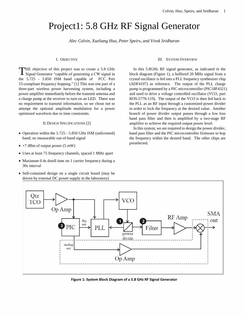
The design of Wilkinson power dividers is covered in
great detail elsewhere [3], and so only the bare essentials are
given here. In the equal split case with a 50 Ω input line, two
¼ λ, 70.71 Ω are required to split the power. A 100 Ω resistor
is connected between the ends of these transmission lines.
The output is matched to 50 Ω. This is illustrated in Figure 6.
Figure 6 The design for a basic equal-split power divider.
Zs in this case is 50 Ω. Figure from [4].
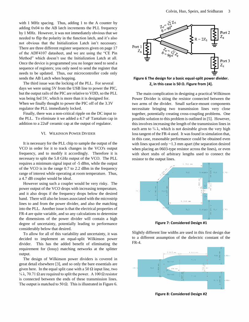
The main complication in designing a practical Wilkinson
Power Divider is siting the resistor connected between the
two arms of the divider. Small surface-mount components
necessitate bringing two transmission lines very close
together, potentially creating cross-coupling problems. One
possible solution to this problem is outlined in [5]. However,
this involves increasing the length of the transmission lines in
each arm to ¾ λ, which is not desirable given the very high
loss tangent of the FR-4 used. It was found in simulation that,
in this case, reasonable performance could be obtained even
with lines spaced only ~1.3 mm apart (the separation desired
when placing an 0603-type resistor across the lines), or even
with short stubs of arbitrary lengths used to connect the
resistor to the output lines.
Figure 7: Considered Design #1
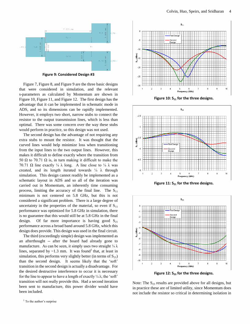
Slightly different line widths are used in this first design due
to a different assumption of the dielectric constant of the
FR-4.
Figure 8: Considered Design #2
Colvin, Huo, Speirs, and Sridharan 4
Figure 9: Considered Design #3
Figure 7, Figure 8, and Figure 9 are the three basic designs
that were considered in simulation, and the relevant
s-parameters as calculated by Momentum are shown in
Figure 10, Figure 11, and Figure 12. The first design has the
advantage that it can be implemented in schematic mode in
ADS, and so its dimensions can be rapidly implemented.
However, it employs two short, narrow stubs to connect the
resistor to the output transmission lines, which is less than
optimal. There was some concern over the way these stubs
would perform in practice, so this design was not used.
The second design has the advantage of not requiring any
extra stubs to mount the resistor. It was thought that the
curved lines would help minimize loss when transitioning
from the input lines to the two output lines. However, this
makes it difficult to define exactly where the transition from
50 Ω to 70.71 Ω is, in turn making it difficult to make the
70.71 Ω line exactly ¼ λ long. A line close to ¼ λ was
created, and its length iterated towards ¼ λ through
simulation. This design cannot readily be implemented as a
schematic layout in ADS and so all of the iteration was
carried out in Momentum, an inherently time consuming
process, limiting the accuracy of the final line. The S11
minimum is not centered on 5.8 GHz, but this is not
considered a significant problem. There is a large degree of
uncertainty in the properties of the material, so even if S11
performance was optimized for 5.8 GHz in simulation, there
is no guarantee that this would still be at 5.8 GHz in the final
design. Of far more importance is having good S21
performance across a broad band around 5.8 GHz, which this
design does provide. This design was used in the final circuit.
The third (exceedingly simple) design was implemented as
an afterthought -- after the board had already gone to
manufacture. As can be seen, it simply uses two straight ¼ λ
lines, separated by ~1.3 mm. It was found1 that, at least in
simulation, this performs very slightly better (in terms of S21)
than the second design. It seems likely that the „soft‟
transition in the second design is actually a disadvantage. For
the desired destructive interference to occur it is necessary
for the line to appear to have a length of exactly ¼ λ; the „soft‟
transition will not really provide this. Had a second iteration
been sent to manufacture, this power divider would have
been included.
1 To the author‟s surprise
Figure 10: S11 for the three designs.
Figure 11: S21 for the three designs.
Figure 12: S23 for the three designs.
Note: The S23 results are provided above for all designs, but
in practice these are of limited utility, since Momentum does
not include the resistor so critical in determining isolation in

Colvin, Huo, Speirs, and Sridharan 5
the simulation. It is assumed that the S23 performance will be
considerably better in practice.
Two copies of the board used for this project were
fabricated -- one to implement the circuit and the other as
backup or for testing. This backup board was cut up to allow
the Wilkinson power divider to be tested in isolation, the
results of which are shown in Figure 13. It was found that the
S21 of the power divider was approximately -3.4 dB at 5.8
GHz and is close to this over a very wide band, much as
predicted by the modeling. It can also be seen that the level of
isolation between the two output ports is much greater than
found in simulation. This is not surprising given that, as
noted earlier, the resistor between the two output lines is not
included in the Momentum simulations.
Figure 13: The measured performance of the power
divider.
VII. BANDPASS FILTER
The specifications for the bandpass filter in project 1 are as
follows
Parameter Specification
Passband 5.725 GHz – 5.850 GHz
Insertion loss targeted <3dB
Out of Band Rejection >30dB
Substrate FR4 (εr = 4.3 +/- 0.5)
For the bandpass filter, the following options were evaluated.
1. Parallel-Coupled λ/2 resonator
2. Lumped Element Filter (with planar elements)
3. Stub bandpass filter
4. End-Coupled λ/2 resonator
The end coupled filter option was eliminated because of
the size occupied, since it is a cascade of half wavelength
segments. Another reason was that FR4, the substrate used
was lossy (tan(D)=0.025). So, the open ended resonators
would cause large substrate losses. The stub bandpass filter
was also eliminated because it is more beneficial for a
wider-band design.[6] Also, the impedance of the stubs were
extremely low at the needed fractional bandwidth (lesser than
10%), leading to very wide stubs.
The other 2 filter options were evaluated. The parallel
coupled filter was designed first. The design parameters for
the 4th order parallel coupled filter are as follows.
g0 1 Resonator Z0e (Ω) Z0o (Ω)
g1 1.5963 1 76.58 38.17
g2 1.0967 2 60.48 42.68
g3 1.5963 3 60.48 42.68
g4 1.0000 4 76.58 38.17
The physical dimensions that were calculated in linecalc and
then optimized for optimal response are as follows.
Figure 14: Parallel Coupled Bandpass Filter
Resonator
Section
Length
(mm)
Width
(mm)
Spacing
(mm)
1, 4 6.5 1.8 0.3
2, 3 6.3 3.8 1.1
Another option evaluated was a lumped element option
(using planar lines). The schematic of the filter is shown
below. R1 and R2 are identical resonators that provide a
passband at 5.78 GHz and the coupling capacitor C2 controls
the bandwidth. L4 and L5 provide transmission zeros for
sharp out-of-band rejection outside the passband.
Figure 15: Schematic of alternate Filter
Colvin, Huo, Speirs, and Sridharan 6
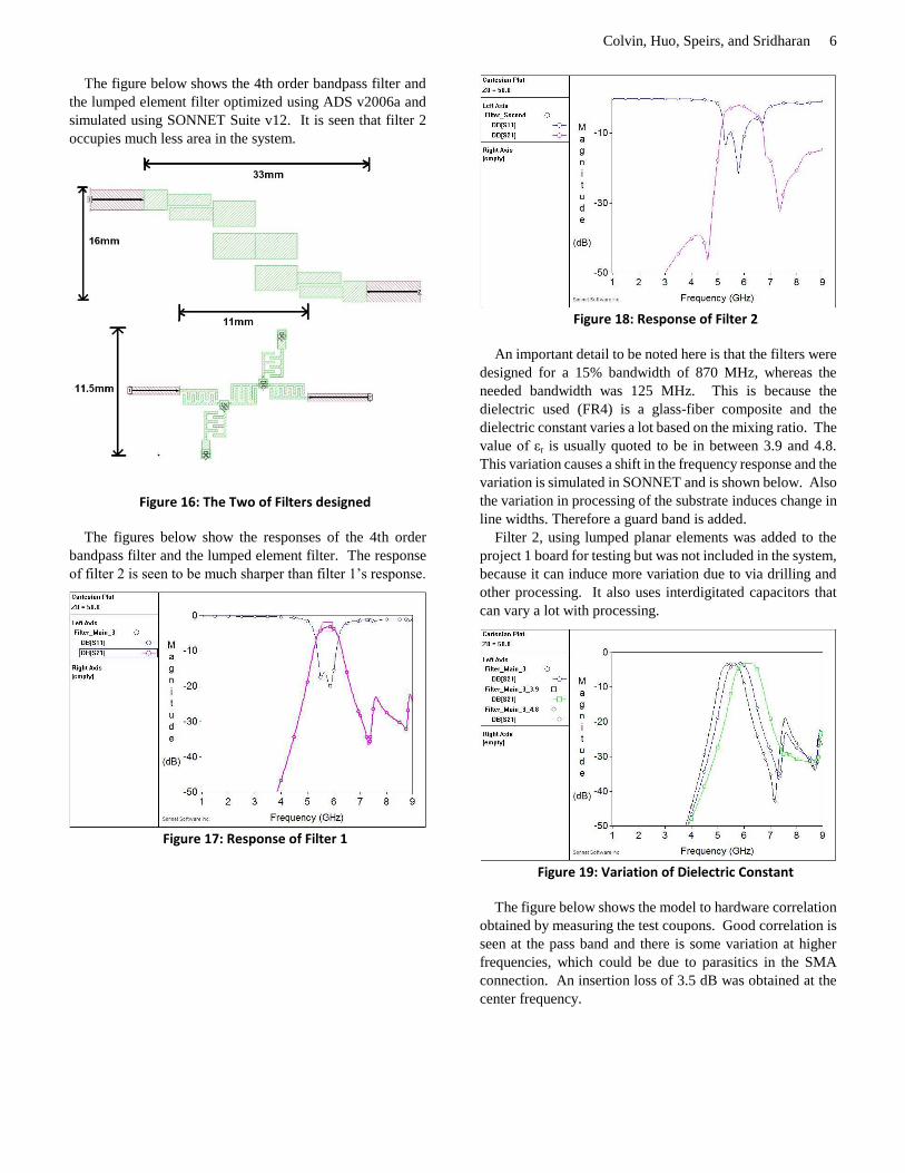
The figure below shows the 4th order bandpass filter and
the lumped element filter optimized using ADS v2006a and
simulated using SONNET Suite v12. It is seen that filter 2
occupies much less area in the system.
Figure 16: The Two of Filters designed
The figures below show the responses of the 4th order
bandpass filter and the lumped element filter. The response
of filter 2 is seen to be much sharper than filter 1‟s response.
Figure 17: Response of Filter 1
Figure 18: Response of Filter 2
An important detail to be noted here is that the filters were
designed for a 15% bandwidth of 870 MHz, whereas the
needed bandwidth was 125 MHz. This is because the
dielectric used (FR4) is a glass-fiber composite and the
dielectric constant varies a lot based on the mixing ratio. The
value of εr is usually quoted to be in between 3.9 and 4.8.
This variation causes a shift in the frequency response and the
variation is simulated in SONNET and is shown below. Also
the variation in processing of the substrate induces change in
line widths. Therefore a guard band is added.
Filter 2, using lumped planar elements was added to the
project 1 board for testing but was not included in the system,
because it can induce more variation due to via drilling and
other processing. It also uses interdigitated capacitors that
can vary a lot with processing.
Figure 19: Variation of Dielectric Constant
The figure below shows the model to hardware correlation
obtained by measuring the test coupons. Good correlation is
seen at the pass band and there is some variation at higher
frequencies, which could be due to parasitics in the SMA
connection. An insertion loss of 3.5 dB was obtained at the
center frequency.
Colvin, Huo, Speirs, and Sridharan 7
Figure 20: Correlation of Measurement and Simulation
VIII. RF AMPLIFIER
The RF amplifier we choose is Gali 39+. We cascaded two
stages to achieve the required 7dBm output power level.
Both amplifiers are biased at 3.5 Vd and 35 mA current. The
schematic of the RF amplifier and its bias circuitry is shown
in Figure 21.
RF Amp
R3
42.5 ohm
+5V
C16
100p
C15
100p
C11
100n
L110uH/RFCU6
Gali39
1IN
3OUT
Figure 21: Schematic of one stage RF amplifier
IX. LAYOUT
PCB layout is important to enable system functional at this
frequency. There are a few layout considerations that we
have implemented in our board.
Solid ground under RF signal path.
Star routing of power supply to minimize the interference
between different function blocks
Keep other components and tracers far away from RF
signal path to avoid interference.
Minimize the bend in RF signal path to avoid loss.
Follow the exact components layout recommended in their
datasheet.
The top layer PCB layout of main circuit board is shown in
Figure 22. Additional layout configurations, the placement of
components as well as bill of material can be found in
appendix.
Figure 22: Top layer PCB layout of signal generator
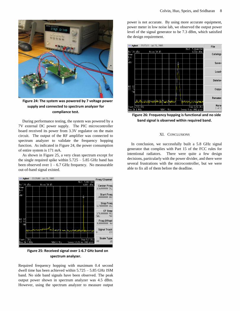
X. RESULTS
The fabricated and populated signal generator PCB board
is shown in Figure 23.
Figure 23: Populated signal generator board connected
with PIC evaluation board.
Colvin, Huo, Speirs, and Sridharan 8
Figure 24: The system was powered by 7 voltage power
supply and connected to spectrum analyzer for
compliance test.
During performance testing, the system was powered by a
7V external DC power supply. The PIC microcontroller
board received its power from 3.3V regulator on the main
circuit. The output of the RF amplifier was connected to
spectrum analyzer to validate the frequency hopping
function. As indicated in Figure 24, the power consumption
of entire system is 171 mA.
As shown in Figure 25, a very clean spectrum except for
the single required spike within 5.725 – 5.85 GHz band has
been observed over 1 – 6.7 GHz frequency. No measurable
out-of-band signal existed.
Figure 25: Received signal over 1-6.7 GHz band on
spectrum analyzer.
Required frequency hopping with maximum 0.4 second
dwell time has been achieved within 5.725 – 5.85 GHz ISM
band. No side band signals have been observed. The peak
output power shown in spectrum analyzer was 4.5 dBm.
However, using the spectrum analyzer to measure output
power is not accurate. By using more accurate equipment,
power meter in low noise lab, we observed the output power
level of the signal generator to be 7.3 dBm, which satisfied
the design requirement.
Figure 26: Frequency hopping is functional and no side
band signal is observed within required band.
XI. CONCLUSIONS
In conclusion, we successfully built a 5.8 GHz signal
generator that complies with Part 15 of the FCC rules for
intentional radiators. There were quite a few design
decisions, particularly with the power divider, and there were
several frustrations with the microcontroller, but we were
able to fix all of them before the deadline.
Colvin, Huo, Speirs, and Sridharan 9
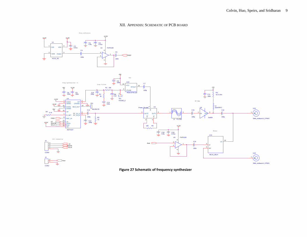
XII. APPENDIX: SCHEMATIC OF PCB BOARD
U15
SMA_endlaunch_CPWG
RF1
U10
SMA_endlaunch_CPWG
RF1
RF Amp
Freq Synthesizer IC
VCO
Loop filter
U5Power_Div ider
IN1
OUT12
OUT23
R1
4
R2
5 L2 FILTER
1 2
R3
42.5 ohm
+5V
U13
ROS-5776-119
VCC14
VTUNE2
RFOUT10
J3
CON4
1234
R6100
C5
100n
+3.3V
C30.01u
C20.01u
Mixer
+3.3V+3.3V
-
+
U2 FHP3130
3
41
52
FREF
C4
100n
C16.8u
C16
100p
C15
100p
Freq reference
J4
CON2
12
C11
100n
PIC connector
U14
MCA1_80LH
IF3
RF5
LO10
L110uH/RFC
U4
ADF4107
R_SET1
CP2
CPGND3
AGND4
RF_IN_B5RF_IN_A6
AVDD7
REF_IN8
VP16
DVDD15
MUX_OUT14
LE13
DATA12
CLK11
CE10
DGND9
SCLKSDATA
LE
LE
SCLKSDATA
FREF
+5V
R45.1k
C9100n
+3.3V
+3.3VC17100p
+5V
C24
100n
C14
100p
C10100p
U6
Gali39
1IN
3OUT
C8100n
C136.8n
C1215pR2
5k
+5V R1 20k
+3.3V
+3.3V
Aout
TP1
VTUNE_0
1
C7
100p
C6100n
TP2
MUXOUT0
1
U1
HC53_XO
E/D1
GND2
Output3
VDD4
R5
51
+3.3V
C190.01u
-
+
U9 FHP3130
3
41
52
C186.8u
Aout
Figure 27 Schematic of frequency synthesizer

Colvin, Huo, Speirs, and Sridharan 10
GND
C2310u
C2222u
C21100n
+5V
+3.3V
U11
LM7805
IN1
OUT3
GND2
C200.33u
Vin
J2
CON2
12
U12 AP1117
GN
D1
Vout
2V
in3
NC
4
TP3
GND
1
D2
LED
D1
LED
+5V
R7330
R8180
+3.3V
Figure 28: Schematic of power management
XIII. REFERENCES
[1] http://www.propagation.gatech.edu/ECE6361/assignme ts/Project1.pdf. Latest access date: June 21, 2009.
[2] Ibid.
[3] D. M. Pozar, Microwave Engineering, 3rd ed. Wiley, 2005.
[4] Stephen Horst, et al., Modified Wilkinson Power Dividers for Millimeter-Wave Integrated Circuits, IEEE Transactions On Microwave Theory and Techniques, Vol. 55,
No. 11, Nov 2007.
[5] Ibid.
[6] Jia-Shen G. Hong, M. J. Lancaster, Microstrip Filters for RF/Microwave Applications, Wiley-Interscience, 2001.