Embed Size (px)
Citation preview

Project Number: RQL-B007
PANSAT POWER SUBSYSTEM
A Major Qualifying Project Plan
submitted to the faculty
of the
WORCESTER POLYTECHNIC INSTITUTE
in partial fulfillment of the requirements for the
BACHELOR OF SCIENCE
By
____________________
Monica Kolb
---------------------------------
Jeffery Meyer
Date: 24 April 2008
Approved:
____________________

2
Executive Summary
The purpose of this major qualifying project (MQP) was to modify the existing
power subsystem design for WPI’s satellite entry in the 2004 competition, NANOSAT-3.
WPI’s entry into the NANOSAT-3 program was the Powder metallurgy And Navigation
SATellite, or PANSAT. This is the fifth team to work on the PANSAT power subsystem, or
PAN-PWR.
The power subsystem is needed to provide regulated power to each of the other
four subsystems on the satellite. In order to do this, the power subsystem must be able to
complete four tasks: collect energy, extract the energy, store the energy and regulate
the energy for the entire satellite. The collection of energy is done by solar cells
mounted on the body of the satellite. From the solar cells, the energy is extracted and
condition via DC-DC converters called Single Ended Primary Inductance Converters,
more commonly know as SEPIC. Energy is stored in an array of batteries, to be used
when the solar cells are unable to provide power for the satellite, such as during the
time of an eclipse. Several secondary DC-DC converters work to regulate the power,
providing voltage rails needed by the other satellite subsystems.
The solar cells used in the NANOSAT-3 contest were the triple-junction GaAs solar
cells manufactured by Space Quest. The cells were configured to make ten separate
panels, two for the top of the satellite and one for each of the eight sides. Based on
MATLAB code for the data on the solar cells, and the orbital parameters given in the
NANOSAT-3 program, the worst case energy collection would be at 87.2 kJ, with the
best case being 229.1 kJ. The approximate efficiency of the power subsystem was
determined to be 81% for all subsystems to operate during the worst case scenario.
For energy storage, each of the solar panels required a separate SEPIC for the
batteries to be charged, resulting in ten SEPICs for the entire satellite. To charge the
batteries efficiently, the energy from the solar cells needs to be combined, so all the
SEPICs are set up in parallel to sum their outputs to the array. The battery array consists
of fourteen Sanyo N-400DRL batteries in series, selected because they were part of the
NANOSAT-3 recommended component list. Initially, the batteries are discharged during
launch, and have to charge before the satellite can begin operations. Once the
output voltage of the batteries reaches around 17 volts, the main computer turns on
along with the other subsystems.
During the operation time of the batteries, it is critical that the voltage not fall
below 16.8 volts; this would be considered a ‘”low power state.” However, the
computer has no way of knowing the charge on across the batteries. A battery charge
tracking and monitoring systems has been designed and prototyped in this project. Its
task is to notify the main computer of the input and output voltage and current running

3
through the battery array. From the numbers provided, the main computer will then
make a decision of whether non-critical systems need to be shut down, until the charge
of the array can be increased again. The Hall Effect sensors used eliminate the need for
an inefficient current sensing resistor, as previous projects had included. Finally, the
sensor data was processed into RS232 output for the main computer to read.
The regulation of energy falls upon the secondary DC-DC converters. With the
fourteen batteries in series, a voltage higher than any individual voltage needed by any
subsystem is provided. With an efficiency of 81% needed by the entire power
subsystem, the step-down switching converters selected by this project have an
efficiency rating ranging from 83% to 96%, depending on the output voltage.
The entire power subsystem has not been tested to measure the efficiency of the
system, so it is unsure whether the rating of 81% overall has been reached. With the work
done so far, any future projects should be able to completely prototype the entire
power subsystem to measure the efficiency and make the design ready to be
successfully implemented on the satellite.

1
Contents
Executive Summary...................................................................................................................... 2
Table of Figures ............................................................................................................................. 3
Index of Tables .............................................................................................................................. 4
Acknowledgements..................................................................................................................... 5
Abstract ......................................................................................................................................... 1
Introduction ................................................................................................................................... 1
PANSAT History........................................................................................................................... 1
Previous Work ............................................................................................................................ 2
Goals for This Year..................................................................................................................... 2
Design Requirements ................................................................................................................... 2
Energy Collection: Solar Panels .............................................................................................. 3
Energy Conversion: Primary SEPICs ........................................................................................ 4
Energy Storage: Battery Array................................................................................................. 6
Energy Conversion: Secondary DC-DC Converters ............................................................ 7
Design Requirement Conclusions .............................................................................................. 9
Project Schedule ........................................................................................................................ 10
Implementation .......................................................................................................................... 12
Battery Status Monitoring....................................................................................................... 12
Input Stage........................................................................................................................... 12
Signal Processing ................................................................................................................. 15
Output Stage ....................................................................................................................... 15
DC-DC Converters.................................................................................................................. 16
Project Progress, Week by Week .......................................................................................... 20
Final Testing and Results............................................................................................................. 25
Conclusion................................................................................................................................... 29
Works Cited ................................................................................................................................. 31
Appendix A. Schematics........................................................................................................... 32
Battery Monitor System, Final Draft....................................................................................... 32

2
DC-DC Converter Schematics.............................................................................................. 34
3.3 V Regulator .................................................................................................................... 34
5.1 V Regulator .................................................................................................................... 35
10 V Regulator ..................................................................................................................... 36
13.8 V Regulator .................................................................................................................. 37
Appendix B. PIC Code in C....................................................................................................... 38
Appendix C. PIC Code in Assembly ........................................................................................ 43
Appendix D. PCB Layouts.......................................................................................................... 60
Battery Monitor Layout........................................................................................................... 60
PCB Layout DC-DC Converters............................................................................................. 61

3
Table of Figures
Figure 1. Side Panel Solar Cell Layout........................................................................................ 3
Figure 2. Top Panel Solar Cell Layout......................................................................................... 3
Figure 3. Top Panel Solar Cell Layout Divided Into Two Panels .............................................. 4
Figure 4. SEPIC Converter from Solar Cells to Battery.............................................................. 4
Figure 5. Ideal SEPIC Converter. ................................................................................................. 5
Figure 6. SEPIC Currents While Switch is Closed (0<t<DT)........................................................ 5
Figure 7. SEPIC Currents While Switch is Open (DT<t<T). ......................................................... 6
Figure 8. Block diagram of battery monitoring system.......................................................... 12
Figure 9. Zetex ZMC20 diagram, from http://www.zetex.com/2.0/pdf/zmc20.pdf.......... 13
Figure 10. Voltage splitter for battery monitor........................................................................ 14
Figure 11. Voltage splitter with low-impedance output for battery monitor. .................... 15
Figure 12: Secondary DC-DC Converter Block Diagram...................................................... 16
Figure 13: Basic Buck Converter ............................................................................................... 17
Figure 14: Current flow in a Buck Converter ........................................................................... 18
Figure 15: Inductor Current in Buck Converter ....................................................................... 18
Figure 16: L4971 Block Diagram................................................................................................ 19
Figure 17: Current Monitor on Breadboard............................................................................. 25
Figure 18: Current Monitor on PCB ........................................................................................... 26
Figure 19: DC-DC Converters on Breadboard ....................................................................... 27
Figure 20: DC-Dc Converter PCB Layout................................................................................. 28
Figure 21: DC-DC Converters on PCB...................................................................................... 29

4
Index of Tables
Table 1. Worst-case and best-case solar panel output power.............................................. 4
Table 2. PANSAT Power Budget. ................................................................................................. 7
Table 3. PAN-TMR Power Specifications. ................................................................................... 8
Table 4. PAN-COM Power Specifications.................................................................................. 8
Table 5. PAN-SEN Power Specifications..................................................................................... 8
Table 6. PAN-NAV Power Specifications. .................................................................................. 8
Table 7: Subsystem Voltage Rails ............................................................................................. 17
Table 8: Resistor values for Regulator....................................................................................... 19

5
Acknowledgements
The team would like to gratefully acknowledge the following people for their help,
advice, and support:
Tom Angelotti, for his unending tolerance with last-minute part orders
Alexander Camilo, for his support both moral and digital
Professor Robert Labonté, for his advice, encouragement, and the occasional prod
Professor Alexander Emanuel, for his support with current-sensing problems
Rory Fuller, for his help in putting together the prototype and holding together the
students
Kevin Harrington, for his advice on all things PIC-related
Professor Susan Jarvis, for her help with elusive PIC bugs
Patrick Morrison, for always knowing where to find that one missing piece of equipment

Abstract
This project has added more functionality to the power subsystem in the PANSAT
satellite project started four years ago. A battery charge tracking system has been
created which will send the satellite main computer a signal recommending that non-
critical systems be powered down during low-power times, such as during an Earth
caused eclipse, or when the battery charge falls too low. Different secondary DC-DC
converters were selected to increase efficiency for the power provided to the different
subsystems of the satellite.
Introduction
PANSAT History
The NANOSAT program is a nanosatellite design and fabrication competition
sponsored by the American Institute of Aeronautics and Astronautics (AIAA), the
National Aeronautics and Space Administration (NASA) and the United States Air Force
(USAF). In total, thirteen colleges and universities across the nation participated in the
event for the chance to design, test, and build a prototype nanosatellite (45 cm in
height and 48 cm diameter). The winning satellite from the University of Texas at Austin
was selected January 9th, 2004 and has since undergone more testing and corrections
with the satellite scheduled to launch in December, 2009. Only the satellite declared
winner was guaranteed to be launched by NASA.
WPI’s entry into the NANOSAT-3 program was the Powder metallurgy And
Navigation SATellite, or PANSAT. The satellite was divided into five subsystems for
development: computer, navigation, sensors, communications and power. The power is
the subject of this paper.
The power subsystem is needed to provide regulated power to each of the other
four subsystems on the satellite. To provide the necessary power, the subsystem must be
able to collect energy via solar panels, extract the energy, store the energy in batteries
and regulate the output of that energy. This must be accomplished under all orbital
conditions the satellite might undergo while in space. Energy is collected in a total of
ten solar cells located on eight sides and the top of the satellite. The extraction of the
energy occurs though ten primary DC-DC converters: the Single Ended Primary
Inductance Converter, or SEPIC. In orbit, the satellite will experience eclipses where no
solar energy can be collected, so some of the energy absorbed by the solar cells is
stored in an array of 14 rechargeable batteries. The batteries will provide power to the
subsystems should the solar cells fail to do so. Finally, regulation of the voltage is

2
accomplished by secondary DC-DC converters, which will provide the voltage rails
needed by the various subsystems.
Previous Work
The power subsystem, or PAN-PWR, has been worked on by four separate senior
design/major qualifying projects, with additional teams possible in the future. Each
team contributed to the current state of the satellite.
The first project, done by Kate Farb-Johnson, determined that the SEPIC was the
most ideal converter to extract energy from the solar cells. Her project, entitled PANSAT
Power Subsystem was complete in D-term of 2004. The second project, done by
Gunnari Auvinen, Tiffany Tam, and Bandar Turkmani, developed a control circuitry for
the SEPIC. This project, entitled Control Loop for the PANSAT Power Subsystem, was
completed E-term of 2004. In D-term of 2005, Brandon Gillet, Paul Messier and Christian
Shetler worked on designing and building a fully functional prototype of the power
subsystem, and the previous two projects had not. Their project was also entitled
PANSAT Power Subsystem. Finally, completed in D-term 2006, Joseph Citro, Kurt Ferreira
and Melissa Marion re-examined the 2005 project in order to increase the efficiency of
the SEPIC up to working standards and were successful in their task.
Goals for This Year
The goals for this year included implementing a battery charge tracking system,
which would send the main computer current and voltage readings from the battery.
The main computer would then decide to shut down non-critical systems in case of low
power. With the primary SEPIC efficiency increased, the secondary DC-DC converters
were re-evaluated in order to increase their efficiency as well. These goals were formed
with the intent to increase the all around functionality of the PANSAT power subsystem.
In this report, the design requirements of the satellite are explained in Section X;
this includes the energy collection, conversion and storage details. The next section,
Section X, details the work done this year for the battery monitoring portion of the
project. Section X explains what was done to improve the secondary DC-DC
converters.
Design Requirements
The PANSAT power subsystem consists of several distinct stages: energy
collection, storage, and transfer. Energy conversion occurs between collection and

3
storage and again during transfer. In this section we examine each stage of the power
subsystem and discuss the requirements for each part.
Energy Collection: Solar Panels
The PANSAT project has been developed with Space Quest triple-junction GaAs
solar cells (Gillet, Messier, & Shetler, 2005, p. 13). These cells are placed in panels on
each of PANSAT’s eight sides; an additional two panels are placed on top of the
satellite.
Figure 1. Side Panel Solar Cell Layout (Citro, Ferreira, & Marion, 2006, p. 38)
Figure 2. Top Panel Solar Cell Layout (Citro, Ferreira, & Marion, 2006, p. 38)

4
Figure 3. Top Panel Solar Cell Layout Divided Into Two Panels (Citro, Ferreira, & Marion, 2006, p. 38)
The top panels each give 2.1V*19 = 39.9 V at peak power; each side panel gives
2.1V*24 = 50.4 V at peak power (Citro, Ferreira, & Marion, 2006, p. 37).
The following table indicates the worst-case and best-case power output of the
solar panels (Gillet, Messier, & Shetler, 2005, p. 13):
Worst Case (W) Best Case (W)
Per Side Panel 13 18
Per Top Panel 4.5 11.5 Table 1. Worst-case and best-case solar panel output power.
Energy Conversion: Primary SEPICs
Figure 4. SEPIC Converter from Solar Cells to Battery. (Farb-Johnson, 2004, p. iii)
The challenge of extracting power from the solar panels comes when it is time to
combine the outputs. These solar panels act as voltage sources. It is unsafe to combine
them directly in parallel, and combining them in series severely limits the amount of
current that can flow through them. For this reason, each solar panel must have its

5
output converted to a current source. Then a parallel combination will add each
panel’s current together.
The converter that performs this in the PANSAT power subsystem Is known as a
single-ended primary inductance converter, or SEPIC. This DC-DC converter draws
continuous current from its source and presents a positive current source to its load.
The ideal SEPIC converter is shown in Figure 5. When the controlling switch is off,
power flows through Ls and charges Cc. This causes current to flow through L1,
charging Cout and powering Rl. When the switch is turned on, Cout discharges through
Rl while D prevents current from leaking back to the source.
Figure 5. Ideal SEPIC Converter. (Farb-Johnson, 2004, p. 3.15)
Figure 6. SEPIC Currents While Switch is Closed (0<t<DT). (Farb-Johnson, 2004, p. 3.15)

6
Figure 7. SEPIC Currents While Switch is Open (DT<t<T). (Farb-Johnson, 2004, p. 3.15)
A previous project implemented a peak power tracking system that monitored
the output current from each SEPIC and controlled the duty cycle to maximize power
output. That now forms the control system for the SEPIC switches.
Energy Storage: Battery Array
The battery array consists of fourteen Sanyo N-4000DRL batteries connected in
series (Citro, Ferreira, & Marion, 2006, p. 3). These batteries charge to an initial value of
19 V before first turning on the computer, PAN-TMR; they can be charged further up to
20.1 V (Citro, Ferreira, & Marion, 2006, p. 32).
How much energy does the battery need to store? Previous projects have
established the power budget shown in Table 2. This budget governs all the satellite’s
energy use.
Computer: Low Power
Computer: Norm Power
Sensor Sweep
Transmitting Unit Total
Max Min
PAN-TMR 6.505 2.2154 2.2154 6.505 6.505 6.505 W
PAN-COM 7.242 4.77464 4.77464 4.77464 4.77464 7.24222 W
PAN-SEN 7.2155 0 0 0 7.2155 0 W
Power Usage
9.89004 14.171964 21.39514 16.64722 W
Time/State Filler Activity
900 20 1350 s
State Qty Filler Activity
1 9 1 #

7
Time 3170 900 180 1350 s 5600
Energy 31351.4 12761.7 3851.1 22473.7 J 70437.9
Qty/Light Phase
Filler Activity
1 4 0 #
Time/Light Phase
1820 900 80 0 s 2800
Energy/Light Phase
17999.9 12761.7 1711.6 0 J 32473.2
Qty/Dark Phase
Filler Activity
0 5 1 #
Time/Dark Phase
1350 0 100 1350 s 2800
Energy/Dark Phase
13351.5 0 2139.5 22473.7 J 37964.7
Table 2. PANSAT Power Budget.
(Gillet, Messier, & Shetler, 2005, p. 34)
It is prudent to be aware of the charge state of the battery for two reasons: to
avoid overcharging and to prevent critical power loss. In the first case, a monitoring
system could send a signal to switch off some of the charging SEPICs if the batteries are
in danger of overcharging. In the second case, a low-power warning should be sent to
PAN-TMR so that it can shut down noncritical systems before power fails. This battery
monitoring has not been implemented in previous projects.
Circuitry for monitoring the current output of each SEPIC was implemented in
Gillet, Messier, and Shetler’s 2005 project. The SEPIC current is sent through a 0.5 Ohm
resistor, and the resulting voltage is read and interpreted by the PIC processors that the
MQP team used for peak power tracking (Gillet, Messier, & Shetler, 2005, pp. 50, 57). This
project can also use this data to see how much current is flowing into the batteries.
Previous designs included no means of monitoring the current output through the
secondary DC-DC converters. Some such monitor should be implemented in some way
that minimizes power loss.
Energy Conversion: Secondary DC-DC Converters
The combination of solar panels and battery power all the subsystems of the
satellite. Each subsystem runs off several voltage rails with different requirements. These
requirements are summarized in Table 3 through Table 6.
The following tables, copied from Gillet, Messier, and Shetler’s 2005 report (pp.
32-33), show the power specifications for PANSAT’s subsystems.
Voltage Rail (V) Low Power Mode (mA) Normal Mode (mA)
3.3 264 750

8
3.3 264 750
5 86 311
Power (W) 2.2154 6.505 Table 3. PAN-TMR Power Specifications.
Voltage Rail (V) Beacon Mode 1 (mA)
Beacon Mode 2 (mA)
Transmit Mode (mA)
13.8 160 160 160
13.8 0 0 164
13.8 120 120 120
13.8 0.1 0.1 0.1
5 0.8 0.8 0.8
3 29 29 29
Transmitting Power (W)
0 1 1
Total Power (W) 3.956 4.956 7.242 Table 4. PAN-COM Power Specifications.
Voltage Rail (V) PAN-SEN Average (mA)
PAN-SEN Max (mA)
Temperature Sensors (mA)
Hall Effect Sensors (mA)
5 689.8 1080.1 - 55
10 212 144.4 9.6 -
Power (W) 5.569 6.8445 0.096 0.275 Table 5. PAN-SEN Power Specifications.
Voltage Rail (V) Normal Mode (mA)
5 160
5 160
5 160
5 160
Power (W) 2.9 Table 6. PAN-NAV Power Specifications.
(Gillet, Messier, & Shetler, 2005, pp. 32-33)
Previous projects worked with a quick sketch of the secondary DC-DC converters
using the LM2676T family in its adjustable, 6V, and 3.3V forms (Gillet, Messier, & Shetler,
2005, pp. 51-55). A single converter was used for each voltage rail required. This project
will more closely examine the secondary DC-DC converters in an attempt to select an
appropriate, high-efficiency chip.

9
Design Requirement Conclusions
Several parts of the power subsystem have been critically evaluated and tested
already. The solar panels and primary DC-DC converters may require no additional
modification. However, the current solar panel setup requires that our power subsystem
achieve 82% efficiency (Citro, Ferreira, & Marion, 2006). Within this constraint, this
project must design efficient secondary DC-DC converters to meet several voltage rail
requirements.
The other major goal of this project is to implement a battery charge-tracking system so
that PANSAT can shut down noncritical systems in case of low power during eclipse or,
alternatively, shut down SEPICs to avoid overcharge during the light phase. Any power
loss from this tracking affects overall subsystem efficiency.

10
Project Schedule
The project is scheduled to run through term C08. This requires a compact,
seven-week schedule, summarized below.

11

12
Implementation
Battery Status Monitoring
It was decided early in the project that most processing involving the battery
measurements should be done by the main satellite computer. This computer is triply
redundant and has already been designed for the rigors of space. However, for a
demonstration of this project, some minimal processing was required. We decided to
monitor the current running into the battery, the current running out, and the voltage
across the battery terminals.
A PIC16F874A was selected as a familiar base to work on. Three channels of its
A/D converter were assigned to convert the battery’s input current, output current, and
voltage level. Finally, its Universal Asynchronous Receiver/Transmitter (UART) was used to
transmit battery information through a level converter to RS232, which could then be
read by a host computer.
The processing for the battery status monitor is summarized in the block diagram
below.
Figure 8. Block diagram of battery monitoring system.
Input Stage
The first attempt at monitoring current used the Zetex ZMC20 current sensor, rated for
currents up to 20A. It works with a set of four magnetoresistors, laid out as shown in
Figure.

13
Figure 9. Zetex ZMC20 diagram, from http://www.zetex.com/2.0/pdf/zmc20.pdf
In theory, the magnetic field induced by flowing current alters the resistances of
the four magnetoresistors; the distance between the resistors and the conductor
determines the magnitude of this alteration. However, when a simple circuit was set up
to test this, the ZMC20 gave negligible voltage output through multiple attempts and
with multiple chips. Eventually we abandoned it in favor of a different solution.
The second attempt at monitoring current was designed to get rough voltage
estimates in order to test the PIC code. It used two power resistors of 0.1 Ohms, one on
the battery current input, one on the current output.
The current-sensing resistor approach has one critical drawback: power loss. The
power dissipated in a resistor is equal to RI2. Power resistors are not often available for
resistances below 0.1 Ohms, leading to a power loss of 0.1 times the square of the
current running through it. The losses of a transformer are considerably lower, but the
dual-coil transformer requires AC current. There exists a more efficient way to determine
DC current: the Hall effect.
When an electrical current runs through a conductor, it induces a magnetic field
perpendicular to the flow of current. This field, in turn, exerts a force on the moving
charge carriers, pushing them towards one side of the conductor and leaving a
shortage of carriers on the other side of the conductor. Therefore, a voltage
accumulates on opposite faces of the conductor. This voltage is proportional to the
magnitude of the current: more current causes a stronger magnetic field and more
deflection, and less current causes a weaker magnetic field, allowing charge carriers to

14
stay closer to a straight path through the conductor. A Hall effect sensor takes this
voltage and makes it available to an outside observer without interfering with the main
flow of current.
Many Hall effect sensors are made for low-current applications. The Allegro
Microsystems ACS713ELCTR-20A-T permits readings of up to 20A on a 5V power supply,
making it ideal for our application. Initial testing indicated that it gave useful voltage
readings directly to the PIC without the need for signal scaling.
The battery voltage could vary from 16.8 to 20.1V, and so we chose to scale it
down by a factor of slightly more than four in order to get a signal input compatible
with our 5V A/D converter. Therefore, a simple voltage divider was used, as illustrated in
Figure 10.
Figure 10. Voltage splitter for battery monitor.
After testing, it was discovered that the A/D converters required low-impedance
inputs. The current sensor could send its data straight into the A/D converter. The
voltage splitter for the battery required an op-amp to buffer it. A non-inverting op-amp
with a gain just over 1 was selected, as shown in Figure 11.

15
Figure 11. Voltage splitter with low-impedance output for battery monitor.
Signal Processing
Minimal processing was required to use the values obtained from the input
sensors. In order to get an output that could be tested, the inputs were taken by the PIC
and stored in three different variables. Then, one by one, each variable was converted
to an ASCII representation of itself and output to the UART.
Output Stage
The UART output data in the RS232 signal format, but at voltage levels from 0 to
5V instead of the RS232’s -13 to 13V. A MAX232 converter chip was used to convert this
voltage level, after which the output data could be connected to pin 2 of a serial
cable and read by a terminal emulator on any host computer.
The settings for the serial connection were determined based on simplicity. 9600
baud was determined to be fast enough to give useful information, but slow enough to
avoid the problems of extremely high-frequency signals. The data used the common
settings of 8 bits to a byte, one stop bit, and no parity bit.

16
DC-DC Converters
In order for the entirety of the satellite to operate, several different voltage rails
were necessary to provide energy for different subsystems of the satellite. Rather than
installing separate batteries for each of the voltage rails, the more realistic option of
implementing DC-DC converters was chosen. A DC-to-DC converter is a device that
accepts a DC input voltage and produces a DC output voltage. Utilizing DC-DC
converters allows for one voltage source to power several systems that require different
voltage rails. For the PANSAT, there are four subsystems that require voltage rails that
differ from what the battery provides: the onboard computer (PAN-TMR), the
communications system (PAN-COM), the sensors (PAN-SEN), and the navigation system
(PAN-NAV). Referenced from the Design Requirements section, the chip necessary for
the conversion would need to be able to output 3, 3.3, 5, 10, and 13.8 volts. The
following block diagram, Figure 12, shows an overview of the requirements.
Figure 12: Secondary DC-DC Converter Block Diagram

17
Several of the subsystems require multiple voltage rails rather that a single one.
Table 7 below shows the voltage rails needed by each of the satellite subsystems1.
Table 7: Subsystem Voltage Rails
Voltage Rail
(V)
PAN-TMR PAN-
COM
PAN-
SEN
PAN-
NAV
3 X
3.3 X
5 X X X X
10 X
13.8 X
None of the voltage rails required by the satellite subsystems exceeds the
voltage provided from the batteries, so the type of DC-DC converter chosen was a step
down, or buck, converter. The circuit diagram for a basic buck converter is shown
below in Figure 13.
Figure 13: Basic Buck Converter
A buck converter is in the family of switching regulators,2 which employ the use
of a capacitor, inductor and a diode along with a pulse-width modulator (PWM), which
is generally a transistor. The PWM controls the duty cycle, or ratio of the time the switch
is on versus the total time in one period (ton + toff), of the circuit. When the switch is on,
current will flow through the inductor and charge the capacitor. Once the switch
closes, the input voltage to the inductor is removed; however, the current in an inductor
cannot fall to zero instantaneously, so the inductor voltage falls to keep the current
steady. The equation for a voltage across an inductor is depicted below.
1 Based off of Design Requirements section
2 Switching regulators include buck, boost, buck-boost, and flyback converters.

18
VL = L di/dt 1
Once the inductor voltage falls far enough, the diode, which was previously
reverse biased and consequently off, becomes forward biased?, allowing current to
flow through the diode and load. During the off time, the capacitor is also discharging
through the load. Figures X and Y below illustrate the behavior of the circuit and how
the current through the inductor reacts to the switching.
Figure 14: Current flow in a Buck Converter
Figure 15: Inductor Current in Buck Converter
The duty cycle for Figure 15 would be:
D = Ton/(Ton + Toff) 2
The output voltage, Vo, is dependant on the input voltage, Vs, and the duty
cycle, D:
Vo = VsD 3
In selecting a converter for this project, a converter with a robust PWM controller
was a necessity. The chip decided on was the L4971 step down switching regulator
from ST Microelectronics. This chip was able to output four of the five required voltage
rails, with 3 V being the only rail unobtainable. The L4971 regulator was chosen for a
number of reasons. First, it allows a variable input, ranging from 8 to 55 volts, and a max
current output of 1.5 amps. The input voltage range from the batteries was from 16.8 to
20.1 volts, falling well within the limits of the regulator. Also, none of the subsystems
require more than 1.5 amps from a single regulator. Second, the regulator allowed for a
variable output. Two resistors’ values could be changed to output any voltage rail from
3.3 to 50 volts. Finally, with the block diagram provided in the datasheet illustrating
exactly how to build the regulator, finding the necessary resistors, capacitors and
19
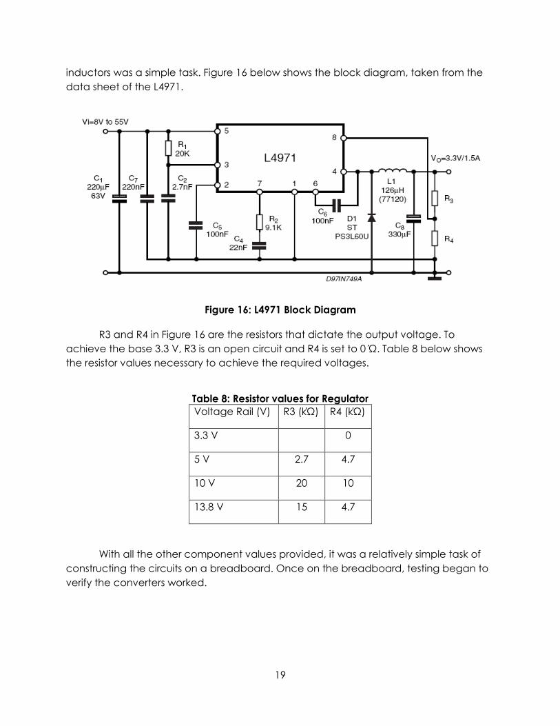
inductors was a simple task. Figure 16 below shows the block diagram, taken from the
data sheet of the L4971.
Figure 16: L4971 Block Diagram
R3 and R4 in Figure 16 are the resistors that dictate the output voltage. To
achieve the base 3.3 V, R3 is an open circuit and R4 is set to 0 Ώ. Table 8 below shows
the resistor values necessary to achieve the required voltages.
Table 8: Resistor values for Regulator
Voltage Rail (V) R3 (kΏ) R4 (kΏ)
3.3 V 0
5 V 2.7 4.7
10 V 20 10
13.8 V 15 4.7
With all the other component values provided, it was a relatively simple task of
constructing the circuits on a breadboard. Once on the breadboard, testing began to
verify the converters worked.

20
Project Progress, Week by Week
Week 1: 18 January 2008
The project schedule for this week called for the simulation and selection of a
topology for the PANSAT subsystems' DC-DC converters. It also called for research on
the parts required for these converters, the layout of the SEPICs to be replicated and
tested, and the beginning of research on the parts for the battery monitors.
The team decided early in the week to find a ready-made, space-qualified DC-DC
converter. This proved more difficult than first expected. Earlier projects had modeled
off the LM7378 series of converters, but this line has no equivalent on the QML Class V list
for space-qualified parts. A search was conducted through the manufacturers listed in
NASA's Qualified Parts List Directory. The vast majority of these manufacturers only made
high-performance relays and interconnects. A smaller subset made sensors or metal-foil
resistors. Only Texas Instruments appeared to have QML-V qualified DC-DC converters.
An independent search also showed that International Rectifiers produced some
space-qualified converters.
Many of these converters had very low current capabilities; most TI families could only
handle 0.5 A DC. This was insufficient for several of PANSAT’s subsystems. A search of the
TI parts that qualified, the TI parts that would work for some subsystems, and the
International Rectifier parts that qualified showed that none of these parts were
available for online ordering. Eventually the team found one item in the same family as
a qualified TI part: the UC1823, through Arrow. However, the listed lead time for that
was eight weeks, making it impractical for the timeframe of our project. An equivalent
or similar DC-DC converter was sought for the prototype; an item similar to the QML-V
certified ones, but made to commercial specifications, should be available much
faster. The team ordered samples of TI's UC3823, which should perform in a similar
manner to the UC1823.
The team did obtain the SEPIC schematics from the 2006 MQP. This includes test
points for battery monitoring. Plans were made to obtain a prototype from a previous
team in order to use an actual SEPIC setup as the input to the battery-charging system.
The battery monitoring consists of current monitoring into and out of the battery and
voltage monitoring on the battery terminals. The 2006 MQP team that added peak
power tracking to the subsystems had already placed current and voltage monitor
points at the output of each SEPIC, and fed these into a PIC microprocessor. This project
will need to add another current monitor at the battery output with a minimum of
power loss. Then it must be determined what kind of algorithm and error-checking will
lead to accurate charge monitoring on the battery.
In conclusion, the team found that it will take more research and some compromise
to locate parts that will arrive on time. It was decided not to simulate converter

21
topologies from scratch. In the next week the team expects to locate an acceptable
DC-DC converter and order it. The team also hopes to review the SEPICs of previous
projects and either order parts for one or obtain an old prototype from a previous team.
Finally, the design of the battery monitor will be finalized and the monitoring code will
be outlined.
Week 2: 24 January 2008
This week the project called for a finalization of the DC-DC converter, battery monitor,
and SEPIC prototype parts lists. The team also planned to have an initial parts order
submitted on Tuesday, January 22. Finally, the team had hoped to begin writing the
code for the battery monitor.
For the DC-DC converters a commercially available part was found, the ST
Microelectronics L4971. This is an adjustable converter that can handle up to 1.5 A of
output current. It is adjustable from 3.3V to 50V, making it suitable for four of our five
voltage rails. The fifth voltage level, 3V, will be achieved with a custom-built buck
converter. Initial simulations indicated that a 270 uH inductor would be appropriate,
along with a Schottky diode that allowed up to 24V reverse voltage. The least
expensive commercial axial-lead diode we found for this was the Discrete
Semiconductor 1N5822G. These parts will be used for the prototype. An initial parts list
was sketched and all parts not available on hand were ordered.
The battery monitor's hardware had to consist of two current monitors: one at the SEPIC
output, and one at the battery output. The team found relatively few current sensors
that specified they could accurately measure DC current; the Zetex ZMC20 was chosen
for this task, and two of them were ordered.
Finally, it was determined that it was not necessary to build another SEPIC prototype.
This project focuses on the battery monitor, so a power supply will be used to simulate
the SEPIC output in initial testing.
The battery monitor code must evaluate the current going into and out of the battery
monitor. It must integrate these values over time to determine the charge currently in
the battery. This approach is likely to accumulate error over time; the monitor should
also keep track of the battery voltage as a sanity check, and adjust the estimated
charge if the battery voltage is higher or lower than expected.
A flow chart to indicate this code was drawn up, and the processor, a PIC16F874, was

22
selected. The team hopes to write the code in C, but has not yet located a C compiler
for the PIC16F series. A pseudocode program can be broken down to assembly code if
necessary.
All hardware for the PIC setup is already on hand.
Both hardware orders have been placed at this time, and the team hopes to have
them next Wednesday, January 30. Jeff will be responsible for planning the analog
hardware setup, and Monica will concentrate on writing and testing code for the
battery monitor.
Week 3: 31 January 2008
This week the project called for programming the bulk of the battery monitor and
building the DC-DC converters.
The battery monitor is run by a PIC16F874A. The code was written in C and compiled by
the SourceBoost compiler. From there, Microchip's MPLAB assembled the code. A
simple code loop was written at first: check the system time, check the current coming
into the battery and the current coming out of the battery, calculate the net current,
check the system time, multiply current by time to get battery charge. This code will
later be modified to check the battery voltage and update the expected battery
charge if the voltage is out of normal bounds. The code must also give some part of this
data - either all data, or just flags on error conditions - to the main computer.
The first draft of the code was loaded onto a PIC, but the processor appeared to be
inoperative. A new oscillator has been obtained, and a second PIC has been located
should it become necessary to replace the first one. More troubleshooting will be done
Thursday and Friday in the hopes of getting the basic code working.
Of the six necessary DC-DC converters, schematics for five of them have been drawn
up and finalized. Using the L4971 DC-DC Converter from STMicroelectronics, the
converters were configured to provide the 3.3, 5, 10, 13 and 13.8 V outputs necessary
for the PAN-TMR, PAN-COM, PAN-SEN and PAN-NAV. The only voltage level not yet
achieved is the 3 volts for the PAN-COM. The schematic for the 3 V DC-DC converter
has been drawn up, however there are currently problems interpreting the data sheets
for the TI UC3843N Pulses Width Modulation controller. The PWM controller is required
because the input voltage from battery can vary from around 18 to 20.1 V. this variation
would cause fluctuations in the output of the DC-DC converter to vary as well. The PWM
controller will correct the duty cycle of the MOSFET switch of the converter to hopefully

23
adjust to output a constant 3 V, with input variations. If the team cannot determine how
to correctly incorporate the PWM controller, we will try to find a replacement or build
our own.
The DC-DC converters will be added onto a protoboard and tested within the next few
days to verify the calculations and that they work correctly.
By next Thursday it is hoped to have a working PIC with our battery monitor code. The
plan also calls for building the battery monitor and testing it with some kind of readout,
possibly a row of LEDs to indicate percent charge. The Sanyo N-4000DRL batteries from
previous projects have not been located; a rush order may be necessary. Finally, all
DC-DC subsystem converters should be assembled with their efficiency measured
through multiple runs.
Week 4: 5 February 2008
Since this past Thursday the PIC has been repaired, with the timer functioning so that
charge can be monitored if we know the changing current. From here it is only
necessary to get the A/D converters working to interpret the current monitors' input,
then implement sanity checks based on the battery voltage, then decide which
conditions to tell the main computer about.
Week 5: 11 February 2008
At this point the project has moved from design into building and testing.
The battery monitor only requires calibration with the zero point and full-charge point of
the battery array. It can currently take voltage representing the current into the battery,
integrate this over time, and thus maintain a number representing the charge present in
the battery. A small modification will add a second input so that the monitor can track
input and output current. Finally, voltage monitoring will be added as a sanity check, so
that the estimated charge is set to minimum if the voltage drops too low.
Battery monitor development was slowed a little by the accidental destruction of the
first PIC processor, due to misalignment in the programming circuit. It was further slowed
by the fact that the current-monitoring sensors, the Zetex ZMC20s, did not appear to
work - all test setups resulted in meaninglessly small output voltages. Several setups
have been investigated, and a few more possible setups will be tested. If that does not
work, a new sensor will be obtained. Once a current sensor is working, the monitor can
be calibrated to keep the expected charge value within the appropriate variable size.

24
The DC-DC converters are giving quite a lot of problems. All parts have been obtained
and work has been focused on building one correctly and verifying the it does indeed
work correctly. However, the circuit is proving more difficult to construct then previously
assumed. This has to do with the fact that a few of the capacitors on the schematic
from the data sheet do not have an orientation list for positive and negative pins.
However, once the issues have been worked out, the remaining four converters will be
built quickly. From there, the custom DC-DC converter will be finalized and constructed.
Week 6: 25 February 2008
This past week was devoted to testing and troubleshooting the project circuit. This was
done in two major sections: the battery monitoring circuit and the DC-DC converter
stage.
The battery array from previous projects was recovered and rebuilt this week. The
fourteen Sanyo N-4000DRL batteries were in a sturdy battery case, but the connections
were weak and many were broken. These connections were re-soldered so that the
battery array is ready to be put in a test circuit.
The battery monitor has already demonstrated counting charge. This week, voltage
monitoring was added and calibrated such that the PIC will output a warning flag if the
battery drops below 16.8V, or a different warning flag if the battery charges above
20.1V. For the moment, the accuracy of the calculated current and charge limits are
unknown; over the coming week, the team will test charging and discharging the
batteries through this actual monitoring circuit in the hopes of making the current-
monitored charge count line up with the voltage-monitored status.
The current monitor was tested using a resistor rather than a Hall effect sensor. There is
not enough time left in the term to obtain and test a new Hall effect sensor, but during
D term we hope to get a working Hall effect sensor, as this will improve overall
efficiency.
The DC-DC converters are still giving a bit of trouble. The converter outputting 3.3 V (the
base value for the converter) is working correctly and outputs 3.3 V with a varying input
voltage. The four others that require resistors to alter the output voltage are not quite
working. We have one outputting a voltage between 8.5 to 9 V. Once the problem with
the converter is located and fixed, implementing the remaining converters will not be a
difficult task. During last week's meeting, it was suggested that we purchase resistors
with a higher power rating, however, we have utilized the same resistors as before, so

25
the higher power rated resistors may not be necessary.
At the end of this week, the plan calls for an assembled prototype: from an input
current source, current will flow through a monitoring resistor to the battery. Current will
then flow out through another monitoring resistor to a rail from which DC-DC converters
can draw their current. A working demonstration will take the base current source and
provide our five voltage rails on the DC-DC converter outputs. It will also indicate when
the battery charge or voltage drops too low; this indication may be connected to a
simpler demonstration circuit in order to prevent having to charge and discharge
fourteen 4000mAh batteries for every test cycle.
Final Testing and Results
Once the code was written, the current monitor was ready to be tested. At first, it
was constructed on temporary breadboard. Figure 17 below shows the monitor on
breadboard.
Figure 17: Current Monitor on Breadboard

26
After thorough testing on the breadboard, a PCB layout was designed and
ordered. Once the board arrived, all the components were soldered on and were
testing again. Figure 18 below shows the PCB layout with components added.
Figure 18: Current Monitor on PCB
The board did not work correctly. The PIC was replaced with a spare and
retested, which did not work. The code was re-examined and tested again on the
breadboard. After fixing a few problems that were discovered and with the PIC work on
the breadboard, testing was done on the PCB, once again. Eventually it was
determined that the A/D converters on the PIC required a low-impedance input. This
had been inadvertently set up on the breadboards but had not been designed into the
PCB. As a result, the current monitor is still prototyped on the breadboard. A simple op-
amp buffer is all that was required to offer a low-impedance input to the A/D
converters. The MultiSim schematics have been adjusted to correct the faults, however,
due to time constraints, the PCB will not be re-ordered.

27
As soon as the parts for the DC-DC converters arrived, construction and testing
began immediately. The schematic for each converter is shown in Appendix A.
Thorough testing was done, and after rebuilding the converters a number of times,
each outputs the correct respective voltage rail. Figure 19 displays a photograph of the
four regulators laid out on a large breadboard.
Figure 19: DC-DC Converters on Breadboard For the prescribed voltage range (17.0 to 20.1 V) the four regulators output the
appropriate voltage for the circuit configuration. However, while on the breadboard,
the regulators demonstrated some strange behaviors. While the 3.3 and the 5 V
regulators work perfectly over the tested voltage range (8 to 25 volts), the 10 and 13.8 V
regulators did not operate quite as ideally. If the input voltage to the regulators
dropped below 15 volts, both of the regulators’ outputs dipped to around 8.4 volts and
would not recover from that state. The only method to correct this error was to turn off
power to the regulators and then reapply it, with the voltage level above 15 volts.
However, this behavior should not be a large problem because the voltage level will
not drop below 16.8 V; 16.8 V would be considered to be a low power state, and non-
critical systems would be shut down until the batteries can be charged back up.

28
Once the converters were successfully built on the breadboard, a PCB layout
was created. The schematics for the converters were created in MultiSim, shown in
Appendix A, and then exported to Ultiboard. Figure 20 below show the layout of the
PCB in Ultiboard, taken from Appendix B:
Figure 20: DC-Dc Converter PCB Layout
On each board are two DC-DC converters, so two boards had to be ordered.
The large rectangular shapes are the custom footprint for the inductors, while the
smaller rectangles are either capacitors or resistors. The square-shaped footprints
represent the binding posts to be added onto the board: one for power, one for
ground and one for each converter output. Figure X below shows a photograph of the
complete PCB with components soldered on.

29
Figure 21: DC-DC Converters on PCB
Like the current monitor, the PCB does not work correctly for the DC-DC
converters either. Both the 3.3 V and 5 V converters are outputting around 9.2 V. Like
the current monitor, the PCB will not be re-ordered and constructed due to time
constraints.
Conclusion
The goals for this year’s project were to implement as battery charge tracking
system and to increase the efficiency of the secondary DC-DC converters. These goals
were achieve through careful component selection and through rigorous testing. All
sections of the project currently are working on breadboard.
After thorough testing of the final designs, and based off the efficiency ratings for
the DC-DC converters from the data sheet, the project was a success. There still are a
few issues, concerning the PANSAT power subsystem as a whole, which should be
examined before any actual implementation is done.
While the current monitor is working on the breadboard, a printed circuit board
was ordered, but the PCB did not work correctly. As a result, the current monitor is still
prototyped on the temporary breadboards. The schematics in Multisim have been
adjusted to rectify the problems, but will not be re-ordered due to the lack of remaining
time. The entire monitoring system, including Hall Effect sensors, voltage monitors, and
serial output of this data, was successfully built on the breadboard. Should any
subsequent project choose to implement this in a final design for the power subsystem,
fabricating the PCB should not be a problem.

30
The secondary DC-DC converters are also working on the breadboard. A PCB
was fabricated for the converters, but failed to work correctly and will not be rebuilt.
The datasheet for the L4971 regulator states that the efficiency of the converters should
be between 83% and 96%, however this has not been tested. As stated, the efficiency
of the entire power subsystem must be at least 81% and if all of the converters
implemented in this project do not achieve that efficiency, they must be redesigned.
Finally, the entire power subsystem has not been completely built and tested,
with all sections included in the final prototype. It would behoove a future team to
construct the power subsystem to verify all work done by this and previous projects.

31
Works Cited
Citro, J., Ferreira, K., & Marion, M. (2006). PANSAT Power Subsystem. Worcester:
Worcester Polytechnic Institute.
DC-DC Converter Tutorial, Maxim IC, Created Nov 29, 2001
http://www.maxim-ic.com/appnotes.cfm/appnote_number/2031/
Farb-Johnson, K. E. (2004). PANSAT Power Subsystem. Worcester: Worcester Polytechnic
Institute.
Gillet, B., Messier, P. F., & Shetler, C. (2005). PANSAT Power Subsystem. Worcester:
Worcester Polytechnic Institute.
Ledwich, G. (1998), DC-DC Converter Basics,
http://www.powerdesigners.com/InfoWeb/design_center/articles/DC-DC/converter.shtm
Switching Regulators, National Semiconductors, Accessed April 13, 2008
http://www.national.com/appinfo/power/files/f5.pdf

32
Appendix A. Schematics
Battery Monitor System, Final Draft
Designed, built, and tested by Monica Kolb. Larger view appears on following page.

33

34
DC-DC Converter Schematics
3.3 V Regulator

35
5.1 V Regulator

36
10 V Regulator

37
13.8 V Regulator

38
Appendix B. PIC Code in C
The C code is available across four separate files: PB2.c, containing the main function
and all code written by Monica Kolb; system.h, containing header information specific
to the SourceBoost BoostC compiler; rs232_driver.h, provided with the SourceBoost IDE
and containing UART routines; and adc.pic16.lib, provided with the SourceBoost IDE
and containing A/D converter reoutines.
The contents of PB2.c are enclosed below.
#include "system.h" #include "rs232_driver.h" #include "adc.h" //Target PIC16F877 configuration word #pragma DATA _CONFIG, _PWRTE_OFF & _BODEN_OFF & _WDT_OFF & _LVP_ON & _CPD_OFF & _DEBUG_OFF & _HS_OSC & _CP_OFF //Set clock frequency #pragma CLOCK_FREQ 20000000 // Print_nibble is a function used to select a nibble out of an integer and print it as an // ASCII character. char print_nibble(int nibble, int hilo) { // Insert a default value. unsigned char char_to_print='X'; if (hilo == 4) { nibble >>= 12; } if (hilo == 3) { nibble >>= 8; } if (hilo == 2) { nibble >>= 4; } // Mask all but the relevant nibble. nibble = nibble & 0x000F; if (nibble == 0x000F) { char_to_print='F'; } if (nibble == 0x000E) { char_to_print='E'; } if (nibble == 0x000D) { char_to_print='D'; } if (nibble == 0x000C) { char_to_print='C'; } if (nibble == 0x000B) {

39
char_to_print='B'; } if (nibble == 0x000A) { char_to_print='A'; } if (nibble == 0x0009) { char_to_print='9'; } if (nibble == 0x0008) { char_to_print='8'; } if (nibble == 0x0007) { char_to_print='7'; } if (nibble == 0x0006) { char_to_print='6'; } if (nibble == 0x0005) { char_to_print='5'; } if (nibble == 0x0004) { char_to_print='4'; } if (nibble == 0x0003) { char_to_print='3'; } if (nibble == 0x0002) { char_to_print='2'; } if (nibble == 0x0001) { char_to_print='1'; } if (nibble == 0x0000) { char_to_print='0'; } return char_to_print; } void interrupt( void ) { //Handle timer0 interrupt if( intcon & (1<<T0IF) ) { clear_bit( intcon, T0IF ); //clear timer 0 interrupt bit } //Handle timer1 interrupt if( pir1 & (1<<TMR1IF) ) { clear_bit( pir1, TMR1IF ); //clear timer 1 interrupt bit } //Handle timer2 interrupt if( pir1 & (1<<TMR2IF) )

40
{ clear_bit( pir1, TMR2IF ); //clear timer 2 interrupt bit } } void main( void ) { //Configure port A trisa = 0x3F; //Configure port B trisb = 0x00; //Configure port C trisc = 0x00; //Configure port D trisd = 0x00; //Configure port E trise = 0x00; //Configure A/D pins adcon1 = 0x0C; //Initialize port A // porta = 0x00; But wait, it's all inputs! //Initialize port B portb = 0x00; //Initialize port C portc = 0x00; //Initialize port D portd = 0x00; //Initialize port E porte = 0x00; //Set Timer0 mode clear_bit( option_reg, T0CS ); //configure timer0 as a timer //Set prescaler assignment clear_bit( option_reg, PSA ); //prescaler is assigned to timer0 //Set prescaler rate clear_bit( option_reg, PS2 ); //prescaler rate 1:2 clear_bit( option_reg, PS1 ); clear_bit( option_reg, PS0 ); //Set timer0 source edge selection set_bit( option_reg, T0SE ); //increment on high-to-low transition on RA4/T0CKI pin //Set timer 1 prescaler rate clear_bit( t1con, T1CKPS1 ); //prescaler rate 1:1 clear_bit( t1con, T1CKPS0 ); //Set timer 1 mode clear_bit( t1con, TMR1ON ); //disable timer 1 //Set timer 2 prescaler rate clear_bit( t2con, T2CKPS1 ); //prescaler rate 1:1 clear_bit( t2con, T2CKPS0 ); //Set timer 2 postscaler rate clear_bit( t2con, TOUTPS3 ); //postscaler rate 1:1 clear_bit( t2con, TOUTPS2 ); clear_bit( t2con, TOUTPS1 );

41
clear_bit( t2con, TOUTPS0 ); //Set timer 2 mode (enable or disable) clear_bit( t2con, TMR2ON ); //disable timer 2 //Enable interrupts (Timer0) intcon = 0xA0; // ADC initialization, from SourceBoost C compiler documentation volatile bit adc_on @ ADCON0 . ADON; //AC activate flag set_bit(adcon1, ADFM); // AD result needs to be right justified set_bit(adcon1, PCFG0); // all analog inputs set_bit(adcon1, PCFG1); // Vref+ = Vdd set_bit(adcon1, PCFG2); // Vref- = Vss set_bit(adcon0, ADCS1); // Select Tad = 32 * Tosc (this depends on the // Xtal, here 10 MHz, should work up to 20 MHz) clear_bit(adcon0, CHS0); // Channel 0 clear_bit(adcon0, CHS1); // clear_bit(adcon0, CHS2); // char ASCII_I_In[5]; char ASCII_I_Out[5]; char ASCII_V_Batt[5]; short input_current = 0; short output_current = 0; short battery_voltage = 0; //Endless loop // for the hardware UART the parameter passed is the divisor // the hardware usart enables dynamic reconfiguration of the baud rate // the software emulated USART baud rate is defined by constants in // serial_driver.h - this file alos contains the address mapping for // RAM required to support the software emulated USART // these above comments written by Andrew Smallridge uart_init(1,129); // set high speed divisor mode and divisor value delay_us(100); //////////////////////////////////////////////////////////////////////////// // Serial Communications Test Program // // Note: adc_measure() exercises the serial driver code in <rs232_driver.h> //////////////////////////////////////////////////////////////////////////// // Author(s): Andrew Smallridge // Date 17 November 2004 // // Copyright(C) 2004-2006 Andrew Smallridge // Copyright(C) 2004-2007 Pavel Baranov // Copyright(C) 2004-2007 David Hobday // Initially developed on the PIC18F452 //////////////////////////////////////////////////////////////////////////// while (1) {

42
// Set up to read input current. clear_bit(adcon0, CHS0); // Channel 0 clear_bit(adcon0, CHS1); // clear_bit(adcon0, CHS2); // adc_on = 1; // Activate AD module input_current = adc_measure(0); puts("The scaled current flowing in is: "); ASCII_I_In[0] = (print_nibble(input_current, 4)); ASCII_I_In[1] = (print_nibble(input_current, 3)); ASCII_I_In[2] = (print_nibble(input_current, 2)); ASCII_I_In[3] = (print_nibble(input_current, 1)); ASCII_I_In[4] = '\0'; puts(ASCII_I_In); // Set up to read output current. set_bit(adcon0, CHS0); // Channel 1 clear_bit(adcon0, CHS1); // clear_bit(adcon0, CHS2); // adc_on = 1; // Activate AD module output_current = adc_measure(1); puts("The scaled current flowing out is: "); //output_current = output_current*326; ASCII_I_Out[0] = (print_nibble(output_current, 4)); ASCII_I_Out[1] = (print_nibble(output_current, 3)); ASCII_I_Out[2] = (print_nibble(output_current, 2)); ASCII_I_Out[3] = (print_nibble(output_current, 1)); ASCII_I_Out[4] = '\0'; puts(ASCII_I_Out); // Set up to read battery voltage. set_bit(adcon0, CHS0); // Channel 5 clear_bit(adcon0, CHS1); // set_bit(adcon0, CHS2); // adc_on = 1; // Activate AD module battery_voltage = adc_measure(5); puts("The scaled-down battery voltage is: "); ASCII_V_Batt[0] = (print_nibble(battery_voltage, 4)); ASCII_V_Batt[1] = (print_nibble(battery_voltage, 3)); ASCII_V_Batt[2] = (print_nibble(battery_voltage, 2)); ASCII_V_Batt[3] = (print_nibble(battery_voltage, 1)); ASCII_V_Batt[4] = '\0'; puts(ASCII_V_Batt); } }

43
Appendix C. PIC Code in Assembly
Assembled by the SourceBoost BoostC compiler.
;//////////////////////////////////////////////////////////////////////////// ;// Code Generator: BoostC Compiler - http://www.sourceboost.com ;// Version : 6.84 ;// License Type : Lite License (Unregistered) ;// Limitations : PIC12,PIC16 max code size:2048 words, max RAM banks:2, ;// Non commercial use only ;//////////////////////////////////////////////////////////////////////////// include "P16F874.inc" ; Heap block 0, size:95 (0x000000A0 - 0x000000FE) __HEAP_BLOCK0_BANK EQU 0x00000001 __HEAP_BLOCK0_START_OFFSET EQU 0x00000020 __HEAP_BLOCK0_END_OFFSET EQU 0x0000007E ; Heap block 1, size:30 (0x00000061 - 0x0000007E) __HEAP_BLOCK1_BANK EQU 0x00000000 __HEAP_BLOCK1_START_OFFSET EQU 0x00000061 __HEAP_BLOCK1_END_OFFSET EQU 0x0000007E ; Heap block 2, size:0 (0x00000000 - 0x00000000) __HEAP_BLOCK2_BANK EQU 0x00000000 __HEAP_BLOCK2_START_OFFSET EQU 0x00000000 __HEAP_BLOCK2_END_OFFSET EQU 0x00000000 ; Heap block 3, size:0 (0x00000000 - 0x00000000) __HEAP_BLOCK3_BANK EQU 0x00000000 __HEAP_BLOCK3_START_OFFSET EQU 0x00000000 __HEAP_BLOCK3_END_OFFSET EQU 0x00000000 gbl_status EQU 0x00000003 ; bytes:1 gbl_indf EQU 0x00000000 ; bytes:1 gbl_tmr0 EQU 0x00000001 ; bytes:1 gbl_pcl EQU 0x00000002 ; bytes:1 gbl_fsr EQU 0x00000004 ; bytes:1 gbl_porta EQU 0x00000005 ; bytes:1 gbl_portb EQU 0x00000006 ; bytes:1 gbl_portc EQU 0x00000007 ; bytes:1 gbl_portd EQU 0x00000008 ; bytes:1 gbl_porte EQU 0x00000009 ; bytes:1 gbl_pclath EQU 0x0000000A ; bytes:1 gbl_intcon EQU 0x0000000B ; bytes:1 gbl_pir1 EQU 0x0000000C ; bytes:1 gbl_pir2 EQU 0x0000000D ; bytes:1 gbl_tmr1l EQU 0x0000000E ; bytes:1 gbl_tmr1h EQU 0x0000000F ; bytes:1 gbl_t1con EQU 0x00000010 ; bytes:1 gbl_tmr2 EQU 0x00000011 ; bytes:1 gbl_t2con EQU 0x00000012 ; bytes:1 gbl_sspbuf EQU 0x00000013 ; bytes:1 gbl_sspcon EQU 0x00000014 ; bytes:1 gbl_ccpr1l EQU 0x00000015 ; bytes:1 gbl_ccpr1h EQU 0x00000016 ; bytes:1 gbl_ccp1con EQU 0x00000017 ; bytes:1 gbl_rcsta EQU 0x00000018 ; bytes:1 gbl_txreg EQU 0x00000019 ; bytes:1

44
gbl_rcreg EQU 0x0000001A ; bytes:1 gbl_ccpr2l EQU 0x0000001B ; bytes:1 gbl_ccpr2h EQU 0x0000001C ; bytes:1 gbl_ccp2con EQU 0x0000001D ; bytes:1 gbl_adresh EQU 0x0000001E ; bytes:1 gbl_adcon0 EQU 0x0000001F ; bytes:1 gbl_option_reg EQU 0x00000081 ; bytes:1 gbl_trisa EQU 0x00000085 ; bytes:1 gbl_trisb EQU 0x00000086 ; bytes:1 gbl_trisc EQU 0x00000087 ; bytes:1 gbl_trisd EQU 0x00000088 ; bytes:1 gbl_trise EQU 0x00000089 ; bytes:1 gbl_pie1 EQU 0x0000008C ; bytes:1 gbl_pie2 EQU 0x0000008D ; bytes:1 gbl_pcon EQU 0x0000008E ; bytes:1 gbl_sspcon2 EQU 0x00000091 ; bytes:1 gbl_pr2 EQU 0x00000092 ; bytes:1 gbl_sspadd EQU 0x00000093 ; bytes:1 gbl_sspstat EQU 0x00000094 ; bytes:1 gbl_txsta EQU 0x00000098 ; bytes:1 gbl_spbrg EQU 0x00000099 ; bytes:1 gbl_adresl EQU 0x0000009E ; bytes:1 gbl_adcon1 EQU 0x0000009F ; bytes:1 gbl_eedata EQU 0x0000010C ; bytes:1 gbl_eeadr EQU 0x0000010D ; bytes:1 gbl_eedath EQU 0x0000010E ; bytes:1 gbl_eeadrh EQU 0x0000010F ; bytes:1 gbl_eecon1 EQU 0x0000018C ; bytes:1 gbl_eecon2 EQU 0x0000018D ; bytes:1 gbl_adc_go EQU 0x0000001F ; bit:2 puts_00000_arg_source EQU 0x00000038 ; bytes:2 PUTC_00000_arg_tx_char EQU 0x0000005F ; bytes:1 PUTC_00000_1_l_txreg EQU 0x00000019 ; bytes:1 PUTC_00000_1_l_txif EQU 0x0000000C ; bit:4 PUTC_00000_1_l_tx EQU 0x00000007 ; bit:6 PUTC_00000_1_mask EQU 0x00000060 ; bytes:1 print_nibb_00014_arg_nibble EQU 0x00000038 ; bytes:2 print_nibb_00014_arg_hilo EQU 0x0000003A ; bytes:2 CompTempVarRet543 EQU 0x0000003D ; bytes:1 print_nibb_00014_1_char_to_print EQU 0x0000003C ; bytes:1 CompTempVar544 EQU 0x0000003D ; bytes:1 CompTempVar545 EQU 0x0000003D ; bytes:1 CompTempVar546 EQU 0x0000003D ; bytes:1 CompTempVar547 EQU 0x0000003E ; bytes:1 main_1_adc_on EQU 0x0000001F ; bit:0 main_1_ASCII_I_In EQU 0x00000023 ; bytes:5 main_1_ASCII_I_Out EQU 0x00000028 ; bytes:5 main_1_ASCII_V_Batt EQU 0x0000002D ; bytes:5 main_1_input_current EQU 0x00000032 ; bytes:2 main_1_output_current EQU 0x00000034 ; bytes:2 main_1_battery_voltage EQU 0x00000036 ; bytes:2 CompTempVar548 EQU 0x0000003A ; bytes:35 CompTempVar556 EQU 0x0000003A ; bytes:36 CompTempVar564 EQU 0x0000003A ; bytes:37 UART_INIT_00000_arg_BRG_mode EQU 0x00000038 ; bytes:1 UART_INIT_00000_arg_BRG_divisor EQU 0x00000039 ; bytes:1 UART_INIT_00000_1_dummy EQU 0x0000003A ; bytes:1

45
UART_INIT_00000_1_l_spbrg EQU 0x00000099 ; bytes:1 UART_INIT_00000_1_l_txsta EQU 0x00000098 ; bytes:1 UART_INIT_00000_1_l_rcsta EQU 0x00000018 ; bytes:1 UART_INIT_00000_1_l_rcreg EQU 0x0000001A ; bytes:1 UART_INIT_00000_1_l_tx_tris EQU 0x00000087 ; bit:6 UART_INIT_00000_1_l_rx_tris EQU 0x00000087 ; bit:7 UART_INIT_00000_1_l_tx EQU 0x00000007 ; bit:6 UART_INIT_00000_1_l_cren EQU 0x00000018 ; bit:4 UART_INIT_00000_1_l_brgh EQU 0x00000098 ; bit:2 adc_measur_00011_arg_channel EQU 0x00000038 ; bytes:1 CompTempVarRet572 EQU 0x0000003B ; bytes:2 adc_measur_00011_1_retval EQU 0x00000039 ; bytes:2 CompTempVar573 EQU 0x0000003B ; bytes:1 CompTempVar575 EQU 0x0000003B ; bytes:1 CompTempVar576 EQU 0x0000003C ; bytes:1 delay_us_00000_arg_del EQU 0x00000038 ; bytes:1 delay_10us_00000_arg_del EQU 0x0000003B ; bytes:1 Int1Context EQU 0x0000007F ; bytes:1 Int1BContext EQU 0x00000020 ; bytes:3 ORG 0x00000000 GOTO _startup ORG 0x00000004 MOVWF Int1Context SWAPF STATUS, W BCF STATUS, RP0 BCF STATUS, RP1 MOVWF Int1BContext SWAPF PCLATH, W MOVWF Int1BContext+D'1' SWAPF FSR, W MOVWF Int1BContext+D'2' BCF PCLATH,3 BCF PCLATH,4 GOTO interrupt ORG 0x00000010 delay_10us_00000 ; { delay_10us ; function begin MOVF delay_10us_00000_arg_del, F BTFSS STATUS,Z GOTO label1 RETURN label1 MOVLW 0x09 label2 NOP ADDLW 0xFF BTFSS STATUS,Z GOTO label2 NOP NOP DECFSZ delay_10us_00000_arg_del, F GOTO label1 RETURN ; } delay_10us function end ORG 0x0000001E delay_us_00000

46
; { delay_us ; function begin label3 NOP NOP DECFSZ delay_us_00000_arg_del, F GOTO label3 RETURN ; } delay_us function end ORG 0x00000023 PUTC_00000 ; { PUTC ; function begin MOVLW 0x01 MOVWF PUTC_00000_1_mask label4 BTFSS PUTC_00000_1_l_txif,4 GOTO label4 MOVF PUTC_00000_arg_tx_char, W MOVWF PUTC_00000_1_l_txreg RETURN ; } PUTC function end ORG 0x0000002A puts_00000 ; { puts ; function begin label5 BCF STATUS,IRP BTFSC puts_00000_arg_source+D'1',0 BSF STATUS,IRP MOVF puts_00000_arg_source, W MOVWF FSR MOVF INDF, F BTFSC STATUS,Z GOTO label6 BCF STATUS,IRP BTFSC puts_00000_arg_source+D'1',0 BSF STATUS,IRP MOVF puts_00000_arg_source, W MOVWF FSR INCF puts_00000_arg_source, F BTFSC STATUS,Z INCF puts_00000_arg_source+D'1', F MOVF INDF, W MOVWF PUTC_00000_arg_tx_char CALL PUTC_00000 GOTO label5 label6 MOVLW 0x0D MOVWF PUTC_00000_arg_tx_char CALL PUTC_00000 MOVLW 0x0A MOVWF PUTC_00000_arg_tx_char CALL PUTC_00000 RETURN ; } puts function end ORG 0x00000045

47
print_nibb_00014 ; { print_nibble ; function begin MOVLW 0x58 MOVWF print_nibb_00014_1_char_to_print MOVLW 0x04 XORWF print_nibb_00014_arg_hilo, W BTFSC STATUS,Z MOVF print_nibb_00014_arg_hilo+D'1', W BTFSS STATUS,Z GOTO label8 MOVLW 0x0C MOVWF CompTempVar544 MOVF CompTempVar544, F label7 BTFSC STATUS,Z GOTO label8 RLF print_nibb_00014_arg_nibble+D'1', W RRF print_nibb_00014_arg_nibble+D'1', F RRF print_nibb_00014_arg_nibble, F DECF CompTempVar544, F GOTO label7 label8 MOVLW 0x03 XORWF print_nibb_00014_arg_hilo, W BTFSC STATUS,Z MOVF print_nibb_00014_arg_hilo+D'1', W BTFSS STATUS,Z GOTO label10 MOVLW 0x08 MOVWF CompTempVar545 MOVF CompTempVar545, F label9 BTFSC STATUS,Z GOTO label10 RLF print_nibb_00014_arg_nibble+D'1', W RRF print_nibb_00014_arg_nibble+D'1', F RRF print_nibb_00014_arg_nibble, F DECF CompTempVar545, F GOTO label9 label10 MOVLW 0x02 XORWF print_nibb_00014_arg_hilo, W BTFSC STATUS,Z MOVF print_nibb_00014_arg_hilo+D'1', W BTFSS STATUS,Z GOTO label11 RLF print_nibb_00014_arg_nibble+D'1', W RRF print_nibb_00014_arg_nibble+D'1', F RRF print_nibb_00014_arg_nibble, F RLF print_nibb_00014_arg_nibble+D'1', W RRF print_nibb_00014_arg_nibble+D'1', F RRF print_nibb_00014_arg_nibble, F RLF print_nibb_00014_arg_nibble+D'1', W RRF print_nibb_00014_arg_nibble+D'1', F RRF print_nibb_00014_arg_nibble, F RLF print_nibb_00014_arg_nibble+D'1', W RRF print_nibb_00014_arg_nibble+D'1', F

48
RRF print_nibb_00014_arg_nibble, F label11 MOVLW 0x0F ANDWF print_nibb_00014_arg_nibble, W MOVWF CompTempVar546 CLRF CompTempVar547 MOVF CompTempVar546, W MOVWF print_nibb_00014_arg_nibble MOVF CompTempVar547, W MOVWF print_nibb_00014_arg_nibble+D'1' MOVLW 0x0F XORWF print_nibb_00014_arg_nibble, W BTFSC STATUS,Z MOVF print_nibb_00014_arg_nibble+D'1', W BTFSS STATUS,Z GOTO label12 MOVLW 0x46 MOVWF print_nibb_00014_1_char_to_print label12 MOVLW 0x0E XORWF print_nibb_00014_arg_nibble, W BTFSC STATUS,Z MOVF print_nibb_00014_arg_nibble+D'1', W BTFSS STATUS,Z GOTO label13 MOVLW 0x45 MOVWF print_nibb_00014_1_char_to_print label13 MOVLW 0x0D XORWF print_nibb_00014_arg_nibble, W BTFSC STATUS,Z MOVF print_nibb_00014_arg_nibble+D'1', W BTFSS STATUS,Z GOTO label14 MOVLW 0x44 MOVWF print_nibb_00014_1_char_to_print label14 MOVLW 0x0C XORWF print_nibb_00014_arg_nibble, W BTFSC STATUS,Z MOVF print_nibb_00014_arg_nibble+D'1', W BTFSS STATUS,Z GOTO label15 MOVLW 0x43 MOVWF print_nibb_00014_1_char_to_print label15 MOVLW 0x0B XORWF print_nibb_00014_arg_nibble, W BTFSC STATUS,Z MOVF print_nibb_00014_arg_nibble+D'1', W BTFSS STATUS,Z GOTO label16 MOVLW 0x42 MOVWF print_nibb_00014_1_char_to_print label16 MOVLW 0x0A XORWF print_nibb_00014_arg_nibble, W

49
BTFSC STATUS,Z MOVF print_nibb_00014_arg_nibble+D'1', W BTFSS STATUS,Z GOTO label17 MOVLW 0x41 MOVWF print_nibb_00014_1_char_to_print label17 MOVLW 0x09 XORWF print_nibb_00014_arg_nibble, W BTFSC STATUS,Z MOVF print_nibb_00014_arg_nibble+D'1', W BTFSS STATUS,Z GOTO label18 MOVLW 0x39 MOVWF print_nibb_00014_1_char_to_print label18 MOVLW 0x08 XORWF print_nibb_00014_arg_nibble, W BTFSC STATUS,Z MOVF print_nibb_00014_arg_nibble+D'1', W BTFSS STATUS,Z GOTO label19 MOVLW 0x38 MOVWF print_nibb_00014_1_char_to_print label19 MOVLW 0x07 XORWF print_nibb_00014_arg_nibble, W BTFSC STATUS,Z MOVF print_nibb_00014_arg_nibble+D'1', W BTFSS STATUS,Z GOTO label20 MOVLW 0x37 MOVWF print_nibb_00014_1_char_to_print label20 MOVLW 0x06 XORWF print_nibb_00014_arg_nibble, W BTFSC STATUS,Z MOVF print_nibb_00014_arg_nibble+D'1', W BTFSS STATUS,Z GOTO label21 MOVLW 0x36 MOVWF print_nibb_00014_1_char_to_print label21 MOVLW 0x05 XORWF print_nibb_00014_arg_nibble, W BTFSC STATUS,Z MOVF print_nibb_00014_arg_nibble+D'1', W BTFSS STATUS,Z GOTO label22 MOVLW 0x35 MOVWF print_nibb_00014_1_char_to_print label22 MOVLW 0x04 XORWF print_nibb_00014_arg_nibble, W BTFSC STATUS,Z MOVF print_nibb_00014_arg_nibble+D'1', W BTFSS STATUS,Z

50
GOTO label23 MOVLW 0x34 MOVWF print_nibb_00014_1_char_to_print label23 MOVLW 0x03 XORWF print_nibb_00014_arg_nibble, W BTFSC STATUS,Z MOVF print_nibb_00014_arg_nibble+D'1', W BTFSS STATUS,Z GOTO label24 MOVLW 0x33 MOVWF print_nibb_00014_1_char_to_print label24 MOVLW 0x02 XORWF print_nibb_00014_arg_nibble, W BTFSC STATUS,Z MOVF print_nibb_00014_arg_nibble+D'1', W BTFSS STATUS,Z GOTO label25 MOVLW 0x32 MOVWF print_nibb_00014_1_char_to_print label25 MOVLW 0x01 XORWF print_nibb_00014_arg_nibble, W BTFSC STATUS,Z MOVF print_nibb_00014_arg_nibble+D'1', W BTFSS STATUS,Z GOTO label26 MOVLW 0x31 MOVWF print_nibb_00014_1_char_to_print label26 MOVF print_nibb_00014_arg_nibble, F BTFSS STATUS,Z GOTO label27 MOVF print_nibb_00014_arg_nibble+D'1', F BTFSS STATUS,Z GOTO label27 MOVLW 0x30 MOVWF print_nibb_00014_1_char_to_print label27 MOVF print_nibb_00014_1_char_to_print, W MOVWF CompTempVarRet543 RETURN ; } print_nibble function end ORG 0x00000104 adc_measur_00011 ; { adc_measure ; function begin MOVLW 0xC7 ANDWF gbl_adcon0, F MOVLW 0x07 ANDWF adc_measur_00011_arg_channel, W MOVWF CompTempVar573 RLF CompTempVar573, F RLF CompTempVar573, F RLF CompTempVar573, W ANDLW 0xF8

51
MOVWF adc_measur_00011_arg_channel MOVF adc_measur_00011_arg_channel, W IORWF gbl_adcon0, F MOVLW 0x02 MOVWF delay_10us_00000_arg_del CALL delay_10us_00000 BSF gbl_adc_go,2 label28 BTFSC gbl_adc_go,2 GOTO label28 MOVF gbl_adresh, W MOVWF adc_measur_00011_1_retval CLRF adc_measur_00011_1_retval+D'1' CLRF CompTempVar575 MOVF adc_measur_00011_1_retval, W MOVWF CompTempVar576 MOVF CompTempVar575, W MOVWF adc_measur_00011_1_retval MOVF CompTempVar576, W MOVWF adc_measur_00011_1_retval+D'1' BSF STATUS, RP0 MOVF gbl_adresl, W BCF STATUS, RP0 IORWF adc_measur_00011_1_retval, F MOVF adc_measur_00011_1_retval, W MOVWF CompTempVarRet572 MOVF adc_measur_00011_1_retval+D'1', W MOVWF CompTempVarRet572+D'1' RETURN ; } adc_measure function end ORG 0x00000129 UART_INIT_00000 ; { UART_INIT ; function begin BSF STATUS, RP0 BSF UART_INIT_00000_1_l_rx_tris,7 BCF UART_INIT_00000_1_l_tx_tris,6 BCF STATUS, RP0 MOVF UART_INIT_00000_arg_BRG_divisor, W BSF STATUS, RP0 MOVWF UART_INIT_00000_1_l_spbrg MOVLW 0xA4 MOVWF UART_INIT_00000_1_l_txsta BCF STATUS, RP0 MOVF UART_INIT_00000_arg_BRG_mode, F BTFSC STATUS,Z GOTO label29 BSF STATUS, RP0 BSF UART_INIT_00000_1_l_brgh,2 GOTO label30 label29 BSF STATUS, RP0 BCF UART_INIT_00000_1_l_brgh,2 label30 MOVLW 0xB0 BCF STATUS, RP0 MOVWF UART_INIT_00000_1_l_rcsta

52
BCF UART_INIT_00000_1_l_cren,4 BSF UART_INIT_00000_1_l_cren,4 MOVF UART_INIT_00000_1_l_rcreg, W MOVWF UART_INIT_00000_1_dummy RETURN ; } UART_INIT function end ORG 0x00000143 main ; { main ; function begin MOVLW 0x3F BSF STATUS, RP0 BCF STATUS, RP1 MOVWF gbl_trisa CLRF gbl_trisb CLRF gbl_trisc CLRF gbl_trisd CLRF gbl_trise MOVLW 0x0C MOVWF gbl_adcon1 BCF STATUS, RP0 CLRF gbl_portb CLRF gbl_portc CLRF gbl_portd CLRF gbl_porte BSF STATUS, RP0 BCF gbl_option_reg,5 BCF gbl_option_reg,3 BCF gbl_option_reg,2 BCF gbl_option_reg,1 BCF gbl_option_reg,0 BSF gbl_option_reg,4 BCF STATUS, RP0 BCF gbl_t1con,5 BCF gbl_t1con,4 BCF gbl_t1con,0 BCF gbl_t2con,1 BCF gbl_t2con,0 BCF gbl_t2con,6 BCF gbl_t2con,5 BCF gbl_t2con,4 BCF gbl_t2con,3 BCF gbl_t2con,2 MOVLW 0xA0 MOVWF gbl_intcon BSF STATUS, RP0 BSF gbl_adcon1,7 BSF gbl_adcon1,0 BSF gbl_adcon1,1 BSF gbl_adcon1,2 BCF STATUS, RP0 BSF gbl_adcon0,7 BCF gbl_adcon0,3 BCF gbl_adcon0,4 BCF gbl_adcon0,5 CLRF main_1_input_current CLRF main_1_input_current+D'1'

53
CLRF main_1_output_current CLRF main_1_output_current+D'1' CLRF main_1_battery_voltage CLRF main_1_battery_voltage+D'1' MOVLW 0x01 MOVWF UART_INIT_00000_arg_BRG_mode MOVLW 0x81 MOVWF UART_INIT_00000_arg_BRG_divisor CALL UART_INIT_00000 MOVLW 0x64 MOVWF delay_us_00000_arg_del CALL delay_us_00000 label31 BCF gbl_adcon0,3 BCF gbl_adcon0,4 BCF gbl_adcon0,5 BSF main_1_adc_on,0 CLRF adc_measur_00011_arg_channel CALL adc_measur_00011 MOVF CompTempVarRet572, W MOVWF main_1_input_current MOVF CompTempVarRet572+D'1', W MOVWF main_1_input_current+D'1' MOVLW 0x20 MOVWF CompTempVar548+D'3' MOVWF CompTempVar548+D'10' MOVWF CompTempVar548+D'18' MOVWF CompTempVar548+D'26' MOVWF CompTempVar548+D'29' MOVWF CompTempVar548+D'33' MOVLW 0x3A MOVWF CompTempVar548+D'32' MOVLW 0x54 MOVWF CompTempVar548 MOVLW 0x61 MOVWF CompTempVar548+D'6' MOVLW 0x63 MOVWF CompTempVar548+D'5' MOVWF CompTempVar548+D'11' MOVLW 0x64 MOVWF CompTempVar548+D'9' MOVLW 0x65 MOVWF CompTempVar548+D'2' MOVWF CompTempVar548+D'8' MOVWF CompTempVar548+D'15' MOVLW 0x66 MOVWF CompTempVar548+D'19' MOVLW 0x67 MOVWF CompTempVar548+D'25' MOVLW 0x68 MOVWF CompTempVar548+D'1' MOVLW 0x69 MOVWF CompTempVar548+D'23' MOVWF CompTempVar548+D'27' MOVWF CompTempVar548+D'30' MOVLW 0x6C MOVWF CompTempVar548+D'7'

54
MOVWF CompTempVar548+D'20' MOVLW 0x6E MOVWF CompTempVar548+D'16' MOVWF CompTempVar548+D'24' MOVWF CompTempVar548+D'28' MOVLW 0x6F MOVWF CompTempVar548+D'21' MOVLW 0x72 MOVWF CompTempVar548+D'13' MOVWF CompTempVar548+D'14' MOVLW 0x73 MOVWF CompTempVar548+D'4' MOVWF CompTempVar548+D'31' MOVLW 0x74 MOVWF CompTempVar548+D'17' MOVLW 0x75 MOVWF CompTempVar548+D'12' MOVLW 0x77 MOVWF CompTempVar548+D'22' CLRF CompTempVar548+D'34' MOVLW HIGH(CompTempVar548+D'0') MOVWF puts_00000_arg_source+D'1' MOVLW LOW(CompTempVar548+D'0') MOVWF puts_00000_arg_source CALL puts_00000 MOVF main_1_input_current, W MOVWF print_nibb_00014_arg_nibble MOVF main_1_input_current+D'1', W MOVWF print_nibb_00014_arg_nibble+D'1' MOVLW 0x04 MOVWF print_nibb_00014_arg_hilo CLRF print_nibb_00014_arg_hilo+D'1' CALL print_nibb_00014 MOVF CompTempVarRet543, W MOVWF main_1_ASCII_I_In MOVF main_1_input_current, W MOVWF print_nibb_00014_arg_nibble MOVF main_1_input_current+D'1', W MOVWF print_nibb_00014_arg_nibble+D'1' MOVLW 0x03 MOVWF print_nibb_00014_arg_hilo CLRF print_nibb_00014_arg_hilo+D'1' CALL print_nibb_00014 MOVF CompTempVarRet543, W MOVWF main_1_ASCII_I_In+D'1' MOVF main_1_input_current, W MOVWF print_nibb_00014_arg_nibble MOVF main_1_input_current+D'1', W MOVWF print_nibb_00014_arg_nibble+D'1' MOVLW 0x02 MOVWF print_nibb_00014_arg_hilo CLRF print_nibb_00014_arg_hilo+D'1' CALL print_nibb_00014 MOVF CompTempVarRet543, W MOVWF main_1_ASCII_I_In+D'2' MOVF main_1_input_current, W MOVWF print_nibb_00014_arg_nibble

55
MOVF main_1_input_current+D'1', W MOVWF print_nibb_00014_arg_nibble+D'1' MOVLW 0x01 MOVWF print_nibb_00014_arg_hilo CLRF print_nibb_00014_arg_hilo+D'1' CALL print_nibb_00014 MOVF CompTempVarRet543, W MOVWF main_1_ASCII_I_In+D'3' CLRF main_1_ASCII_I_In+D'4' MOVLW HIGH(main_1_ASCII_I_In+D'0') MOVWF puts_00000_arg_source+D'1' MOVLW LOW(main_1_ASCII_I_In+D'0') MOVWF puts_00000_arg_source CALL puts_00000 BSF gbl_adcon0,3 BCF gbl_adcon0,4 BCF gbl_adcon0,5 BSF main_1_adc_on,0 MOVLW 0x01 MOVWF adc_measur_00011_arg_channel CALL adc_measur_00011 MOVF CompTempVarRet572, W MOVWF main_1_output_current MOVF CompTempVarRet572+D'1', W MOVWF main_1_output_current+D'1' MOVLW 0x20 MOVWF CompTempVar556+D'3' MOVWF CompTempVar556+D'10' MOVWF CompTempVar556+D'18' MOVWF CompTempVar556+D'26' MOVWF CompTempVar556+D'30' MOVWF CompTempVar556+D'34' MOVLW 0x3A MOVWF CompTempVar556+D'33' MOVLW 0x54 MOVWF CompTempVar556 MOVLW 0x61 MOVWF CompTempVar556+D'6' MOVLW 0x63 MOVWF CompTempVar556+D'5' MOVWF CompTempVar556+D'11' MOVLW 0x64 MOVWF CompTempVar556+D'9' MOVLW 0x65 MOVWF CompTempVar556+D'2' MOVWF CompTempVar556+D'8' MOVWF CompTempVar556+D'15' MOVLW 0x66 MOVWF CompTempVar556+D'19' MOVLW 0x67 MOVWF CompTempVar556+D'25' MOVLW 0x68 MOVWF CompTempVar556+D'1' MOVLW 0x69 MOVWF CompTempVar556+D'23' MOVWF CompTempVar556+D'31' MOVLW 0x6C

56
MOVWF CompTempVar556+D'7' MOVWF CompTempVar556+D'20' MOVLW 0x6E MOVWF CompTempVar556+D'16' MOVWF CompTempVar556+D'24' MOVLW 0x6F MOVWF CompTempVar556+D'21' MOVWF CompTempVar556+D'27' MOVLW 0x72 MOVWF CompTempVar556+D'13' MOVWF CompTempVar556+D'14' MOVLW 0x73 MOVWF CompTempVar556+D'4' MOVWF CompTempVar556+D'32' MOVLW 0x74 MOVWF CompTempVar556+D'17' MOVWF CompTempVar556+D'29' MOVLW 0x75 MOVWF CompTempVar556+D'12' MOVWF CompTempVar556+D'28' MOVLW 0x77 MOVWF CompTempVar556+D'22' CLRF CompTempVar556+D'35' MOVLW HIGH(CompTempVar556+D'0') MOVWF puts_00000_arg_source+D'1' MOVLW LOW(CompTempVar556+D'0') MOVWF puts_00000_arg_source CALL puts_00000 MOVF main_1_output_current, W MOVWF print_nibb_00014_arg_nibble MOVF main_1_output_current+D'1', W MOVWF print_nibb_00014_arg_nibble+D'1' MOVLW 0x04 MOVWF print_nibb_00014_arg_hilo CLRF print_nibb_00014_arg_hilo+D'1' CALL print_nibb_00014 MOVF CompTempVarRet543, W MOVWF main_1_ASCII_I_Out MOVF main_1_output_current, W MOVWF print_nibb_00014_arg_nibble MOVF main_1_output_current+D'1', W MOVWF print_nibb_00014_arg_nibble+D'1' MOVLW 0x03 MOVWF print_nibb_00014_arg_hilo CLRF print_nibb_00014_arg_hilo+D'1' CALL print_nibb_00014 MOVF CompTempVarRet543, W MOVWF main_1_ASCII_I_Out+D'1' MOVF main_1_output_current, W MOVWF print_nibb_00014_arg_nibble MOVF main_1_output_current+D'1', W MOVWF print_nibb_00014_arg_nibble+D'1' MOVLW 0x02 MOVWF print_nibb_00014_arg_hilo CLRF print_nibb_00014_arg_hilo+D'1' CALL print_nibb_00014 MOVF CompTempVarRet543, W

57
MOVWF main_1_ASCII_I_Out+D'2' MOVF main_1_output_current, W MOVWF print_nibb_00014_arg_nibble MOVF main_1_output_current+D'1', W MOVWF print_nibb_00014_arg_nibble+D'1' MOVLW 0x01 MOVWF print_nibb_00014_arg_hilo CLRF print_nibb_00014_arg_hilo+D'1' CALL print_nibb_00014 MOVF CompTempVarRet543, W MOVWF main_1_ASCII_I_Out+D'3' CLRF main_1_ASCII_I_Out+D'4' MOVLW HIGH(main_1_ASCII_I_Out+D'0') MOVWF puts_00000_arg_source+D'1' MOVLW LOW(main_1_ASCII_I_Out+D'0') MOVWF puts_00000_arg_source CALL puts_00000 BSF gbl_adcon0,3 BCF gbl_adcon0,4 BSF gbl_adcon0,5 BSF main_1_adc_on,0 MOVLW 0x05 MOVWF adc_measur_00011_arg_channel CALL adc_measur_00011 MOVF CompTempVarRet572, W MOVWF main_1_battery_voltage MOVF CompTempVarRet572+D'1', W MOVWF main_1_battery_voltage+D'1' MOVLW 0x20 MOVWF CompTempVar564+D'3' MOVWF CompTempVar564+D'15' MOVWF CompTempVar564+D'23' MOVWF CompTempVar564+D'31' MOVWF CompTempVar564+D'35' MOVLW 0x2D MOVWF CompTempVar564+D'10' MOVLW 0x3A MOVWF CompTempVar564+D'34' MOVLW 0x54 MOVWF CompTempVar564 MOVLW 0x61 MOVWF CompTempVar564+D'6' MOVWF CompTempVar564+D'17' MOVWF CompTempVar564+D'28' MOVLW 0x62 MOVWF CompTempVar564+D'16' MOVLW 0x63 MOVWF CompTempVar564+D'5' MOVLW 0x64 MOVWF CompTempVar564+D'9' MOVWF CompTempVar564+D'11' MOVLW 0x65 MOVWF CompTempVar564+D'2' MOVWF CompTempVar564+D'8' MOVWF CompTempVar564+D'20' MOVWF CompTempVar564+D'30' MOVLW 0x67

58
MOVWF CompTempVar564+D'29' MOVLW 0x68 MOVWF CompTempVar564+D'1' MOVLW 0x69 MOVWF CompTempVar564+D'32' MOVLW 0x6C MOVWF CompTempVar564+D'7' MOVWF CompTempVar564+D'26' MOVLW 0x6E MOVWF CompTempVar564+D'14' MOVLW 0x6F MOVWF CompTempVar564+D'12' MOVWF CompTempVar564+D'25' MOVLW 0x72 MOVWF CompTempVar564+D'21' MOVLW 0x73 MOVWF CompTempVar564+D'4' MOVWF CompTempVar564+D'33' MOVLW 0x74 MOVWF CompTempVar564+D'18' MOVWF CompTempVar564+D'19' MOVWF CompTempVar564+D'27' MOVLW 0x76 MOVWF CompTempVar564+D'24' MOVLW 0x77 MOVWF CompTempVar564+D'13' MOVLW 0x79 MOVWF CompTempVar564+D'22' CLRF CompTempVar564+D'36' MOVLW HIGH(CompTempVar564+D'0') MOVWF puts_00000_arg_source+D'1' MOVLW LOW(CompTempVar564+D'0') MOVWF puts_00000_arg_source CALL puts_00000 MOVF main_1_battery_voltage, W MOVWF print_nibb_00014_arg_nibble MOVF main_1_battery_voltage+D'1', W MOVWF print_nibb_00014_arg_nibble+D'1' MOVLW 0x04 MOVWF print_nibb_00014_arg_hilo CLRF print_nibb_00014_arg_hilo+D'1' CALL print_nibb_00014 MOVF CompTempVarRet543, W MOVWF main_1_ASCII_V_Batt MOVF main_1_battery_voltage, W MOVWF print_nibb_00014_arg_nibble MOVF main_1_battery_voltage+D'1', W MOVWF print_nibb_00014_arg_nibble+D'1' MOVLW 0x03 MOVWF print_nibb_00014_arg_hilo CLRF print_nibb_00014_arg_hilo+D'1' CALL print_nibb_00014 MOVF CompTempVarRet543, W MOVWF main_1_ASCII_V_Batt+D'1' MOVF main_1_battery_voltage, W MOVWF print_nibb_00014_arg_nibble MOVF main_1_battery_voltage+D'1', W

59
MOVWF print_nibb_00014_arg_nibble+D'1' MOVLW 0x02 MOVWF print_nibb_00014_arg_hilo CLRF print_nibb_00014_arg_hilo+D'1' CALL print_nibb_00014 MOVF CompTempVarRet543, W MOVWF main_1_ASCII_V_Batt+D'2' MOVF main_1_battery_voltage, W MOVWF print_nibb_00014_arg_nibble MOVF main_1_battery_voltage+D'1', W MOVWF print_nibb_00014_arg_nibble+D'1' MOVLW 0x01 MOVWF print_nibb_00014_arg_hilo CLRF print_nibb_00014_arg_hilo+D'1' CALL print_nibb_00014 MOVF CompTempVarRet543, W MOVWF main_1_ASCII_V_Batt+D'3' CLRF main_1_ASCII_V_Batt+D'4' MOVLW HIGH(main_1_ASCII_V_Batt+D'0') MOVWF puts_00000_arg_source+D'1' MOVLW LOW(main_1_ASCII_V_Batt+D'0') MOVWF puts_00000_arg_source CALL puts_00000 GOTO label31 ; } main function end ORG 0x000002DF _startup BCF PCLATH,3 BCF PCLATH,4 GOTO main ORG 0x000002E2 interrupt ; { interrupt ; function begin BTFSC gbl_intcon,2 BCF gbl_intcon,2 BCF STATUS, RP0 BCF STATUS, RP1 BTFSC gbl_pir1,0 BCF gbl_pir1,0 BTFSC gbl_pir1,1 BCF gbl_pir1,1 SWAPF Int1BContext+D'2', W MOVWF FSR SWAPF Int1BContext+D'1', W MOVWF PCLATH SWAPF Int1BContext, W MOVWF STATUS SWAPF Int1Context, F SWAPF Int1Context, W RETFIE ; } interrupt function end ORG 0x00002007 ; DW 0x3FBA END

60
Appendix D. PCB Layouts
Battery Monitor Layout
This is the design that was produced. It does not include the added op-amp to make
the input from the battery monitor’s voltage divider usable.

61
PCB Layout DC-DC Converters


![RFDHOLhQLYHUVLWHVL7ÖS)DN OWHVL …tip.kocaeli.edu.tr/docs/cocuksagligihastaliklarianabilimdali/BUR... · *ú6 %DW×QVDùNDGUDQGDRSHUDV\RQL]LP HYFXW Traube Do×N Hepatosplenomegali](https://img.dokumen.tips/doc/110x75/5a81833b7f8b9ada388d23f6/rfdholhqlyhuvlwhvl7sdn-owhvl-tip-6-dwqvdndgudqgdrshudvrqllp-hyfxw-traube.jpg)

![FDQ]RQL SRHVLH VXOODFTXD VXL ILXPL - · PDF file0lwl h ohjjhqgh ulwl ihvwh fdq]rql h srhvlh vxoo dftxd h vxl ilxpl 6sxqwl shu o•dwwlylwj glgdwwlfd](https://img.dokumen.tips/doc/110x75/5a7c425a7f8b9a4d628cac95/fdqrql-srhvlh-vxoodftxd-vxl-ilxpl-h-ohjjhqgh-ulwl-ihvwh-fdqrql-h-srhvlh-vxoo.jpg)
![Chapter 16 - Acid-Base Equilibriamichael.lufaso/chem2046H/2046chapter16.pdf&dofxodwlqj 3hufhqw ,rql]dwlrq frqfhqwudwlrq lrql]hg ruljlqdo frqfhqwudwlrq,q wklv h[dpsoh 3hufhqw ,rql]dwlrq](https://img.dokumen.tips/doc/110x75/5e8104b129c4f409f51bf730/chapter-16-acid-base-equilibria-dofxodwlqj-3hufhqw-rqldwlrq-frqfhqwudwlrq.jpg)


![$UWXUR /RUHQ]RQL 0DUFR %HUWD]]R](https://img.dokumen.tips/doc/110x75/61a5b534bc9cea3743028aff/uwxur-ruhqrql-0dufr-huwdr.jpg)
![3ULQFLSL GL %LRORJLD H *HQHWLFD D D 'U VVD0D]]RQL (OLVD](https://img.dokumen.tips/doc/110x75/62e7fb6a48ab3b3be466d497/3ulqflsl-gl-lrorjld-h-hqhwlfd-d-d-u-vvd0drql-olvd.jpg)

![NruANPA BHOO.M] - Anandabhoomi · rql tmrl stfqc ann"f q.l.t erxafam'at a{u-rml cdtc 6), o](https://img.dokumen.tips/doc/110x75/60b08f34779af266d8293ef6/nruanpa-bhoom-anandabhoomi-rql-tmrl-stfqc-annf-qlt-erxafamat-au-rml.jpg)