Embed Size (px)
Citation preview

PROJECT FINAL REPORT Grant Agreement number: 248603
Project acronym: THERMINATOR
Project title: Modelling, Control and Management of Thermal Effects in Electronic Circuits of the Future
Funding Scheme: FP7-ICT-2009-4 CP-IP
Period covered: from 1/1/2012 to31/12/12
Name of the scientific representative of the project's co-ordinator1, Title and Organisation:
Ing Salvatore Rinaudo, Director, IMS CAD and Design Services
Tel: +390957402165
Fax: +390957404018
E-mail: [email protected]
Project websiteError! Bookmark not defined. address: htt://www.fp7-therminator.org/
1 Usually the contact person of the coordinator as specified in Art. 8.1. of the Grant Agreement.

1.1 Final publishable summary report
1.1.1 Executive summary The R&D activities performed in THERMINATOR have produced new modeling and simulation approaches, design techniques, methods and algorithms applicable at different stages of the design cycle and for different families of electronic devices and applications, some of which lead to pre-competitive EDA tools. The innovative solutions originating from the R&D effort have been fully worked out and their effectiveness assessed and thoroughly demonstrated. More specifically, the scientific and technical results at the conclusion of the project can be summarized as follows:
? New modeling capabilities to support accurate circuit thermal analysis and simulation.
? Innovative thermal-aware design techniques, methodologies and prototype tools for controlling, compensating and managing thermally-induced effects on parameters such as timing, (dynamic and leakage) power, reliability and yield.
? Demonstration of the accuracy and ease of integration within existing design flows of the new models by validation against measured data obtained on ad-hoc silicon structures.
? Demonstration of the applicability and effectiveness of the new design solutions through manufacturing of test-chips featuring leading-edge silicon technology, as available from some of the project partners.
? Demonstration of the usability and effectiveness of the new design methodologies and tools by their application to industry-strength design cases made available by some of the project partners.
In other words we can measure the success of the project outcomes with the following measures
1 – The THERMINATOR THERMAL MODELS have an accuracy of 90% with respect to measurements.
2 – The FLOWS put in place to create such models, or the simulations made possible by the above models, on average, reduce the specific portion of design cycle time of 20%.
The solutions cover at different level of abstraction and in the different design domains the full scenario of today industrial silicon design challenges paving the way for further integrated analysis.

1.1.2 Summary of project context and objectives. An unfortunate side effect of miniaturization and the continued scaling of CMOS technology is the ever-increasing device power density. The resulting difficulties in managing temperature , especially local hot spots, have become one of the major challenges for designers of electronic circuits , at all levels of abstraction, for any reference technology and for any application domain. High temperatures have several significant impacts on electronic systems. First, carrier mobility is altered at higher temperature, resulting in devices with unpredictable timing behavior. Second, leakage power is escalated due to the exponential increase of sub-threshold current with temperature, which again leads to temperatures rising at the hot spots. Third, the interconnect resistivity increases with temperature, leading to worse power-grid IR drops and longer interconnect RC delays, hence causing performance loss and complicating timing and noise analysis. Fourth, elevated temperatures can shorten interconnect and device life times and package reliability can be severely affected by local hot spots and high temperature gradients. Finally, operation in a high-temperature regime exacerbates the impact of process variation effects, again impacting circuit reliability.
In the case of integrated circuits, the influence of temperature on circuit parameters has become relevant with the advent of sub-100nm CMOS technologies, and the problem is manifesting itself with augmented prominence for devices and chips manufactured with today’s 45nm process. The situation was predicted a while ago to become dramatic for the upcoming technology nodes (see, for instance, the 2007 ITRS Design Roadmap, Page 7, and the 2009 update of the CATRENE EDA Roadmap, Chapters IV and V). Such a prediction is confirmed by the experimental evidence collected in the context of the FP6 “CLEAN” Integrated Project, and analyzed and compensated by the outcomes of the FP7 “THERMINATOR” Integrated Project, recently completed. Some of the results of the project have produced device, transistor, gate and architectural models that include temperature among their parameters. In fact, previously, neglecting thermal information during design implied excessive over-design, due to the extremely conservative constraints that designers posed in order to guarantee correct circuit operation under all possible running conditions. For instance, it had been measured that, for the STMicroelectronics 45nm CMOS process, raising chip’s operating temperature from room conditions to 125ºC increased sub-threshold leakage by more than two orders of magnitude. Similarly, interconnect delays were growing by 40-50% for a thermal excursion of 50ºC. Finally,it is still a fact that a temperature increase of 10-15°C can reduce chip lifetime by more than 50%. The wide-spread adoption of dynamic power management techniques has contributed to the manufacturing of chips that exhibit localized areas of high-heat flux. These areas create hot spots, which are significantly above the average die temperature. Hot spots limit performance, reliability and yield, which are all very sensitive to small changes in temperature. Hot spots are a growing problem in high-performance CMOS ICs. In these chips, the close proximity between transistors to reduce “time of flight” delays within a single functional block results in high-heat fluxes, since power is dissipated by both the transistors and their interconnects. It has been reported that cooling hot spots could produce speed gains of 30-200% in some CMOS processors.
High operating temperatures affect negatively also discrete components. For instance, power electronics applications in hybrid vehicles and power supplies are currently being pushed to new integration densities that are largely limited by the ability to transfer heat across interfaces to liquid coolers and heat sinks. Improved thermal management and integration densities for these applications is also important to improve energy and manufacturing efficiency, as well as component reliability. In relatively large power devices built from several sections, self- and mutual heating affects important figure of merits, such as gain and efficiency. Consequently, thermal scaling plays a role in determining critical device dimensions. Unfortunately, the characterization of thermal impedances for power devices is a very difficult task. The thermal impedance, derivable only from very accurate models, is necessary to analyze the thermal behavior of the device. This is because the high power densities and short time scales of self-heating make it awkward to separate thermal from electrical effects. To obtain accurate models (e.g., SPICE, FEM) that take into account also the effects of

the thermal behavior of the device, a new methodology was needed to face the next generation of discrete designs. To validate the accuracy of the generated thermal models, on-wafer measurements were needed to separate electrical from thermal effects. Pulsed measurements are generally used for this purpose, but for power devices they are hard to obtain. The high power levels in combination with the short self-heating times (<100ns) are challenging for modern commercially available equipment.
The primary scientific and technical objective the THERMINATOR project reached was to develop innovative design technologies for modeling, controlling, compensating and managing temperature in semiconductor circuits and systems to be manufactured with the most advanced processes and technologies. This objective has a strategic dimension, as the capability of mastering temperature is the basic prerequisite for both semiconductor vendors and system design houses seeking short to mid-term consolidation and growth of their market shares in business sectors such as telecom, consumer and automotive electronics, in which the European industry holds world-wide technical excellence and commercial leadership.
The R&D activities performed in THERMINATOR produced new modeling and simulation approaches, design techniques, methods and algorithms applicable at different stages of the design cycle and for different families of electronic devices and applications, some of which are pre-competitive EDA tools. The innovative solutions originating from the R&D effort has been fully worked out and their effectiveness assessed and thoroughly demonstrated within the project lifetime. More specifically, the scientific and technical results reached at the conclusion of the project can be summarized as follows:
? New modeling capabilities to support accurate circuit thermal analysis and simulation.
? Innovative thermal-aware design techniques, methodologies and prototype tools for controlling, compensating and managing thermally-induced effects on parameters such as timing, (dynamic and leakage) power, reliability and yield.
? Demonstration of the accuracy and ease of integration within existing design flows of the new models by validation against measured data obtained on ad-hoc silicon structures.
? Demonstration of the applicability and effectiveness of the new design solutions through manufacturing of test-chips featuring leading-edge silicon technology, as available from some of the project partners.
? Demonstration of the usability and effectiveness of the new design methodologies and tools by their application to industry-strength design cases made available by some of the project partners.
? In other words we can measure the success of the project outcomes with the following measures
1 – The THERMINATOR THERMAL MODELS have an accuracy of 90% with respect to measurements.
2 – The FLOWS put in place to create such models, or the simulations made possible by the above models, on average, reduce the specific portion of design cycle time of 20%.
The solutions cover at different level of abstraction and in the different design domains the full scenario of today industrial silicon design challenges paving the way for further integrated analysis.

Over the three year the project has developed the following outcomes.
In the Digital Design Domain the THERMINATOR works have leaded to create the “Prototype of a Logithermal Simulator”, the achievement of the “Evaluation of digital Circuit Implementation featuring advanced technology”, the “Thermal and energy optimization framework for MpSoC and DSP” and a “Temperature-insensitive technology library” has been released validated with a bottom-up approach
The validated methodologies have created advanced synthesis techniques that produce Thermal insensitive circuits allowing the designer to not use conservative nodes for the circuit validation and consequent cost reduction. The “Temperature Immune” circuits produced by the THERMINATOR project will reduce the physical analysis and verification times of 25% and have an impact on the reduction of the die costs of 2% because such new design techniques allow less conservative simulation strategies.
In the Analog/RF Design Domain the “Behavioural models of heat sources at transistor level and thermal models of chip and package have proven to have the targeted accuracy (90% with respect to measurements) such a value has been measured against real data provided by an NXP test chip. In the same way it has also been proved the usability of the “Optimized Simulation-based methodology for circuit analysis” by comparison of system level simulation data to measurement data.
For what concern the Discrete Devices Design domain with the “Thermal Aware Modelling Framework “ developed within THERMINATOR it is now possible to predict the electrical and thermal behaviour of discrete power devices (MOSFET, IGBT, PBIPOLARS, etc.) by having a precise estimation on possible layout weak points related to gate pads, gate fingers, bonding, etc. that could generate dangerous intense thermal hot-spots.
Testing the pre-silicon device internal thermal behaviour directly in the customer application is now possible and if weaknesses are spotted consequent opportune actions on layout structure could be carried out.

Thought the implemented design flow tentative silicons due to thermal design weakness could be almost wiped out by obtaining a reduction of implementation time that can easily be of 50%, proving to be 90% accurate against measures. In addition a simulation methodology for small signal devices (Schottky and bipolar junction diodes as well as Bipolar junction transistors) has been developed. It takes the effect of the package as well as the ambient into account. With the methodology the electro-thermal behavior of small signal devices can be simulated with an accuracy of > 90% by using commercially available simulation tools.
The Packag /System RTD activities have developed and demonstrated the functionality and the accuracy
of an all level thermal simulator for 3D SiP stacks and 2D SoCs hence proved the effectiveness of the developed thermal-aware design techniques 3D SiP stacks and 2D SoCs by applying them to some industrial design case. A thermal-aware design flow for the optimization of 3D SiPs together with TSV’s was developed , the toolset showed an order of magnitude improvement in design iteration speed with respect to current tools on the market (from days to hours), while still achieving a good accuracy especially for the design exploration phase. In addition, thermal-aware ageing models have been developed and integrated into the thermal simulation at System Level enabling long-term degradation analyses and the design of ICs that are less sensitive to temperature-dependent degradation effects such as NBTI.

1.1.3 A description of the main S&T results/foregrounds Technology Characterization domain
Activities carried out in the Technology Characterization domain have a clear support function in the Therminator project to provide measurement data for various types of devices. The purpose is to supply additional data points of more than only the mainstream silicon bulk MOSFET technology. With this input the simulation, modeling, and design flows in the adjacent workpackages were able to check their current accuracy and adapt their tool functionality in case extended development was needed. The technology characterization was performed by the silicon manufacturers according to their specific interests: In the first part of the project IFX used Multi-Gate SOI-FinFET whereas NXP focused on Si LDMOS and has developed a novel technique for the extraction of thermal model parameters from S-parameter measurements. This technique has successfully been used in studying FinFETs previously, and here, it is also applied to study large, Si LDMOS power devices. ST focused on discrete Power MOSFET devices with specific interest in devices that are supposed to be used in high temperature environments, such as in automotive applications. IMC finally focused on conventional advanced planar silicon bulk CMOS Logic MOSFETs. The specific interest here was to provide the measurement data which clearly shows the novel temperature inversion effect as trend over a series of technology nodes. This means that the classical view for technologies >65nm in which hotter circuits run slower is now stopped because 40nm technologies show very little temperature dependence. And the trend might even been inverted for 28nm technologies where hotter circuits show faster switching in dependence of the design. Important results from the scientific point of view could be achieved by the further development of the S-Parameter characterization method of the thermal resistance. When developing compact models for transistors, it is conventional to use a combination of pulsed and non-pulsed DC measurements at, at least, two temperatures in order to separate thermal and electrical effects, and S-parameter measurements to obtain information about the charge model. The pulsed measurements are performed using sufficiently fast pulses such that self-heating does not occur due to the relatively long time constant for self-heating when compared to the electrical time constant(s). In general, there may be several thermal time constants, but usually only one is dominant. In such a case, it is sufficient to model self-heating using the simple, first-order thermal network. We have given a detailed background for an S-parameter measurement technique that can be used to directly determine the thermal impedance without the need for pulsed measurements. The method has previously been used on FinFETs. Here we have validated the method, in terms of computing the thermal resistance, based on simulation results with the PSP model. Subsequently, we have also applied the S-parameter measurement technique to Si RF-LDMOS power devices, and power GaN-HEMTs. A detailed analysis of the measurement results has been provided. It has been demonstrated that the S-parameter measurement technique can be applied to both power device technologies, i.e. different types of transistor and different materials, to characterize the thermal resistances directly. Measurements on Si RF-LDMOS transistors and GaN-HEMTs have been completed by (i) measuring the thermal resistance’s sensitivity to the ambient temperature, and (ii) measuring the thermal resistance on relevant geometry variations for power technologies. The most important scientific results from the circuit designer’s point of view regarding the advanced CMOS logic are the gained insights in the temperature inversion effect. Due to the temperature inversion effect global temperature changes have less impact on device level. Therefore temperature management should focus on a homogeneous distribution of the temperature in the whole system and the avoidance of hot spots. In general we can conclude the following key messages on device level:
? Temperature sensitivity of logic devices and therefore the performance variability is less critical but more complex than expected at project start.
? Due to the effect of Temperature Inversion the device performance in advanced nodes (32/28nm) is enhanced which means hotter short channel devices show higher drive current, whereas long channel devices show classical behavior.
? Negative bias temperature instability (NBTI) is a key reliability issue in p-channel MOSFETs. With the introduction of high-k dielectrics, PBTI is now a similar issue for n-channel MOSFETs.

Tool Requirements and Test Case Identification domain Similar to the Technology Characterization domain the Tool Requirements and Test Case Identification domain has also a support function for the other workpackages therefore the results are more at the technology side and less at the scientific side. The partners ST, IFX and NXP provided the specification of their internal design flows including
? technology libraries ? current EDA tools ? design kits ? design representation formats.
In addition, the EDA vendors have provided the research partners with detailed specification of the interfaces of their own tools, on top of which the development of the prototype tools by the research partners took place. The documented work provided guidelines regarding requirements on the implementation of prototypes during the project. These guidelines provided by the semiconductor vendors and EDA vendors participating in the THERMINATOR project apply in general to
? programming languages ? coding standards ? documentation standards.
They have served to facilitate the integration of the newly developed prototypes into the existing flows and design environments. Test case selection is essential for a correct validation of the developed methodologies; the test case is the mean to verify if all theoretical assumptions integrated in an analysis flow are confirmed. Analysis on the test case must confirm with reasonable certainty that the developed methodology gives accurate results when compared through measurements. A correct choice must take into account all peculiar aspects that should be highlighted during the development and test phases of the methodology by focusing on those candidates that better satisfy the requested requisites. The technical specifications evaluation of a test case is essential in order to understand if a potential test case fits the project needs; the criterions that drives researches in the right choice are strictly tied to the kind of physical effect they want to analyze. Therefore the following test cases have been chosen: Testcase 1: Personal Identification (HF/Analog Circuit) Testcase 2: Power MOSFET (Automotive) Testcase 3: Datapath Macrocell (Digital Circuit) Testcase 4: Low Power Microcontroller (Digital Circuit) Testcase 5: Motion Detection Testcase 6: Packages/Thru silicon via (TSV)
Advanced Devices (Analog/RF and Digital Design domains)
In the domain of advanced devices, Fraunhofer-IISB addressed self-heating and temperature sensitivity of CMOS devices in THERMINATOR. Initially, we used ITRS specifications for near future generations of CMOS, 2015 - 2019. The main technological option for these CMOS generations is SOI, therefore we prioritized this option. SOI differs from bulk silicon in thermal behavior because of 1) low thermal conductivity of buried oxide and 2) thermal conductivity of thin nano-scale silicon layers is much lower than in bulk large size silicon. Taking these effects into account, Fraunhofer-IISB could show that maximum temperatures inside of nano-scaled SOI based transistors can reach 100 K or even 200 K above the ambient temperature due to self-heating. This result was published in the proceedings of the THERMINIC workshop in

Paris 2011 and reported earlier. Further, the question what is the impact of self-heating and generally of temperature on electrical behaviour of advanced CMOS transistors was addressed. The answer found was that the effect on electrical performance is not so strong. It was found that during self-heating the maximum temperature is at the drain-edge of the channel,while electrical performance of an MOSFET is determined by the temperature at the source-edge of the channel. The difference between these temperatures was of about 60 to 80 K and the temperature at the source edge was lower. To allow a practical usage of the results obtained by numerical simulation, we extracted thermal aware BSIM4SOI compact models for CMOS transistors specified by ITRS for 2015 and transferred them to research field for further usage on circuit level. After it was clear that IMS uses high-k gate dielectric in their most advanced technology generation with transistor gate length of 28 nm, the question appeared what is the impact of high-k gate dielectrics on the performance of advanced transistors. IISB analysed literature on this subject and performed new simulations using the latest models for high-k dielectrica implemented by Synopsys in Sentaurus TCAD to elucidate this question. The answer was that the usage of high-k dielectrics modifies the temperature dependence of the transistor performance. The range of the supply voltages at which effective transistor current increases with temperature widens for transistors with high-k gate isolation. The modified temperature sensitivity of high-k isolated transistors means that optimum supply voltages at which temperature sensitivity is minimal for high-k isolated transistors can be chosen at higher values than for conventional silicon oxide isolated transistors.
The topic related to the prediction of the temperature distribution within semiconductor devices is an important design issue investigated; thermal parameters impact yield and reliability of the final product. The activities of this work package also showed that it is possible to simulate the generation and the distribution of heat inside of silicon devices. For this propose NXP designed a test chip with different test structures. The THERMINATOR test chip was processed in a modern40 nm CMOS process.
The measured data were exchanged with project partners Fraunhofer and Synopsis to setup and evaluate the simulation tool. As a result from the test chip and tool evaluation it could be proven that theory and the prediction from modelling and simulation tools match sufficiently with the measurement data. Thus the basis for a powerful design methodology to optimize thermal parameters was created.
BME has developed an electro-thermal simulator engine. The engine is Spice-compatible, it realizes the major device models, takes Spice files as an input and produces the same output formats as commercial Spice simulators. The device models have been extended with thermal nodes, and the characteristic equations were modified to take the calculated temperature values into account. The thermal equivalent compact model of circuit and its environment is also calculated by BME's proprietary software. This simulator engine makes it possible to account for very strong electro-thermal couplings, calculate very fast changes and perform transient and AC simulations as well.
Digital design domain
Intel Mobile Communications worked on characterization and compact modelling of advanced CMOS nodes. The 40nm node was modelled with the BSIM v4.5 model. However, BSIM was found not to be accurate enough. For this reason, Intel Mobile Communications decided to use the PSP model for the next technology nodes. Modelling the 28nm node with PSP resulted in satisfactory results:
? The delta between model and measurement is <2.5% for one specific temperature, the overall PSP model accuracy is better than 8% over entire temperature and VDD range
? Temperature effects are very well reflected in the PSP models

Subsequently, the accuracy of the PSP-models was demonstrated on ring oscillators and critical path structures, which are important building blocks in ICs for mobile phones and tablets. The comparison yielded a very accurate agreement, giving full confidence that all possible thermal effects in designs of Intel’s mainstream LTE/3G digital baseband ICs are handled by their PSP-based modelling flow developed in Therminator.
Another of the demonstrations done in the domain digital design was linked to the dynamic thermal management of a Multi-Processor SOC. This thermal management is based on original techniques: (1) a combination of activity monitors and temperature sensors, (2) local controllers, whose behavior is derived from game theory, to perform dynamic frequency scaling. Those local controllers, or “players”, try to maximize their individual gains, i.e. minimize the local temperature. Those techniques were demonstrated thanks to an MPSOC test-chip done in collaboration between CSEM and CEA-LETI, called GENEPY. GENEPY is a 30mm² heterogeneous MPSOC, which was fabricated in STMicroelectronics 65nm technology and contains 100M transistors. The scientific achievement realized thanks to this demonstrator was to prove that it is indeed possible to estimate the temperature of a circuit from its activity monitoring: this was verified by silicon measurements. The reasoning was the following: from the activity monitoring, the power dissipated by the circuit can be estimated, then knowing the thermal capacitance and resistance of the chip and package, the temperature can be calculated. A number of lessons were learnt from this experiment. First, since thermal effects are really slow by nature, a fine grain activity monitoring is not necessary: a good temperature estimation can be obtained by relying only on a few high level signals, e.g. counting the number of times an FFT operation is executed. Then, in computing platforms dedicated to mobile applications like GENEPY, and thus already energy optimized, the temperature is pretty much homogenized, meaning that each core has to provide its activity data to all others in order to have a fair temperature estimation. Finally, a good temperature estimation cannot be obtained without an absolute temperature sensor, which might seem utterly paradoxical. The explanation is that the temperature outside the package must be known precisely in order to calculate the thermal flux cooling the chip, which is dependent on the package thermal properties but also on the temperature difference between the inside and the outside.
Main scientific achievements of OFFIS within the Therminator project are the evaluation of the developed thermal-aware tools and the demonstration of improvements in terms of the fast estimation capabilities and obtained temperature and degradation reductions. A comparison with low-level and slow FDM simulations as well as a comparison with real world temperature measurements of a test-chip have confirmed the accuracy of the developed IC package-dependent thermal prediction. Regarding the developed optimization capabilities, a reduced peak temperature as well as a slowed degradation and thus an increased reliability has been shown for the considered industrial use case.
Activities carried out by POLITO in the Digital Design Domain have produced important results from the scientific point of view. Outcomes represented a significant step forward in the known-how related to temperature-aware design of digital circuits. The most relevant results concern the development of a temperature-insensitive multi-Vth synthesis methodology and a clock skew minimization methodology based on the compensation of thermally-induced delays.
Temperature Insensitive multi-Vth Synthesis
In older technologies, CMOS devices systematically degraded their performance as temperature increases. With the progressive scaling of technology, however, there has been a continuous reduction of the gap between supply and threshold voltages of devices, mostly due to low-power constraints. The latter have accelerated this trend by using libraries containing multiple instances of a cell with different ranges of

threshold voltages; in particular, the use of high-Vth cells to control sub-threshold leakage currents has made this gap smaller and smaller. The consequence of this trend is the occurrence of the so called Inverted Temperature Dependence (ITD), under which cells get faster as temperature increases. This new thermal dependence has made the old worst-case design approach obsolete, posing new EDA challenges. Besides complicating timing analysis, in particular, ITD has important and unforeseeable consequences for power-aware design, especially in dual-Vth logic synthesis. Due to a contrasting temperature dependence between low-Vth cells (which enjoy the classical, direct temperature dependence) and high-Vth cells (for which an inverted temperature dependence holds), a single -temperature worst-case design approach fails to generate netlists that are compliant with timing constraints for the entire temperature range. Characterization experiments on an industrial library have shown that ITD of the cells is non-negligible. For this reason an ITD-aware, dual-Vt assignment algorithm that guarantees temperature-insensitive operation of the circuits have been developed Results have shown approximately 50% and 44% leakage and total power savings, respectively, w.r.t. circuits synthesized with a standard, non-ITD-aware flow.
Thermally-induced Clock-Skew Compensation
An unfortunate side effect of power management techniques is the generation of uneven power densities distribution, which generally translates into spatial and temporal thermal gradients across the chip layout: Spatial gradients of 50oC have been measured across the substrate in high-performance ICs, while temperature variations over time are even more insidious, as they are much harder to be characterized off-line, i.e., at design time. In fact, these variations depend on a number of environmental conditions, and show thermal transients that have time constants much longer than the typical simulation times used for design-time power estimation. For this reason, a number of closed-loop techniques (e.g. clock throttling, thermal shutdown) have been developed for run-time temperature sensing and temperature-aware power management. Thermal runaway is not the only risk connected with temperature variations. Temperature has also a significant impact on the performance of global interconnects. It is well known that high temperatures increase interconnects delays, further degrading circuit performance. This is mainly due to the linear dependency that exists between temperature and resistivity of metal interconnects. Temperature-induced delay variations on the interconnects are extremely critical for clock distribution networks whose delays must be carefully tuned to avoid synchronization errors. Hence, analysis and synthesis tools for the design of clock distribution networks cannot neglect the impact of spatial and temporal temperature variations in today's nanometer technologies. For compensating temperature-induced clock skew, Tunable Delay Buffers (TDB) are inserted in the clock tree (see the figure below). The added delay is controlled by a set of on-chip temperature sensors that detect thermal variations and an hardware Thermal Management Unit (TMU).
Figure 1: Tunable Delay Buffer

Figure 2 reports the obtained results in terms of skew compensation. The proposed methodology is able to compensate large skew values with a very small number of TDBs (from 1 to 7 depending on the size of the benchmark). On average a skew compensation of 14.4% has been obtained.
Figure 2: Skew Compensation Normalized Results
SNPS-AM achieved various interesting scientific results
Methodology of static verification of current density based on layout patterns common in IC designs has been proposed. The methodology is based on pre-calculation of current density distribution for common layout patterns to use the obtained data to calculate current densities of large circuits partitioning them by selected patterns. Melikyan V., Babayan E., Harutyunyan A. Pattern-Based Approach to Current Density Verification // Electronics, Faculty of Electrical Engineering, University of Banja Luka, Volume 16, Number 1, Serbia, 2012.-P.77-82 (in English)
? Effects of PVT variations on frequency stability of high speed voltage controlled oscillators have been studied. A simple, bandgap reference based solution for PVT variation effect cancelation has been studied and its efficiency has been assessed. Melikyan V., Durgaryan A., Khachatryan A., Manukyan H., Musayelyan E. Self-compensating Low Noise Low Power PLL Design // Proceedings of IEEE East-West Design & Test Symposium (EWDTS’12), Kharkov, Ukraine, 2012.-P.29-33
A temperature-aware methodology has been developed to analyze thermally-induced clock skew. Testing methodology on a benchmark circuit showed the presence of ITD and the necessity of a deeper timing analysis to ensure timing constraints over the supply voltage/temperature range. Sassone A., Calimera A., Macii A., Macii E., Poncino M., Goldman R., Melikyan V., Babayan E., Rinaudo S. Investigating the Effects of Inverted Temperature Dependence (ITD) on Clock Distribution Networks // Proceedings of Design, Automation & Test in Europe (DATE’12) conference, Dresden, Germany, 2012.-P.165-167 (in English)
? An efficient way for thermal via placement zones indentifying during post floor planning stage in 3D integrated circuits using weighted Voronoi tessellation was presented. To ensure performance each layer tessellation is done in parallel. Final algorithm’s performance in average is O(NlogN). Melikyan V., Gevorgyan A., Baghdasaryan A., Melikyan H. Thermal Via’s Placement Zones

Identifying Using Voronoi Diagrams // Proceedings of the 32th International Scientific Conference Electronics and Nanotechnology (ELNANO 2012), Kiev, Ukraine, 2012.-P.77-79 (in English)
The results are supported by their simulation tools.
Analogue/RF Devices Design domain
In the Analogue/RF devices design domain, important progress was made on the characterization and modeling of RF-power technologies, i.e., RF-LDMOST (laterally diffused metal-oxide-semiconductor transistor) and GaN-HEMT (gallium-nitride high–electron-mobility transistor). The thermal behaviour of these RF-power devices was characterized using an S-parameter measurement technique. Advantages of this measurement technique are that (i) the thermal resistance is measured directly, (ii) specific underlying transistor models are not needed. Furthermore, NXP-NL developed compact electro-thermal models for Silicon RF-LDMOS and GaN-HEMT. These electro-thermal models are essential in modern circuit design; inaccurate tools will result in costly re-spins and product delays. The models, developed within Therminator, are physics-based models with scaling rules for the thermal resistance. The models have been validated with various types of measurements over a wide range of temperatures, i.e., pulsed IV-measurements, non-pulsed IV-measurements, and large-signal load-pull measurements. The comparison between measurements and models yielded an accurate agreement. Next, it was demonstrated that once the model is extracted on a small test structure, it accurately describes the thermal resistance of larger devices using the physical scaling rules. Benefits of this approach are that it is possible to generate models for all the different layouts in a power technology in a time-efficient way by characterizing a small test-structure and using the scaling rules. It was also shown that the modeling approach, developed for RF-power devices in Therminator, can be reused for discrete devices, e.g. SOI-LDMOS and GaN Schottky diodes. MUN solutions and tools have been developed in the Therminator project. Subsequently, the tools have been applied to several test-cases of the industry project partners in different process technologies such as 40nm and 28nm. In total 4 different test-cases have been analyzed. The scientific results have resulted in several interesting conference contributions and presentations at MunEDA User Group Meetings:
? A. Colaci, G. Boarin, A. Roggero, L. Civardi, C. Roma, A. Ripp, M. Pronath, G. Strube: Systematic Analysis & Optimization of Analog/Mixed-Signal Circuits Balancing Accuracy and Design Time, SBCCI 2011 Brazil, September 2011, Sao Paolo, Brazil Test-case: a double-ring oscillator consisting of a main PLL and dither PLL
? N. Seller, Optimization of a 2.133GHz level shifter in 28nm, MUGM MunEDA User Group Meeting 2011, Munich, Germany Test-case: a 2.133GHz Level Shifter in 28nm
? G. Gangemi, FP7-Funding Projects THERMINATOR, SMAC, MANON Overview, MUGM MunEDA User Group Meeting 2012, October 2012, Munich, Germany Test-case: a Sensor Ring Oscillator with power device transistors based on diode pairs in 40nm Test-case: a POR Power-on-Reset in 40nm
? Z. Abbas, M. Olivieri, A. Ripp, G. Strube, M. Yakupov, Yield optimization for low power current controlled current conveyor, SBCCI 2012, September 2012, Brasília, Brazil
? U. Trautner, M. Pronath Synopsys Custom and Analog Mixed-Signal Overview & MunEDA WiCkeD Integration, MUGM MunEDA User Group Meeting 2010, Munich, Germany
Discrete Devices Design domain
Activities carried out in the Discrete Devices Design domain have arisen several important results from the scientific point of view. Outcomes represented a significant step forward in the known-how related to modeling and simulation of discrete power devices. The simulation of internal thermal behavior of a discrete power device was certainly the major results. This analysis, in the before-project know-how, was

difficult to be accomplished, almost impossible for large die-area device; only limited parts of the device were simulated through TCAD tools but the overall picture of temperature distribution was very hard to obtain.
Figure 3 – Discrete power device thermal-aware design framework
Thanks to the innovative distributed model technique developed within THERMINATOR (see Fig.3), this goal was successfully achieved. First results were presented on the international conference “Thermimic 2010”:
G.Bazzano, D. G. Cavallaro, G. Greco, A. Grimaldi, S. Rinaudo “2D Thermal Propagation Analysis of Discrete Power Devices Based on an Innovative Distributed Model Technique and CAD Framework”, Proceedings of the IEEE 16th THERMINIC 2010, Barcellona (Spain), Oct 6-8, 2010.
The peculiarity of the proposed approach lied on the new thermal modeling approach of the silicon layer. Thanks to a profitable collaboration with the University of Bologna and SNPS-CH, new strategies have been carried out allowing the implementation of thermal-network synthesis solutions that has been integrated inside the EDA flow. Results of this activity were presented on ULIS 2011 conference by providing the following significant contribute:
Paolo Magnone, Claudio Fiegna, Giuseppe Greco, Gaetano Bazzano, Enrico Sangiorgi, Salvatore Rinaudo, “Modeling of Thermal Network in Silicon Power MOSFETs”, Proceedings of the IEEE 12th ULIS 2011, 14-16 March 2011, Cork, Ireland
In the same year, another important contribute has been given with the paper presented to PCIM Europe 2011 where it has been demonstrated that through the methodologies that has been developed in Therminator context, aspect like stress and reliability of the device could be al last checked at design level, before the final device production. From the industrial point of view this result represented a very big goal since heavily impacting an aspect the in several field (as the automotive one) plays a key role.

G.Bazzano, D. G. Cavallaro, G. Greco, A. Grimaldi, S. Rinaudo “Stress and Reliability f Power Devices: an Innovative Thermal Analysis Approach to Predict a Device’s Lifetime ”, PCIM Europe 2011, Nuremberg, 17-19 may 2011.
In 2011 other scientific contributes have been produced by demonstrating that the developed approach was not only applicable on the DUTs category identified at the beginning of the project, but also to other classes of discrete power devices making the flow definitely more general. The contributes, presented to Therminic 2011, were:
G.Bazzano, D. G. Cavallaro, G. Greco, “An Analog Behavioral Thermal Macro-model Aimed at Representing an Elementary Portion of a Discrete IGBT Power Device”, Proceedings of the IEEE 17th THERMINIC 2011, Paris (France), Sep 27-29, 2011.
and
Steve Stoffels, Denis Marcon, Karen Geens, Xuanwu Kang, Geert Van Der Plas, Marleen Van Hove and Stefaan Decoutere, “High Temperature Calibration of a Compact Model for GaN-on-Si Power Switches”, THERMINIC 2011, Paris, 27-29 September 2011, pp. 159-163.
Very appreciable feedbacks have been received from the publication of the related papers.
Further developments of the methodology aimed at representing the thermal characteristics of a silicon die were carried out by ST-I and UNIBO with the appreciable result of winning a participation to the international conference ULIS 2012:
Paolo Magnone, Claudio Fiegna, Giuseppe Greco, Gaetano Bazzano, Enrico Sangiorgi, Salvatore Rinaudo,, “Numerical Simulation and Modeling of Thermal Transient in Silicon Power Devices”, Proceedings of the IEEE 13th ULIS 2012, 5-7th of March, 2012, Grenoble, France
It is important to point out that the work has been particularly appreciated and subsequently selected to be published on a special issue of Solid State Electronics.
While SNPS-CH, ST-I and UNIBO mainly investigated silicon-made devices (PowerMOSFET, IGBT) IMEC, by following a complementary approach, aimed its research at HFET GaN structures by investigating a series thermal model simulation aspects related to this high-end technology (Fig.4). In September 2012 it has been presented the paper to Therminic 2012:
Steve Stoffels, Herman Oprins, Denis Marcon, Karen Geens, Xuanwu Kang, Marleen Van Hove and Stefaan Decoutere “Coupled electro-thermal model for simulation of GaN power switching HEMTs in circuit simulators”, THERMINIC 2012, Budapest - Hungary, 25-27 September 2012, pp. 1-6

Figure 4 – a) HFET GaN Layout – b) Equivalent electrical model
So, the Discrete Devices Design domain S&T developments mainly followed two branches, one related to silicon-based technology and the other one on GaN substrates. This double path lead results to be more general and better adjustable for new classes of devices that in this context have not explicitly considered as example SiC ones.
Together with other technical work-package results, other context have been explored in order to assess the validity of what has been developed in this project, in November 2012 the participation to the European Nanoelectronics Forum has been formalized with the following contribute where a cross-platform contribution has been produced.
Giuseppe Greco, Salvatore Rinaudo, Steffen Holland “Modeling, Control and Management of Thermal Effects in Electronic Circuits of the Future” European Nanoelectronics Forum, Munich, Germany, 20-21 Nov, 2012
Other very interesting result in the discrete device design domain was achieved by UNIBO. A design technique for a class D amplifier was demonstrated. In this design technique, the power consumption is reduced by lowering the driving frequency with respect to a typical design. A reduction of 50% in power consumption was realized.
Thermal aware design methodology for small signal discrete products
In the Therminator project NXP developed a simulation methodology which takes the ambient influences, i.e. PCB board and the package into account. The methodology allows the transient description of the electro-thermal behavior of discrete semiconductor devices from times smaller than a microsecond up to the steady state. The methodology uses commercially available tools FloTherm and Sentaurus which are combined to allow the electro-thermal simulation on PCB level. One main task was to define the interfaces between the different tools. Another was the creation of measurement data which serve as the base for verification. A broad range of small signal discrete products have been used for this purpose. Different packages and different semiconductor devices on different PCB boards and layouts have been measured in various combinations. They serve as a verification base for the methodology. The packages include exposed heat sink types of
a) b)

different sizes (SOD882 to SOT89), gull wing design (SOT23) and clip based packages (SOD123W). The semiconductor devices have been chosen from Schottky- and pn-junction devices as well as bipolar junction transistors. As PCB layouts a standard footprint has been chosen as well as a 1cm² heat sink. Single and multilayer PCBs have been tested. The simulations can reproduce the transient behavior of the voltage drop over a pn junction for all combinations of packages, PCBs and devices with an accuracy of >90%. The simulation results also allow to calculate Zth curves which agree well with measurement. The target to develop a verified methodology for a broad range of products and prove its general use has thus been achieved. The methodology was presented on the Therminic conference in 2012:
S. Holland, M. Röver, H.-J. Kühl, H.-J. Witt, R. Quade: Thermal aware design methodology for small signal discrete products; Therminic September 2012, Budapest, Hungary
Compact thermal model for temperature distribution in 3D SiPs
A compact thermal model (CTM) has been developed to quickly estimate the temperature distribution in the different tiers of a 3D chip stack. This parameterized compact model has been derived from a large design of experiments of finite element simulations for many parameter values for the thickness and material properties of the individual chips, their back-end of line (BEOL), underfill material between the chips and for the cooling conditions on the PCB and heat sink side of the chip stack. Furthermore, the impact of local die -to-die interconnections (µbumps) has been included in the thermal compact model. The parameterized model can be used to evaluate the thermal impact of technology and design choices for arbitrary power maps in the tiers of the chip stack and µbumps layouts between the chips. The calculation methodology has been improved by using the Green function theory, convolution and discrete fast Fourier transform (DFFT), resulting in a significant reduction in calculation time. The performance of the thermal compact model has been evaluated by comparing the CTM simulations results and required calculation time to those of detailed thermal finite element simulations. The evaluation has been performed for a 3 die stack for both the case of a single hot spot as well as the case of a more complicated power distribution in the chips. The results of the temperature increase predicted by the compact model are within 2% for the hot spot peaks and 5% for the ‘tails’ of the temperature distribution, compared to the detailed simulations, while the required computational time is reduced by a factor of 40. The thermal compact models have been successfully validated experimentally for a test structure including 3D-TSVs (through-Si vias) and for the packaged DRAM-on-Logic test case.
Design methodology for thermally aware integration
In this work IMEC proposed a design methodology that enables 2.5 and 3D thermally aware design. The methodology is based on design planning phase, prior to standard design implementation flow using traditional EDA tools. The major innovation in the methodology is the fact that the process of the synthesis, place&route process can be accelerated to enable many iterations for deep design space exploration. By enabling many iterations, designers can now understand the impact of many system, technology and design implementation parameters on the system performance. Further, the methodology is based on true 2.5 and 3D design integration capabilities, namely understanding various flavours of advanced packaging technics (face-to-face, face-to-back, ubump/TSV inter-die interconnect, RDL routing etc.). The methodology also introduces new steps in the design flow, such as design and TSV/ubump planning (partitioning, placement and route). Further, IMEC extended the traditional design flow capabilities with additional analysis, namely thermal modelling, to enable thermally aware design.
Design flow tool suite enablement

Another major achievement is that the proposed methodology has been mapped to a practical EDA tool flow. IMEC developed necessary models (Compact Thermal Models) and partnered with major EDA company to enable 2.5/3D design flow (synthesis, partitioning, place and route). Further, necessary interfaces and file formats to enable practical usage of the complete tool flow were developed. Finally, IMEC developed all necessary scripts to enable fully automated flow. The complete framework is today easy to use, with very short set-up time requirements (measured in hours) and very fast iteration time (measured in hours).
Practical demonstrators
Proposed flow has been tested and validated using different examples ranging from simple designs (used for flow debugging purposes) to complex multi-milion gate designs for both mobile and high-performance computing applications. The validation of the tool on a packaged DRAM-on-Logic test case (test case 6) is presented in the project.
Spice equivalent netlist exporter for MORMS
The main scientific achievement of Fraunhofer EAS of the Therminator project was the development and integration of a Spice equivalent netlist exporter for the in-house tool MORMS (Figure 5). This tool performs model order reduction to reduce full order models (e.g. finite element models) with a very high order (millions of states) to a reduced order system (ROM) with 10…500 internal states. Finally, the ROM is exported automatically to behavioral models in a variety of description languages like VHDL-AMS, Verilog-A, Modelica, SystemC-AMS, or Modellica. Spice networks are used to solve for currents and voltages in the electrical domain. But, due to the analogy between temperature/deflection and voltage as well as heat flow/forces and currents one can use these networks to solve even for thermal or mechanical quantities. These networks are called equivalent networks. Now, for complex structures like many-layered PCB-Boards and devices equivalent thermal networks can be generated to be able to investigate and regard the influence of temperature on device behavior during early design stages. For instance the Sentaurus device simulator by Cadence can read in Spice netlists to take thermal interactions into account.
As a test case in Therminator, we have presented the automatic generation of Spice equivalent thermal networks basing on finite element models of a JEDEC PCB. The full order model with about 850.000 degrees of freedom was reduced to a dimension of 45 for the PCB. Static and transient behaviors are matching very well between Spice network and finite element model in ANSYS, even reducing simulation time from 2-3 hours to about 10 sec.

Figure 5: Model order reduction based behavioral model generation
Simulation framework for power and thermal estimation of 2D SoC and 3D SiP
The main scientific achievements of ST and UNIBO within the work package 6 of the Therminator project are the development of a simulation framework for power and thermal estimation of 2D SoC and 3D SiP at different levels of abstraction. Depending on the level of abstraction selected the flow exploits a different trade-off between accuracy and computation time. A flow targeting the integration of electrical and thermal models of 3D interconnect into standard digital design flows and thermal analysis flows has also been developed. These models, together with the thermal analysis flow developed in this framework enable a methodology to evaluate and optimize the floorplanning and place & route regarding hot spots and thermal gradients of complex systems in package. Such a thermal optimization flow has been validated through its adoption on a real life 3D System-In-Package consisting of a processor, hardware accelerators, memories, an external memory controller, DMA, and other logic. The results have shown the optimization of floorplan and place and route able to reduce the peak temperature of the System-In Package by 2.6% (w.r.t. ambient temperature) and the on-SiP thermal gradient by 10%.
Interactive system level thermal and ageing prediction tool
OFFIS achieved to create an iterative system-level thermal and ageing prediction approach targeting 2D SoCs. The outstanding feature of the developed approach is its distinction between short term electro thermal coupling and the integration of a Negative Bias Temperature Instability model for long term degradation prediction at IC level. On the one hand the flow is able to predict the influence of packages and applied materials at an early point of time in the design cycle on resulting temperature distribution. It implements a green function based temperature estimation approach that has been evaluated to outperform classical low level FDM simulations by far. Extending this flow with an ageing prediction model on the other hand creates a flow, which enables the designer to analyze the reliability properties. This model bases on phase-spaces that have been evaluated to outperform state-of-the-art degradation models in terms of its runtime by a factor of 600 at a small model error below 10%. Based on these estimations it is now possible to automatically restrict the negative influence of thermal hotspots and temperature gradients to create products with increased reliability and therefore lifetime before failure. The effectiveness of the overall achieved flow has been demonstrated on industrial design cases.

1.1.4 The potential impact (including the socio-economic impact and the wider societal implications of the project so far) and the main dissemination activities and exploitation of
1.1.4.1 Direct Societal Benefits of THERMINATOR Project The THERMINATOR project aimed at managing the thermal effects occurring during the operation of electronic circuits and thus leading to cooler circuits. This nice feature will have profound impacts, since cooler operation has a number of advantages. It first enables to have lighter heat sinks, thanks to smaller heat fluxes, leading to devices that are lighter and smaller, but also quieter – natural convection might be enough – and in the end less costly. Another direct advantage is devices that exhibit less power dissipation, since leakage currents and parasitic resistances do increase with temperature. Finally, cooler circuits are more reliable because the thermo-mechanical stress, due to materials that exhibit different Coefficients of Thermal Expansion – e.g. silicon and a plastic package –, will be smaller. There will be fewer risks of mechanical failures during the lifetime of a given circuit. These many advantages are true whatever the application class considered. For handheld devices, like the now popular smartphones and tablets, users are accustomed to having rich graphical interfaces, fast download times, 3D gaming …, but they don’t want devices that become hot in their hands or on their knees. There is a given temperature threshold above which societal acceptance is not guaranteed: final users will considered such devices as ill-engineered. For more power hungry electronic devices, like personal computers and, at another scale, data centres, the focus is more on the electrical bill, as seen in Section 4.1.2. For data centres, there is a strong incentive today to reduce the cost of cooling and its contribution to greenhouse gases emissions. In THERMINATOR, discrete power devices like Power MOSFET, Power Bipolar, IGBT were also modelled. These devices are used in an increasing number of applications: wind farms, hybrid and electric vehicles … It is clear that saving weight and cost for these applications, as well as providing fail-safe operation, will be critical to their wide adoption. It may even open the road for new ones, like the all-electric regional plane that may become a reality within 20 years. The THERMINATOR project addressed the analyses of temperature distributions within integrated circuits at several levels of abstraction. Beside the correlation between temperature and power consumption due to electrothermal coupling, a high correlation between temperature and the expected lifetime of an integrated circuit exists. This is because temperature is one of the most important parameters impacting the degradation of ICs until a permanent breakdown occurs. Thus, there is a link to two significant societal aspects:
1) sustainability in terms of a responsible handling of resources, and 2) reliable circuits under harsh environments and an ageing society. For example in Packag /System RTD activities a methodology has been developed to analyse the temperature-dependent degradation that takes place within transistor devices and will lead to irreparable malfunctions. The developed methodology can now predict this degradation before manufacturing and under considerations of future environmental conditions such as the ambient temperature, the kind of active or passive cooling

measures, and the time of operation in different use-cases. Consequently, countermeasures can be taken at an early point in the development flow. In detail, a degradation-aware placement has been developed within the THERMINATOR project that will reduce the peak degradation leading to a prolonged runtime before failure. In addition the proposed flow can lead to further trade-off analyses that may result in a reduced demand of certain raw materials that are responsible for the dramatic increase in IC packaging cost. Among the direct societal benefits of the project we can also mention that the results of the research have been and will be disseminated by presentations to conferences, journal articles and University courses at the master and PhD levels, contributing to raise the awareness for the relevance of thermal issues for economically-sustainable implementation of future energy efficient integrated circuit. Finally another aspect of the societal impact of THERMINATOR is in the fact that it opened the way to another project called SMAC (SMArt systems Codesign). Reference:http://www.st.com/internet/com/press_release/t3237.jsp Exploitation of Results
ST After the evaluation done with the L6935 device and described in the previous reports (D8.4.4), HeatWave has been successfully used in two other designs:
? LD39020 and ? UAF7
These two devices had different issues. For the LD39020 the purpose was to verify the functionality of its thermal protections; for UAF7 we wanted to know the temperature profiles to understand if the device dissipates all the heat during the switch off and before turning on again. In both cases we obtained good results as we verified that the devices work well. Fig. 1 shows the thermal map of the LD39020, while Fig. 2 shows the 3D thermal transient.
Fig. 1 LD39020 Thermal Map

Fig. 2 LD39020 3D Thermal Transient
Finally Fig. 3 shows the effect of thermal protection in the LD39020. The thermal simulation shows that the thermal protection switches on when the circuit temperature increases. When the circuit temperatures reaches ~140°C the thermal protection switches off and the circuit restart to work.
Fig. 3 Thermal Protection Effect for LD39020
Fig. 4 shows the final results for UAF7
Fig. 4 Thermal Protection Effect for UAF7
The results show that the temperature increases quickly during power up, but returns to an acceptable value during the shutdown.

Actually HeatWave can be used with the BCD8sP for Industrial and Power Conversion Division, and with BCD8s_auto for the Automotive Group; in 2013 the related design kits will became “HeatWave Ready”. The roadmap for the tool in ST foresees the customization on other technologies. PAN simulator is already used to fully characterize the newest STMicroelectronics technologies that we are introducing in the Market after the R&D development phase. These screening criteria are now extended to the whole production. Another industrial sector where EDA methodologies are already exploited is that related to Integrated Power Electronics Modules (IPEM). IPEM are designed for HEV (Hybrid Electric Vehicle) and industrial applications with a power rating of thousands of KWs. The modules accommodate Power MOSFETs or IGBTs in a three phase full bridge topology as shown in Fig. 5.
Fig. 5 IPEM Featuring Power MOSFET
One of the key points to be analysed in these modules is the thermal behaviour of the featured discrete power devices. THERMINATOR outcomes perfectly fit the simulation needs for this new class of devices where the thermal aspect must be accurately managed. The developed methodologies have been therefore customized to implement a proper flow aimed to simulate electro-thermal behaviour of the whole structure (active and package).
It is also important to mention that THERMINATOR results will also be exploited in another FP7 project named “SMAC” where STMicroelectronics, in collaboration with European academic institutes and industrial partners, will use them as a starting point to implement an electro thermal model of a module consisting of six Power MOSFETs and their package; in such model the thermal interaction among the active sources will be taken into account together with the RLC electrical model of this very complex package. The idea is, at present, to use the Power MOSFET thermal model developed in THERMINATOR as the basic element for the new macro-model of the system. The goal is to predict the electro-thermal performances of the module at design phase in order to save time and reduce the prototyping costs.
In conclusion, results reached in THERMINATOR project in the context of discrete power devices have been very satisfactory from an industrial point of view and represent a valid scientific outcome that could be also used as known-how for further developments in other contexts. EDA flows are now deployed among the designers and a series of issues that in the past years were addressed only through the designer experience (see Fig. 6, left) can be now faced through an innovative approach (see Fig. 6, right) that guarantees design cycle reduction, cost saving and good accuracy in the development of strategic products.

Fig. 6
IMC The exploitation of THERMINATOR funding project results can be best explained based on a good understanding of Intel Mobile Communication history, background and todays’ business. In the following paragraphs a brief overview of those areas is given, with a clear focus on the major product and application segments, followed by a more detailed view on the exploitation of THERMINATOR results.
Fig. 7
We are living in an increasingly connected world. Phones are becoming more affordable and smarter and wireless connectivity across computing and consumer electronic devices is on the rise. Accordingly, market analysts expect approximately 11 billion cellular devices to be sold in the next five years. This represents a significant market opportunity.

Fig. 8
Multiple cellular broadband and connectivity technologies are key factors to ensuring the best connectivity experience for these devices. IMC is committed to connecting the world with its innovative portfolio of seamless wireless solutions. Today, the company powers some of the world’s best-selling smartphones, tablets and ULC/Entry phones. Going forward, IMC is aiming for the best user experience in a world where computing and telecommunications technologies are converging. IMC is ideally positioned to fully exploit the enormous opportunities of this market and meet its evolving needs. Its products feature ultra-low power consumption, the highest level of integration for innovative designs, industry-leading voice quality and data throughput and seamless connectivity across multiple technologies. In the following the different phone segments are sketched in more detail. In all of those the results of THERMINATOR is expected to help us providing an optimized design infrastructure for the underlying CMOS process technology nodes 40nm and 28nm.
Fig. 9
2G (GSM, GPRS, EDGE)
The ULC (Ultra Low Cost) and Entry segments represent the greatest volume carrier and remain the powerhouse of the mobile market, covering GSM (call-centric) devices through GPRS (messaging & low/mid-end multimedia) to EDGE solutions (mobile internet, mid/high-end multimedia). This market is increasingly relying on complete platform solutions, actively bridging the gap between silicon and handset. On-chip integration is driving overall system cost reduction in lock-step with the evolution of software, bringing features previously restricted to more costly handsets to low-cost and ULC phones. Meanwhile, time-to-market trends are reflecting the move by platform vendors to provide far more flexible, robust and fully-featured system solutions.

3G (WCDMA, HSPA)
The low-cost 3G segment has emerged due to the spectrum reallocation affecting 2G networks. This was done to compensate for higher 3G traffic demands in existing networks, and reinforces the necessity for affordable 3G handsets. This trend is further augmented by the migration of 3G features to the price-point expectation of the Entry (or low-cost) segment. Covering a range of features reflecting the counterpart 2G solutions on the one hand and OOS (open operating system) solutions on the other, the low-cost 3G segment is playing a revolutionary role, enabling ULC solutions in a 3G environment. These solutions bridge the traditional gap between cost-driven 2G handsets and application-rich 3G handsets, acting as a forerunner for cost-down platform designs for 3G networks.
Slim modem platforms for smartphones connect various types of user equipment to wireless networks. They are found in smartphones, tablet PCs, wireless routers, data sticks, notebooks and netbook computers, personal devices and machine-to-machine (M2M) equipment. The combination of a slim modem with a powerful application processor delivers the best user experience, best power consumption and highest performance.
4G (HSPA+, LTE)
Moving on to the 4G market, HSPA+ is an extension of HSPA and provides the user with higher data rates and hence a better experience when browsing the web on mobile equipment or when downloading files. IMC’s slim modem platforms for HSPA+ require even less board space and battery power than their HSPA predecessors. LTE (Long Term Evolution) is a wireless standard converging CDMA and 3GPP standards with downlink data rates exceeding 100 Mb/s.
RF (radio frequency) is one of the major key differentiators in mobile phone design, making RF performance a key success factor. RF performance has a direct impact on the user experience as it influences key indicators such as current consumption, modem size and performance. It thus determines talk/standby time, mechanical design, data throughput, reception in critical environments, etc. The outstanding performance of IMC RF radio transceivers positions IMC as a market leader. All IMC solutions are clearly designed for the lowest current consumption, the smallest size and best-in-class RF performance at the lowest cost.
Fig. 10
NXP

NXP-D
NXP-D is a leading supplier of discrete small signal semiconductor devices. The portfolio of more than 3000 products covers a wide range, from products for commodity applications as well as more specialized products as ESD protection. Thermal aspects play a role in most applications because power dissipation is an important factor to consider. NXP-D develops a simulation methodology within THERMINATOR which models electro-thermal behaviour of its products. The aim is to increase the company’s competence in the area of thermal management on board level. The on-going densification on the circuit board puts even higher thermal requirements of the final application. This trend asks for increased electrical performance in smaller packages and thus increased power handling capability per PCB area which strongly influences the thermal performance of the product. One example is the introduction of clip based and MCD packages as SOD128 and SOT1061. The reduced thermal resistance leads to an improvement of the overall performance of the product. The gained knowledge will help NXP-D to compete even better in the market of next generation discrete devices with optimized thermal performance at a smaller footprint.
Thermal characteristics can only be measured at the final product resulting in a very long design loop. This leads to the risk of cost intensive re-spins in the development of discrete products. A simulation methodology which models the electro-thermal behaviour already on board level allows evaluating different design options of package and the crystal already at a very early development stage. By incorporating this methodology into the general design flow costly trials can be avoided and at the same time the development time can be reduced. This method can be used for the development of new products, possibly with clip technology as LFPAK or as chip scale packages. Especially products in packages where the dimensions differ strongly from existing ones and no experience in this range s exists can be brought to the market quicker. The new design flow is also used to improve the product understanding during manufacturing. For instance sometimes the die is not completely attached with its back side to the lead frame. This causes a weaker heat dissipation capability. The knowledge gained within Therminator allows a deeper understanding of these manufacturing related topics. In the future new tests can be devised to further improve the quality of existing products.
NXP-D2
NXP-D2 (NXP SEMICONDUCTORS GERMANY GMBH), Business Unit Identification is targeting the market of chips for eGovernment applications, such as electronic passports, ID cards, or health Cards and contactless cards for secure transactions and authentication. This market segment exhibits a strong and continuous growth – despite the current economic crisis – see chart below (figure 11).

Fig. 11
For instance with NFC (Near Field Communication) new use-cases and business fields are emerging – in particular in mobile communication and transactions. This generates a trend towards increasing complexity with respect to the amount of data stored and processed, security, speed and power-management. For example the latest generation of Google’s smart phones has a NFC interface together with a smart card controller as a secure element. It is expected that this configuration will emerge to a standard and will gain high market penetration. The outcome of the THERMINATOR project will support NXP to maintain its leading position in the contactless smart card market segment. NXP-D2 will exploit the results of the THERMINATOR project in the design of optimized power systems. Contactless cards require advanced power design: Long range operation imposes low power capability as the operating power of the contactless device is drawn from the RF-field. On the other hand in the near field and proximity operation the device has to cope with the strong field that generates high power in the antenna, hence in the RF-interface within the chip. The means and tools developed in THERMINATOR will be applied to optimize the thermal design of such analog interfaces by modeling and simulation the thermal power in the silicon. The IP-block for temperature sensing developed and verified in the THERMINATOR test chip will be re-used in future product designs. As the form factor of contactless products cover a wide range – cards, tags, labels etc. – the impact of the package needs to be taken into account. NXP will adopt the results from THERMINATOR for this purpose in order to estimate the thermal behavior in the early design phase, thus saving cost and time to market.
NXP-NL NXP-NL will exploit the results of THERMINATOR to increase its competence and retain its market position in the field of RF-power amplifiers. RF-power amplifiers are used to convert low-power RF signals into signals of significant power that can drive the antenna of transmitters. The key areas of application of these RF-power amplifiers within the wireless infrastructure are TV broadcast transmitters, base-stations for cellular and WiMAX, and microwave radar systems. Currently, silicon RF-LDMOST (Laterally Diffused Metal Oxide Semi-conductor Transistor) technology is dominant. Gallium nitride offers several advantages over silicon for RF-power amplifiers due to its large band gap, high electron mobility, high critical field, and good thermal conductivity. GaN-HEMTs (Gallium Nitride High Electron Mobility Transistors) exploit these properties, and will be increasingly used in future products. Accurate design tools for these amplifiers support the development of state-of-the-art products and solutions optimized for energy efficiency. In THERMINATOR,

thermal models have been developed for these design tools, resulting in fewer hardware spins and a corresponding reduction in the development times of products.
For NXP-NL, the research in THERMINATOR has resulted in the development of accurate characterization techniques for thermal resistances in RF-power amplifiers and the construction of physical thermal models for RF-power amplifiers for circuit simulation . The actual applications making use of RF-power amplifiers cover a wide band of frequencies, from 800 MHz (GSM) to 3.8 GHz (WiMAX), and a large range of devices, with output powers ranging from a few watts to several hundred watts. Without physical scaling rules, as were developed in THERMINATOR, model extraction was required on each device for every application. Inclusion of thermal models with physical scaling rules in the design tools allows one to extract the models on measurements of only a few devices, resulting in a significantly quicker availability of the models in the design flow. However, the key benefit of the physics-based thermal models is the possibility to study and optimize thermal behavior for a wide range of transistor geometries and operation conditions. In addition, benchmarking of the existing RF-LDMOST technology and the future GaN-HEMT technology on thermal performance allows one to select, in an early phase, the most effective technology in terms of performance and cost. Together with NXP’s in-house RF expertise on power technologies, these thermal models can be used to study and optimize advanced amplifier concepts, such as Doherty amplifiers and wide-band amplifiers, potentially resulting in competitive products.
MunEDA MunEDA will exploit the results of the development tasks in THERMINATOR to implement developed methods and algorithms for thermal and variability analysis and optimization into commercial available EDA software tools. These tools shall be firstly evaluated together and available with the project partners and later commercialized within the industrial productive design flows of the industrial partners (figure 3). After this the developed tools will be commercialized and offered for the industrial design environments of MunEDA’s customers. This will strengthen MunEDA’s position as technical leader in front-end level DFY EDA tools worldwide.
Fig. 12
Furthermore based on the preferred partnership within THERMINATOR the technology capabilities of the European industry partners shall be supported by the provision of the enhanced methods and tools by MunEDA for thermal and variability analysis and optimization. This shall support them to further enhance the competitive position of the European partners.
Definite plan is based on this preliminary exploitation plan to work together with the project with the methodology development and test case selection. Furthermore during the whole project MUN plans to exploit the results using in trainings, workshops, publications and presenting at conferences. Based on the successful test cases and their results the tools and methodologies should be improved and prepared for commercialization after the end of the project by MUN international sales and distribution channels.
ST-POLITO

ST-POLITO will exploit the outcomes of the THERMINATOR Project as a competitive advantage for modeling and evaluating the thermal effects in circuits taking part in complex and heterogeneous systems. As a very recently “newborn” company, ST-POLITO is already working on the development of a number of applications in the areas of energy efficiency, automotive, healthcare and consumer.
As an example, a target system may include a microcontroller and some kind of sensing device, such as an integrated inertial measurement unit (IMU) comprising MEMS accelerometers and gyroscopes; the microcontroller may heat up with use, and the generated heath may propagate through the board to the IMU, where the sensors are notoriously sensitive to temperature variations and hence will introduce drift effects on the data readings. To ensure drift-free behavior of the system, algorithms need to be developed to compensate for physical parameter variations – and these can only be developed with a very precise knowledge of the heat transfer flows within the dies and then through the packages and the board. Such kind of devices can be used in complex systems for the purpose of body motion reconstruction, geophysical monitoring or inertial navigation: in each case, the operating conditions are affected by the user requirements, the power constraints and the environmental conditions.
POLITO Regarding results exploitation, POLITO’s activities will follow two main directions:
? External exploitation, to increase its international visibility and thus its chances of establishing co-operations with private companies and universities, as well as to enable the participation of POLITO to publicly funded projects, at the national and international levels.
? Internal exploitation, to increase the know-how of researchers and students on topics, such as thermal-aware design, which are currently not at the core of its technical competence.
In terms of external exploitation, the visibility that POLITO is gaining by participating to the THERMINATOR project will enable the establishment of new contacts with industry in the nanoelectronics design domain. This may translate to the activation of some joint activities with semiconductor companies and design houses. Regarding internal exploitation, some of the results that are being achieved during the research will be presented in the context of graduate-level courses at Politecnico di Torino.
In addition to exploitation POLITO, as academic R&D partner, contributes to the dissemination of the results of the THERMINATOR project through technical presentations at international conferences and workshops, technical articles in the major journals and magazines addressing nanoelectronics design and EDA, participation to fairs and exhibits such as those held at DATE, DAC and ISLPED, lectures and seminars in the context of international schools and training initiatives.
GRADIENT Gradient is the leading supplier of full-chip, high-resolution, electro-thermal simulation software. Gradient’s HeatWave™ thermal simulator produces a full-chip, three-dimensional temperature profile at device and interconnect-level resolution. Instance-specific temperatures are annotated into the design netlist, providing thermally accurate electrical analysis. The designer can pinpoint hotspots and excessive temperature variations—and avoid thermally-induced circuit failures, performance degradations, and reliability issues—before building the chip.
Gradient has been exploiting the results of the THERMINATOR development tasks by continuously improving its commercial software tool. For example, the following capabilities have been shown by industry partner (see in particular the activity done with ST), and can be found in HeatWave version 2012.4.x:

Fig. 14
OFFIS Temperature and degradation as two parameters in future multiphysical design flows.
Different perspectives in the hardware design can be visualized within a Y-chart that has been developed by Daniel Gajski and Robert Kuhn in 1983. In this diagram the development of hardware is perceived within three domains that are depicted as three axes: the behaviour, the structure, and the physical domain. Along these axes, different levels describe the degree of abstraction, starting from the inner circuit shell to the outer system level shell. Error! Reference source not found.4 shows the Y-chart for a high-level behavioural-driven development with typical synthesis steps from the behaviour to the structure. Regarding the physical layout axis only low-level information limited to low-level CAD data and standard cell layout is necessary to regard. If the synthesis should be directed into the direction of optimization for one of the parameter timing, power, temperature or degradation, additional links need to be regarded.
Figure 34: Y-chart of behavior modeling
Within the THERMINATOR project, among other aims, a high-level temperature- and degradation-driven estimation and optimization flow is addressed by OFFIS. The corresponding Y-chart for a temperature-driven design is shown in 15. For this thermal-driven development higher-level physical information is necessary such as the component placement and IC package data.

Figure 15: Y-chart of high-level temperature modelling
As all of the parameters timing, power, temperature and ageing are important design parameters and none of those can be regarded in a separated manner, different Y-charts are linked to each other. While there is a strong straight-forward design flow from the design parameter time in the foreground to the degradation parameter aging in the background, the obtained results of the work done within the THERMINATOR project have shown that there is also backward coupling from the aging to the power consumption and timing of modern integrated circuits. For this reason we postulate a future extended Y-Chart as shown in 16 that covers some of the fundamental results. The work done in the THERMINATOR project, especially the models built to estimate the temperature and degradation/aging effects, lead to such a multiphysical design flow.
Figure 16: Multiphysical Y-Chart
FRAUNHOFER IISB Within THERMINATOR Fraunhofer IISB is not involved in the development of products or software tools. Its work focused on the extension and application of existing simulation tools. In turn, IISB is not directly involved in any marketing activity.

IISB has started to exploit its results and the experience gained in the THERMINATOR project in various ways: IISB has extended its capabilities in the electro-thermo- and partly also –mechanical simulation of devices and circuits, and has started to use this knowledge in other cooperative projects such as CATRENE RELY and FP7 SUPERTHEME. Second, the extended capabilities of IISB in this area have increased its possibilities for related focused projects directly funded by industry. Here, first acquisition actions are in good progress. Third, the results from THERMINATOR contribute to the teaching of graduate and PhD student, both via the work of students and PhD students at IISB and via the involvement of senior scientists of IISB in direct teaching actions at the University of Erlangen-Nuremberg.
1.1.5 THERMINATOR public website, contact details.
All partners contact details and additional information on the project as well as some demos can be found at
http://www.fp7-therminator.org/

1.2 Use and dissemination of foreground
1.2.1 Dissemination and Exploitation Dissemination and exploitation of the project results are naturally the ultimate goal of the THERMINATOR Consortium as a whole, as well as of the partners individually. Dissemination activities for THERMINATOR run for all the duration of the project. One of the targets of the project is to spread Europe-wide the knowledge gained during the execution of the THERMINATOR project. The approach taken for achieving this goal consists of three types of actions: 1. Publication of scientific articles in books, technical journals, conference and workshop
proceedings with international scope and visibility. 2. Promotion of the R&D effort performed by the THERMINATOR Consortium through press
releases in international, national and local/regional newspapers and magazines, as well as in international, national and regional/local events such as fairs and exhibits, emphasizing the fundamental role that EU funding has on the development of nanoelectronics research in Europe.
3. Set-up and maintenance of the THERMINATOR web-site, which makes available to the European design community, documents and reports describing technical and scientific achievements, information on training options, scientific publications, a mailing-list and a mechanism to create awareness of the THERMINATOR public events.
The THERMINATOR Consortium dissemination strategy targets both internal and external audience. The external audience includes the scientific community (either academic or industrial) and the nanoelectronics market at large. The THERMINATOR project targets the European Nanoelectronics Community where the European partners could enforce their scientific and technological strength thanks to the synergy that will be established by participating into the project Consortium. Various disseminations media and/or events, like international conferences and workshops, international journals, mailing lists, Facebook, internal tutorials and meetings, bachelor/Master/PhD courses, will be considered according to the various targeted audiences. THERMINATOR partners have and plan to: (i) publish technical papers; (ii) organize special sessions and (iii) personally attend at several international conferences and workshops. Publications are extremely important for disseminating the research outcomes of the project. The members of the Consortium have strong commitment in publishing their work in relation to the THERMINATOR project’s theme and research topics in high quality conferences, workshops and journals. In addition to the publications, the members of the Consortium are and will be also actively present in many scientific committees of conferences and scientific networks. This is another valuable set of entry points for disseminating the THERMINATOR results as well as to organize specific session on the related topics. Particular attention will be paid to create awareness also “from the bottom” on the design methodologies under development in THERMINATOR and in particular on the thermal issues that designers have to deal with when designing modern nanoelectronic devices. To this purpose, some academic courses on embedded systems design, low-power design, microelectronics for SoCs and microelectronic technology will include presentations of specific topics and development of project assignments/master thesis based on the THERMINATOR research topics. All the dissemination activities carried-on during the three years of the project are summarized in the two tables that follow below in the document

Section A (public)
This section includes two templates ? Template A1: List of all scientific (peer reviewed) publications relating to the foreground of the project. ? Template A2: List of all dissemination activities (publications, conferences, workshops, web sites/applications, press releases, flyers,
articles published in the popular press, videos, media briefings, presentations, exhibitions, thesis, interviews, films, TV clips, posters). These tables are cumulative, which means that they should always show all publications and activities from the beginning until after the end of the project. Updates are possible at any time.
LIST OF SCIENTIFIC PUBLICATIONS
NO. Title Main author Title of the
periodical or the series
Number, date or
frequency
Publisher Place of publication
Year of publication
Relevant
pages
Permanent
identifiers2 (if
available)
Is/Will open access3
provided to this
publication?
1 Automatic Layout Optimization of Power Discrete Devices Using Innovative Distributed Model Techniques
G.Greco, S. Rinaudo
ECMI 2010 Wuppertal, Germany
2010
2 2D Thermal Propagation Analysis of Discrete Power Devices Based on an Innovative Distributed
G.Bazzano, D. G. Cavallaro, G. Greco, A. Grimaldi, S. Rinaudo
THERMINIC 2010 Barcelona, Spain
2010
2 A permanent identifier should be a persistent link to the published version full text if open access or abstract if article is pay per view) or to the final manuscript accepted for publication (link to article in repository). 3 Open Access is defined as free of charge access for anyone via Internet. Please answer "yes" if the open access to the publication is already established and also if the embargo period for open access is not yet over but you intend to establish open access afterwards.

Model Technique and CAD Framework
3 M. Braccioli, A. Scholten, G. Curatola, E. Sangiorgi, and C. Fiegna,
Proc. Ultimate Integration on Silicon Conf.,
2010 81
4 A.J. Scholten, G.D.J. Smit, R.M.T. Pijper, L.F. Tiemeijer, A. Mercha, and D.B.M. Klaassen
IEDM Tech. Digest 2010 190
5 D.L. John, F. Allerstam, T. Roedle, S.K. Murad, and G.D.J. Smit
IEDM Tech. Digest 2010 186
6 Temperature-Insensitive Dual-Vth Synthesis for Nanometer CMOS Technologies Under Inverse Temperature Dependence
Calimera A., Bahar R.I, Macii E., Poncino M.
IEEE TRANSACTIONS ON VERY LARGE SCALE INTEGRATION (VLSI) SYSTEMS
Vol. 18, ISSN: 1063-8210
IEEE Press
2010
7 Dual-Vt assignment policies in ITD-aware synthesis
Calimera A., Bahar R.I, Macii E., Poncino M.
MICROELECTRONICS JOURNAL
ISSN: 0959-83242010
2010
8 THERMINATOR: Modeling, control and management of thermal effects in electronic circuits of the future
Calimera A., Macii A., Macii E., Poncino M., Rinaudo S.
THERMINIC 2010 Barcelona, Spain
2010
9 Minimizing temperature sensitivity of dual-Vt CMOS circuits using simulated-annealing on ISING-like models
Caldera M., Calimera A., Macii A., Macii E., Poncino M.
THERMINIC 2010 Barcelona, Spain
2010

10 Behavioral-Level Thermal- and Aging-Estimation Flow
S. Rosinger, M. Metzdorf, D. Helms and W. Nebel
Proc. of 12th Latin-American Test Workshop (LATW)
2011
11 A Novel Approach of Logi-thermal Simulation Methodology and Implementation for ASIC Designs
A. Timár, A. Poppe, M. Rencz
Proceedings of the 17th International Conference Mixed Design of Integrated Circuits and Systems (MIXDES'10)
Wroclaw, Poland
2010
12 Electro-thermal co-simulation of ICs with runtime back-annotation capability
A. Timár, Gy. Bognár, A. Poppe, M. Rencz
THERMINIC 2010 Barcelona, Spain
2010
13 Electro-thermal co-simulation of ICs with runtime back-annotation capability
A. Timár, Gy. Bognár, A. Poppe, M. Rencz
International Journal of Microelectronics and Computer Science
Volume 1, Number 3, ISSN 2080-8755
2010 287-292
14 Device options for low power technologies and SOC implementation
K. von Arnim Technology Short Course, Symposium on VLSI Technology
Honolulu. Hawaii
2010
15 Modeling and Simulation of Electro-Thermal Interaction Effects in Electronic Circuits and Devices
R. Jancke, A. Wilde, R. Martin, S. Reitz
Fraunhofer Multiphysics Konferenz 2010
Bonn, Germany
2010
16 Simulation of Electro-Thermal Interaction
R. Jancke, A. Wilde, R. Martin, S. R. P. Schneider
Electronics System Integration
Berlin, Germany
2010

Technology Conference, ESTC 2010
17 Systematic Analysis and Optimization of Analog/Mixed-Signal Circuits Balancing Accuracy and Design Time
Colaci A., Boarin G., Roggero A., Civardi L., Roma C., Ripp A., Pronath M., Strube G.
SBCCI 2010 23rd Symposium on Integrated Circuit and Systems Design
Sao Paolo, Brazil
2010
18 Extraction Methods of VHDL/VerilogA Models for Analog Blocks, Usable Inside Time Domain Simulations
Conte A., Di Martino A., Miccichè M, Roma C
MUGM2010 - MunEDA User Group p Meeting 2010
Munich, Germany
2010
19 Synopsys Custom and Analog Mixed-Signal Overview & MunEDA WiCkeD Integration
Trautner U., Geden B., Pronath M.
MUGM2010 - MunEDA User Group p Meeting 2010
Munich, Germany
2010
20 Advanced WiCkeD usage: a methodology for process variations impact analysis on huge circuits taking advantages of Synopsys CustomSim X A
Daglio P., Raciti E., Roma C., Geden B.
MUGM2010 - MunEDA User Group p Meeting 2010
Munich, Germany
2010
21 A run-time distributed cooperative approach to optimize power consumption in MPSoCs
Mansouri, I. et al SOCC’10: the 23rd IEEE International SOC Conference
Nevada, USA
2010
22 An embedded Game Theoretic approach for energy management in NoC-based SoC
Mansouri, I. et al ISVLSI: proceedings of the 2010 IEEE Computer Society Annual Symposium on VLSI
Lixouri, Greece
2010
23 On Energy Management in NoC-based System-on-Chip
Mansouri, I. et al Journal of Low Power Electronics
Vol. 6 N° 4
2010

24 Modeling of Thermal Network in Silicon Power MOSFETs
Paolo Magnone, Claudio Fiegna, Giuseppe Greco, Gaetano Bazzano, Enrico Sangiorgi, Salvatore Rinaudo
Proceedings of the IEEE 12th ULIS 2011
Cork, Irelan
2011
25 Stress and Reliability of Power Devices: an Innovative Thermal Analysis Approach to Predict a Device’s Lifetime
G.Bazzano, D. G. Cavallaro, G. Greco, A. Grimaldi, S. Rinaudo
PCIM Europe 2011
Nuremberg, Germany
2011
26 An Analog Behavioral Thermal Macro-model Aimed at Representing an Elementary Portion of a Discrete IGBT Power Device
G.Bazzano, D. G. Cavallaro, G. Greco
Proceedings of the IEEE 17th THERMINIC 2011
Paris, France
2011
27 The THERMINATOR Project: Midway Achievements and Perspectives
F. Moschella, G. Gangemi, E.Macii, M. Rencz, S.Rinaudo
Proceedings of the IEEE 17th THERMINIC 2011
Paris, France
2011
28 Power Efficient, Low Noise 2-5GHz Phase Locked Loop
Melikyan V., Durgaryan A., Petrosyan H. , Stepanyan A
Proceedings of the 31st international scientific-technical conference “Electronics and nanotechnology
Kiev, Ukraine
2011 66-71
29 Method of Parametrical Optimization of Multi-Core Processors
Melikyan V., Poghosyan A., Durgaryan A., Petrosyan H., Simonyan M.
Proceedings of the 31st international scientific-technical conference “Electronics and nanotechnology
Kiev, Ukraine
2011 126-130

30 New Retention Flop Architecture with Phase Frequency Detection (PFD) Capabilities
Melikyan V., Petrosyan H., Durgaryan A., Topisirovic D.
Proceedings of the 55th Electronics, Telecommunications, Computers, Automatic Control and Nuclear Engineering (ETRAN) Conference
Banja Vrucica, Serbia
2011 EL4.2-1-4
31 A Fully Differential Phase-Frequency Detector Design for Low Noise Phase Locked Loop Applications
Melikyan V., Durgaryan A., Petrosyan H., Topisirovic D.
Proceedings of the 55th Electronics, Telecommunications, Computers, Automatic Control and Nuclear Engineering (ETRAN) Conference
Banja Vrucica, Serbia
2011 EL4.3-1-4
32 Method of Electro-Thermal Co-Simulation of Integrated Circuits
Roldman R., Melikyan V., Babayan E.
Proceedings of the 8th International Conference of “Semiconductor Micro- and Nanoelectronics”
Yerevan, Armenia
2011 207-213
33 Automatic PLL Activation Mechanism from Power Gated State
Melikyan V., Durgaryan A., Petrosyan H., Melikyan N.
Proceedings of the 8th International Conference of “Semiconductor Micro- and Nanoelectronics”
Yerevan, Armenia
2011 214-217

34 Design Method of Low-Leakage Hybrid 9T-SRAM
Melikyan V., Eminyan N.S., Chobanyan S.G., Beglaryan N.H.
Scientific journal of National Academy of Science and State Engineering University of Armenia.
Vol. 64, N 3
Yerevan, Armenia
2011 265-274
35 Programmable Current Biasing for Low Noise Voltage Controlled Oscillators
Melikyan V., Durgaryan A.
Proceedings of IEEE East-West Design & Test Symposium (EWDTS’11)
Sevastopol, Ukraine
2011 47-50
36 Digital Circuits Verification with Consideration of Destabilizing Factors
Melikyan V., Roldman R., Babayan E.
Proceedings of the 6th IEEE International Design and Test Workshop (IDT) in Conjunction with IEEE International Conference on Electronics, Circuits and Systems (ICECS)
Beirut, Lebanon
2011 93-98
37 Modeling of thermally induced skew variations in clock distribution network
Sassone, A.; Wei Liu; Calimera, A.; Macii, A.; Macii, E.; Poncino, M.
THERMINIC'11: IEEE Workshop on Thermal Investigations of ICs and Systems
Paris, France
2011 1-6
38 Sub-row sleep transistor insertion for concurrent clock-gating and power-gating,
Lingasubramanian, K.; Calimera, A.; Macii, A; Macii E.; Poncino, M.
Lecture Notes in Computer Science, Springer
Vol. 5951
2011 214-225
39 Power Efficient Variability Compensation Through Clustered Tunable Power-Gating
de Lima Silva, L. M.; Calimera, A.; Macii, A.; Macii, E.; Poncino, M.
IEEE Journal on Emerging and Selected Topics in Circuits and
vol.1, no.3
2011 242-253

Systems 40 Buffering of frequent
accesses for reduced cache aging
Calimera, A.; Loghi, M.; Macii, E.; Poncino, M.
GLSVLSI’11: ACM Great Lakes symposium on VLSI
Lausanne, Switzerland
2011 295-300
41 Moving to Green ICT: From stand-alone power-aware IC design to an integrated approach to energy efficient design for heterogeneous electronic systems
Rinaudo, S.; Gangemi, G.; Calimera, A.; Macii, A.; Poncino, M.
DATE’11: Design, Automation & Test in Europe Conference & Exhibition
Grenoble, France
2011 1-2
42 Partitioned cache architectures for reduced NBTI-induced aging
Calimera, A.; Loghi, M.; Macii, E.; Poncino, M.;
DATE’11: Design, Automation & Test in Europe Conference & Exhibition
Grenoble, France
2011 1-6
43 High Temperature Calibration of a Compact Model for GaN-on-Si Power Switches
Steve S toffels, Denis Marcon, Karen Geens, Xuanwu Kang, Geert Van Der Plas, Marleen Van Hove and Stefaan Decoutere
THERMINIC'11: IEEE Workshop on Thermal Investigations of ICs and Systems
Paris, France
2011 159-163
44 Steady state and transient thermal analysis of hot spots in 3D stacked ICs using dedicated test chips
Oprins, H.; Cherman, V.; Vandevelde, B.; Stucchi, M.; Van der Plas, G.; Marchal, P. and Beyne, E
27th Annual IEEE Thermal Measurement, Modeling and Management Symposium (SEMI-Therm)
San Jose, CA, USA
2011 131-137
45 Fine grain thermal modelling and experimental
Oprins, H.; Srinivasan, A.;
Microelectronics Journal
Vol. 42 (4)
2011 572-578

validation of 3D-ICs Cupak, M.; Cherman, V.; Torregiani, C.; Stucchi, M.; Vandevelde, B.; Van der Plas, G.; Marchal, P. and Cheng, E.
46 Self-heating effects in nano-scaled MOSFETs and thermal aware compact models
A. Burenkov, J. Lorenz
THERMINIC'11: IEEE Workshop on Thermal Investigations of ICs and Systems
Paris, France
2011 17-18
47 Thermal modeling of 3D stacks for floorplanning
R. Jancke, S. Reitz, A. Heinig, R. Martin, J. Stole, A. Wilde,
THERMINIC'11: IEEE Workshop on Thermal Investigations of ICs and Systems
Paris, France
2011 153-158
48 Studying the influence of chip temperatures on timing integrity
A. Timár, M. Rencz 12th IEEE Latin-American Test Workshop
Brazil 2011 27-30
49 Studying the Influence of Chip Temperatures on Timing Integrity Using Improved Power Modeling
A. Timár, M. Rencz JOURNAL OF LOW POWER ELECTRONICS
Vol. 7 2011 1-10
50 Improved power modeling in logi-thermal simulation.
A Timár, Gy. Bognár, M. Rencz
17th International Workshop on Thermal investigations of ICs and Systems
Paris, France
2011
51 A Novel Simulation Environment Enabling Multilevel Power Estimation of Digital Systems
Gergely Nagy, András Poppe
17th International Workshop on Thermal investigations of ICs and Systems
Paris, France
2011 149-152
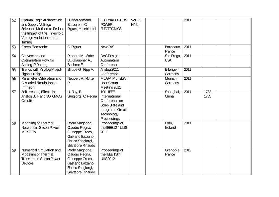
52 Optimal Logic Architecture and Supply Voltage Selection Method to Reduce the Impact of the Threshold Voltage Variation on the Timing
B. Kheradmand Boroujeni, C. Piguet, Y. Leblebici
JOURNAL OF LOW POWER ELECTRONICS
Vol. 7, N° 2,
2011
53 Green Electronics C. Piguet NewCAS Bordeaux, France
2011
54 Conversion and Optimization Flow for Analog IP Porting
Pronath M., Sobe U., Graupner A., Boehme E.
DAC Design Automation Conference
San Diego, USA
2011
55 Trends with Analog Mixed-Signal Design
Strube G., Ripp A. Analog 2011 Conference
Erlangen, Germany
2011
56 Parameter Calibration and Cascaded Simulations - Infineon
Neubert R., Rotter P.
MUGM MunEDA User Group Meeting 2011
Munich, Germany
2011
57 Self-Heating Effects in Analog Bulk and SOI CMOS Circuits
U. Roy, E. Sangiorgi, C. Fiegna
10th IEEE International Conference on Solid-State and Integrated Circuit Technology Proceedings
Shanghai, China
2011 1782 - 1785
58 Modeling of Thermal Network in Silicon Power MOSFETs
Paolo Magnone, Claudio Fiegna, Giuseppe Greco, Gaetano Bazzano, Enrico Sangiorgi, Salvatore Rinaudo
Proceedings of the IEEE 12th ULIS 2011
Cork, Ireland
2011
59 Numerical Simulation and Modeling of Thermal Transient in Silicon Power Devices
Paolo Magnone, Claudio Fiegna, Giuseppe Greco, Gaetano Bazzano, Enrico Sangiorgi, Salvatore Rinaudo
Proceedings of the IEEE 13th ULIS 2012
Grenoble, France
2012

60 Modeling, Control and Management of Thermal Effects in Electronic Circuits of the Future
Giuseppe Greco, Salvatore Rinaudo, Steffen Holland
European Nanoelectronics Forum
Munich, Germany
2012
61 Investigating the Effects of Inverted Temperature Dependence (ITD) on Clock Distribution Networks
Sassone A., Calimera A., Macii A., Macii E., Poncino M., Goldman R., Melikyan V., Babayan E., Rinaudo S.
Proceedings of Design, Automation & Test in Europe (DATE’12) conference
Dresden, Germany
2012 165-166
62 Thermal Via’s Placement Zones Identifying Using Voronoi Diagrams
Melikyan V., Gevorgyan A., Baghdasaryan A., Melikyan H.
Proceedings of the 32th International Scientific Conference Electronics and Nanotechnology (ELNANO 2012)
Kiev, Ukraine
2012 77-79
63 Method of Reducing Thermal Dependence of Timing Delays of Digital Integrated Circuits
Melikyan V., Babayan E., Harutyunyan A., Melikyan N., Zargaryan G.
Proceedings of 5th All-Russian scientific-technical conference “Problems of Developing Advanced Micro- and Nanoelectronic Systems -2012” (MES-2012)
Moscow, Russia
2012 409-412
64 Process-voltage -temperature Variation Detection and Cancellation Using On-Chip Phase-Locked
Melikyan V.Sh, Durgaryan A.A., Balabanyan A.H., Babayan E.H.,
Proceedings of the 56th Electronics, Telecommunicati
Zlatibor, Serbia
2012 EL1.2-1-4

Loop Stanojlovic M., Harutyunyan A.G.
ons, Computers, Automatic Control and Nuclear Engineering (ETRAN) Conference
65 A. Pattern-Based Approach to Current Density Verification
Melikyan V., Babayan E., Harutyunyan
Proceedings of the 4th Small Systems Simulation Symposium 2012
Nis, Serbia 2012 58-61
66 Decreasing of Frequency Variation in High-Speed Ring Oscillator using Bandgap Reference
Melikyan V., Balabanyan A., Babayan E., Durgaryan A.
Proceedings of the 32th International Scientific Conference Electronics and Nanotechnology (ELNANO 2012)
Kiev, Ukraine
2012 79-81
67 Synopsys’ Low Power Design Educational Platform
Roldman R., Bartleson K., Wood T., Melikyan V., Babayan E.
Proceedings of the 9th European Workshop on Microelectronics Education (EWME 2012)
Grenoble, France
2012 23-26
68 Pattern-Based Approach to Current Density Verification
Melikyan V., Babayan E., Harutyunyan A.
Electronics, Faculty of Electrical Engineering, University of Banja Luka, Volume 16, Number 1
Banja Luka, Serbia
2012 77-82
69 Modeling of IC Interconnects and Power
Melikyan V., Harutyunyan A.
Chartarapet Yerevan, Armenia
2012

Rails 70 Self-compensating Low
Noise Low Power PLL Design Melikyan V., Durgaryan A., Khachatryan A., Manukyan H., Musayelyan E.
Proceedings of IEEE East-West Design & Test Symposium (EWDTS’12)
Kharkov, Ukraine
2012 29-33
71 On-die CMOS Termination Resistor for USB Transmitter
Melikyan V. Sh., Gavrilov S.V., Aharonyan V.K., Aslanyan N.K., Hovhannisyan A.S.
RAs National Academy of Science and SEUA, Yerevan, RA
Vol. 65, N 3
Yerevan, Armenia
2012 295-304
72 Layout-Driven Post-Placement Techniques for Temperature Reduction and Thermal Gradient Minimization
Wei Liu; Calimera, A.; Nannarelli, A.; Macii, E.; Poncino M
IEEE Transactions on Computer-Aided Design of Integrated Circuits and Systems
2012
73 Modeling and characterization of thermally induced s kew on clock distribution networks of nanometric ICs
Sassone, A; Liu, Wei, Calimera A., Macii, A.; Macii, E; Poncino, M.
Elsevier Microelectronics Journal 2012
DOI: 10.1016/j.bbr.2011.03.031
2012
74 On the Efficacy of Layout Constrained Body-Biasing for Temperature Induced Clock-Skew Compensation
Tenace, V.; Miryala, S.; Calimera, A.; Macii, A.; Macii, E.; Poncino, M.
THERMINIC-12: IEEE International Workshop on Thermal Investigations of ICs and Systems
Budapest, Hungary
2012
75 Phase space based NBTI model
Reef Eilers, Malte Metzdorf, Sven Rosinger, Domenik Helms, Wolfgang Nebel
Proc. of International Workshop on Power and Timing Modeling, Optimization and Simulation
New Castle, UK
2012

(PATMOS), 2012 76 A quasi-SPICE electro-
thermal simulator Szalai Albin, Czirkos Zoltán, Székely Vladimír
Proceedings of the 18th International Workshop on THERMal INvestigation of ICs and Systems (THERMINIC'12)
Budapest, Hungary
2012 190-195
77 Yield enhancement by logi-thermal simulation based testing
Gergely Nagy, László Pohl, András Timár, András Poppe
Proceedings of the 18th International Workshop on THERMal INvestigation of ICs and Systems (THERMINIC'12)
Budapest, Hungary
2012 196-199
78 New simulation approaches supporting temperature-aware design of digital ICs
Gergely Nagy, András Timár, Albin Szalai, Márta Rencz, András Poppe
Proceedings of the 28th IEEE Semiconductor Thermal Measurement and Management Symposium (SEMI-THERM'12)
San Jose, CA, USA
313-318
79 Temperature dependent timing in standard cell designs
A Timar, M. Rencz Proceedings of the 18th International Workshop on THERMal INvestigation of ICs and Systems (THERMINIC'12)
Budapest, Hungary
2012 179-183
80 Real-time heating and power characterization of cells in standard cell designs
A Timar, M. Rencz MICROELECTRONICS JOURNAL
2012

81 Acquiring real-time heating of cells in standard cell designs
A Timar, M. Rencz Proceedings of the 13th IEEE Latin-American Test Workshop (LATW'12)
Quito, Ecuador
2012 121-125
82 Simulation Framework for Multilevel Power Estimation and Timing Analysis of Digital Systems Allowing the Consideration of Thermal Effects
Gergely Nagy, András Poppe
Proceedings of the 13th IEEE Latin-American Test Workshop (LATW'12)
Quito, Ecuador
2012 1-5
83 Maximum Delay Variation Temperature-Aware Standard Cell Design
Marc Pons, Jean-Luc Nagel and Christian Piguet
ICECS 2012 19th IEEE International Conference on Electronics, Circuits, and Systems
Seville, Spain
2012
84 Ultra-Low-Power Signal Processing in Autonomous Systems», Chapter 9 of Book « Energy Autonomous Micro and Nano Systems
C. Piguet Chapter 9 of Book “Energy Autonomous Micro and Nano Systems”
ISBN 978-1-84821-357-9
pp. 241-272
85 Process Variations Aware Design
M. Pons, F. Moll. C. Abella, C. Piguet
FETCH 2012 Alpes d’Huez, France
2012
86 Fixed Origin Corner Square Inspection Layout Regularity Metric
Marc Pons, Marc Morgan and Christian Piguet
DATE-12: IEEE Design Automation and Test in Europe
Dresden, German
2012
87 Coupled electro-thermal model for simulation of GaN power switching HEMTs in circuit simulators
Steve Stoffels, Herman Oprins, Denis Marcon, Karen Geens, Xuanwu Kang, Marleen Van Hove
Proceedings of the 18th International Workshop on THERMal INvestigation of
Budapest, Hungary
2012 1-6

and Stefaan Decoutere
ICs and Systems (THERMINIC'12)
88 Numerical and experimental characterization of hot spot dissipation in 3D stacks
Oprins H., Cherman V.
Electronics Cooling Magazine
Vol. 18(2)
2012 18-23
TEMPLATE A2: LIST OF DISSEMINATION ACTIVITIES
NO. Type of activities4 Main leader Title Date/Period Place Type of
audience5
Size of audience
Countries addressed
1 Conference POLITO DATE-10: IEEE Design Automation and Test in Europe
2010 Dresden, Germany
2 Conference POLITO GLSVLSI-10: ACM/IEEE Great Lakes Symposium on VLSI
2010 Providence, RI, USA
3 Conference POLITO ISCAS-10: IEEE International Conference on Circuits and Systems
2010 Paris, France
4 Conference POLITO DAC-10: ACM/IEEE Design Automation Conference
2010 Anaheim, CA, USA
4 A drop down list allows choosing the dissemination activity: publications, conferences, workshops, web, press releases, flyers, articles published in the popular press, videos, media briefings, presentations, exhibitions, thesis, interviews, films, TV clips, posters , Other.
5 A drop down list allows choosing the type of public: Scientific Community (higher education, Research), Industry, Civil Society, Policy makers, Medias, Other ('multiple choices' is possible).

5 Conference POLITO ISLPED-10: ACM/IEEE 2010 International Symposium on Low Power Electronics and Design
2010 Austin, TX, USA
6 Conference POLITO PATMOS-10: IEEE International Workshop on Power and Timing Modeling, Optimization and Simulation,
2010 Grenoble, France
7 Conference POLITO THERMINIC 2010: International Workshop on Thermal Investigation of ICs and Systems
2010
Barcelona, Spain
8 Conference POLITO ICCAD-10: IEEE/ACM International Conference on Computer-Aided Design
2010 San Jose, CA, USA
9 Course Macii E. ALARI Master Course 2010 Lugano, Switzerland
10 Course Macii E. First IEEE CASS Summer School, Physical Design of Reliable Circuits
2010 Porto Alegre, Brazil
11 Course Macii E. Microelectronics Summer School
2010 Florianopolis, Brazil
12 Conference Tutorial Calimera A., Macii A., Macii E., Poncino M.
ISCAS-10: IEEE International Conference on Circuits and Systems
2010 Paris, France

13 Conference Tutorial Atienza D., Ayala J.L., Calimera A.
ICECS 2010: IEEE International Conference on Electronics, Circuits, and Systems
2010 Athens, Greece
14 Course C. Piguet ENSEIRB 2011 Bordeaux, France
15 Conference SNPS-AM International conference “Moscow-Bavarian Joint Advanced Student School
2011 Zelenograd, Russia
16 Conference SNPS-AM 55th International Conference on Electronics, Telecommunications, Computers, Automatic Control and Nuclear Engineering (ETRAN’11),
2011 Banja Vrucica, Serbia
17 Conference SNPS-AM 8th International Conference of “Semiconductor Micro- and Nanoelectronics
2011 Yerevan, Armenia
18 Conference SNPS-AM ASIA Power Architecture Conference
2011 Shenzhen, China
19 Conference SNPS-AM 9th IEEE East-West Design & Test Symposium (EWDTS’11)
2011 Sevastopol, Ukraine
20 Conference SNPS-AM International conference
2011 Yerevan, Armenia

“Education, Science and Economics at Universities. Integration to International Educational Area”
21 Conference SNPS-AM 6th IEEE International Design and Test Workshop (IDT) in Conjunction with IEEE International Conference on Electronics, Circuits and Systems (ICECS)
2011 Beirut, Lebanon
22 Tutorial Chan-Su Yun, Tommaso Cilento, Guenther Zandler
Therminator tutorial 2011 Munich, Germany
23 Tutorial Vazgen Melikyan
8th International Conference of “Semiconductor Micro- and Nanoelectronics
2011 Yerevan, Armenia
24 Tutorial Vazgen Melikyan
Moscow-Bavarian Joint School Conference
2011 Zelenograd, Russia
25 Tutorial Shushan Karapetyan
Moscow-Bavarian Joint School Conference
2011 Zelenograd, Russia
26 Tutorial Shushan Karapetyan, Vazgen Melikyan
Moscow-Bavarian Joint School Conference
2011 Zelenograd, Russia

27 Conference POLITO DATE-11: IEEE Design Automation and Test in Europe
2011 Grenoble, France
28 Conference POLITO GLSVLSI-11: ACM/IEEE Great Lakes Symposium on VLSI
2011 Lausanne, Switzerland
29 Conference POLITO ISCAS-11: IEEE International Conference on Circuits and Systems
2011 Rio de Janeiro, Brazil
30 Conference POLITO DAC-11: ACM/IEEE Design Automation Conference
2011 San Diego, CA, USA
31 Conference POLITO ISLPED-11: ACM/IEEE 2010 International Symposium on Low Power Electronics and Design
2011 Fukuoka, Japan
32 Conference POLITO PATMOS-11: IEEE International Workshop on Power and Timing Modeling, Optimization and Simulation
2011 Madrid, Spain
33 Conference POLITO THERMINIC 2011: International Workshop on Thermal Investigation of ICs and Systems
2011 Paris, France,
34 Conference POLITO ICCAD-11: IEEE/ACM International Conference on
2011 San Jose, CA, USA

Computer-Aided Design
35 Keynote speech Enrico Macii IEEE Prime Asia 2011 2011 Macau, China
36 Course Enrico Macii ALARI Master Course 2011 Lugano, Switzerland
37 Course Andrea Calimera, Alberto Macii
Therminator Course (Basic)
2011 Torino, Italy
38 Course Andrea Calimera, Alberto Macii
Therminator Course (Advanced)
2011 Torino, Italy
39 Conference IMEC SEMI-Therm-11: 27th Annual IEEE Thermal Measurement, Modeling and Management Symposium
2011 San Jose, CA, USA
40 Conference IMEC THERMINIC 2011: International Workshop on Thermal Investigation of ICs and Systems
2011 Paris, France
41 Conference FHG THERMINIC 2011: International Workshop on Thermal Investigation of ICs and Systems
2011 Paris, France
42 Tutorial A. Burenkov Therminator Tutorial at Intel Mobile
2011 Munich, Germany

Communication 43 Workshop NXP, FHG,
MunEDA THERMINATOR MunEDA - Workshop and Training
2011 Hamburg, Germany
44 Course Sven Rosinger, Malte Metzdorf, Patrick Knocke
IEEE Xplore - Educational Courses
2011 WEB
45 Tutorial Joachim Assenmacher
Therminator tutorial 2011 Munich, Germany
46 Tutorial Christian Pach, Klaus von Arnim
Therminator tutorial 2011 Munich, Germany
47 Course C. Piguet EPFL Course 2011 Lausanne, Switzerland
48 Course C. Piguet ALaRI Course 2011 Lugano, Switzerland
49 Workshop MUNEDA THERMINATOR Joined Contribution Synopsys-MunEDA at MTF Korea 2011
2011 Seoul, Korea
50 Workshop MUNEDA THERMINATOR MunEDA –Workshop and Training
2011 Catania, Italy
51 Workshop MUNEDA THERMINATOR MunEDA –Workshop and Training
2011 Crolles, France
52 Workshop MUNEDA THERMINATOR MunEDA –Workshop and Training
2011 Castelletto, Italy
53 Workshop MUNEDA THERMINATOR MunEDA –Workshop and Training
2011 Villacon, Germany

54 Workshop MUNEDA THERMINATOR MunEDA –Workshop and Training
2011 Hamburg, Germany
55 Conference UNIBO 10th IEEE International Conference on Solid-State and Integrated Circuit Technology
2011 Shanghai, China
56 Conference UNIBO Ultimate Integration on Silicon Conference
2011 Cork, Ireland
57 Course R. Guerrieri University of Bologna course
2011 Bologna, Italy
58 Course R. Guerrieri University of Bologna course
2011 Bologna, Italy
59 Seminar Cilento T. MRS SPRING MEETING
2012
60 Course SNPS-AM Master Course in State Engineering University of Armenia Advanced IC Physical Design
2012 Yerevan, Armenia
61 Course SNPS-AM Master Course in Moscow Institute of Electronic Technology
2012 Moscow, Russia
62 Course SNPS-AM Master Course in Moscow-Bavarian Joint Advanced Student School
2012 Moscow, Russia
63 Conference POLITO DATE-12: IEEE Design Automation and Test in Europe
2012 Dresden, Germany
64 Conference POLITO GLSVLSI-12: ACM/IEEE Great
2012 Salt Lake City, USA

Lakes Symposium on VLSI
65 Conference POLITO ISCAS-12: IEEE International Conference on Circuits and Systems
2012 Seoul, Korea
66 Conference POLITO DAC-12: ACM/IEEE Design Automation Conference
2012 San Francisco, CA, USA
67 Conference POLITO ISLPED-12: ACM/IEEE 2010 International Symposium on Low Power Electronics and Design
2012 Redondo Beach, CA, USA
68 Conference POLITO PATMOS-12: IEEE International Workshop on Power and Timing Modeling, Optimization and Simulation,
2012 New Castle, UK
69 Conference POLITO THERMINIC 2012: International Workshop on Thermal Investigation of ICs and Systems
2012
Budapest, Hungary
70 Conference POLITO ICCAD-12: IEEE/ACM International Conference on Computer-Aided Design
2012 San Jose, Ca, USA
71 Course Macii E. ALARI Master Course 2012 Lugano, Switzerland
72 Seminar Macii E. Seminar at 2012 San

University of California Berkeley
Francisco, CA, USA
73 Seminar Macii E. Seminar at University of California Los Angeles (UCLA)
2012 Los Angeles, CA, USA
74 Seminar Macii E. Seminar at the SEOUL NATIONAL UNIVERSITY
2012 Seoul, Korea
75 Invited speech Macii E. Invited speech at STMicroelectronics, Catania
2012 Catania, Italy
76 Seminar Macii E. Seminar at the École Polytechnique Fédérale de Lausanne (EPFL)
2012 Lausanne, Switzerland
77 Course Andrea Calimera, Alberto Macii
Therminator Course (Basic)
2012 Torino, Italy
78 Course Andrea Calimera, Alberto Macii
Therminator Course (Advanced)
2012 Torino, Italy
79 Course Sven Rosinger, Patrick Knocke
Lectures at OFFIS 2012 Oldenburg, Germany
80 Conference Márta Rencz LATW 2012 (Quito, Ecuador) – Special session 3: Thermal Aware Design and Test (Friday, April 13th 2012)
2012 Quito, Ecuador
81 Conference András Therminic 2012 2012 Budapest,

Poppe (Budapest, Hungary) – Therminator session (Wednesday, September 26th 2012)
Hungary
82 Keynote Speech C. Piguet IEEE Faible Tension Faible Consommation (FTFC) 2012
2012 Paris, France
83 Conference CSEM ICECS 2012: IEEE International Conference on Electronics, Circuits, and Systems
2012 Seville, Spain
84 Conference CSEM DATE-12: IEEE Design Automation and Test in Europe
2012 Dresden, Germany
85 Conference CSEM FETCH 2012: Ecole d'hiver Francophone sur les Technologies de Conception des Systèmes embarqués Hétérogènes
2012 Alpe d'Huez, France
86 Conference CSEM FTFC 2012: IEEE Faible Tension Faible Consommation
2012 Paris, France
87 Course C. Piguet ALaRI Course on Embedded Systems, University of Lugano
2012 Lugano, Switzerland
88 Course C. Piguet Course at EPFL, Lausanne
2012 Lausanne, Switzerland
89 Course C. Piguet Course at ISEP, Paris 2012 (Apr.) Paris, France 90 Course C. Piguet Course at ISEP, Paris 2012 (Sept.) Paris, France

Section B (Confidential6 or public: confidential information to be marked clearly) Part B1 At the moment there is no ahe applications for patents, trademarks, registered designs, etc
Part B2 Please complete the table hereafter:
Exploitable Knowledge (description under the ref. below)
Exploitable product(s) or measure(s)
Sector(s) of application
Patents or other
IPR protection
Owner & Other
Partner(s) involved
WP
THERMINATOR-IP1 Flow for temperature estimation and optimization of designs specified at behavioral-level
Thermal estimation and optimisation
OFFIS 6
THERMINATOR IP2 PAN extention to the thermal frame
Thermal optimisation ST 5
THERMINATOR-IP3 training BME 8
THERMINATOR-IP4 Logithermal simulator EDA tool BME, POLITO, UNIBO
3
THERMINATOR-IP5 Model for distributed thermal effect in Si wafer
EDA UniBO 5
THERMINATOR-IP6 MPSoC chip Chip Design LETI, CSEM 3
THERMINATOR-IP7 Temperature sensor Chip Design, temperature control
LETI 3
THERMINATOR-IP8 Local controllers for dynamic thermal and power management, running a game theory-based algorithm
Chip Design, Methodology
LETI 3
6 Note to be confused with the "EU CONFIDENTIAL" classification for some security research projects.

Relevant details of exploitable result
A short scheme is provided on an individual IP basis.
THERMINATOR - IP 1: Behavioral-level thermal and aging estimation flow ? Owner/proposer
OFFIS
? Result A thermal and aging estimation flow starting with a behavioural-level design description in C/SystemC has been developed. The design is power-estimated and, together with an IC package description, it is iterated through different tools in order to include electro-thermal coupling as well as voltage drops in the supply grid. A second iteration loop considers the long term degradation aspects due to the NBTI effect. The flow integrates existing and new methodologies/tools from the energy-, thermal- and reliability-estimation domains and links them to work together.
? Partner(s) involved OFFIS, ChipVision (from M1 to M12).
? How the result might be exploited The developed flow is published in scientific papers. Prototype tools have been developed to evaluate the flow. Third party tool vendors may provide integration into EDA tools. Further additional research and development work. Within new research projects, the simulation framework developed in THERMINATOR will be maintained for new technologies such as FinFETs and more complex IC packages. For instance 3D designs with stacked die layers and appropriate interconnect layers will require significant but nonetheless feasible modifications. Especially through-silicon-vias having the intent to spread the heat demand for a further extension of the simulation capabilities. On the other hand, the estimation flow will be extended to additional process metrics related to parameter degradation. Up to now only models for the NBTI effects are available but other effects will also impact the degradation. Example: the knowledge of the temperature distribution and power density distribution – both already available in the THERMINATOR flow – is sufficient for an electro-migration prediction. Another major item for the model exploitation is to raise the input level of the entire estimation framework. The ultimate goal here is the development of a system-level multi-physics design flow for heterogeneous 3D SiP designs leading to a market-ready product.
? Intellectual Property Rights protection measures additional research and development work None
? Any commercial contacts already taken, demonstrations given to potential licensees and/or investors and any comments received None
? Any other potential impact from the exploitation of the result None

THERMINATOR - IP2: PAN extension to the thermal frame ? Owner/Assignee ST ? Result:
Functional Prototype by M36
? Partner(s) involved OFFIS
? How the result might be exploited Third party EDA, new simulation tool
? Further additional research and development work New methodology regarding reliability and degradation will have to be integrated into the simulation framework.
? Intellectual Property Rights protection measures additional research and development work THERMINATOR IPCA
? Any commercial contacts already taken, demonstrations given to potential licensees and/or investors and any comments received
? Some discussion occurred between ST and Synopsys top management, it is quite confidential.
? Any other potential impact from the exploitation of the result With the simulation methodology
THERMINATOR - IP3: Training ? Owner/proposer
BME
? Result
The R&D partners of the project have worked together on the p reparation of the material for a comprehensive set of training modules, covering basic and advanced aspects of thermal aware design methods in nanometric designs. The course material has been made available by month M12 of the project, and was updated at month M24, according to the research results achieved along the project.
During the whole project duration, THERMINATOR has organized and executed Courses and Workshops across Europe.
Duration of the courses ranges from 7h (i.e. one day) to 14h (i.e. two d ays). Theoretical lectures, training material and demo sessions are available (restricted to programme participants). Instructors for the courses have been selected by the involved partners within their own organizations.
Materials:
? Modelling and characterization of thermal effects in discrete semiconductor devices

? Introduction to electro-thermal simulation ? High-level thermal estimation ? Synopsys design flow tutorial ? MunEDA design flow tutorial
Events:
? Workshop at the headquarters of IMC, Munich A workshop with the participation of several Therminator partners was proposed by IMC. The following partners are invited to the tutorial/workshop: FHG Erlangen, Synopsys, Uni Hamburg, NXP, FHG Dresden, and IMC. The tutorial will present material for a comprehensive set of training modules, covering basic and advanced aspects of the key topics worked out in the different Therminator work packages. A duration of 6 hours is planned. Three basic and three advanced presentations, each of one hour duration, have been planned. The topics are the following:
Partner Topic
FHG Erlangen TCAD simulations of Nano-CMOS incl. Self-heating
Synopsys, Switzerland TCAD: CMOS degradation mechanisms (NBTI, HCI…),
FinFET modelling and calibration, incl. temperature effects
Uni Hamburg, NXP digital temperature sensor
FHG Dresden Simulation of electro-thermal interaction effects in electronic circuits
IMC Comparison of compact modelling strategies between BSIM and PSP incl. Temperature modelling
? Workshop at Therminic 2011, Paris Two special Therminator Sessions will be held at the Therminic 2011 conference in Paris. The proposed topics are the following:
Partner Topic
Marta Rencz (BME) THE THERMINATOR PROJECT: MIDWAY ACHIEVEMENTS AND

PERSPECTIVES
Giuseppe Greco, Gaetano Bazzano, Daniela Grazia, Cavallaro, (STMicroelectronics, Italy)
AN ANALOG BEHAVIORAL THERMAL MACRO-MODEL AIMED AT
REPRESENTING AN ELEMENTARY PORTION OF A DISCRETE IGBT
POWER DEVICE
Alex Burenkov, Jurgen Lorenz (Fraunhofer Institute for Integrated Systems and
Device Technology, Germany)
SELF-HEATING EFFECTS IN NANO-SCALED MOSFETS AND
THERMAL AWARE COMPACT MODELS
Jean-Christophe Krencker, Luc Hébrard, Jean-Baptiste Kammerer, Yannick
Hervé (InESS, Strasbourg, France)
3D ELECTRO-THERMAL SIMULATIONS OF ANALOG ICS CARRIED
OUT WITH STANDARD CAD TOOLS AND VERILOG-A
Alessandro Sassone, Wei Liu, Andrea Calimera, Alberto Macii, Enrico Macii,
Massimo Poncino (Politecnico di Torino, Italy)
ON THE MODELING OF THERMALLY INDUCED SKEW IN CLOCK
DISTRIBUTION NETWORK
András Timár, György Bognár, Marta Rencz (BME)
IMPROVED POWER MODELING IN LOGI-THERMAL SIMULATION
Gergely Nagy, András Poppe (BME)
A NOVEL SIMULATION ENVIRONMENT ENABLING MULTILEVEL
POWER ESTIMATION OF DIGITAL SYSTEMS
Sven Reitz, Andy Heinig, Roland Martin, Jörn Stolle, Andreas Wilde (Fraunhofer Institute for
Integrated Circuits,
THERMAL MODELING OF 3D STACKS FOR FLOORPLANNING

Germany)
Steve Stoffels, Denis Marcon, Karen Geens, Xuanwu Kang, Geert Van Der Plas,
Marleen Van Hove, Stefaan Decoutere (IMEC, Belgium)
HIGH TEMPERATURE CALIBRATION OF A COMPACT MODEL FOR
GAN-ON-SI POWER SWITCHES
Mohammadsadegh Sadri, Andrea Bartolini, Luca Benini (University of Bologna,
Italy)
SINGLE-CHIP CLOUD COMPUTER THERMAL MODEL
? Webinar made by Synopsys Switzerland Synopsys plans two training courses of half a day or one day each at the Zurich office. The courses are planned as follows:
Topic: Electro-thermal 2D and 3D TCAD simulation
Level: Introductory
Abstract: The presentation shows how to use TCAD tools for the simulation of electro-thermal problems in semiconductor devices. The lecture starts from the generation and meshing of the 2D or 3D structure, introduces and discusses the device models, and ends with the discussion of simulation results.
Topic: Temperature effects in device models - separation and extraction of temperature effects
Level: Advanced
Abstract: The presentation discusses the state of the art device simulation models with respect to their temperature dependence. Ways to calibrate model parameters and to extract temperature dependence of compact model

parameters from device simulation are treated.
Schedule: planned for M30-36.
? Partner(s) involved All partners in the project.
? How the result might be exploited On-site execution of the Course upon request. Diffusion of the presentations through EuroTraining.
? Further additional research and development work Course updating according to work plan.
? Intellectual Property Rights protection measures None.
? Any commercial contacts already taken, demonstrations given to potential licensees and/or investors and any comments received None.
? Any other potential impact from the exploitation of the result None.
THERMINATOR - IP4: Logithermal Simulator ? Owner/proposer
BME
? Result The partners have developed a new simulation method that models the thermal behaviour of logic circuits accounting for their self heating, due to dissipation and timing changes, subsequent to the temperature dependency of gate delays.
? Partner(s) involved POLITO, UNIBO
? How the result might be exploited This new tool can play an important role in researches aiming at investigating and developing new, thermal aware design methods for digital systems. It may also become an integral part of CAD tools as it can provide a very important input to place-and-route algorithms, to find possible hot spots and areas where strict timing conditions might be broken because of thermal effects. Thus a major industrial exploitation of this result can be anticipated in the near future.

? Further additional research and development work Place-and-route algorithms based on the results yielded by logithermal simulations should be developed.
? Intellectual Property Rights protection measures None.
? Any commercial contacts already taken, demonstrations given to potential licensees and/or investors and any comments received None.
? Any other potential impact from the exploitation of the result None.
THERMINATOR - IP5: Model for distributed thermal effect in Si wafer ? Owner/proposer
UNIBO
? Result A model based on equivalent electrical RC network for the modelling of distributed time-dependent 2-D thermal effects in the silicon substrate has been developed and validated versus numerical simulations
? Partner(s) involved UNIBO, STM.
? How the result might be exploited Transfer to STM for implementation in EDA tools, evaluate involvement of EDA SW House.
? Further additional research and development work Extension to 3D and comparison with experimental data
? Intellectual Property Rights protection measures None
? Any commercial contacts already taken, demonstrations given to potential licensees and/or investors and any comments received None.
? Any other potential impact from the exploitation of the result Application to the optimization of discrete power devices
THERMINATOR - IP6: MPSoC Chip ? Owner/Assignee LETI, CSEM ? Result:

An Integrated circuit called GENEPY comprising 6 clusters (or SMEP), each cluster having one controller and two DSP processors. Communication between the clusters has been implemented through an asynchronous NoC.
? Partner(s) involved
LETI, CSEM
? How the result might be exploited The GENEPY Chip can be re-used by other EU projects (it will be the case in EU project TouchMore) or other research projects. The chip can be re-used for industrial projects under a license.
? Further additional research and development work Development tools for the GENEPY chip have to be improved.
? Intellectual Property Rights protection measures Patent submission ID:
LETI: The NoC used in Genepy is protected by patents no. EP1641197, EP1701273, EP1701274.CSEM: no icyflex patent
? Any commercial contacts already taken, demonstrations given to potential licensees and/or investors and any comments received Not yet for the GENEPY platform, but many CSEM industrial projects based on the icyflex2 controller and icyflex4 DSP.
? Any other potential impact from the exploitation of the result None
THERMINATOR - IP 7: Temperature sensor ? Owner/Assignee LETI ? Result: A fine-granularity, scalable, full-CMOS temperature sensor based on ring oscillators’ frequency comparison. Its small size, combined with its standard cell-based design, enables it to be inserted into virtually any functional unit thus providing fine-grain temperature monitoring.
? Partner(s) involved
None
? How the result might be exploited This temperature sensor can be reused into any chip design requiring temperature to be monitored, without requiring any additional process step (contrary to bipolar-based temperature sensors).
? Further additional research and development work

This special design, made especially sensitive to temperature variations, can be further refined to render it sensitive to supply voltage or technological parameters like threshold voltage, making it a suitable PVT sensor.
? Intellectual Property Rights protection measures None
? Any commercial contacts already taken, demonstrations given to potential licensees and/or investors and any comments received This sensor has been inserted into a test chip done with STMicroelectronics, in a more advanced technological node, which needed a complete redesign of the sensor.
? Any other potential impact from the exploitation of the result None
THERMINATOR - IP 8: Local controllers for dynamic thermal and power management ? Owner/Assignee LETI ? Result: Local controllers to optimize the couple (supply voltage/clock frequency) in order to perform dynamic thermal and power management, while taking into account applications’ specific constraints, e.g. required task completion time. Those controllers look for a consensus by running a distributed algorithm based on game theory.
? Partner(s) involved
None
? How the result might be exploited Those local controllers, and the associated methodology, can be reused into any MPSOC (Multi-Processor System-On-Chip) platform whose thermal and/or power dissipation constraints necessitate to finely tune operating parameters.
? Further additional research and development work None
? Intellectual Property Rights protection measures None
? Any commercial contacts already taken, demonstrations given to potential licensees and/or investors and any comments received None
? Any other potential impact from the exploitation of the result None

1.3 Report on societal implications
A General Information (completed automatically when Grant Agreement number is entered.
Grant Agreement Number: 248603
Title of Project: Modelling, Control and Management of Thermal Effects in
Electronic Circuits of the Future
Name and Title of Coordinator: Ing Salvatore Rinaudo, Director, IMS CAD Design Services
B Ethics
1. Did your project undergo an Ethics Review (and/or Screening)?
? If Yes: have you described the progress of compliance with the relevant Ethics
Review/Screening Requirements in the frame of the periodic/final project reports? Special Reminder: the progress of compliance with the Ethics Review/Screening Requirements should be described in the Period/Final Project Reports under the Section 3.2.2 'Work Progress and Achievements'
YES
Yes
2. Please indicate whether your project involved any of the following issues (tick box) :
YES
RESEARCH ON HUMANS ? Did the project involve children? No ? Did the project involve patients? No ? Did the project involve persons not able to give consent? No ? Did the project involve adult healthy volunteers? No ? Did the project involve Human genetic material? No ? Did the project involve Human biological samples? No ? Did the project involve Human data collection? No
RESEARCH ON HUMAN EMBRYO/FOETUS ? Did the project involve Human Embryos? No ? Did the project involve Human Foetal Tissue / Cells? No ? Did the project involve Human Embryonic Stem Cells (hESCs)? No ? Did the project on human Embryonic Stem Cells involve cells in culture? No ? Did the project on human Embryonic Stem Cells involve the derivation of cells from Embryos? No
PRIVACYNO ? Did the project involve processing of genetic information or personal data (eg. health, sexual
lifestyle, ethnicity, political opinion, religious or philosophical conviction)? NO
? Did the project involve tracking the location or observation of people? NO RESEARCH ON ANIMALS
? Did the project involve research on animals? No ? Were those animals transgenic small laboratory animals? No ? Were those animals transgenic farm animals? No ? Were those animals cloned farm animals? No ? Were those animals non-human primates? No
RESEARCH INVOLVING DEVELOPING COUNTRIES ? Did the project involve the use of local resources (genetic, animal, plant etc)? No

? Was the project of benefit to local community (capacity building, access to healthcare, education etc)?
No
DUAL USE ? Research having direct military use No
? Research having the potential for terrorist abuse No
C Workforce Statistics
3. Workforce statistics for the project: Please indicate in the table below the number of people who worked on the project (on a headcount basis).
Type of Position Number of Women Number of Men
Scientific Coordinator 0 23
Work package leaders 2 13 Experienced researchers (i.e. PhD holders) 4 73 PhD Students 0 8 Other 9 15
4. How many additional researchers (in companies and universities) were recruited specifically for this project?
7
Of which, indicate the number of men:
7

D Gender Aspects 5. Did you carry out specific Gender Equality Actions under the project?
? ?
Yes No
6. Which of the following actions did you carry out and how effective were they? Not at all
effective Very
effective
? Design and implement an equal opportunity policy ? ? ? ? ? ? Set targets to achieve a gender balance in the workforce ? ? ? ? ? ? Organise conferences and workshops on gender ? ? ? ? ? ? Actions to improve work-life balance ? ? ? ? ? ? Other:
7. Was there a gender dimension associated with the research content – i.e. wherever people were the focus of the research as, for example, consumers, users, patients or in trials, was the issue of gender considered and addressed?
? Yes- please specify
? No
E Synergies with Science Education
8. Did your project involve working with students and/or school pupils (e.g. open days, participation in science festivals and events, prizes/competitions or joint projects)?
? Yes- please specify
? No
9. Did the project generate any science education material (e.g. kits, websites, explanatory booklets, DVDs)?
? Yes- please specify
? No
F Interdisciplinarity
10. Which disciplines (see list below) are involved in your project? ? Main discipline7: 2.2 ? Associated discipline7:1.2 ? Associated discipline7:1.1
G Engaging with Civil society and policy makers
11a Did your project engage with societal actors beyond the research community? (if 'No', go to Question 14)
? ?
Yes No
11b If yes, did you engage with citizens (citizens' panels / juries) or organised civil society (NGOs, patients' groups etc.)?
? No ? Yes- in determining what research should be performed ? Yes - in implementing the research ? Yes, in communicating /disseminating / using the results of the project
7 Insert number from list below (Frascati Manual).

11c In doing so, did your project involve actors whose role is mainly to organise the dialogue with citizens and organised civil society (e.g. professional mediator; communication company, science museums)?
? ?
Yes No
12. Did you engage with government / public bodies or policy makers (including international organisations)
? No ? Yes- in framing the research agenda ? Yes - in implementing the research agenda ? Yes, in communicating /disseminating / using t he results of the project
13a Will the project generate outputs (expertise or scientific advice) which could be used by policy makers?
? Yes – as a primary objective (please indicate areas below- multiple answers possible) ? Yes – as a secondary objective (please indicate areas below - multiple answer possible) ? No
13b If Yes, in which fields? Agriculture Audiovisual and Media Budget Competition Consumers Culture Customs Development Economic and Monetary Affairs Education, Training, Youth Employment and Social Affairs
Energy Enlargement Enterprise Environment External Relations External Trade Fisheries and Maritime Affairs Food Safety Foreign and Security Policy Fraud Humanitarian aid
Human rights Information Society Institutional affairs Internal Market Justice, freedom and security Public Health Regional Policy Research and Innovation Space Taxation Transport

13c If Yes, at which level? ? Local / regional levels ? National level ? European level ? International level
H Use and dissemination
14. How many Articles were published/accepted for publication in peer-reviewed journals?
88
To how many of these is open access8 provided? 88
How many of these are published in open access journals? 17
How many of these are published in open repositories? 88
To how many of these is open access not provided? 0
Please check all applicable reasons for not providing open access:
? publisher's licensing agreement would not permit publishing in a repository ? no suitable repository available ? no suitable open access journal available ? no funds available to publish in an open access journal ? lack of time and resources ? lack of information on open access ? other9: ……………
15. How many new patent applications (‘priority filings’) have been made? ("Technologically unique": multiple applications for the same invention in different jurisdictions should be counted as just one application of g rant).
0
16. Indicate how many of the following Intellectual Property Rights were applied for (give number in each box).
Trademark 0
Registered design 0
Other 0
17. How many spin-off companies were created / are planned as a direct result of the project?
0
Indicate the approximate number of additional jobs in these companies:
18. Please indicate whether your project has a potential impact on employment, in comparison with the situation before your project:
? Increase in employment, or ? In small & medium-sized enterprises ? Safeguard employment, or ? In large companies ? Decrease in employment, ? None of the above / not relevant to the project ? Difficult to estimate / not possible to quantify
19. For your project partnership please estimate the employment effect resulting directly from your participation in Full Time Equivalent (FTE = one person working fulltime for a year) jobs:
Indicate figure: 30
8 Open Access is defined as free of charge access for anyone via Internet. 9 For instance: classification for security project.

Difficult to estimate / not possible to quantify
?
I Media and Communication to the general public
20. As part of the project, were any of the beneficiaries professionals in communication or media relations?
? Yes ? No
21. As part of the project, have any beneficiaries received professional media / communication training / advice to improve communication with the general public?
? Yes ? No
22 Which of the following have been used to communicate information about your project to the general public, or have resulted from your project?
? Press Release ? Coverage in specialist press ? Media briefing ? Coverage in general (non-specialist) press ? TV coverage / report ? Coverage in national press ? Radio coverage / report ? Coverage in international press ? Brochures /posters / flyers ? Website for the general public / internet ? DVD /Film /Multimedia ? Event targeting general public (festival, conference,
exhibition, science café)
23 In which languages are the information products for the general public produced?
? Language of the coordinator ? English ? Other language(s)
Question F-10: Classification of Scientific Disciplines according to the Frascati Manual 2002 (Proposed Standard Practice for Surveys on Research and Experimental Development, OECD 2002): FIELDS OF SCIENCE AND TECHNOLOGY 1. NATURAL SCIENCES 1.1 Mathematics and computer sciences [mathematics and other allied fields: computer sciences and other allied
subjects (software development only; hardware development should be classified in the engineering fields)] 1.2 Physical sciences (astronomy and space sciences, physics and other allied subjects) 1.3 Chemical sciences (chemistry, other allied subjects) 1.4 Earth and related environmental sciences (geology, geophysics, mineralogy, physical geography and other
geosciences, meteorology and other atmospheric sciences including climatic research, oceanography, vulcanology, palaeoecology, other allied sciences)
1.5 Biological sciences (biology, botany, bacteriology, microbiology, zoology, entomology, genetics, biochemistry, biophysics, other allied sciences, excluding clinical and veterinary sciences)
2 ENGINEERING AND TECHNOLOGY 2.1 Civil engineering (architecture engineering, building science and engineering, construction engineering,
municipal and structural engineering and other allied subjects) 2.2 Electrical engineering, electronics [electrical engineering, electronics, communication engineering and systems,
computer engineering (hardware only) and other allied subjects] 2.3. Other engineering sciences (such as chemical, aeronautical and space, mechanical, metallurgical and materials
engineering, and their specialised subdivisions; forest products; applied sciences such as geodesy, industrial

chemistry, etc.; the science and technology of food production; specialised technologies of interdisciplinary fields, e.g. systems analysis, metallurgy, mining, textile technology and other applied subjects)
3. MEDICAL SCIENCES 3.1 Basic medicine (anatomy, cytology, physiology, genetics, pharmacy, pharmacology, toxicology, immunology
and immunohaematology, clinical chemistry, clinical microbiology, pathology) 3.2 Clinical medicine (anaesthesiology, paediatrics, obstetrics and gynaecology, internal medicine, surgery,
dentistry, neurology, psychiatry, radiology, therapeutics, otorhinolaryngology, ophthalmology) 3.3 Health sciences (public health services, social medicine, hygiene, nursing, epidemiology) 4. AGRICULTURAL SCIENCES 4.1 Agriculture, forestry, fisheries and allied sciences (agronomy, animal husbandry, fisheries, forestry, horticulture,
other allied subjects) 4.2 Veterinary medicine 5. SOCIAL SCIENCES 5.1 Psychology 5.2 Economics 5.3 Educational sciences (education and training and other allied subjects) 5.4 Other social sciences [anthropology (social and cultural) and ethnology, demography, geography (human,
economic and social), town and country planning, management, law, linguistics, political sciences, sociology, organisation and methods, miscellaneous social sciences and interdisciplinary , methodological and his torical S1T activities relating to subjects in this group. Physical anthropology, physical geography and psychophysiology should normally be classified with the natural sciences].
6. HUMANITIES 6.1 History (history, prehistory and history, together with auxiliary historical disciplines such as archaeology,
numismatics, palaeography, genealogy, etc.) 6.2 Languages and literature (ancient and modern) 6.3 Other humanities [philosophy (including the history of science and technology) arts, history of art, art criticism,
painting, sculpture, musicology, dramatic art excluding artistic "research" of any kind, religion, theology, other fields and subjects pertaining to the humanities, methodological, historical and other S1T activities relating to the subjects in this group]


![ICT-2009.3.2 -IP Modelling, Control and Management of ... › docs › projects › cnect › 3 › 248603 › 080 › d… · (MOSRA) [1] adds ageing effects to industry-standard](https://img.dokumen.tips/doc/110x75/5f0e0f5f7e708231d43d6b3c/ict-200932-ip-modelling-control-and-management-of-a-docs-a-projects.jpg)