Embed Size (px)
Citation preview

Professional Education Seminar S17
Practical Application of 600 V GaN HEMTs in Power Electronics
Monday March 16, 2015 8:30 – 12:00
Eric Persson, GaN Applications
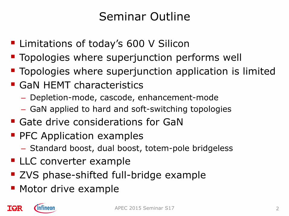
Seminar Outline
Limitations of today‟s 600 V Silicon
Topologies where superjunction performs well
Topologies where superjunction application is limited
GaN HEMT characteristics
– Depletion-mode, cascode, enhancement-mode
– GaN applied to hard and soft-switching topologies
Gate drive considerations for GaN
PFC Application examples
– Standard boost, dual boost, totem-pole bridgeless
LLC converter example
ZVS phase-shifted full-bridge example
Motor drive example
APEC 2015 Seminar S17 2

What needs improvement?
For same Rds(on), improve all the charge parameters:
Reduce Coss nonlinearity
– Nonlinearity makes timing and dv/dt control challenging
Reduce Qoss (and therefore Eoss) magnitude
Reduce Coss dissipation factor
Improve body diode dynamic performance
– Reduce/eliminate Qrr
Reduce gate charge
All of the above at affordable cost
APEC 2015 Seminar S17 3

Topologies where superjunction works well
Unipolar current flow, hard or soft-switched
Two-transistor forward
– Hard switched, partial valley switched
Boost PFC
– CCM or CrCM
Flyback
– Hard switched, partial valley switched
Why?
– Superjunction has low Rds(on)*Eoss figure of merit
– Body diode performance is not important
APEC 2015 Seminar S17 4

2-Transistor Forward Converter (2TF)
APEC 2015 Seminar S17 5
Vin

2TF voltage and current waveforms
APEC 2015 Seminar S17 6
Ref: Thierry Sutto, “2 switch forward current mode converter,” ON semi app note AND8373/D

2TF FET turn-on loss measurement
APEC 2015 Seminar S17 7
Ref: Thierry Sutto, “2 switch forward current mode converter,” ON semi app note AND8373/D

2TF FET turn-on loss analysis
This accounts for the “crossover” loss
– Where the transistor is supporting simultaneous V and I
What is missing?
This suggests that if Δt goes to 0, Turn-on loss = 0
APEC 2015 Seminar S17 8
Ref: Thierry Sutto, “2 switch forward current mode converter,” ON semi app note AND8373/D

What about the Eoss of the FET itself?
APEC 2015 Seminar S17 9
FD OI
1gdC
gsC
dV
GR
GGV
Equivalent Circuit
Simplified Schematic
dsC
akC
dV
oI
DSv
Di
Gi
SiC Schottky
t0
tiD
tvDS
dV
tPLOSS
Current Commutation Qsw Discharge
Note: This is not Qrr

2TF FET turn-off loss
Turn-off losses limited entirely by gate drive
– If you can turn-off the gate extremely fast, get ZVS
APEC 2015 Seminar S17 10
Ref: Thierry Sutto, “2 switch forward current mode converter,” ON semi app note AND8373/D

2 Transistor Forward Summary
This is a unipolar topology
– Superjunction already works well
– Body diode performance is unimportant
Switch losses are dominated by:
– Conduction
– Turn-on speed
– Eoss
– Turn-off speed
Possible switch improvements
– For a given Rds(on):
– Reduced Eoss (stored energy in device Coss)
– Reduced Qg to enable faster switching
APEC 2015 Seminar S17 11

Flyback Converter
APEC 2015 Seminar S17 12
Vin
Vgs
Vds
IL
Avalanche risk

Flyback turn-on timing is critical
Eoss dissipated proportional to Vds2
Strong dependence on timing turn-on to waveform
– Turning on at peak versus valley – big difference in Eoss
APEC 2015 Seminar S17 13
Vgs
Vds
Iin
Vgs
Vds
Iin

Flyback Summary
This is a unipolar topology
– Superjunction already works well
– Body diode performance is unimportant
– Avalanche or overvoltage capability likely necessary
Switch losses are dominated by:
– Conduction
– Turn-on speed
– Eoss (valley switching can minimize loss)
– Turn-off speed
Possible switch improvements
– For a given Rds(on):
– Reduced Eoss (stored energy in device Coss)
– Reduced Qg to enable faster switching
APEC 2015 Seminar S17 14

Standard boost PFC
APEC 2015 Seminar S17 15
SB typically superjunction
DB SiC Schottky for lowest loss
Can achieve >96% efficiency
REF: L. Huber, Y. Jang, M. Jovanovic, “Performance Evaluation of Bridgeless PFC Boost Rectifiers,” IEEE TRANSACTIONS ON POWER ELECTRONICS, VOL. 23, NO. 3, MAY 2008

Standard boost PFC
Typical operating frequency <70 kHz
– Keep fundamental and 2nd harmonic below 150 kHz EMI
– Increasing frequency increases switching loss
Control mode typically Continuous Conduction Mode
– CCM balances ripple current losses and switching loss
Can be operated Discontinuous or Critical mode
– Much higher ripple current
– But ZVS or near ZVS possible, much lower switching loss
Either way, dominant loss is input bridge rectifier
– 1-2% total efficiency loss due to input bridge
– Even a “perfect” zero loss switch can‟t make-up for bridge
APEC 2015 Seminar S17 16

Standard boost PFC summary
This is a unipolar topology
– Superjunction already works well
– Body diode performance is unimportant
Switch losses are dominated by:
– Conduction (especially severe for high ripple CrCM and DCM)
– Turn-on speed
– Eoss (only for CCM)
– Turn-off speed
Possible switch improvements
– For a given Rds(on):
– Reduced Eoss (stored energy in device Coss)
– Reduced Qg to enable faster switching
APEC 2015 Seminar S17 17

What about bridgeless PFC topologies?
Dual boost – semi bridgeless
S1 S2 commonly superjunction, D1 D2 SiC
APEC 2015 Seminar S17 18
Ref: A. F. Souza and I. Barbi, “High power factor rectifier with reduced conduction and commutation losses,” in Proc. Int. Telecommunication Energy Conf., Jun. 1999, pp. 8.1.1–8.1.5.
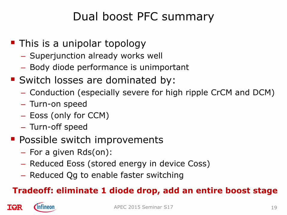
Dual boost PFC summary
This is a unipolar topology
– Superjunction already works well
– Body diode performance is unimportant
Switch losses are dominated by:
– Conduction (especially severe for high ripple CrCM and DCM)
– Turn-on speed
– Eoss (only for CCM)
– Turn-off speed
Possible switch improvements
– For a given Rds(on):
– Reduced Eoss (stored energy in device Coss)
– Reduced Qg to enable faster switching
APEC 2015 Seminar S17 19
Tradeoff: eliminate 1 diode drop, add an entire boost stage
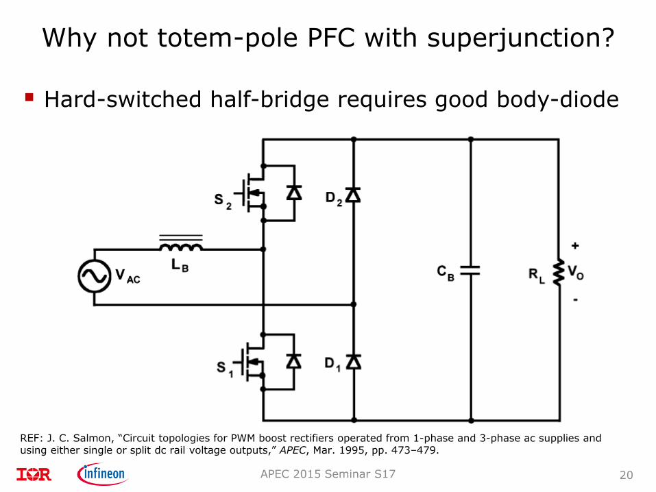
Why not totem-pole PFC with superjunction?
Hard-switched half-bridge requires good body-diode
APEC 2015 Seminar S17 20
REF: J. C. Salmon, “Circuit topologies for PWM boost rectifiers operated from 1-phase and 3-phase ac supplies and using either single or split dc rail voltage outputs,” APEC, Mar. 1995, pp. 473–479.
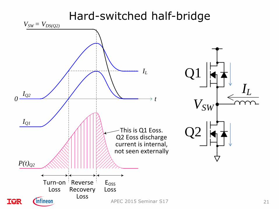
Hard-switched half-bridge
APEC 2015 Seminar S17 21
Q1
Q2
IL
VSW
IQ1
IQ2
VSW = VDS(Q2)
IL
0 t
P(t)Q2
Turn-on Loss
Reverse Recovery
Loss
EOSS
Loss
This is Q1 Eoss.Q2 Eoss discharge current is internal, not seen externally

Summary: topologies with limited superjunction use
Bipolar current flow topologies
– Anywhere diode recovery is important
Half-bridge hard-switching
– Totem-pole bridgeless boost CCM (except line polarity switch)
– Inverters, motor drives
Half-bridge soft-switching or resonant? Depends…
– Limited frequency range
– Risk of hard-switching
– Frequency dependent losses in Qoss
APEC 2015 Seminar S17 22

GaN High Electron Mobility Transistor (HEMT)
Depletion-mode basic HEMT
– Normally-on is a problem for power electronics
2 methods to achieve normally-off
– Cascode
– Enhancement-mode
GaN cascode characteristics
GaN enhancement-mode characteristics
GaN application summary
– Hard-switching
– Soft-switching & resonant
APEC 2015 Seminar S17 23

GaN High Electron Mobility Transistor (HEMT)
Depletion-mode (normally-on) HEMT
Si substrate for low cost
Normally-on potential problem for power electronics
APEC 2015 Seminar S17 24
Ref: Jones, E.A.; Wang, F.; Ozpineci, B., "Application-based review of GaN HFETs," Wide Bandgap Power Devices and Applications (WiPDA) 2014, pp.24-29, 13-15 Oct. 2014

Depletion-mode HEMT
Normally-on
– Essentially a resistor that can be turned-off with -gate bias
– Potential issues with power-up and power-down
– Requires additional master enable switch
– Requires negative gate drive
Low area specific on-resistance
Bi-directional conduction
– No intrinsic body diode
Can be made bi-directional blocking
Lateral device – monolithic integration possibilities
APEC 2015 Seminar S17 25

Cascode Provides Normally-OFF Function
Native d-mode GaN HEMT + LV Si FET in cascode
– Rds(on) is compromised to shift threshold positive
Cascode has easy gate drive
Cascode includes excellent body diode
2-chip solution no more difficult than IGBT
Almost zero “Miller Effect”
– C dv/dt immunity
– Enables turn-off ZVS in almost any topology
APEC 2015 Seminar S17 26
D
S
G
Low Voltage Si MOSFET
Depletion-Mode GaN HEMT
Hybrid Semiconductor Device, US Pat. 8,017,978 Hybrid semiconductor device having a GaN transistor and a Silicon MOSFET, US Pat. 8,368,120
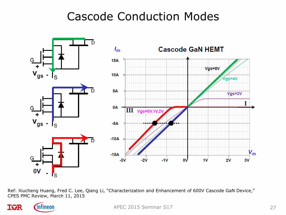
Cascode Conduction Modes
APEC 2015 Seminar S17 27
Ref: Xiucheng Huang, Fred C. Lee, Qiang Li, “Characterization and Enhancement of 600V Cascode GaN Device,” CPES PMC Review, March 11, 2015

Body diode reverse-recovery
>100x lower Qrr for GaN cascode
APEC 2015 Seminar S17 28
GaN cascode switch
Superjunction
10 A/div

Comparing GaN cascode to superjunction
1st Generation GaN cascode
APEC 2015 Seminar S17 29
Parameter GaN cascode Equivalent SJ
Package 6x8 mm PQFN 8x8 mm PQFN GaN 25% smaller package
Vdss 600 V 650 V
Rdson typ 25°C 135 mΩ 115 mΩ
Rdson typ 125°C 225 mΩ 230 mΩ GaN 1.67x; SJ 2x
Qg (10V Vgs, 480V Vds) 8.8 nC 35 nC GaN ~4X lower than SJ
Qrr (100A/µs, 25°C) 49 nC 6,400 nC GaN >100X lower than SJ
Coss (400V) 47 pF 53 - 579 pF Energy vs time equivalent
Rθ J-C (°C/W) 1.65 1.22 Consistent with package

Turn-on waveform, 135 mΩ (typ) cascode
Hard-switching Rg = 2Ω. ~9 µJ EON
APEC 2015 Seminar S17 30
5 A/div
Vds 100 V/div
Vgs 10 V/div

GaN HEMT Safe Operating Area
APEC 2015 Seminar S17 31
Measured destruct current >2x higher than calculated thermal limit
Lines represent calculated thermal limit – points are measured failures
Experimental data from 190 mΩ max cascode prototype 0.1
1
10
100
Dra
in C
urr
en
t, I D
(A
)
Drain-Source Voltage, VDS (V)
10 ms
1 ms
100 μs

GaN performance interdependent on package
APEC 2015 Seminar S17 32
Two key factors for minimizing losses:
– Minimize GaN – Si interconnect inductance
– Eliminate common-source inductance with Kelvin connection
REF: Z. Liu, X. Huang, FC Lee, Q. Li, “Investigation of Package Influence on High Voltage Cascode GaN HEMT with Simulation Model,” CPES review 2-13-2013, Milpitas, CA

Die-on-die cascode construction
Minimizes parasitic impedance between HEMT and FET
– Faster switching transitions, less ringing and overshoot
APEC 2015 Seminar S17 33
US Pat. No. 8,847,408
GaN on Si HEMT die
LV Si MOSFET mounted on Source pad of GaN on Si die
D
S
G
Low Voltage Si MOSFET
Depletion-Mode GaN HEMT

E-mode GaN HEMT Structures
a) P-gate enhancement-mode
b)P-gate enhancement-mode (gate injection)
APEC 2015 Seminar S17 34
Ref: Jones, E.A.; Wang, F.; Ozpineci, B., "Application-based review of GaN HFETs," Wide Bandgap Power Devices and Applications (WiPDA) 2014, pp.24-29, 13-15 Oct. 2014

Enhancement-Mode HEMT (Gate Injection)
APEC 2015 Seminar S17 35
Ref: http://www.semicon.panasonic.co.jp/en/news/contents/2013/apec/panel/APEC2013_GaN_FPD_WEB.pdf
off

Gate Characteristics (Enhancement Mode)
Typical non-insulated gate characteristic
– Gate injection uses small DC current (e.g. 10 mA)
APEC 2015 Seminar S17 36
Ref: Jones, E.A.; Wang, F.; Ozpineci, B., "Application-based review of GaN HFETs," Wide Bandgap Power Devices and Applications (WiPDA) 2014, pp.24-29, 13-15 Oct. 2014

Output Characteristics (Enhancement Mode)
HEMT turns back ON when drain goes below G, S
APEC 2015 Seminar S17 37
Ref: Jones, E.A.; Wang, F.; Ozpineci, B., "Application-based review of GaN HFETs," Wide Bandgap Power Devices and Applications (WiPDA) 2014, pp.24-29, 13-15 Oct. 2014

Reverse Bias Diode-Like Behavior
APEC 2015 Seminar S17 38
Vg1+
-
Vg2+
-
S
GD
S
GD
S’G
D’
VGS’ = VD’S’
S’ = drain acting as source in reverse biasD’ = source acting as drain in reverse bias
Equivalent Circuit when Vg = 0

Forward and Reverse I-V Characteristics
HEMT eventually saturates at very high current
APEC 2015 Seminar S17 39
Ref: http://www.semicon.panasonic.co.jp/en/news/contents/2013/apec/panel/APEC2013_GaN_FPD_WEB.pdf

GaN, superjunction, (& SiC) transfer curves
Cascode superjunction and SiC ~135 mΩ typical
E-mode GaN (non GIT) ~50mΩ (135 mΩ @ 150°C)
APEC 2015 Seminar S17 40
0.01
0.1
1
10
0 2 4 6 8 10
ID (
A)
VGS (V)
Transfer curve
SiC E-mode GaN
Cascode GaN
SJ

Comparing GaN vs SJ Qoss
APEC 2015 Seminar S17 41
REF: M. Treu, E. Vecino, M. Pippan, O. Häberlen, G. Curatola, G. Deboy, M. Kutschak, U. Kirchner,” The role of silicon, silicon carbide and gallium nitride in power electronics,” IEEE International Electron Devices Meeting, December, 2012
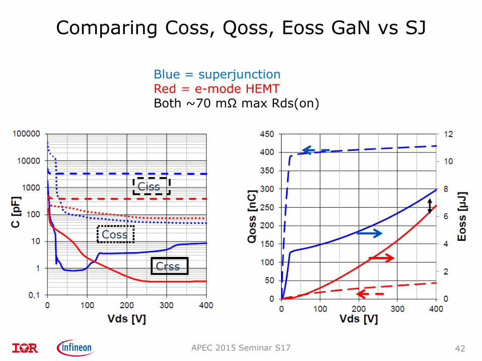
Comparing Coss, Qoss, Eoss GaN vs SJ
APEC 2015 Seminar S17 42
Blue = superjunction Red = e-mode HEMT Both ~70 mΩ max Rds(on)
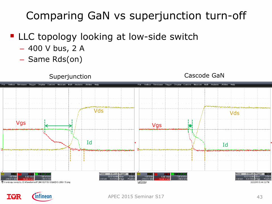
Comparing GaN vs superjunction turn-off
LLC topology looking at low-side switch
– 400 V bus, 2 A
– Same Rds(on)
APEC 2015 Seminar S17 43
Superjunction Cascode GaN
Vgs
Vds
Id
Vgs
Vds
Id

Avalanche and overvoltage
Superjunction has junction with avalanche capability
– Useful in circuits with unclamped inductive energy (flyback)
GaN has no junction, no avalanche behavior
– GaN ultimately breaks down destructively at ~2x rating
– Overvoltage spikes are allowed depending on supplier
GaN is best suited for half-bridge topology
– Fast body diode helps to mitigate overvoltage spikes
– Overvoltage spikes are clamped to bus
– With proper design, no risk of breakdown
APEC 2015 Seminar S17 44
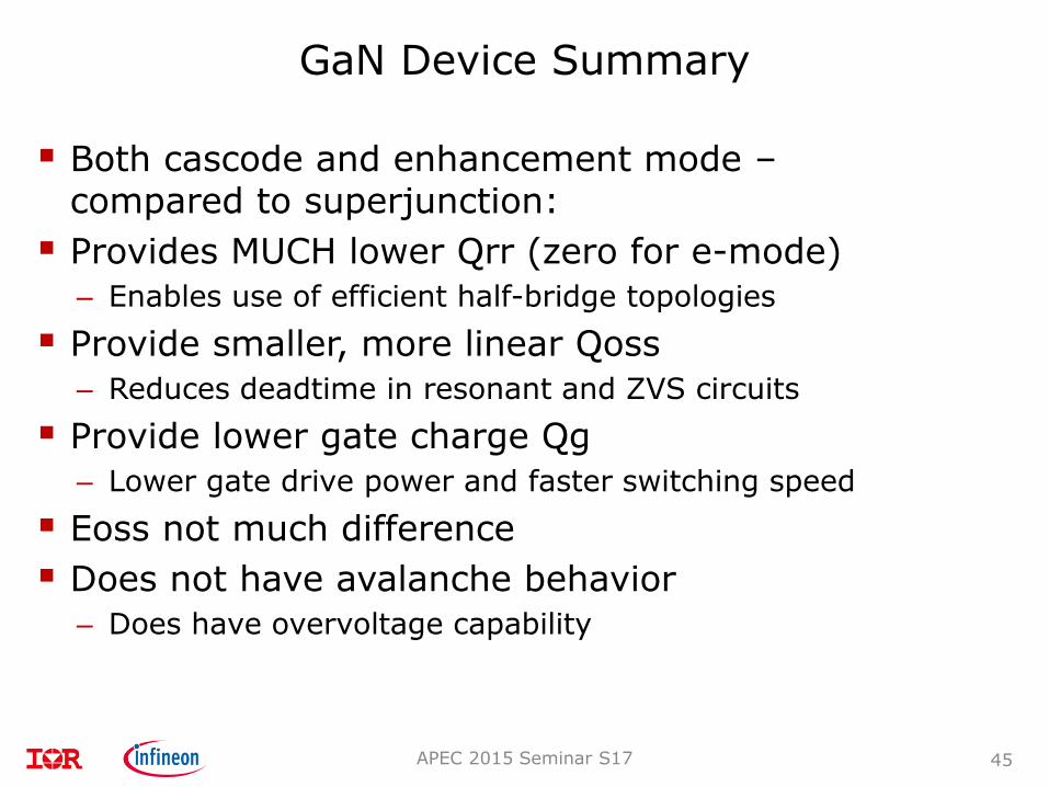
GaN Device Summary
Both cascode and enhancement mode – compared to superjunction:
Provides MUCH lower Qrr (zero for e-mode)
– Enables use of efficient half-bridge topologies
Provide smaller, more linear Qoss
– Reduces deadtime in resonant and ZVS circuits
Provide lower gate charge Qg
– Lower gate drive power and faster switching speed
Eoss not much difference
Does not have avalanche behavior
– Does have overvoltage capability
APEC 2015 Seminar S17 45

Applications of GaN
APEC 2015 Seminar S17 46

Gate Drive
Cascode – standard Si gate drivers work
– Vgs(th) is potential issue
– Common Source Inductance is a concern as always
– C dv/dt induced gate currents
– Kelvin gate-source connections
– Advantages of floating gate drive
APEC 2015 Seminar S17 47

Gate drive challenges for low threshold devices
Common Source Inductance distorts Vgs
Kelvin source connection eliminates CSI
…BUT can cause system grounding problems for driver
APEC 2015 Seminar S17 48
DC Bus
L
Isolated
DC Bus
L
Isolated
?

Isolated gate drive + Kelvin source connection
APEC 2015 Seminar S17 49
DC Bus
L
Isolated
?
DC Bus
L
Iso
late
d
Isolating both high and low-side drivers solves system ground bounce issues which can affect current sense and logic ground

Gate drive for gate injection
APEC 2015 Seminar S17 50
REF: T. Morita, H. Hanada, S Ujita, M Ishida, T. Ueda, “99.3% Efficiency Boost-up Converter for Totem-pole Bridgeless PFC Using GaN Gate Injection Transistors,” Proc. PCIM Europe, 20-22 May 2014

Gate drive summary
Cascode GaN:
– Standard FET gate driver compatibility
– Lower Qg for given current-handling capability
– ZVS turn-off easier to achieve
Enhancement-mode GaN
– Low threshold, noise sensitivity, negative drive can help
– Tighter limits on Vgs
– Very low Qg
– Kelvin source connection mandatory
– Floating driver helpful especially at higher power
APEC 2015 Seminar S17 52

Totem-Pole PFC Full-Bridge
APEC 2015 Seminar S17 53
ACLINE
EMI Filter
High Frequency Half-Bridge
60Hz Polarity Switch
DC Bus
Q1
Q2
Q3
Q4
This half-bridge is superjunction
This half-bridge is GaN cascode

Totem-Pole PFC Full-Bridge
2.5 kW all SMD power stage proof-of-concept
GaN boost stage 70 mΩ max enhancement-mode
superjunction sync line rectifiers
APEC 2015 Seminar S17 54
Bottom View of PCB
GaN
GaN Superjunction
EMI Filter
Q1
Q2
Q3
Q4
Superjunction

Totem-Pole PFC Full-Bridge
Input 230 VAC
Output 400 VDC, 6.25 A
CCM 45 to 65 kHz
APEC 2015 Seminar S17 55
Output EMI filter + Bus Capacitors
Heatsink
Input EMI filter Control board Aux power supply
PFC Inductor
Input
Output FAN

Totem-Pole PFC full-bridge performance
>99% efficiency from 18-70% load
APEC 2015 Seminar S17 56
98.2
98.4
98.6
98.8
99.0
99.2
99.4
0 500 1000 1500 2000 2500 3000
Effi
cien
cy (
%)
POUT (W)
Measured Efficiency - PFC, VIN=230VAC
Complete Power Stage. Vin=230 V, Tamb=25° C
45kHz
65kHz

Totem Pole PFC
No diode drops – only switch conduction voltage
Very high efficiency possible >99%
Lower component count than other bridgeless topologies
Topology is enabled by GaN HEMT
– Traditional Si FETs have too much body-diode Qrr Large recovery currents and high losses
Topology is Intrinsically bi-directional power flow
– Can also be used in inverter/UPS applications
APEC 2015 Seminar S17 57

Totem Pole PFC Future
MHz ZVS – still achieving 99% efficiency
Multiphase architectures to minimize ripple
Digital control to optimize performance & efficiency
APEC 2015 Seminar S17 58
Ref: Zhengyang Liu, Fred C. Lee, QiangLi, “Digital Control for MHz Totem-pole PFC Rectifier,” CPES PMC Review, Mar.11, 2015

LLC Resonant DC-DC
Popular topology today using superjunction
Frequency range <200 kHz typically
Caution required to prevent hard-switching
APEC 2015 Seminar S17 59

LLC typical waveforms and circuit
APEC 2015 Seminar S17 60

GaN enables shorter deadtime vs SJ @ 1MHz
Shorter deadtime lowers rms current
APEC 2015 Seminar S17 61
I2 Primary I2 Secondary Gate Drive
GaN 3.84A2 48.0A2 0.24W
Superjunction 4.93A2 64.6A2 1.88W
Difference +28.3% +34.6% +685%
SJ FET GaN Vds
Vgs
iprim
icentertap
80ns dead time 200ns dead time

Nonlinear Qoss Charge Affects Deadtime
APEC 2015 Seminar S17 62
0
50
100
150
200
250
300
350
400
450
500
0 10 20 30 40 50 60 70 80 90 100 110 120 130 140 150
Vo
lts
Time (µs)
3.3X longer charge-up time
Qoss Measurement Circuit

Cascode Charge Balance During ZVS Turn-ON
Improper charge balance results in loss of ZVS
Significant energy loss
Properly balanced Cascode achieves full ZVS
No energy loss
APEC 2015 Seminar S17 63
IL
Vsw
VDS-Si
X. Huang, W. Du, Z. Liu, F. C. Lee, and Q. Li, “Performance Analysis of Cascode GaN Device,” CPES Review, Nov 18, 2013
Measured Results: IR-Infineon Cascode

Cascode Charge Balance During ZVS Turn-OFF
Improper charge balance results in Si avalanche
Significant energy loss
Properly balanced Cascode no avalanche, full ZVS
No energy loss
APEC 2015 Seminar S17 64
X. Huang, W. Du, Z. Liu, F. C. Lee, and Q. Li, “Performance Analysis of Cascode GaN Device,” CPES Review, Nov 18, 2013
IL
Vsw
VDS-Si
Avalanche
Measured Results: IR-Infineon Cascode

ZVS phase-shifted full-bridge
ZVS over most of power range except light-load
Current-doubler output effective for 12 V and below
APEC 2015 Seminar S17 65

ZVS phase-shifted full-bridge
1 kW 380 V to 12 V
350 kHz
120 W/in3
APEC 2015 Seminar S17 66

ZVS phase-shifted full-bridge
Waveforms at 50% load
APEC 2015 Seminar S17 67

ZVS phase-shifted full-bridge efficiency
APEC 2015 Seminar S17 68
89
90
91
92
93
94
95
96
97
0 10 20 30 40 50 60 70 80 90 100
LOAD in % (1000W max)
Efficiency vs Percentage Load
380V to 12V fsw = 350 kHz
Load Efficiemcy
10% 89.5%
20% 94%
40% 96.1%
50% 96.4%
80% 96.3%
100% 95.7%

Efficiency vs Frequency at half-load
Comparing GaN cascode vs superjunction
APEC 2015 Seminar S17 69
93.5
94
94.5
95
95.5
96
96.5
97
0 100 200 300 400 500
Efficiency
freq[Khz]
GaN efficiency
SJ efficiency
Freq [Khz]
Efficiency_GaN [%]
Efficiemcy_SJ [%]
100 96.7 96.5
200 96.5 96.2
300 96.4 95.4
350 96.3 95
400 95.9 94
450 95.6
500 95.4

Why GaN for Motor Drive Applications?
Switching speed is not necessarily a key issue for drives:
Typically want dv/dt <6V/ns (GaN can switch >10x faster) – I=C dv/dt currents in motor windings can result in failures
– Corona and partial-discharge creates ozone and erodes insulation
– Common-mode currents forced through bearings, eroding races
Yet customers still want higher efficiency, increased density
Compressor drives have even more constraints: – Very low leakage current mandates small Y-cap values (EMI)
– Newer “green” refrigerants have very high permittivity
Goal is to improve light-load efficiency (<25% of full power)
EU2013 directive for Energy Saving A+++ Class
Reducing losses also improves packaging density
APEC 2015 Seminar S17 70

Typical Compressor Drive Today
APEC 2015 Seminar S17 71
EMI FILTER
LINEINPUT
BIAS POWER SUPPLY
GATEDRIVERS
ACMOTOR
INPUT RECTIFIER
DC BUS CAP
OUTPUT INVERTER
CONTROL & PWM

Conduction Voltage for Same Footprint Size
APEC 2015 Seminar S17 72
-3.0
-2.5
-2.0
-1.5
-1.0
-0.5
0.0
0.5
1.0
1.5
2.0
2.5
3.0
-5 -4 -3 -2 -1 0 1 2 3 4 5
Vd
s o
r V
ce (
Vo
lts)
Drain or Collector current (Amps)
Comparing Conduction voltage of IGBT vs FET (measured data)
IRGR4045D
0.8Ω Si
0.16Ω GaN
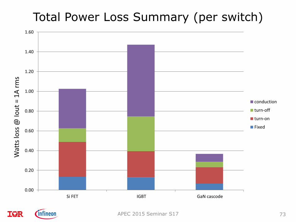
Total Power Loss Summary (per switch)
APEC 2015 Seminar S17 73
0.00
0.20
0.40
0.60
0.80
1.00
1.20
1.40
1.60
Si FET IGBT GaN cascode
conduction
turn-off
turn-on
Fixed
Wat
ts lo
ss @
Iou
t =
1A
rm
s

Cascode GaN dv/dt control via Gate Modulation
APEC 2015 Seminar S17 74
Vgs
Vsw
Vgs
Vsw
2A Turn off 2A Turn on
3.3V/ns 3.7V/ns
50ns/div 100ns/div
Dv/dt control possible by modulating cascode gate-drive current
This places HEMT in linear region increasing switching times and losses
Unknown if this affects long-term reliability – further study needed

GaN HEMT Short-Circuit Capability
Initial devices are high-gain – limited SCSOA
– Typically ~ 1 µs @ 300V
Likely tradeoff between gain and SCSOA similar to IGBTs
APEC 2015 Seminar S17 75
Ref: Xing Huang; Dong Young Lee; Bondarenko, V.; Baker, A.; Sheridan, D.C.; Huang, A.Q.; Baliga, B.J., "Experimental study of 650V AlGaN/GaN HEMT short-circuit safe operating area (SCSOA)," Proc. ISPSD pp.273,276, 15-19 June 2014

Summary
GaN HEMTs offer performance improvements for power electronic applications
– Benefits are strongly topology-dependent
– Just dropping GaN into existing circuit may show little benefit
Half-bridge topology is good match for GaN
– Half-bridge requires good dynamic reverse conduction
– Both cascode and e-mode GaN devices benefit half-bridge
Higher efficiency at same frequency
– By use of better topologies i.e. totem-pole PFC
Higher frequency at high efficiency
– Lower charge of GaN helps HF performance
– E.g. LLC example and ZVS full-bridge example
APEC 2015 Seminar S17 76

Questions?

References
1) Alex Lidow, Johan Strydom, Michael de Rooij, David Reusch, “GaN Transistors for Efficient Power Conversion, 2nd Edition,” Wiley, ISBN: 978-1-118-84476-2, Sept. 2014
2) Fedison, J.B.; Fornage, M.; Harrison, M.J.; Zimmanck, D.R., "Coss related energy loss in power MOSFETs used in zero-voltage-switched applications," APEC 2014, pp.150-156, 16-20 March 2014
3) Strydom, J.T.; van Wyk, J.D.; Ferreira, J.A., "Capacitor measurements for power electronic applications," IEEE IAS „99, vol.4, pp.2435,2440, 1999
4) Jones, E.A.; Wang, F.; Ozpineci, B., "Application-based review of GaN HFETs," Wide Bandgap Power Devices and Applications (WiPDA) 2014, pp.24-29, 13-15 Oct. 2014
5) Zhan Wang; Honea, J.; Yuxiang Shi; Hui Li, "Investigation of driver circuits for GaN HEMTs in leaded packages," Wide Bandgap Power Devices and Applications (WiPDA) 2014, pp.81-87, 13-15 Oct. 2014
6) Lautner, J.; Piepenbreier, B., "Impact of current measurement on switching characterization of GaN transistors," Wide Bandgap Power Devices and Applications (WiPDA) 2014, pp.98-102, 13-15 Oct. 2014
7) Chang-Yeol Oh; Yun-Sung Kim; Won-Yong Sung; Nam-Jin Cho; Byoung-Kuk Lee, "Analysis of MOSFET failure modes in bi-directional phase-shift full-bridge converters," APEC 2014, pp.43-48, March 2014
8) Xiucheng Huang, Fred C. Lee, Qiang Li, “Characterization and Enhancement of 600V Cascode GaN Device,” CPES PMC Review, March 11, 2015
9) Xing Huang; Dong Young Lee; Bondarenko, V.; Baker, A.; Sheridan, D.C.; Huang, A.Q.; Baliga, B.J., "Experimental study of 650V AlGaN/GaN HEMT short-circuit safe operating area (SCSOA)," Proc. ISPSD pp.273,276, 15-19 June 2014
APEC 2015 Seminar S17 78