Embed Size (px)
Citation preview

www.eecatalog.com/fpga 1
www.eecatalog.com/digital-signage
VP/PublisherClair Bright [email protected](415) 255-0390 ext. 15
EditorialEditorial DirectorJohn Blyler [email protected](503) 614-1082
Senior EditorChris A. [email protected]
EditorCheryl Berglund Coupé [email protected]
Creative/ProductionProduction ManagerSpryte Heithecker
Media CoordinatorJenn Burkhardt
Graphic DesignersNicky JacobsonJacob Ewing
Senior Web DeveloperMariam Moattari
Advertising/Reprint SalesVP/Publisher Embedded Electronics Media GroupClair Bright [email protected](415) 255-0390 ext. 15
Sales ManagerMichael Cloward [email protected] (415) 255-0390 ext. 17
Marketing/CirculationJenna Johnson
To Subscribewww.eecatalog.com/subscribe
Extension Media, LLCCorporate Office(415)255-0390
President and Group PublisherVince [email protected]
Vice President, Sales Embedded Electronics Media GroupClair [email protected]
Vice President, Business DevelopmentMelissa [email protected]
(415)-970-19100
Special Thanks to Our Sponsors
The Engineers’ Guide to PCI Express Solutions is published by Extension Media LLC. Extension Media makes no warranty for the use of its products and assumes no responsibility for any errors which may appear in this Catalog nor does it make a commitment to update the information contained herein. The Engineers’ Guide to PCI Express Solutions is Copyright ®2012 Extension Media LLC. No information in this Catalog may be reproduced without expressed written permission from Extension Media @ 1786 18th Street, San Francisco, CA 94107-2343.All registered trademarks and trademarks included in this Catalog are held by their respective companies. Every attempt was made to include all trademarks and registered trademarks where indicated by their companies.
Engineers’ Guide to FPGA and PLD Solutions 2013Welcome to the 2013
Engineers’ Guide to FPGA and PLD Solutions
It’s an exciting time for engineers who are designing and developing with programmable logic devices. New technologies offer tremen-dous jumps in performance – along with complexity. As usual, we bring you insight directly from experts in the field to help you antici-pate and address these new challenges.
Mentor Graphics shows “Six Ways Synthesis Can Support Design Assurance in FPGAs,” while Saelig Co. and Byte Paradigm explain “Working with Quad and Other SPI Protocols” and Loring Wirbel addresses verification tools in “FPGA Verification Must Address User Uncertainty for Prototyping, System Validation.”Jake Janovetz describes an evolutionary change in a particular FPGA applica-tion in “Machine Vision – Making the Leap from Frame Grabbers to FPGAs.” We also bring you the latest market and technology trends from Richard Wawrzyniak, senior analyst at Semico Research, in “Bandwidth Demands Drive FPGA/PLD Market.” Not surprisingly, our virtual roundtable discussion also focuses on new technolo-gies; you won’t want to miss “Move to 28nm Brings Opportunities and Challenges.”And for more detail on this exciting advance, Xilinx offers some final thoughts in “28nm—FPGAs Lead the Way in Semi-conductor Innovation & Value.”
Of course, that’s not all – this issue is full of product news, datasheets, events and other resources to keep you up to date with the latest in programmable logic. As always, we’d love to hear your feedback, thoughts and comments. Send them to [email protected].
Cheryl Berglund CoupéEDITOR
TO BEUPDATED

2 Engineers’ Guide to FPGA and PLD Solutions 2013
TOC

www.eecatalog.com/fpga 3
Special feature
Most hardware and software designers end up dealing with FPGAs in some way or another. Either the system they’re working on incor-porates one or more FPGAs and they have to write code or create logic to deal with them, or they simulate hardware behavior using a functionally-accurate simulator based upon FPGA reprogrammable logic. Because of this familiarity, many taken-for-granted FPGA tru-isms - let’s call them “laws of FPGA nature” - go unchallenged. We’re going to debunk a few of them here.
For example, designers assume that FPGAs always get bigger, denser and more expensive. Or that coding one up requires a mystical knowl-edge of C, HSPICE, HDL, RTL, and TLC finesse. It’s also a given that FPGAs are power hogs and are incapable of being used in low power designs like mobile handsets or tablet computers or the ultimate mobile device - your car. On the other hand, FPGAs are so flexible - essentially a blank sea of gates canvas - that low levels of abstraction (LUTS, MUXES, crossbars, NAND gates and so on) are fundamental building blocks that take huge effort to form into complex logic like processors, interface drivers, or MPEG decoders.
To answer these questions and more for this issue’s Roundtable Q&A, we turned to two of the biggest names in the business: Lattice and Xilinx. While it might seem a better match would be found between Altera and Xilinx, everyone lumps A and X together. Let’s face it, they play leapfrog all the time and their product lines are materially similar at the high density end of the market. Lattice, on the other hand, is more PLD-like and focuses at the cost-effective end of the market (Figure 1). However, Lattice remains surprisingly similar in capability to companies like Xilinx in hard logic integration, IP, EDA tool suites, and target markets. In fact, Lattice probably has a better chance of deploying FPGAs in smartphones, while Xilinx is really close to shipping Zynq-7000 SoCs into cars.
Lattice and Xilinx weigh in on the same set of questions, and their answers are at times in lockstep (IP, tools) or at opposite ends of the market (partial reconfiguration). Together, our experts offer a fabu-lous overview of the market from small- to high-density FPGAs.
EECatalog: Let’s face it, designing FPGAs is difficult and requires special knowledge, tools, and a mindset different from either coding or hardware layout. Yet the FPGA, PLD, and EDA vendors are improving tool suites all the time. What are some of the latest advances and what are some of the ones designers still are clamoring for?
According to Mike Kendrick, Director of Soft-ware Marketing, Lattice Semiconductor: There have been solid advances in providing designers pre-built functional blocks that speed up their design entry, design verification and timing closure tasks. For the foreseeable future, the HDL design flow continues to be the best alternative for users engaged in lower density programmable logic designs, as it gives them
the control they need to hit their aggressive cost and performance targets. In larger density designs, HW/SW co-design flows, where functionality can be moved easily between SW and HW, have the promise of moving system cost/performance to an entirely new level. However, these flows will take a long time to perfect, and will require users to acquire new skills. The more immediate need, where the processor is integrated on-chip with the FPGA, is a new class of cross-domain debugging tools to provide the visibility and control that embedded designers expect from their current discrete processor solutions.
Responds David Myron, Xilinx director of Platform Technical Marketing: Answer in a word…productivity. Productivity lowers our customers’ costs and enables them to get their end products to market faster, next generation design tools are focusing on what we consider the two pillars of productivity: integration and implementation.
The first pillar entails integrating a variety of IP from multiple domains, like algorithmic IP written in C/C++ and System C, RTL level IP, DSP blocks, and connectivity IP. Not only must this IP be integrated successfully, but it must be verified quickly—as individual blocks and as an entire system. For integration of differing types of IP, for example, the latest integration solutions provide an interac-tive environment to graphically connect cores provided by third parties or in-house IP using interconnect standards such as AMBA-AXI4. With easy drag-and-drop integration at the interface level, these solutions can guarantee that the system is structurally correct by construction through DRC checks.
The second pillar involves the capability of implementing multi-mil-lion logic cell designs for optimal quality-of-results in the shortest time possible. Because designs continue to increase in size and
Fundamental Laws of (FPGA) Nature: Similar, Yet Different Lattice and Xilinx muse on parallelism, partial reconfigurability, and the state-of-the-art in IP and EDA tools.
By Chris A. Ciufo, Senior Editor

4 Engineers’ Guide to FPGA and PLD Solutions 2013
Special feature
complexity, next generation solutions are now using single, scalable data models throughout implementation to provide users insight into design metrics such as timing, power, resource utilization, and routing congestion early in the implementation process. With up to a 4x productivity advantage over traditional development environ-ments, the Xilinx Vivado Design Suite attacks these four (4) major bottlenecks in programmable systems integration and implementation.
For instance, design changes are inevitable but schedules are often inflexible. Tools are now allowing for small changes to be quickly processed by only re-implementing small parts of the design, making iterations faster after each change. The latest tools can take a placed and routed design, this allows a designer to make ECO changes such as moving instances, rerouting nets, or tapping registers to primary outputs for debug—all without needing to go back through synthesis and implementation.
EECatalog: Partial reconfiguration on-the-fly is something major FPGA vendors have been talking about for a while. What’s new?
David Myron, Xilinx: Partial reconfiguration technology allows dynamic modification of FPGA logic by downloading partial bit files without interrupting the operation of the remaining logic. Designers can reduce system cost and power consumption by fitting sophisticated applications into the smallest possible device. This has been particularly useful with our customers developing space applications, software defined radio, communications, video and automotive markets. Using space systems as an example, ‘upgrades’ via partial reconfiguration reduce non-volatile rad-hard memory requirements—an expensive and limited resource on in-flight sys-tems. Partial reconfiguration is available in the full line of 7 series FPGAs and Zynq-7000 SoCs, with new capabilities including dedi-cated encryption support and partial bitfile integrity checks.
Kendrick, Lattice: PROTF (Partial Reconfiguration On the Fly) has been an interesting area of research for many years. The latest advances by certain FPGA vendors, while showing solid progress,
still leave a lot of issues unresolved.
The primary obstacles to PROTF have always been more “design-flow” oriented than “silicon enablement” oriented. The “silicon enablement” challenge has been largely under-stood, and solved, for many years; however, it carries a significant silicon area overhead and so is not economically viable unless the customer’s designs actually leverage the PROTF capabilities. On the other hand, the “design-flow” challenges are quite substantial, and remain unsolved. As one of many examples, users will need a method to simulate (and debug) their design functioning during reconfigura-tion to ensure that their system level design is operating correctly. While certain vendors have recently demon-strated design flows that deploy PROTF when targeting a very narrow set of highly algorithmic, computationally intense problems, no one has demonstrated any capability to deliver such benefits to the design flow for “typical” digital logic systems.
EECatalog: FPGAs get bigger, denser, and more SoC-like. What is do-able today that was unheard of only 3 years ago?
Kendrick, Lattice: Not all FPGAs are getting bigger, and the market for lower density devices is growing. For example, while the breadth of densities that Lattice offers is increasing, we are more focused on creating the lowest cost, lowest power solution at a given density. For instance, our MachXO2 FPGA, despite its low cost and low power, includes hard logic for commonly used interfaces, including SPI and I2C. Our mixed signal Platform Manager product integrates analog circuits with programmable logic specifically to reduce the cost of power management within more complex systems. Our iCE40 FPGA uses an extremely small (and unique) non-volatile programming cell combined with an innovative programming architecture to enable a new low cost standard for programmable logic.
Myron, Xilinx: Access to “bigger” devices is a natural customer requirement. The “denser” devices, particularly All Programmable
Figure 1: Lattice Power Calculator tool, part of the company's Diamond Design Software suite.
Figure 2: Xilinx Vivado Design Suite IDE main screen.

www.eecatalog.com/fpga 5
Special feature
3D FPGAs, open more opportunities in test, measurement and emulation markets. The density and integration of the fabric—including CLBs, Block RAM and DSP blocks—allow performance levels that are not available in multi-chip solutions because of chip-to-chip delay.
SoC [FPGA] architectures such as Zynq alleviate multi-chip solu-tions, and have opened up new markets requiring high speed signal processing and real-time responsiveness. Having the complete processing system linked to the FPGA fabric allows architects to partition their design into software in the processing sub-system or accelerators in the FPGA fabric, all on one integrated chip.
EECatalog: The fastest growing markets on the planet deal with wireless connectivity. FPGAs have a strong play in the infrastruc-ture—but what’s required to get their power down enough to be deployed in the actual battery-powered embedded device? Does this affect other markets/systems as well?
Kendrick, Lattice: There are at least two distinct markets: the bandwidth-driven wireless infrastructure market and the power-driven mobile device market.
First, to answer whether FPGA power can be sufficiently reduced, it already has been. Our iCE40 and MachXO2 FPGA families achieve both mobile-friendly static power levels (~10-50µW) and consumer market-friendly costs (~$1.00 ASP).
Yes, there are significant tradeoffs required at every level of the ecosystem in order to develop products for one market versus the other. Fundamentally, one ecosystem is driven by high-speed switching, while the other is driven by low-power operation. With that in mind, the following tradeoffs must be made:
1. Speed/Power Process Tradeoff: The types of processes that are used to design bandwidth-driven infrastructure FPGAs have far too much static leakage power to also support mobile devices, while the processes that can support mobile devices with very low static leakage power have slightly slower transistors.
2. Design Tradeoff: Today many FPGAs are designed using NMOS pass gates in the routing fabric (for cost and speed), while low power mobile FPGAs must employ full CMOS pass gates in the routing fabric. One design cannot effectively support both markets.
3. Interface Standards: The infrastructure market demands very high-performance IOs – from high-speed SERDES (PCIe, etc.) to high speed memory interfaces (such as DDR3). The mobile market has a very different set of interface standards; for example, the MIPI Alliance is driving a new set of very low power IO interfaces such as D-PHY and M-PHY. So, the infrastructure and mobile ecosystems have very different IO interface require-ments and one design cannot effectively support both markets.
4. Package Requirements: The infrastructure market demands very high IO counts (typically ~400-800), which drive very large and expensive packages (currently flip-chip is the technology of choice while, most recently, 3D/TSV package technology is being developed). The mobile ecosystem is at the opposite end of the spectrum, where size and board space is at a premium. As a result, the focus here is on small packages (typically 2mm x
2mm) with fewer IOs (typically ~20-40) and aggressive ball pitch (typically 0.4mm) in order to maximize IO count while minimizing board footprint.
These two unique markets drive two fundamentally different FPGA solutions – and the differences exist at every level.
EECatalog: The two biggest features of FPGAs are parallelism and raw bandwidth/throughput. What’s new in these areas at the chip- and system-level?
Kendrick, Lattice: FPGAs certainly provide designers the ability to implement parallel algorithms, and thus increase a system’s throughput if this is applied to a bottleneck. Lattice, for example, provides a complete system building solution with our Lattice-Mico System Builder, and also unique to the industry the company provides a choice of both a 32-bit microprocessor and 8-bit microcon-troller. So, designers can quickly build custom platforms that have parallel engines, and marry that to the amount of serial processing power they need.
Myron, Xilinx: Communication protocols continue to require higher line rates and throughput from generation to generation. The latest devices provide up to 28 Gb/s transceivers, and soon we’ll see 32+ Gb/s and 56Gb/s transceivers to support next generation pro-tocols and beyond. Yet with higher line rates comes the challenge of ensuring high channel quality in the context of the system. As signals travel across a printed circuit board (PCB), the high-speed components of the signal get attenuated. This is why auto-adaptive equalization is imperative for transceivers—to automatically com-pensate for any channel-driven signal distortion. As an example, network line cards can be moved from slot to slot on a system’s back-plane while still maintaining high signal integrity-- despite the fact the channel lengths have changed. These auto-adaptive equalization solutions are already available in the Xilinx 7 series FPGAs and will be optimized further in our next generation devices.
Higher in-coming data flow requires greater parallelism and wider data busses inside the FPGA. Current FPGAs at 28nm handle the most aggressive requirements of today. To support next generation serial bandwidth requirements, improvements in both silicon and tool fabric are needed. Silicon fabric will need to be optimized across many architectural blocks, along with improvements in routing architecture to support as much as 90% device utilization, which is a challenge in the industry today. Furthermore, design tools need to be “co-optimized” with devices to ensure designers get maximum value. Next generation routing architectures in the silicon, for example, have to be coupled with advancements in routing algorithms in the tools.
Chris A. Ciufo is senior editor for embedded content at Extension Media, which includes the EECatalog print and digital publications and website, Embed-ded Intel® Solutions, and other related blogs and embedded channels. He has 29 years of embedded technology experience, and has degrees in electrical engineering, and in materials science, emphasizing solid state phys-ics. He can be reached at [email protected].

6 Engineers’ Guide to FPGA and PLD Solutions 2013
Special feature
This year’s Chip Design Trends (CDT) “ASIC/ASSP FPGA-based Prototyping” (2012) survey reinforced past trends while providing a few surprises. The survey yielded much data, so let’s start with a high-level overview.
In 2012, hardware-software co-design and co-verification were again the number-one reason for ASIC designers to use FPGA-based prototypes (see Figure 1). Not surprisingly, hardware chip verification was the second leading driver, followed by software and then system verification.
A surprise came when designers were asked about future planned projects. All of the above current motivators were still there. But respondents indicated that software devel-opment would fall behind IP development and verification as an important issue. This probably means that IP development and verification has proven to be a sore spot for today’s designers.
How do these trends for 2012 compare to years past? Hardware-software co-design and co-verification remain the biggest reason for the FPGA prototyping of ASICs, fol-lowed by hardware-chip verification (see Figure 2). In 2012, software development continues to climb as an important driver while system-integration issues fall. IP develop-ment and verification has mixed results, suggesting that this factor requires further investigation. I’ll try to cross-correlate the IP trend with other data in a future article.
John Blyler is the editorial director of Extension Me-dia, which publishes Chip Design and Embedded Intel® Solutions magazine, plus over 36 EECatalog Engineers’ Guides in vertical market areas.
What Drives ASIC Prototyping The latest results from the annual CDT survey point to changes in the reasons behind ASIC prototyping – from hardware, software, and systems to IP. with FPGAs in 2012 and Beyond?
By John Blyler, Editorial Director
Figure 1: Current and planned reasons why ASIC/ASSP chip designers use FPGA-based prototypes. Courtesy of Chip Design Trends (CDT)
Figure 2: Shown are cumulative reasons for FPGA prototyping – from 2008 through 2012. Courtesy of Chip Design Trends (CDT)

www.eecatalog.com/fpga 7
Special feature
In recent years, the automotive industry has made remark-able advances in driver assistance (DA) systems that truly enrich the driving experience and provide drivers with new forms of information about the roadway around them. This article looks at how FPGAs can be leveraged to quickly bring new driver assistance innovations to market.
Driver Assistance IntroductionSince the early 1990s, developers of advanced DA systems have envisioned a safer, more convenient driving experience. Over the past two decades, DA features such as ultrasonic park assist, adaptive cruise control and lane-departure warning systems in high-end vehicles have been deployed. Recently, automotive manufacturers have added rear-view cameras, blind-spot detection and surround-vision systems as options. Except for ultrasonic park assist, deployment volumes for DA systems have been limited. However, the research firm Strategy Analytics forecasts that DA system deployment will rise dramatically over the next decade, including growth from $170 billion in 2011 to $266 billion by 2016 – a compound average annual growth rate of 9.3%.
In addition to government legislation and strong consumer interest in safety features, innovations in remote sensors and associated processing algorithms that extract and inter-pret critical information are fueling an increase in DA system deployment. Over time, these DA systems will become more sophisticated and move from high-end to mainstream vehicles, with FPGA-based processing playing a major role.
Driver Assistance Sensing Technology TrendsSensor research and development activities have leveraged adjacent markets, such as cell phone cameras, to produce devices that not only perform in the automotive environment, but also meet strict cost targets. Similarly, developers have refined complex processing algorithms using PC-based tools and are transi-tioning them to embedded platforms.
While ultrasonic sensing technology has led the market, IMS Research (Figure 1) shows camera sensors dominating in the coming years.
A unique attribute of camera sensors is the value of both the raw and processed outputs. Raw video from a camera can be directly displayed for a driver to identify and assess
Driver Assistance Systems with the Power of FPGAs
By Paul Zoratti, Xilinx
Figure 1: Driver Assistance Sensors Market
Figure 2: Bundling Multiple Automotive Features
FPGAs can be leveraged to quickly bring new driver assistance innovations to market

8 Engineers’ Guide to FPGA and PLD Solutions 2013
Special feature
hazardous conditions, something not possible with other types of remote sensors (for example, radar). Alternatively (or even simultaneously), the video output can be processed using image analytics to extract key information, such as the location and motion of pedestrians. Developers can fur-ther expand this “dual-use” concept of camera sensor data by bundling multiple consumer features based on a single set of cameras, as illustrated in Figure 2.
From such applications, it is possible to draw a number of conclusions regarding the requirements of suitable pro-cessing platforms for camera-based DA systems:
• Theymust supportbothvideoprocessing and imageprocessing.In this case, video processing refers to proper handling of raw camera data for display to the driver, and image processing refers to the application of analytics to extract information (for example, motion) from a video stream.
• Theymustprovideparallel datapaths for algorithms associatedwith features that will run concurrently.
• Giventhatmanynewfeaturesrequiremegapixelimageresolution,connectivity and memory bandwidth are just as critical as raw processing power.
Meeting DA Processing Platform RequirementsFPGAs are well suited to meet DA processing platform requirements. For example, in a wide-field-of-view, single-camera system that incorporates a rear cross-path warning feature, the system’s intent is to provide a distortion-corrected image of the area behind the vehicle. In addition, object-detection and motion-estimation algo-rithms generate an audible warning if an object is entering the projected vehicle path from the side.
Figure 3 illustrates how the camera signal is split between the video- and image-processing functions. The raw pro-cessing power needed to perform these functions can quickly exceed what is available in a serial digital signal processor (DSP). Parallel processing along with hardware acceleration is a viable solution.
FPGAs offer highly flexible architectures to address various processing strategies. Within the FPGA logic, it is a simple matter to split the camera signal to feed independent video- and image-processing intellectual property (IP) blocks. Unlike serial processor implementations, which must time-multiplex resources across functions, the FPGA can execute and clock processing blocks independently. Additionally, if it becomes necessary to make a change in the processing architecture, the ability of the FPGA to reprogram hardware blocks surpasses solutions based on specialized application-specific standard products (ASSPs) and application-specific integrated circuits (ASICs), giving FPGA implementations a significant advantage when anticipating the future evolu-tion of advanced algorithms.
Another benefit of FPGA implementation is device scal-ability. As OEMs look to bundle more features, processing
needs will rise. For example, the rear-view camera might need to host a monocular ranging algorithm to provide drivers with information on object distance. The added functionality requires yet another parallel-processing path. Implementing this in a specialized ASIC or ASSP could be problematic, if not impossible, unless the designers made provisions for such expansion ahead of time.
Attempting to add this functionality to a serial DSP could require a complete re-architecture of the software design, even after moving to a more powerful device in the family (if it is plausible at all). By contrast, an FPGA-based imple-mentation allows the new functional block to be added, utilizing previously unused FPGA logic and leaving existing blocks virtually intact. Even if the new function requires more resources than are available in the original device, part/package combinations frequently support moving to a denser device (that is, one with more processing resources) without the need to redesign the circuit board or existing IP blocks.
Finally, the reprogrammable nature of FPGAs offers “silicon reuse” for mutually exclusive DA functions. In the rear-looking camera example, the features described are useful while a vehicle is backing up, but an FPGA-based system could leverage the same sensor and processing electronics while the vehicle is moving forward, with a feature such as blind-spot detection. In this application, the system analyzes the camera image to determine the location and relative motion of detected objects. Since this feature and its associated processing functions are not required at the same time as the backup feature, the system can recon-figure the FPGA logic within several hundred milliseconds based on the vehicle state. This allows the complete reuse of the FPGA to provide totally different functionality at very little cost.
Figure 3: Video and Image Processing Functions

www.eecatalog.com/fpga 9
Special feature
Meeting DA External Memory Bandwidth RequirementsIn addition to raw processing performance, camera-based DA applications require significant external memory access bandwidth. The most stringent requirements come from multi-camera systems with centralized processing, for example, a four-camera surround-view system. Assuming 4 megapixel imagers (1,280 x 960), 24-bit color processing, and performance of 30 frames per second (FPS), just storing the imagers in external buffers requires 3.6 Gb/s of memory access. If the images need to be simultaneously read and written, the requirement doubles to 7.2 Gb/s. With an 80 percent read/write burst efficiency, the requirement increases to 8.5 Gb/s. This estimate does not include other interim image storage or code access needs. With these requirements, it is clear that camera-based DA applications are memory bandwidth-intensive.
These systems also commonly require memory controllers; however, adding one in a cost-effective manner requires efficient system-level design. Again, developers can leverage the flexibility of the FPGA to meet this need. To summarize, FPGA memory controllers provide customized external memory interface design options to meet DA band-width needs and optimize all aspects of the cost equation (memory device type, number of PCB layers, etc.).
DA Image Processing Need for On-Chip Memory ResourcesIn addition to external memory needs, camera-based DA pro-cessing can benefit from on-chip memory that serves as line buffers for processing streaming video or analyzing blocks of image data. Bayer transform, lens distortion correction and optical-flow motion-analysis are examples of functions that require video line buffering. For a brief quantitative analysis, a Bayer transform function using 12-bit-pixel Bayer pattern intensity information to produce 24-bit color data is examined. Implemented as a raw streaming process, a bicubic interpolation process requires buffering four lines of image data. Packing the 12-bit-intensity data into 16-bit locations requires approximately 20.5 kb of storage per line, or 82 kb for four lines of data.
As part of their suite of on-chip resources, today’s FPGAs offer localized memory called Block RAM. The BRAM sup-ports line buffer storage of image data in close proximity to fabric-based image processing cores. As FPGAs now target vision applications, the relative amount of BRAM resources has increased with each product family.
A Single All-Programmable PlatformIn addition to external memory bandwidth requirements and image processing needs, having a single, all-programmable system on a chip (SoC)-based platform for DA applications offers automotive manufacturers the unique ability to address both the technical challenges and business goals in their DA designs. This type of all-programmable platform offers designers an integrated, flexible, power optimized solution with high computational performance that auto-
motive manufacturers and their electronics suppliers can combine with their own hardware and software, available IP and design frameworks to reduce development time, bill of material (BOM) costs and risk for next-generation DA solutions.
Currently, this type of platform has only been offered as a multi-chip solution, which can require additional pro-cessing that keeps BOM costs high, and reduces flexibility options to scale between vehicle platforms. Yet automotive designers can now take advantage of the industry’s first SoC family that incorporates an ARM dual-core Cortex-A9 MPCore processing system with tightly coupled program-mable logic on a single die. This combination dramatically increases performance, which is critical for processing-intensive real-time DA applications, and enable greater system integration, allowing the bundling of multiple DA application, while simultaneously reducing BOM costs by minimizing device cost and the cost of additional hardware platforms.
Automakers are eager to offer car buyers increasingly advanced DA applications, which have already proven to be quite popular in manufacturers’ high-end vehicles. By presenting new DA applications and being able to offer multiple DA applications per vehicle using an all program-mable, customized solution, automakers are now given the opportunity to differentiate their vehicles from those of their competitors in a hotly contested market.
Paul Zoratti is a member of the Xilinx Automotive Team. As a senior system architect and manager of driver assistance platforms, his primary responsi-bility is the global application of Xilinx technology to automotive driver assistance systems. Zoratti holds master’s degrees in both electrical engi-neering and business administration, both from the University of Michigan. He also has a specialized graduate certification in intelli-gent transportation systems, also from the University of Michigan. Zoratti has been awarded 16 United States patents associated with vehicle safety technology.

10 Engineers’ Guide to FPGA and PLD Solutions 2013
EECatalog Special Feature
Accelerating software by moving it to massively parallel hardware continues to develop as an attractive method-ology. The merit of hardware acceleration is significant, but there are hurdles that should be budgeted for.
To start, it’s important to understand that with hardware acceleration there are three primary forms of parallelism: 1) blocks of code that execute in parallel by splitting the data set into multiple parts; 2) pipelined (bucket brigade) blocks of code that operate on streaming data; and 3) hybrid parallelism that combines both forms.
On the merit side, each unrolling of a critical path loop into an independently streaming process can double wall-clock performance. Modern FPGAs, with several million usable (in contrast to advertised) gates can host a dozen or more independent streams. Accordingly, we are seeing solid 10x acceleration in “parallelizable” designs in appli-cation domains such as image processing, encryption and network filtering. The process is not trivial. While we have student groups from Rochester Institute of Technology to the University of Naples delivering remarkable speed ups, adoption by industry is concentrated among a few thou-sand classic early adopters.
This article covers the current state of the art on software to hardware compilation, provides some realistic tips, and suggests a vision of how to make it more usable by the next wave of developers.
FPGAs Explained for the Non-Hardware FolkMost software developers write code for microcontrollers or microprocessors. C remains the dominant language for design starts. CPUs and microcontrollers typically feature single or low number multiple-cores. They achieve throughput via increasing clock speeds but are constrained by having to share limited cores and common memory. Think of it as driving ever faster through a single or dual toll booth on a bridge.
FPGAs run at lower clock speeds than microprocessors. They achieve throughput by having very f lexible input and output, so non-sequential tasks can be designed into parallel processes. While a conventional processor only does one operation at a time, a properly engineered FPGA design will concurrently perform hundreds or thousands of operations. Most designs for FPGAs are developed using an HDL (hardware description language) like VHDL or Verilog. They are not particularly difficult languages
but are sufficiently arcane that C programmers do not gen-erally take to them. We have seen more cross-over from HDL engineers learning C than the other way around.
Gate count can be deceptive. Microprocessors use the available silicon with high efficiency. FPGAs can use a sig-nificant fraction of their gates for routing. And, you may not be certain of resource availability. FPGAs have great “blocks” of special purpose gates such as DSP, but they are limited. When you’re out of special blocks, you’re out, and the routing software will use less efficient gates, reducing performance and space efficiency.
Historically FPGAs are descendants of PALs, GALs and PLDs. These precursor devices were much smaller. The ear-liest ones were small enough to program in Assembly. The devices grew and the early HDLs emerged and improved. Design shifted to HDLs like Data I/O’s ABEL, MMI’s PALASM and others. Jump to today and the same shift is occurring. HDLs like VHDL and Verilog are more time con-suming but offer better control over resources. C to HDL to RTL (Register-transfer level: the gate level machine code that characterizes the FPGA) tools like Impulse C, ROCC, C2H, Vivado and others offer a higher level of abstraction but may not have the same QoR (Quality of results) initially. More about this later when we talk about the design flow.
Design FlowHigh Level Language, or HLL programming typically refers to C. System C, C#, C++ are all great languages with ardent users. But for this article we’re sticking with ANSI C, as most IP is created in this version of C.
From Visual Studio to FPGA HardwareA snapshot on the current state-of-the-art in FPGA software to hardware compilation.
By Brian Durwood, Co-founder, Impulse Accelerated Technologies; Nicola Granny, President, MNB Technologies
When you’re out of special blocks, you’re out, and the routing software will use
less efficient gates, reducing performance and space
efficiency.
www.eecatalog.com/fpga 11
EECatalog Special Feature
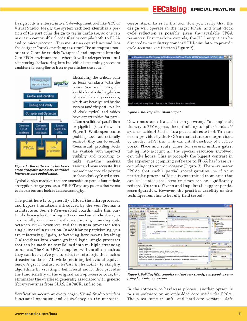
Design code is entered into a C development tool like GCC or Visual Studio. Ideally the system architect identifies a por-tion of the particular design to try in hardware, so one can maintain comparable C code files to compile both to FPGA and to microprocessor. This maintains equivalence and lets the designer “break one thing at a time”. The microprocessor-oriented C can be crudely “wrapped” and imported into the C to FPGA environment – where it will underperform until refactoring. Refactoring into individual streaming processes enables the compiler to better parallelize the code.
Identifying the critical path to focus on starts with the basics. You are hunting for key blocks of code, largely free of serial data dependencies, which are heavily used by the system (and they eat up a lot of clock cycles) and which have opportunities for paral-lelism (traditional parallelism or pipelining), as shown in Figure 1. While open source profiling tools are not fully realized, they can be useful. Commercial profiling tools are available with improved visibility and reporting to make run-time analysis easier and more accurate. It is not rocket science; the point is to chase clock cycle reduction.
Typical design modules that are amenable to parallelism include encryption, image processes, FIR, FFT and any process that wants to sit on a bus and look at data streaming by.
The point here is to generally offload the microprocessor and bypass limitations introduced by the von Neumann architecture. Some FPGA-enabled boards make this par-ticularly easy by including PCIe connections to host so you can rapidly experiment with partitioning… moving code between FPGA resources and the system processor with single lines of instruction. In addition to partitioning, you are refactoring. Again, refactoring here means breaking C algorithms into coarse-grained logic: single processes that can be machine parallelized into multiple streaming processes. The C to FPGA compilers will unroll as much as they can but you’ve got to refactor into logic that makes it easier to do so. All while retaining behavioral equiva-lency. A great feature of FPGAs is the ability to simplify algorithms by creating a behavioral model that provides the functionality of the original microprocessor code, but eliminates the overhead generally associated with generic library routines from BLAS, LAPACK, and so on.
Verification occurs at every stage. Visual Studio verifies functional operation and equivalency to the micropro-
cessor stack. Later in the tool f low you verify that the design will operate in the target FPGA, and what clock cycle reduction is possible given the available FPGA resources. Post machine compile, the HDL output can be directed to an industry standard HDL simulator to provide cycle accurate verification (Figure 2).
Now comes some leaps that can go wrong. To compile all the way to FPGA gates, the optimizing compiler hands off synthesizable HDL files to a place and route tool. This can be one provided by the FPGA manufacturer or one provided by another EDA firm. This can entail one heck of a coffee break. Place and route times for several million gates, taking into account all the special resources involved, can take hours. This is probably the biggest contrast in the experience compiling software to FPGA hardware vs. compiling it to microprocessor (Figure 3). There are newer FPGAs that enable partial reconfiguration, so if your particular process of focus is constrained to an area that can be isolated, the iterative times can be significantly reduced. Quartus, Vivado and Impulse all support partial reconfiguration. However, the practical usability of this technique remains to be fully field tested.
In the software to hardware process, another option is to run software on an embedded core inside the FPGA. The cores come in soft- and hard-core versions. Soft
Figure 1: The software to hardware stack generates necessary hardware interfaces post-optimization.
Figure 2: Desktop simulation output.
Figure 3: Building HDL: complex and not very speedy, compared to com-piling for a microprocessor.

12 Engineers’ Guide to FPGA and PLD Solutions 2013
EECatalog Special Feature
cores are programmed into general purpose gates. While FPGA-hosted processors are slower than those of the host machine, they are typically Harvard architecture with physically separate storage and signal pathways for instructions and data. This gives them a memory access advantage and direct communication with the FPGA logic, bypassing host to hardware overhead. Sometimes this can be a less efficient use of silicon, but multiple cores can be added as the design may need. Cores can be proprietary, provided by the FPGA vendor and useful if not familiar. Increasingly FPGA suppliers are standardizing on ARM cores. This trend is expected to continue. The use of cores in FPGAs as SoC (system on chip) solutions is an intrinsic benefit. The on-board core can consolidate microcontroller or light micro processing tasks on one chip.
Development environments such as Impulse CoDeveloper also interoperate with full-featured heavily used tools such as Microsoft™ Visual Studio. A practical example is provided in Impulse App Note 112 by Michael Kreeger “IATAPP-112”.
For example, while installing Impulse C and CoDeveloper the Visual Studio plug in is automatically installed and just has to be selected during setup. When Visual Studio is thereafter launched, the top pull down-down menu can be used to select “File->New Project…” which creates a sub directory for the new project. If beginning from existing code, those source files are copied into the solution direc-tory. Header and source files are added to the Visual Studio Project and then to the source files folder in the solution explorer directory. To verify before hardware gen-eration a “debug” software project is built, which makes it possible to test the application from desktop simulation. Next, select the hardware environment from the con-figuration manager to build the HDL for the target FPGA. This enables the synthesizable HDL to be exported to the appropriate place and route tool to generate RTL for the target FPGA. The whole process may take an hour or so.
As a new methodology this tends to be minimally disrup-tive. The pragmas and additions are pretty common sense.
Glitches may arise from “plumbing” (a whole different topic), such as getting things lined up with PCIe drivers, DMA, DDR and all the devilish details. Our two cents is that the growing body of known good examples and reference designs makes this process less risky. On the tool side we’d like to see shorter place and route times, better back annotation and more useful profiling. Overall as the FPGAs and FPGA based acceleration cards mature, and the body of available IP expands, this technique becomes more mainstream.
Brian Durwood co-founded Impulse Accelerated Technologies in 2002 with David Pellerin, a co-worker from the ABEL® days at Data I/O. Impulse has grown to be the most widely used C to FGPA tool, with customers from NASA to Detroit to Wall Street. Mr. Durwood was previously a VP at Tek-tronix, a VP at Virtual Vision and an Analyst at NBC. Mr. Durwood is a graduate of Brown and Wharton. Impulse now offers tools, IP and design/integration services.
Nick Granny is a scientist, engineer, and entrepre-neur who has been supporting the EDA and high-performance computing communities for more than 25 years. Currently Nick is co-founder and CEO of MNB Technologies, a small company that develops artificial intelligence-based EDA tools and provides technical services to the Impulse C user community. Prior to MNB, Nick was the lead staff scientist in Mentor Graphics research into FPGA-accelerated computing and was also a key member of the de-velopment and launch team for the IKOS/Mentor VirtuaLogic emu-lation system. Earlier in his career, Nick was an embedded systems engineering consultant to regional electric power utilities and the top-tier critical care medical apparatus manufacturers. Nick is a medically retired US Naval Officer and further serves his commu-nity as an adjunct computer sciences instructor and course develop-ment consultant to Indiana’s state-wide community college system.

www.eecatalog.com/fpga 13
Special feature
To address the insatiable demand for bandwidth, the communications industry is accelerating development of Nx100G line cards for networking systems. In order for equipment manufacturers to scale infrastructure eco-nomically and effectively, they must leverage the latest optical interconnect technologies such as CFP2, and in the future CFP4, to increase bandwidth while lowering power and cost.
By working with network developers, Xilinx anticipated this need and developed transceiver- rich, high-perfor-mance, programmable devices comprised of heterogeneous silicon die. The technology supports the required 28 gigabits per second (Gb/s) channels for CFP2 optics and delivers optimal signal integrity due to its heterogeneous architecture. With high logic capacity and specific IP for communications applications, these devices provide extensive levels of system integration to usher in the migration to next-generation optics.
Demand for BandwidthLargely driven by streaming video, HD video, cloud com-puting, and mobile networking, the consumer market’s relentless demand for network bandwidth compels the com-munications industry to double system capacity every three years. Service providers supporting the Internet’s backbone must lead the migration to 100G and 400G and stay at the forefront of the latest technologies and standards.
Service providers not only demand more bandwidth but aim to reduce capital and operating expenses. For equipment manufacturers, this means rolling out solutions with leaps in performance, area efficiency, and cost effectiveness over previous generation products.
The Move to Next-Generation Optics for Nx100GMost of today’s network infrastructure is connected via optical fiber, hence the bandwidth and cost of optical modules are major development considerations. The type of modules that can be used depends on the architecture of the application’s line cards. Three well known optical module standards include SFP+, CFP, and CFP2—each with varying throughput, cost per bit, power efficiency, and form factor:
•Simpleformfactorpluggable(SFP+)opticalmodulessupport10Goptical links and are currently shipping in high volume.
•C-Formfactorpluggable(CFP)modules,alsoinproduction,support100G optical links. Though they consume more power per bit than SFP+, integration to a single 100G fiber greatly reduces complexity and serviceability costs.
•TheCFP2opticalmoduleoffersthesame100GbandwidthasaCFP,but in half the space, at a reduced cost, and consumes half to two-thirds less power.
Because of the 2X bandwidth-per-watt efficiency gained from CFP2 modules over CFP, the industry is eager to move to these optics. Without this technology, the cost of migrating to 100G is prohibitive for many service providers. The need for CFP2 is demonstrated in Figure 1, showing a comparison of optical interfaces as they appear on the faceplate connector of a fixed-width line card. Because service providers postpone upgrading their chassis until economically feasible, network OEMs must strive to provide more capabilities within the same unit area and power envelope. Scaling bandwidth within existing infrastructure is driven by throughput per watt per unit area of optical ports.
When using SFP+ optical modules to connect 10G optical links, the top faceplate connector shown in Figure 1 can accommodate 48 fiber links. The arrangement in this example provides 480 Gb/s of throughput.
Comparatively, four CFP ports can be designed in the same footprint of 48 SFP+ modules. With each CFP accommo-dating a single 100G fiber link, this provides a total of
Scaling 100G Wired Applications with Heterogeneous 3D FPGAsNext-gen 100G line cards require optical interconnects which are efficiently supported by FPGAs like the Virtex-7.
By Ehab Mohsen, Xilinx
CFP2 CFP2 CFP2 CFP2 CFP2 CFP2 CFP2 CFP2
CAUICAUI CAUI
CAUI
CAUI
48 SFP+480 Gb/s48 Watts
4 CFPs400 Gb/s60 Watts
8 CFP2s800 Gb/s60 Watts
AS
SP
MAC to
Inte
rlake
nB
ridge
MA
Cto
Inte
rlake
nB
ridge
MA
Cto
Inte
rlake
n
Brid
ge
AS
SP
MAC to
Inte
rlake
n
Brid
ge
100GEMapper
100GEMapper
100GEMapper
100GEMapper
Interlaken Interlaken Interlaken Interlaken
CAUICAUICAUI
CFP CFP
48 SFP+
CFP CFP
AS
SP
AS
SP
Figure 1: Throughput and Power for Line Cards and Face Plate Connectors of Fixed Width

14 Engineers’ Guide to FPGA and PLD Solutions 2013
Special feature
400 Gb/s of bandwidth. Though there is a slight increase in power, the integration reduces com-plexity and serviceability.
A CFP2 module, by contrast, provides the same 100G bandwidth of a CFP in half the width while consuming half the power per 100G port. In this example, within the same area, a module could accommodate eight CFP2 ports for an aggregate 800 Gb/s bandwidth within the same 60W power envelope. This is 33% higher bandwidth and power efficiency compared to SFP+ and double the efficiency provided by CFP modules.
The Challenge of Redesigning the Line Card for Nx100GMigrating to CFP2 has its benefits, but the need for higher density front plates poses challenges on the line card itself. Effective integration is needed on the silicon side to support the incoming bandwidth so as not to nullify the power and cost efficiencies promised by a CFP2 transition.
A typical 100G transponder is shown in Figure 2, with an optical interface at one end and a backplane interface at the other. Typically, there is a forward error correction (FEC) block to minimize packet retransmission and framing and mapping functions to handle data transport. Transceiver interfaces such as CAUI are used for chip-to-chip commu-nication, and Interlaken can be used for chip-to-chip or backplane communication.
To redesign the line card for 2X bandwidth, the interface to CPF2 must first be considered, given that it can support 4x25G channels versus the 10x10G channels supported for CFP.
Using simple bit multiplexing, a functional block known as a “gearbox” can convert a 100G interface comprised of 4x25G channels into 10x10G channels, allowing these modules to interface with existing silicon infrastructure. Consequently, the original devices (ASICs, ASSPs, or FPGAs) that operate via 10x10G do not necessarily need to be replaced to support CFP2. The gearbox maps data between the ten and four serial lane interfaces, in both ingress and egress directions. It converts data streams of either four lanes of CAUI4 (4x 25.78G) or OTL4.4 (4x 27.95G) to CAUI (10x 10.3125G) or OTL4.10 (10x 11.18G).
Although the gearbox addresses optics connectivity, it still does not address the 2X bandwidth requirement. If the CFP is replaced by two CFP2 modules, the system either has to support additional components of similar type within the same area or support completely new silicon to support 2x100G throughput. Migrating to new ASSP and NPU architectures can be prohibitive in terms of cost and schedule, and a new implementation using similar compo-nents has its own challenges. A re-design of the line card
to support 2x100G using similar components and gearbox ASSPs is shown in Figure 3. The increased number of components requires more area on the PCB. Even if such a layout is feasible, the increase in cost and power consump-tion can nullify the advantages of a CFP2 migration.
28G Enabled FPGAs as a SolutionFPGAs play a critical role in networking equipment because of their f lexibility and ability to rapidly implement the latest networking standards, even as these standards evolve. FPGAs have also evolved to meet next-generation networking requirements by delivering greater capacity, performance, and features, along with more robust trans-ceivers supporting higher line rates.
To interface to CFP2 modules, FPGAs must provide 25G–28G serial interfaces with support for advanced protocols and interface specifications. These include 100GE, OTU4, 400GE, CAUI, CAUI4, OTL4.4, SFI-S and other standards. A line card without 28G support simply cannot interface to CFP2 optics.
Transceiver support is only half the challenge for successful 28G design. Signal integrity is another consideration at this transmission rate. The CEI-28G specification guiding the electrical specifications for 28G imposes very tight transmit jitter budgets (0.30 UI) on system designers and requires robust equalization techniques in the receiver to build 28G chip-to-optics interfaces.
FPGA “Wired” for Communications ApplicationsXilinx Virtex-7HT FPGAs were designed to match these unique requirements, addressing the bandwidth needs, signal integrity challenges, and integration demands. As a single chip solution enabling Nx100G applications, the Virtex-7 HT FPGA ushers in the transition to CFP2 optical modules.
CFP CAUI100GFEC
OTU-4Framer
100GMapper
MACto
InterlakenBridge
10x11.1GOTL4.10
CAUI Interlaken
BackplaneInterface
Figure 2: Generic 100G Transponder Line Card.
Figure 3: Five Devices Required to Redesign Transponder to Support CFP2 and 2x100G
Gearbox CAUI100GFEC
OTU-4Framer
100GMapper FPGA
MACto
InterlakenBridge
CAUI
CAUI100GFEC
OTU-4Framer
100GMapper
10x11.1GOTL4.10
4x27.9GOTL4.4
CAUI
Interlaken
BackplaneInterface
ASSPASSP
ASSP
Gearbox
ASSP
CFP2
CFP2

www.eecatalog.com/fpga 15
Special feature
The Virtex-7 family is based on 3D Stacked Silicon Inter-connect (SSI) technology, which combines enhanced FPGA die slices known as Super Logic Regions (SLRs) and a passive silicon interposer to create a three dimensional die stack. This interposer implements tens of thousands of die-to-die connections to provide ultra-high inter-die bandwidth with lower power consumption and one fifth the latency of standard I/Os. The device shown in Figure 4 ties together three SLRs fabricated on 28 nm. Next to these SLRs are separate 28G transceiver die. This kind of 3D SSI technology outpaces Moore’s law in performance, capacity and power efficiency.
Heterogeneous Silicon for Low Jitter and Noise IsolationThe combination of SSI technology with traditional FPGA SLR slices and 28 Gb/s transceiver slices delivers the world’s first heterogeneous device.
Xilinx employs a unique approach to isolate the digital logic from the analog transceiver circuit on the same interposer, as shown in Figure 5—in essence, placing het-erogeneous die side-by-side to operate as one integrated device. If this were a monolithic device—the approach of competing solutions—the digital logic region would create a noisy environment that degrades transceiver perfor-mance. The electrical isolation of the digital and analog circuits in a heterogeneous device allows for low noise and jitter. This simplifies the job of PCB and layout engineers, accelerates 28G design closure, and reduces board cost.
In addition to noise isolation, the transceiver’s jitter per-formance is improved with a narrowly tuned phase-locked loop (PLL) based on an LC tank design. Unique clocking,
clock distribution, and PLL design minimizes jitter across multiple transceivers. Additional design features mini-mize lane-to-lane skew to support tough optical standards like the Scalable SerDes Framer Interface (SFI-S), which limits acceptable skew to 500 ps.
To compensate for channel loss and maintain signal integ-rity, Xilinx 28G transceivers employ a programmable main transmit driver, programmable transmit pre-emphasis, and an auto adapting continuous time linear equalizer (CTLE) in the receiver.
The eye diagram in Figure 6 demon-strates the low jitter and high signal quality of the 28G FPGA transceiver on the Virtex-7 XC7VH580T device. The 28G transceiver presents an open eye without excessive over-equalization.
The heterogeneous architecture also enables ample transceivers of two types:
•GTHtransceiversoperateupto13.1Gb/sand support optical, chip-to-chip, and backplane connectivity.
•GTZ transceiversdeliverup to28.05Gb/s for100Gopticalnet-working.
The Virtex-7 XC7VH870T device offers up to sixteen 28G transceivers—4X the competition—making it uniquely matched to interface to up to four CFP2 modules for 4x100G applications or 400 Gigabit Ethernet. With an additional seventy-two 13.1 Gb/s GTH transceivers on the same device, system designers have multiple options for chip to chip connectivity, including Interlaken, Ethernet, and OTN. With up to 88 transceivers overall, the Virtex-7 HT device is the highest bandwidth FPGA available at 28nm, providing 2.87 terabits per second (Tb/s) of bidi-rectional throughput.
Gearbox IP to Enable System IntegrationAs important as CFP2 connectivity is, the intellectual property (IP) cores needed for the line cards are equally critical. Xilinx provides gearbox IP that handles 4x25G to 10x10G conversion. It also supports a 10x10G-to-10x10G pass-through mode.
Figure 4: Xilinx Stacked Silicon Interconnect Technology (side view).
28 nm FPGA Slice 28 nm FPGA Slice 28 nm FPGA Slice
Silicon Interposer
Package Substrate
28G Transceiver
Side-by-Side Die Layout
Die-to-Die Interconnects
28G Transceiver
Figure 5: Heterogeneous 3D FPGA Enables Low Jitter 28G Transceiver Design
28GTransceivers
28GTransceivers
Passive Interposer
13G Transceivers
NoiseIsolation
Super Logic Region(Homogeneous Die)
Different Types of Silicon(Heterogeneous Die)
Figure 6: 28 Gb/s Eye Diagram of GTZ Transceiver on the Virtex-7 H580T FPGA.

16 Engineers’ Guide to FPGA and PLD Solutions 2013
Special feature
While a single Virtex-7 HT FPGA can provide up to 4x100G throughput via its gearbox IP connecting to up to four CFP2 ports, competing FPGA or ASSP solutions can provide only 100G throughput on a single device. As already shown in Figure 3, if an ASSP approach were taken to upgrade the line card, separate gearbox chips would be needed, thereby increasing cost, power consumption, and board complexity.
The other benefit of using an FPGA is f lexibility when integrating IP. With Virtex-7 HT devices, designers can take integration to the next level by combining gearbox, Ethernet MAC, OTN transponder, OTN muxponder, Interlaken, differentiating IP, and standard or propri-etary chip-to-chip or backplane interfaces (e.g., XAUI, Interlaken) within the FPGA.
A Comparison of Two TranspondersA 2x100G line card is shown in Figure 7, where a Virtex-7 HT device is used to integrate the functionality of two gearboxes, a MAC, and Interlaken bridge. The simplicity of this architecture is in stark contrast to the 5-chip alterna-tive in Figure 3. A designer can implement four of these Virtex-7 HT devices, producing an 8x100G system that can interface with eight CFP2 ports. An equivalent scaling of the ASSP implementation would require 20 devices —consuming excessive area, increasing PCB cost and power, and likely lengthening the project schedule.
Based on Xilinx estimates of pricing and power con-sumption of ASSPs advertised on the market, a power-and-cost comparison of the two line card imple-mentations is shown in Table 1. The ASSP-based solution is comprised of five devices, consumes at least 40% additional power and costs 50% more than the FPGA implementation. Unaccounted for is the productivity and time-to-market gain from the simplified layout and inte-gration of a single FPGA.
Enabling CFP2 Connectivity and BeyondThe market need for higher-bandwidth networking line cards and next-generation optics is real.
Gearbox 100GFEC
OTU-4Framer
100GMapper
13G
(G
TH
) Tra
nsce
iver
s
28G
(G
TZ
) Tra
nsce
iver
sInterlaken
100GFEC
OTU-4Framer
100GMapper
Interlaken
BackplaneInterface
Virtex-7 HT FPGA
Gearbox
CFP2
CFP2
Figure 7: 2x100G Transponder Using a Single Virtex-7 FPGAs
Xilinx is at the forefront of this movement with a hetero-geneous architecture that provides the bandwidth and capacity for adopters of 100G and 400G, based on CFP2 optics. Without an FPGA solution of this caliber, the migration would not only be sub-optimal, but costly. By leveraging FPGAs, designers get a level of integration that is two-fold: optical connectivity at the system level and IP integration at the silicon level. By targeting Virtex-7 HT devices, designers achieve the greatest possible port den-sity, protect themselves against evolving standards, and prepare themselves for optics even beyond CFP2.
Ehab Mohsen is a Product Marketing Manager in the FPGA Platform Marketing Group at Xilinx.Prior to Xilinx, Ehab held technical marketing posi-tions at Mentor Graphics and Aptix Corporation. With over 10 years experience in FPGA-related industries, Ehab holds a BSEE from the University of California, Berkeley.
ASSP Implementation Costs (vs. Xilinx HT FPGAs)
Power Consumption 40% or greater
BOM Cost 50% or greater
XC7VH580T XC7VH870T
Logic Cells 580,480 876,160
GTH Transceivers (13G) 48 72
GTZ Transceivers (28G) 8 16
Types of Applications 2x100G 400G
Table 1: Power/Cost of ASSP Implementation vs. FPGA-Based 8x100G Line Card.
Table 2: Virtex-7 HT Family and Key Types of Applications.

www.eecatalog.com/fpga 17
Special feature
While design security is often thought of in terms of protecting intellectual property (IP), the potential losses extend beyond just the financial. With the expansion of the use of programmable logic beyond commercial markets to avionic and military applications, design security takes on the additional aspects of safety and national security.
Solutions for protecting application data during transmis-sion and storage are well known, but much less attention has been paid to FPGA design security; that is, protecting the FPGA configuration data.
This article describes the various threats to design secu-rity and the solutions offered by modern FPGAs.
Information AssuranceToday’s global marketplace has opened up not only new oppor-tunities but new threats as well. These threats range from counterfeiting to espionage and are faced by corporations and governments alike. With our global market, commercial products can be obtained easily, either by legitimate means or simply by theft. Military devices can be obtained through espi-onage, by the capture of equipment on the battlefield, or even when smart ordinance fails to detonate. This ease of access means that everyone must take design security seriously.
Moreover, with the ever-expanding usage of FPGAs in prod-ucts and systems of all kinds, FPGAs often form the core of any system. This rise in both the usage and importance of FPGAs in a system make protecting the IP contained in FPGAs as important as protecting the data processed by the FPGA.
As awareness of security threats has grown, the security community in the U.S. has responded with a set of policies and standards that are often the driving force behind design security:
• DoD IA –The Department of Defense (DoD) informationassurance (IA)—or, more properly, cyber, identity, and infor-mation assurance (CIIA)—is a set of policies, standards, and practices set forth to protect and defend defense information and information systems.
• DoD/DoDD 5200 – DoD Directive 5200.1-M, AcquisitionSystems Protection Program, is a manual prescribing stan-dards, criteria, and methodologies to protect against loss and unauthorized disclosure of essential program information, technologies, and/or systems (EPITS). It is this directive
that drives the development of anti-tamper capabilities for DoD programs.
•FIPS–FederalInformationProcessingStandards(FIPS)areissued by the National Institute of Standards and Technology (NIST) for use by all non-defense government agencies and contractors. [References 1 - 4.]
The ThreatsThere are a range of threats to design security, each threat with its own implications. Some are threats to the financial interests of a company, while others can threaten personal or even national security.
Reverse Engineering: Taking an existing product, third par-ties can probe a design by looking at the layout, the devices used, downloading the firmware, and analyzing the interac-tion between devices. Using this information, the offenders hope to reconstruct the design, with the goal of using that information to produce their own competing products or assist their future product development. Governments can use this information to either develop effective countermeasures or to produce similar equipment.
Cloning: In cloning, the actors (often a criminal enterprise) do not attempt to fully understand and deconstruct the design. The goal is simply to build copies of an existing product, essentially a counterfeit that can then be sold for a greater profit than had the actor gone through the time and expense of product development and marketing. The intent might not necessarily be sinister, but a low-quality product can impact flight safety.
Tampering: When an outside agent attempts to gain unau-thorized access to an electronic system, it is referred to as tampering. For example, an actor can try to extract operating data or firmware, or can try to modify firmware in a system in an attempt to compromise or shut down the system.
The WeaknessesThere are several ways that systems can be vulnerable to external attacks.
Complacency: Probably the largest vulnerability is simple complacency on the part of design teams and companies. Companies can fail to consider design security due either to a lack of time or to the belief that legal protection should be sufficient. As a result, design security is not considered, and
Solving Today’s Design Security ConcernsHere’s a practical primer on what designers need to know when using FPGAs
By Steven McNeil, Xilinx
18 Engineers’ Guide to FPGA and PLD Solutions 2013
Special feature
only minimal steps are taken to protect the company’s valu-able intellectual property.
Incomplete Security Measures: Another area of vulnerability is incomplete security measures. For example, a company could implement an anti-tamper detection scheme in a system containing an FPGA to alert end customers to attempted tampering—but if the security measures do not extend to encrypting FPGA bitstreams, then the system is still vulner-able to reverse engineering threats.
Moreover, attention must be paid not just at the device or FPGA level, but at the board and system levels as well, con-sidering potential threats at each level. Clearly, designs need to be thoroughly reviewed to ensure that all aspects of design security are covered.
Back Doors: Structures implemented in a design to aid in debug can leave security holes. Analogous to software systems that leave a back door to ease the access of system administra-tors, hardware design can have holes as well. For example, if left in the design, device debug modes/cores could be used to bypass the normal security and/or anti-tampering measures. While useful during the design phase, such back doors must be removed from the design before final production.
Design and Device Defects: Defects in the customer design can leave security holes. For example, illegal/untested states that exist in the design can render it vulnerable. As a result, a design should be thoroughly tested with illegal states exam-ined before releasing the final design.
Similar to design defects, a device could have manufacturing defects that make it vulnerable to an attack. Selecting vendors with thorough testing schemes and advanced quality assur-ance procedures can greatly minimize this risk.
Single-Event Upsets: Single-event upsets (SEUs) occur when device memory structures have their states altered due to the impact of high-energy neutron radiation. Although a remote possibility, an SEU can alter the functionality of a device, potentially compromising security structures incorporated into the device. Implementing SEU mitigation techniques not only neutralizes this possibility but increases system reli-ability.
Attacking an FPGA DesignBitstream Decoding: Once an actor has recovered a bit-stream, he can attempt to decode it to recover the original netlist as a part of a reverse-engineering effort. Given the sheer size of modern FPGAs and the number of configuration bits involved, recovering an entire design from a bitstream is unlikely, probably requiring the resources of a state actor. In general, the bitstream generation process serves as a type of design obfuscation.
Spoofing: A special case of tampering, spoofing occurs when an outside agent replaces all or part of an FPGA bitstream or
microprocessor program with its own, either as a part of a reverse engineering program or as an attempt to compromise the system or the attached infrastructure.
Trojan Horse: To gain access into a system, an actor can attempt to insert its own logic into the design. The goal can be to access data stored in the FPGA, obtain more knowledge of the overall system, or even to hijack the system.
Potentially, malicious logic can be inserted into a production system, or the design itself can be compromised during the devel-opment process.
Readback: Readback allows users to read out bitstream data from an FPGA. The readback bitstream can be used to verify programming and for debugging purposes. The readback bitstream differs from the configuration bitstream in two significant ways:
• Itlacksheader,footer,andotherinformationneededforconfigu-ration.
• It containsadditional informationonallusermemoryelements(for example, LUT RAM, SRL16, and block RAM) and potentially the current state of all internal CLB and IOB registers.
While the readback bitstream can potentially be used to recreate the configuration bitstream, there are easier ways to capture the configuration bitstream. It is this latter char-acteristic that is of much greater concern from a security perspective, because operational data can be recovered.
Side-Channel: In a side-channel attack, an actor attempts to use operational characteristics of the design—for example,
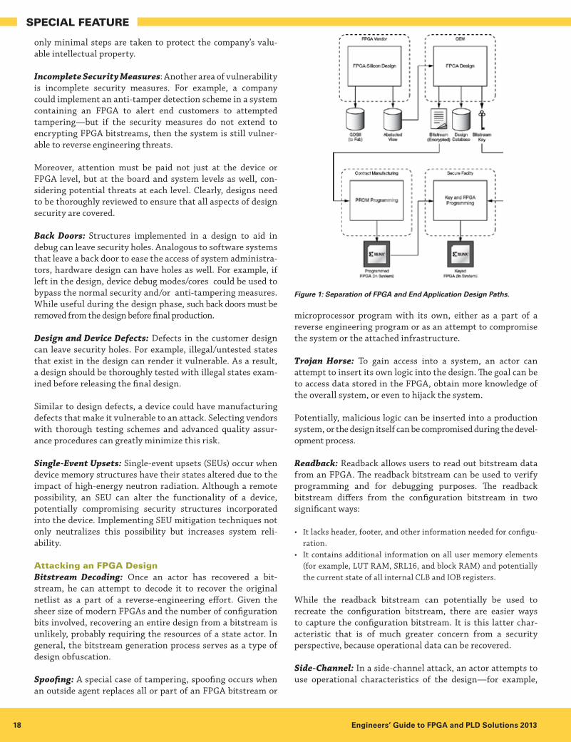
Figure 1: Separation of FPGA and End Application Design Paths.

www.eecatalog.com/fpga 19
Special feature
timing or power—to retrieve keys, learn how to insert faults, or to gain insight into the design.
Fault Insertion: This type of attack attempts to cause a circuit to malfunction in an attempt to force the circuit into a test or debug mode, an invalid state, or to output secret data by introducing glitches (analogous to hitting a vending machine in just the right location to cause it to dispense a can of soda). The actor operates the system outside its normal design or environmental operating conditions by varying clock inputs, randomly forcing inputs, or varying voltage and temperature. With an FPGA, this type of attack can also include modifying bits within the configuration bitstream in an effort to affect functionality.
This type of attack might be successful against a micropro-cessor-based system because a glitch can cause steps in the code to be bypassed. Modern hardware design techniques, however, such as completely defining all states and doing a thorough glitch analysis, make this type of attack against FPGAs difficult to implement.
FPGAs as Secure PlatformsOne of the keys to security is compartmentalization—sepa-rating confidential data between various organizations to prevent any one person or entity from being able to access all the information. By their very nature, FPGAs are a secure platform for design because device manufacture is separated from end-application design by an original equipment manu-facturer (OEM), and end-product manufacture is handled separately. This separation of paths is illustrated in Figure 1.
With an FPGA, therefore, separation of knowl-edge bases is intrinsic to the nature of the device and its method of implementation:
• Thedevice supplierhandles thedesignandmanu-facture of the unprogrammed silicon but does not have access to the end application.• Conversely, the end-application designer does nothave access to the details of how the FPGA base device is designed, nor to its internal security structures. The application design engineer sees only a software-abstracted view of the device.• Productmanufacturingcanbegivenonlyanencrypted bitstream and a bill of material (BOM), and therefore has knowledge neither of the end-applica-tion design nor the FPGA design.• Programmingofthebitstreamdecryptionkeycanbe handled in a secure facility separate from product manufacturing—for example, during final test by the OEM or other trusted third party.
In contrast, with a custom device, the end-application designer and the manufacturer (fab)
have complete details of the device structure and function. Additionally, a custom device can be “de-lidded,” the process of chemically or mechanically removing one layer at a time. Using this method, the entire design database can be recov-ered. Performing the same process on an FPGA might recover the structure of the device, but in the unprogrammed state. No customer data is compromised.
ConclusionTable 1 summarizes the wide range of robust security features offered in Xilinx FPGAs. These features help customers build designs that are not only secure, but resistant to cloning and tampering as well.
These capabilities can be combined in response to various security needs:
• Confidentialityplusanti-cloningprotection:AES• Confidentiality, authentication, plus anti-overbuilding/cloning
protection: AES plus HMAC authentication• Confidentiality, authentication, plus anti-overbuilding/cloning
and anti-spoofing protection: HMAC authentication eFUSE key storage
• Confidentiality, anti-overbuilding/cloning protection, plus longshelf life: AES with eFUSE key storage
• Confidentiality and anti-cloning protection for devices withouteFuse: Device DNA
Working with an FPGA vendor who understands today’s secu-rity threats and has experience in secure design is essential.
XILINX FPGA FAMILY
Virtex-4 Virtex-5 Virtex-6 Spartan-6 7 Series
AES 256-bit encryption (volatile
key battery-backed RAM)
Yes Yes Yes LX75/T,
LX100/T,
LX150/T only
Yes
AES 256-bit encryption
(nonvolatile key - fuses)
No No Yes LX75/T,
LX100/T,
LX150/T only
Yes
Device DNA No No Yes Yes Yes
HMAC bitstream authentication No No Yes No Yes
Hardened readback-disabling
circuitry
Yes Yes Yes Yes Yes
Internal key clear No Yes Yes Yes Yes
Internal configuration memory
clearing (IPROG)
No Yes Yes Yes Yes
On-chip temperature and voltage
monitoring
No Yes Yes No Yes
Table 1: Xilinx FPGA Family Security Features.

20 Engineers’ Guide to FPGA and PLD Solutions 2013
Special feature
References1. FIPS-140-2, Security Requirements for Cryptographic Modules, Federal
Information Processing Standards, U.S. National Institute of Standards and Technology. http://www.nist.gov/itl/upload/fips1402.pdf
2. FIPS-197, Advanced Encryption Standard, Federal Information Processing Standards, U.S. National Institute of Standards and Technology. http://www.nist.gov/itl/upload/fips-197.pdf
3. FIPS-180-3, Secure Hash Signature Standard, Federal Information Pro-cessing Standards, U.S. National Institute of Standards and Technology. http://www.nist.gov/itl/upload/fips180-3_final.pdf
4. FIPS-198-1, Keyed-Hash Message Authentication Code, Federal Informa-tion Processing Standards, U.S. National Institute of Standards and Technology. http://www.nist.gov/itl/upload/FIPS-198-1_final.pdf
Mr. Steven McNeil is a Senior Staff Applications Engineer at Xilinx with 20 years of semiconductor experience spanning a wide range from manufac-turing and circuit design to customer applications. His expertise is in Information Assurance and design security. Mr. McNeil currently manages an Applications team in the Aerospace and Defense Division of Xilinx servicing both the Defense and Commercial markets. Previous to his work in Aerospace and Defense, he held positions in Product Engineering and IC Design working on CPLDs and FPGAs. Prior to Xilinx, he worked at Philips Semiconductor in both Process En-gineering and Device Failure Analysis. Mr. McNeil holds a BS in Electrical Engineering from the University of New Mexico.

www.eecatalog.com/fpga 21
Viewpoint
A couple of weeks after I joined Xilinx in 2008, one of my new colleagues gave me an original copy of the press release announcing our first product, the XC2064, which would eventually come to be known as the world’s first FPGA. The public release date was November 1, 1985 and the announcement came from legendary Silicon Valley public relations firm Regis McKenna. Every once in a while, I’ll pick up the press release and give it another read, because it reminds me how far the FPGA industry has come. The con-trast between what FPGAs were like in 1985 and what they can do today is remarkable—so much so that I think many of them have outgrown the moniker “field-programmable gate array.” Well, at least the “gate array” part.
It’s no easy task naming innovative technologies. Back when Xilinx and Regis McKenna were launching the XC2064, it appears that they hadn’t quite figured out what to call the device. In fact, the headline for the press release reads: “Xilinx Develops New Class of ASIC.” Mean-while, the first paragraph describes the device as follows: “The new device, called a logic cell array, offers a high level of integration together with the versatility of a gate array-like architecture.” The release goes on to describe many truly revolutionary features, including “unlimited reprogramming without removal from the system,” “64 configurable logic blocks and 58 I/O blocks…[and] 1,000 to 1,500 gate equivalents.” These were all quite impressive for the time. Clearly, Xilinx had set its sights on displacing PALs and “bipolar and CMOS programmable products, LS TTL [low-power Schottky transistor-transistor logic] com-ponents and gate arrays.” Who knew at the time that this new class of device would one day compete with ASICs and consolidate the functions of many chips into one?
I started covering the EE design space in 1995, and so I missed the point in time when these “logic cell array ASICs” became commonly known as field-programmable gate arrays (FPGAs). What’s a bit puzzling to me is how “gate array” got into the name? In 1985, the public relations team likely called the devices “a new class of ASIC” because even back then, ASICs were starting to rapidly displace gate arrays. By the time I began writing about electronic design, gate arrays were gone, daddy, gone. I get the field-program-mable part. That’s an engineering-esque way of saying that the device was reprogrammable. But “gate arrays”? Really?
Certainly, the devices we offer today are so much more than gate arrays that are “reprogrammable”. Back in 2008 we began executing on a plan that redefines the possibilities
of programmability. At the 28-nanometer mode, we deliv-ered three lines of All Programmable FPGAs (the Virtex-7, Kintex-7 and Artix-7 devices), but didn’t stop there. In its 28-nm generation, we also delivered the first homogeneous and heterogeneous All Programmable 3D ICs, which shatter capacity and bandwidth records, respectively.
What’s more, Xilinx is delivering to customers today the Zynq-7000 All Programmable SoC, which marries an ARM dual-core Cortex-A9 MPCore, programmable logic and key peripherals all on a single device. On top of these silicon innovations, we launched a fresh, state-of-the-art design suite called Vivado to help customers leverage the new device families to achieve new levels of system integration, reduce BOM costs, lower power consumption and speed system per-formance. Not only do the latest offerings have innovative programmable logic, they also boast programmable I/O, DSP slices and embedded processors, making them also software programmable—they are truly All Programmable, enabling truly reprogrammable systems, not just reprogrammable logic. They certainly are not gate arrays!
Mike Santarini is the publisher of Xilinx’s Xcell Journal. Prior to joining Xilinx, Santarini was a senior editor at EDN magazine, EE Times and In-tegrated System Design magazine. He holds BA in English from Santa Clara, University (1995).
So Much More Than Gate ArraysBy Mike Santarini, Senior Manager Xcell Journal and Editorial Services

22 Engineers’ Guide to FPGA and PLD Solutions 2013
Advertorial
With the large-scale integration of today’s systems-on-chips (SoCs), FPGAs can help embedded designers reduce cost, weight, area and power; they also offer flexibility so that designers can respond to new standards, evolving customer needs and other requirement changes and still meet their time-to-market window. But the complex architectures of these devices can also present new challenges to board-level designers.
Whether you’ve implemented your custom design in a develop-ment board and need assistance, lack resources to create the board-level design or are considering designing your own solu-tion, our years of experience in FPGA board-level design are here to assist you. Through development of numerous COTS and custom FPGA board designs we’ve identified a number of steps and considerations that are essential to a successful design cycle; steps that will help you to avoid a costly re-spin and delay your time to market.
Review peripheral interfaces that will be connected to the FPGAFirst we review the customer’s high-level design to determine the peripheral interfaces connected to the FPGA. Then we analyze each of these interconnects and determine their speed, interface, voltage level, I/Ostandards and how many pins are required. Second, we review the customer intended FPGA application, with the goal of estimating the design metrics. This leads to an indication of the logic density and speed grade needed from the FPGA. By analyzing the FPGA design itself, we can answer some critical questions. What are the internal clock rates? How many logic resources are required? Is any special hard IP required, such as DSP slices, Ethernet MACs or PCIe endpoints?Answering these questions early in the design phase will ensure that your initial FPGA selection will meet the needs of the design out of the gate.
Power, Create a power budget, Review SequencingFrom the early stages of the design, we create a power budget that defines the current required per FPGA voltage rail. This budgetis based on resource estimates including logic usage, block memory usage, internal clock rates, I/O quantity, I/O data rates and I/O voltage levels. It’s important to be aware of any voltage rail sequencing requirements for the FPGA and the sequencing requirements for the surrounding peripherals that might conflict with the FPGA. In addition, we need to be aware of anysequencing requirements for the design –are there certain ICs that need to be powered up before the FPGA or vice-versa or if there is no method to disable or idle a specific IC, is it necessary to delay its power-up until the FPGA is configured and ready?We also need to deter-mine how this will fit with on-board power supplies that might
be present, which will also helpdefine what additional supplies or power monitoring circuitry will be required on the PCB design.
Additionally, it’s important to know whether there are voltage rails that need to be especially quiet. For example, perhaps the FPGA core voltage is 1.2V and the SERDES supply is also 1.2V; it might be necessary to isolate and drive the SERDES supply sepa-rate from the noisy core voltage. And we always want to consider the possibility of future FPGA capacity upgrades, and whether the extra power requirement has been factored in.
Configuration ConsiderationsConfiguring a FPGA can be a trivial task, or it can be very com-plicated, depending on the application. Every design should have at a minimum a JTAG connection for debugging, development and production testing, as well as persistent storage for the appli-cation. The persistent storage is usually in the form of serial or parallel flash or a hybrid device produced by the FPGA vendor. In more complex designs, the FPGA could be configured by micro-controller, CPU, CPLD or other FPGA. But focusing on the flash design, there are quite a few things to consider. Are the flash con-figuration pins on the FPGA dual-purpose? Are these pins already tasked and connected to another device? If so, we need to make sure the I/O standards are compatible – flash is typically 3.3V CMOS. If the signals are shared, we need to know if the peripheral interface is high-speed; if so, it may not tolerate having another device in the signal path.
Sequencing requirements, such as the flash needing to be pow-ered up a certain amount of time before it can be accessed by the FPGA also needs to be considered, as well as timing requirements, such as whether the FPGA can read data from the flash and con-figure itself in time. A perfect example is PCI and PCI Express, which specify that a device must be ready approximately 100 ms after power-on.
Programming on the Fly:Many products need to be field-upgradeable over Ethernet,PCIe or USB, in order to add new features or fix bugs. In any of those cases, the designer has to consider whether the flash is writeable over the general I/O. Some FPGA vendor-specific flash is read only, and can only be written to via JTAG. Plus,there are a number of other possible issues, including whether the FPGA can restart the configuration cycle on the fly (a soft boot) without doing a power cycle (complete on/off), and whether the other circuitry can handle a temporary interruption in the state of the FPGA as it goes from configured to an un-configured state. We also think about what happens if the flash programming operation is inter-
Tips, Tricks and Hardware Design Services for FPGA DevelopersBy Michele Kasza, Vice President Sales, Connect Tech Inc.

www.eecatalog.com/fpga 23
Advertorial
ContaCt InformatIon
Connect Tech Inc.42 Arrow RoadGuelph, OntarioCanada N1K 1S6Telephone: 519-836-1291Fax: [email protected]://www.connecttech.com
rupted; for example, if the Ethernet cable is disconnected. What if the flash is corrupt? In this case, consider designing a failsafe configuration scheme where the first half of the flash contains a known good golden image and the second half contains the actual application image.
Recommended Pre-Production steps:After all the FPGA pins have been allocated and the board sche-matic design is nearing completion, it is very good practice to run the FPGA design through the vendor synthesis and placement tool suite before beginning the PCB layout. Usually the FPGA RTL design is nowhere near completion; however, it is good to generate at least a useable framework of the RTL design, which at minimum allocates the proper I/O resources. Developers typi-cally make every effort to properly map each I/O peripheral to a specific bank and assign any clocking signals to the appropriate pins, but there are often device limitations that are only apparent if you’ve had the time to read all 300 pages of all ten user guides. Simply running this FPGA framework through the FPGA tool suite can help uncover these limitations with the DRC. Most of the limitations can be seen in lower-cost devices; for example, some pins are setup for inputs only, or in the specific case of the Xilinx Spartan-6 FPGA, only banks 0 and 2 can accommodate LVDS outputs, while every bank can handle LVDS inputs. Once the board goes to the layout stage, hardware engineering might decide that the routing will be much easier if DDR3 data pin 1 is swapped with data pin 15, for instance. It’s always good practice to run this change through the tool suite to see if it passes all checks.
Choosing your FPGAOften our customers are predisposed to one FPGA vendor or another, typically based on past experience or reputation. What-ever the case, there are many factors to analyze with respect to cost. Those include the number of I/O, size of logic resources, maximum internal clock rate, maximum general I/O clock rate, availability and quantity of SERDES pins, size of the package and configuration options. The analysis of the I/O peripheral and logic design that we perform up front, which were described previously, should help narrow the choice. However, there are several other, less-obvious factors to consider before selecting the device. For instance, the data rates and clock rates quoted in the marketing material are often based on the highest speed grade available and these devices often come at a premium. Another thing to look at is how I/O resources are grouped and mapped onto the FPGA pins. For example, a device might have 240 I/O that might be in three banks of 80 pins or six banks of 40 pins. If your design has multiple I/O standards – such as 1.5V for DDR3, 1.8V HSTL for Ethernet, 2.5V LVDS for ADC/DAC and 3.3V for CMOS – the number of banks will be important.
We typically make the FPGA vendor decision based on a few main factors. The technologies they offer are important of course, but we also consider the support given by that vendor’s FAEs and online resources. Design software is another big component – each vendor will use a different set of tools, so use what you are most comfortable with or what has the best features for your needs.
Future Proof your FPGA selectionIt’s very important to consider your upgrade path – this is often overlooked in the early stages of the design but can turn out to be a real advantage if leveraged properly for your product. Some FPGA devices will have a pin compatible upgrade path to a larger capacity parts within the same FPGA family. This means that you can select a smaller device for your basic product that provides the end-customer a low cost, reduced feature set option; while keeping the same board design for the high cost, full featured product. Or if the RTL design simply outgrows the selected part in terms of logic capacity, you want to make sure there’s a high-density part available in the same footprint.
Looking for a design partner?Although a manufacturer of many COTS products, custom design is part of our day-to-day operation. Our design process has been refined over many years resulting in successfully completed, on-time and on-budget projects time and time again.
Improved time to market:Our COTS product lines act as an IP pool from which we draw fromwith every custom design. With expertise over a wide variety of bus architectures and I/O interfaces, the learning curve forcustom designs is always minimal. This signature-method equals improved time to market and ensures a very high potential for a successful Revision A build. On average, our time to market on functional prototypes from time of engagement to time of delivery is approximately an 8 week window depending on project complexity.
Manufacturing Expertise:Beyond board-level design we create prototype qualification-plansfor each unique product, ensuring all custom product is fully verified using appropriatecompliancetools, such as PCI_SIG software and test equipment. Power supplies and batteries are fully stressed and wide range temperature testing is part of the deliverables offered by Connect Tech design services.
Beyond the prototype phase we can quickly ramp up to produc-tion quantities under strict ISO 9001:2008 procedures, handle lifecycle management at the component level and finish with packaging and delivery of 100% verified hardware.
Looking for a design partner with robust industry experience and impressive time to market?
Contact us today to find out how we can help.

New stacked silicon architecture from Xilinx makes your big design much easier to prototype.Partitioning woes are forgotten, and designs run at near final chip speed. The DINI Group DNV7F1board puts this new technology in your hands with a board that gets you to market easier, faster andmore confident of your design’s functionality running at high speed. DINI Group engineers put thefeatures you need most, right on the board:
• 10GbE
• USB 2
• PCIe, Gen 1, 2, and 3
• 240 pin UDIMM for DDR3
There is a Marvel Processor for any custom interfaces you might need andplenty of power and cooling for high speed logic emulation. Software andfirmware developers will appreciate the productivity gains that come with thislow cost, stand-alone development platform.
Prototyping just got a lot easier, call DINI today and get your chip up to speed.
www.dinigroup.com • 7469 Draper Avenue • La Jolla, CA 92037 • (858) 454-3419 • e-mail: [email protected]

212x276_USA_FPGA_M2.indd 1 23.10.12 07:56
C
M
Y
CM
MY
CY
CMY
K
D-GSMMWC121087 CLFBPM 8.125x10.875-99.ai 1 12年10月12日 下午12:50

Portfolio: All Programmable FPGAs, SoCs, and 3D ICs available today
Product: An extra node of performance, power and integration
Productivity: Unmatched time to integration and implementation
www.xilinx.com
All Programmable SoC All Programmable 3D IC Next Gen Design Environment
A Generation Ahead
CS1223_CES_Print_Ad_FINAL_rev.indd 1 10/31/2012 10:45:01 AM

www.eecatalog.com/fpga Boards&Kits•29
ContaCt InformatIon
Xilinx, Inc.
Xilinx, Inc.2100 Logic DriveSan Jose, CA 95124USA720-480-2698 [email protected]
AvAILABILITY
For the latest information on the Zynq-7000 SoC ZC702 Evaluation Kits visit: www.xilinx.com/ZC702
APPLICATION AREAS
Aerospace/Defense, Automotive, Industrial Automation, Medical Imaging
Zynq-7000 SoC ZC702 Evaluation Kit Supported FPGA/CPLDs: Zynq-7000 All Programmable SoCs
The Xilinx® ZYNQ™-7000 SoC ZC702 Evaluation Kit gives developers a complete development platform for prototyping, evaluating and developing Zynq-7000 All Programmable SoC designs. The included targeted reference design jump-starts develop-ment, and enables in-depth exercising of the ARM processing system and Xilinx 28nm programmable logic architecture. Additional reference designs and industry-standard FPGA Mezzanine Connectors (FMCs) let developers scale and customize designs using Xilinx and third-party daughter cards to best fit their application and system with this development board. This evaluation kit offers a wide feature set and abundant I/O expandability, to shorten time to market for applications that call for industry-leading performance, feature differentiation, and power effi-ciency.
FEATuRES & BENEFITS
◆ Productivity-boosting kit, including silicon, devel-opment tools, IP, and reference designs
◆ Wide feature set, with abundant I/O expandability, to develop solutions for most markets
◆ Foundation for Zynq-7000 SoC - based designs
◆ Best-in-class tools, operating system support, and ecosystem (including ARM community)
TECHNICAL SPECS
◆ ZC702 Evaluation Board featuring the XC7Z020-1CLG484CES device and Analog Mixed Signal evaluation card
◆ Full seat ISE® Design Suite Embedded Edition – device locked
◆ Step-by-Step Getting Started Guide, Hardware User Guide, and Reference Design/Design Exam-ple User Guide
◆ Schematics and PCB files, Demonstrations, and Board design files
◆ Cables and power supply
Design KitsD
esig
n Ki
ts
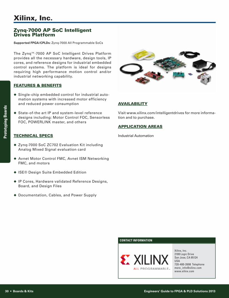
30•Boards&Kits Engineers’ Guide to FPGA & PLD Solutions 2013
ContaCt InformatIon
Xilinx, Inc.
Xilinx, Inc.2100 Logic DriveSan Jose, CA 95124USA720-480-2698 [email protected]
AvAILABILITY
Visit www.xilinx.com/intelligentdrives for more informa-tion and to purchase.
APPLICATION AREAS
Industrial Automation
Zynq-7000 AP SoC Intelligent Drives Platform Supported FPGA/CPLDs: Zynq-7000 All Programmable SoCs
The Zynq™-7000 AP SoC Intelligent Drives Platform provides all the necessary hardware, design tools, IP cores, and reference designs for industrial embedded control systems. The platform is ideal for designs requiring high performance motion control and/or industrial networking capability.
FEATuRES & BENEFITS
◆ Single-chip embedded control for industrial auto-mation systems with increased motor efficiency and reduced power consumption
◆ State-of-the art IP and system-level reference designs including: Motor Control FOC, Sensorless FOC, POWERLINK master, and others
TECHNICAL SPECS
◆ Zynq-7000 SoC ZC702 Evaluation Kit including Analog Mixed Signal evaluation card
◆ Avnet Motor Control FMC, Avnet ISM Networking FMC, and motors
◆ ISE® Design Suite Embedded Edition
◆ IP Cores, Hardware validated Reference Designs, Board, and Design Files
◆ Documentation, Cables, and Power Supply
Prototyping Boards Pr
otot
ypin
g B
oard
s

www.eecatalog.com/fpga Boards&Kits•31
ContaCt InformatIon
Xilinx, Inc.
Xilinx, Inc.2100 Logic DriveSan Jose, CA 95124USA(408) 559-7778 Telephonewww.xilinx.com
AvAILABILITY
Visit www.xilinx.com/ams101 for more information and to purchase.
APPLICATION AREAS
Industrial, Scientific, Medical
Xilinx AMS101 Evaluation Card Supported FPGA: 28nm based-products
The AMS101 Evaluation Card is part of the Analog Mixed Signal Evaluation (AMS) Platform which allows testing of the Xilinx Analog-to-Digital Converter (XADC). This daughter card can be paired with any Xilinx 7 series or Zynq™-7000 All Programmable SoC baseboard (including the Avnet® ZedBoard). 7 series FPGAs each feature two 1 Mega-sample per second (Msps) Xilinx ADCs built into the FPGA or Zynq-7000 SoC. The AMS technology combines the XADC analog measurement with the FPGA logic for simple system monitoring to more signal processing-intensive tasks like linearization, calibration, oversampling, and fil-tering.
Reference and demo designs are available at www.xilinx.com/ams to validate the XADC’s performance, including the internal temperature and supply voltage sensors, signal-to-noise ratio, effective number of bits, linearity, and many other specifications. The AMS101 Evaluation Card includes an on-board 16-bit DAC which provides an analog test source to the XADC. Paired with the AMS Evaluator tool and AMS reference designs, the DAC can supply a precision sine wave or DC signal. The AMS101 Evaluation Card also includes BNC connectors for applying a single differential external signal to the card’s gold posts.
FEATuRES & BENEFITS
◆ AMS101 Evaluation Card plugs into the XADC header available on any of the 7 series or Zynq-7000 SoC baseboard
◆ AMS101 Evaluation Card pairs with free AMS Evaluator tool for analyzing analog data, internal temperature and voltage measurements, and saving data to a .csv file
◆ BNC connector included for external signal source connection
◆ Evaluates XADC 12-bit, 17-channel, 1Msps dual ADCs
◆ On-board 16-bit dual DAC for analog test signals or external signals supported
◆ Reference designs supported: AC701, ZC702, KC705, VC707; Demo designs supported: ZC706, Avnet ZedBoard
fPGa
Boards fP
Ga
Boa
rds

32•Boards&Kits Engineers’ Guide to FPGA & PLD Solutions 2013
ContaCt InformatIon
Xilinx, Inc.
Xilinx, Inc.2100 Logic DriveSan Jose, CA 95124USA408-559-7778 [email protected]/kits
◆ Complete with universal power supply, accessory cables, and downloadable documentation with schemat-ics, Gerber files, board BOM, and detailed user guides
TECHNICAL SPECS
◆ Xilinx SP601 Evaluation Kit for low-cost Spartan-6 FPGA evaluation and the Xilinx SP605 Evaluation Kit for low-cost connectivity applications
◆ Avnet LX16 Evaluation Kit for low-power, battery-power applications such as handheld data gathering, human machine interface, and embedded control
◆ Avnet LX150T Development Kit for PCI Express® bridges, Ethernet/Internet and video applications, and embedded controllers
◆ All kits feature industry-standard FPGA Mezzanine Card (FMC) connector enabling scaling and customization of base boards for specific application and market needs
AvAILABILITY
Available Today! Visit www.xilinx.com/kits
APPLICATION AREAS
Aerospace/Defense, Automotive, Broadcast, Consumer, Data Processing and Storage, Industrial Automation, Medical Imaging, Wired Communcations, Wireless Communications
Spartan-6 FPGA Evaluation and Development KitsSupported FPGA/CPLDs: Spartan-6 FPGA
Xilinx and Avnet provide a comprehensive offering of Spartan®-6 FPGA evaluation and development kits that enable designers to achieve an optimum balance of cost, power and performance.
The SP601 Evaluation Kit is a low-cost, entry-level envi-ronment for evaluating the Spartan-6 FPGA family with system design capabilities that include DDR2 memory control, flash, Ethernet, general-purpose I/O, and UART to name a few. The SP605 Evaluation Kit is a highly scal-able base platform for developing low-cost applications requiring connectivity with high-speed serial trans-ceivers, DDR3 memory control, DVI, parallel linear flash, and Tri-mode Ethernet.
The Xilinx Spartan-6 LX16 Evaluation Kit, featuring Texas Instruments battery management devices and power regulation circuitry and the Cypress PSoC® 3 Programmable System on Chip with embedded 8051 for an ultra-low-power controller. Avnet also offers the full-featured Xilinx Spartan-6 LX150T Development Kit for designing and verifying applications based on the Spartan-6 LXT FPGA family.
The low-cost Spartan®-6 FPGA LX9 MicroBoard is the perfect solution for designers interested in exploring the MicroBlaze™ soft processor or Spartan-6 FPGAs in general. The kit comes with several pre-built MicroBlaze “systems” allowing users to start software develop-ment just like any standard off-the-shelf microprocessor. The included Software Development Kit (SDK) provides a familiar Eclipse-based environment for writing and debugging code.
FEATuRES & BENEFITS
◆ Xilinx SP601 and Avnet LX16 Evaluation Kits feature base board with Spartan-6 LX16 FPGA and ISE® Web-PACK™ Design Suite (supporting Windows and Linux)
◆ Xilinx SP605 Evaluation Kit features base board with Spartan-6 LX45T FPGA and ISE Design Suite Logic Edition (device-locked)
◆ Avnet LX150T Development Kit features base board with Spartan-6 LX150T FPGA and ISE Design Suite Logic Edition (device-locked)
◆ The Spartan-6 LX-9 MicroBoard kit includes peripherals and expansion interfaces making it the kit ideal for a wide variety of applications. From a system running an RTOS to a Linux-based web server, the Spartan-6 LX9 MicroBoard can help you validate your next design idea.
fPGa
BoardsfP
Ga
Boa
rds
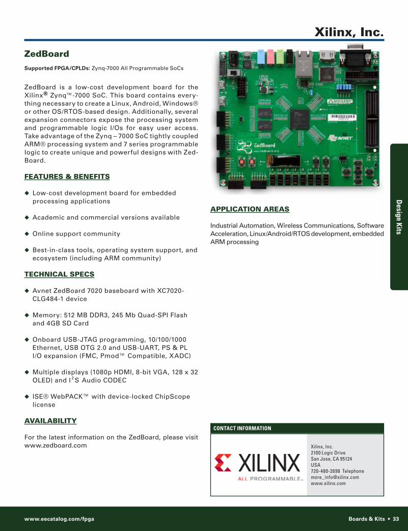
www.eecatalog.com/fpga Boards&Kits•33
ContaCt InformatIon
Xilinx, Inc.
Xilinx, Inc.2100 Logic DriveSan Jose, CA 95124USA720-480-2698 [email protected]
APPLICATION AREAS
Industrial Automation, Wireless Communications, Software Acceleration, Linux/Android/RTOS development, embedded ARM processing
ZedBoard Supported FPGA/CPLDs: Zynq-7000 All Programmable SoCs
ZedBoard is a low-cost development board for the Xilinx® Zynq™-7000 SoC. This board contains every-thing necessary to create a Linux, Android, Windows® or other OS/RTOS-based design. Additionally, several expansion connectors expose the processing system and programmable logic I/Os for easy user access. Take advantage of the Zynq – 7000 SoC tightly coupled ARM® processing system and 7 series programmable logic to create unique and powerful designs with Zed-Board.
FEATuRES & BENEFITS
◆ Low-cost development board for embedded processing applications
◆ Academic and commercial versions available
◆ Online support community
◆ Best-in-class tools, operating system support, and ecosystem (including ARM community)
TECHNICAL SPECS
◆ Avnet ZedBoard 7020 baseboard with XC7020-CLG484-1 device
◆ Memory: 512 MB DDR3, 245 Mb Quad-SPI Flash and 4GB SD Card
◆ Onboard USB-JTAG programming, 10/100/1000 Ethernet, USB OTG 2.0 and USB-UART, PS & PL I/O expansion (FMC, Pmod™ Compatible, XADC)
◆ Multiple displays (1080p HDMI, 8-bit VGA, 128 x 32 OLED) and I 2 S Audio CODEC
◆ ISE® WebPACK™ with device-locked ChipScope license
AvAILABILITY
For the latest information on the ZedBoard, please visit www.zedboard.com
Design KitsD
esig
n Ki
ts

34•Boards&Kits Engineers’ Guide to FPGA & PLD Solutions 2013
ContaCt InformatIon
Xilinx, Inc.
TECHNICAL SPECS
◆ VC707 Base Board with Vintex-7 XC7VX485T-2FFG1761 FPGA
◆ Full seat of Vivado™ Design Suite: Design Edition. Device-locked to the Virtex-7 XC7VX485T FPGA
◆ Reference designs and demonstrations (please see Xilinx.com for latest designs) and board design files
◆ Documentation including a step-by-step Getting Started Guide
◆ USB Cables, Ethernet Cable, and universal power supply
AvAILABILITY
For more information about the Virtex-7 FPGA VC707 Evaluation Kit please visit www.xilinx.com/vc707
APPLICATION AREAS
Wired, Wireless, Aerospace and Defense, Medical, Broad-casting
vIRTEX-7 FPGA vC707 EvALuATION KITSupported FPGA/CPLDs: Virtex-7 FPGA
The Xilinx Virtex®-7 VC707 FPGA Evaluation Kit pro-vides a highly flexible base platform with an out of the box launch pad to evaluate and leverage designs that deliver breakthrough performance, capacity and power efficiency.
As a Base Level Targeted Design Platform, this kit provides a flexible environment for designs that need to implement a DDR3 memory interface, 10Gigabit Ethernet, PCI Express®, Analog Mixed Signal (AMS) capabilities, and other high-speed serial connectivity. Based on the Virtex-7 VX485T-2 FPGA, the kit is the optimal choice for advanced systems that need the highest performance and highest bandwidth con-nectivity, including advanced systems for wired and wireless communications, Aerospace and Defense, medical, and broadcasting markets.
The highly flexible kit combines fully integrated hard-ware, software and IP with pre-verified reference designs that maximize productivity and let designers immedi-ately focus on their unique project requirements.
FEATuRES & BENEFITS
◆ Virtex-7 FPGA family and 28nm leadership offer-ing new benchmarks for performance and 50% power savings
◆ Faster start-up with integrated silicon, software, IP and complete documentation
◆ Rapid evaluations with Base Reference Designs and other pre-verified examples that exercise device and board features
◆ Convenient, easy-to-use GUI displays combine results from different implementations
fPGa
BoardsfP
Ga
Boa
rds
Xilinx, Inc.2100 Logic DriveSan Jose, CA 95124USA720-480-2698 Telephonewww.xilinx.com

www.eecatalog.com/fpga Boards&Kits•35
ContaCt InformatIon
Xilinx, Inc.
Xilinx, Inc.2100 Logic DriveSan Jose, CA 95124USA720-480-2698 Telephonewww.xilinx.com
AvAILABILITY
For more information about the Artix-7 FPGA AC701 Evaluation Kit please visit www.xilinx.com/ac701
APPLICATION AREAS
Industrial Automation, Wireless Communications, Software Acceleration, Linux/Android/RTOS development, embedded ARM processing
Artix-7 FPGA AC701 Evaluation Kit Supported FPGA/CPLDs: Artix-7 FPGA
The Artix™-7 FPGA AC701 Evaluation Kit features the leading system performance per watt Artix-7 family to get you quickly prototyping for your cost sensitive applications. This includes all the basic components of hardware, design tools, IP, and pre-verified refer-ence designs. This also features a targeted reference design enabling high-performance serial connectivity and advanced memory interfacing equipped with a full license for the Northwest Logic DMA engine.
FEATuRES & BENEFITS
◆ Increased system performance featuring the Artix-7 XC7A200T FPGA: up to sixteen 6.6G GTs, 930 GMAC/s, 13Mb BRAM, 1.2Gb/s LVDS, and DDR3-1066
◆ Enabling programmable system integration: Up to 215K logic cells; AMS integration, and AXI IP
◆ Small packaging and lower BOM costs
◆ 65% lower static and 50% lower power than previ-ous generation devices
◆ Scalable, optimized architecture, comprehensive design tools, and IP for design productivity
TECHNICAL SPECS
◆ AC701 evaluation board featuring the XC7A200T-2FBG676CES FPGA
◆ Targeted Reference Design featuring DDR3, PCIe® and DMA Including a full license for the Northwest Logic DMA
◆ AMS 101 evaluation card
◆ Full seat Vivado™ Design Suite: Design Edition Device-locked to the Artix-7 XC7A200T FPGA
◆ Documentation including a step-by-step Getting Started Guide
Design KitsD
esig
n Ki
ts

36•Boards&Kits Engineers’ Guide to FPGA & PLD Solutions 2013
ContaCt InformatIon
PENTEK
Pentek One Park WayUpper Saddle River, NJ 07458USA201-818-5900 Telephone201-818-5904 [email protected]
◆ LVPECL clock/sync bus for multimodule synchronization◆ PCI Express (Gen. 1, 2 & 3) interface up to x8
AvAILABILITY
Contact Pentek for price and availability.
APPLICATION AREAS
Aerospace/Defense, Data Processing and Storage, Medical Imaging, Wired Communcations, Wireless Communications.
Model 71720 3-Channel 200 MHz A/D and 2-Channel 800 MHz D/A with virtex-7 FPGA - XMC Module
The Onyx Model 71720 3-channel, 200 MHz A/D, 2-channel 800 MHz D/A module is based on the high density Xilinx Virtex-7 FPGA. Pentek is among the first board suppliers to leverage the high-performance, low-power Virtex-7 FPGA family, addressing the most challenging unmanned aerial vehicle (UAV), radar and communications applications.
GateXpress is a sophisticated FPGA-PCIe hardware engine for managing the reconfiguration of the FPGA, representing a major enhancement in the Onyx architecture. At power up, the GateXpress manager immediately presents a PCIe target to the host com-puter for discovery and enumeration, giving the FPGA time to load from FLASH. This is especially important for larger FPGAs where the loading time can exceed the PCIe discovery window, typically 100 ms on most PCs.
The 71720 architecture supports four independent DDR3 SDRAM memory banks. Each bank is 1 GB deep and is an integral part of the module’s DMA capa-bilities, providing FIFO memory space for creating DMA packets. Built-in memory functions include an A/D data transient capture mode and D/A waveform playback mode. In addition to the factory-installed functions, custom user-installed IP within the FPGA can take advantage of the memories for many other purposes.
For applications that require specialized functions, users can install their own custom IP for data pro-cessing using the GateFlow FPGA Design Kit.
FEATuRES & BENEFITS
◆ Complete radar and software radio interface solution◆ Supports Xilinx Virtex-7 VXT FPGAs◆ GateXpress supports dynamic FPGA reconfigura-
tion across PCIe◆ Three 200 MHz 16-bit A/Ds◆ One digital upconverter
TECHNICAL SPECS
◆ Two 800 MHz 16-bit D/As◆ 4 GB of DDR3 SDRAM◆ Sample clock synchronization to an external
system reference
fPG
a B
oardsfP
Ga
Boa
rds

www.eecatalog.com/fpga DevelopmentTools•37
ContaCt InformatIon
Xilinx Inc.
Xilinx, Inc.2100 Logic DriveSan Jose, CA 95124USA408-559-7778 Telephone
TECHNICAL SPECS
◆ Vivado Design Suite: WebPACK Edition - The No cost, device-limited version of the Vivado Design Suite: Design Edition
◆ Vivado Design Suite: Design Edition Simplified design integration and implementation. The Design Edition enables new levels of flexibility for designing, integrating, implementing and reusing modules.
◆ Vivado Design Suite: System Edition – The same front-to-back support as Design Edition plus Vivado High-Level Synthesis and System Generator for DSP
AvAILABILITY
Available Today!
Download today www.xilinx.com/download
vivado Design SuiteSupported FPGA/CPLDs: Xilinx All Programmable FPGAs, SoCs and 3D ICs
Programmable devices are at the heart of most sys-tems today, enabling not only programmable logic design, but programmable systems integration. Xilinx has transformed from an FPGA company to an ‘All Programmable’ company, offering technology from logic and IO to SW programmable ARM® processing systems and beyond.
With the next decade of programmable platforms, comes the next generation design environment that meets the aggressive pace and the need for enhanced productivity. Xilinx introduces the Vivado™ Design Suite, an IP and system-centric design environment built from the ground up to accelerate productivity for the next generation of ‘All Programmable’ devices. The new Vivado Design Suite is already proven to accelerate integration and implementation by 4x over traditional design flows, reducing cost by simpli-fying design and automating, not dictating, a flexible design environment.
Vivado Design Suite provides a highly integrated design environment with acompletely new generation of system-to-IC level tools, all built on the backbone of a shared scalable data model and a common debug environment. It is also an open environment based on industry standards such as AMBA® AXI4 inter-connect, IP-XACT IP packaging metadata, the Tool Command Language (Tcl), Synopsys® Design Con-straints (SDC) and others that facilitates customized design flows.
Vivado was architected to enable the combination of all types of programmable technologies and scale up to 100M ASIC equivalent gate designs.
FEATuRES & BENEFITS
◆ Next generation of system-to-IC level tools, built on the backbone of a shared scalable data model and a common debug environment
◆ 4x productivity advantage drives beyond program-mable logic to programmable systems integration
◆ All Programmable’ device support including 3D stacked silicon interconnect technology, ARM pro-cessing systems and Analog Mixed Signal (AMS)
Design toolsD
esig
n to
ols
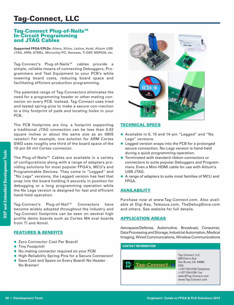
38•DevelopmentTools Engineers’ Guide to FPGA & PLD Solutions 2013
ContaCt InformatIon
Tag-Connect, LLC
Tag-Connect, LLC469 Cherry Ave San Bruno, CA 94066 USA+1 877 244 4156 Telephone+1 877 244 4156 [email protected]
TECHNICAL SPECS
◆ Available in 6, 10 and 14-pin “Legged” and “No Legs” versions.
◆ Legged version snaps into the PCB for a prolonged secure connection. No-Legs version is hand-held during a quick programming operation.
◆ Terminated with standard ribbon connectors or connectors to suite popular Debuggers and Program-mers. Even a Mini-HDMI cable for use with Altium’s USB JTAG.
◆ A range of adapters to suite most families of MCU and FPGA.
AvAILABILITY
Purchase now at www.Tag-Connect.com. Also avail-able at Digi-Key, Telexsus.com, TheDebugStore.com and others. See website for full details.
APPLICATION AREAS
Aerospace/Defense, Automotive, Broadcast, Consumer, Data Processing and Storage, Industrial Automation, Medical Imaging, Wired Communcations, Wireless Communications
Tag-Connect Plug-of-Nails™ In-Circuit Programming and JTAG Cables Supported FPGA/CPLDs: Altera, Xilinx, Lattice, Actel, Altium USB JTAG, ARM, ATMEL, Microchip PIC, Renesas, TI DSP, MSP430, etc.
Tag-Connect’s Plug-of-Nails™ cables provide a simple, reliable means of connecting Debuggers, Pro-grammers and Test Equipment to your PCB’s while lowering board costs, reducing board space and facilitating efficient production programming.
The patented range of Tag-Connectors eliminates the need for a programming header or other mating con-nector on every PCB. Instead, Tag-Connect uses tried and tested spring-pins to make a secure con¬nection to a tiny footprint of pads and locating holes in your PCB.
The PCB footprints are tiny, a footprint supporting a traditional JTAG connection can be less than 0.02 square inches or about the same size as an 0805 resistor! For example, one solution for ARM Cortex SWD uses roughly one third of the board space of the 10-pin 50 mil Cortex connector.
The Plug-of-Nails™ Cables are available in a variety of configurations along with a range of adapters pro-viding solutions for most popular FPGA’s, MCU’s and Programmable Devices. They come in “Legged” and “No Legs” versions, the Legged version has feet that snap into the board holding it securely in position for debugging or a long programming operation while the No Legs version is designed for fast and efficient hand-held operation.
Tag-Connect’s Plug-of-Nail™ Connectors have become widely adopted throughout the industry and Tag-Connect footprints can be seen on several high profile demo boards such as Cortex M4 eval boards from TI and Atmel.
FEATuRES & BENEFITS
◆ Zero Connector Cost Per Board! ◆ Tiny Footprint! ◆ No mating connector required on your PCB!◆ High-Reliability Spring-Pins for a Secure Connecion! ◆ Save Cost and Space on Every Board! No Header -
No Brainer!
DSP and Em
bedded Developm
ent tools DSP
and
Em
bedd
ed D
evel
opm
ent t
ools

www.eecatalog.com/fpga FPGAs&CPLDs•39
ContaCt InformatIon
Xilinx, Inc.
Xilinx, Inc.2100 Logic DriveSan Jose, CA 95124USA408-559-7778 Telephonewww.xilinx.com/artix7
TECHNICAL SPECS
◆ 740 DSP Slices enabling 930 GMACs of performance
◆ Up to 16 High Speed serial transceivers supporting line rates up to 6.6 Gbps
◆ 3.3V capable I/O to enable interfacing to legacy components
◆ Low Cost wire-bound packaging
◆ Chip-scale packages for smallest form factor
AvAILABILITY
Visit www.xilinx.com/artix7 to learn more
APPLICATION AREAS
Automotive, Consumer, Industrial Automation, Medical Imaging, Wired Communcations, Wireless Communica-tions
Artix-7 FPGAsSupported FPGA/CPLDs: 28nm based-product
The Xilinx Artix™-7 FPGA family establishes a new standard for lowest cost and lowest power. Leveraging a common 28nm architecture, Artix-7 delivers over two times the capacity, 30% higher performance, 50% lower power consumption as compared to existing tech-nologies – and is designed to address the demands of high-volume markets.
Artix-7 FPGAs provides higher integration and intro-duces Agile Mixed Signal capability for the first time in a low-cost FPGA, enabling customization for end user applications. Whether complex analog signal condi-tioning or simple analog monitoring, the Agile Mixed Signal technology will enable lower system cost, higher system reliability and customization beyond off the shelf analog components.
FEATuRES & BENEFITS
◆ Built on a common 28nm architecture designed for maximum power efficiency
◆ Logic up to 215K logic cell density at lower price points
◆ A new standard for best cost for higher speed interfaces, including memories and transceivers
◆ Further cost reduction with the smallest footprint packages, leveraging wire bond chip-scale BGA technology.
fPGa
ChipsfPG
a C
hips

40•FPGAs&CPLDs Engineers’ Guide to FPGA and PLD 2013
ContaCt InformatIon
Xilinx, Inc.
Xilinx, Inc.2100 Logic DriveSan Jose, CA 95124USA408-559-7778 Telephonewww.xilinx.com
◆ Package optimized to line rate performance◆ A flexible, soft controller enabled by high-perfor-
mance logic for calibration, access methods, and system interfaces
TECHNICAL SPECS
◆ 1866 Mbps memory interfaces◆ LVDS connectivity at 1.6G◆ Up to 1,920 DSP slices◆ High-speed PCI Express hard and soft IP◆ Integrated hard IP for PCI Express, with full support
for PCI Express endpoint and root port configurations◆ Hard IP support for up to eight PCI Express Gen1 and
Gen2◆ Soft IP support for up to eight PCI Express Gen3
channels
AvAILABILITY
To learn more about Xilinx Kintex-7 FPGAs please visit www.xilinx.com/kintex7
APPLICATION AREAS
Aerospace/Defense, Consumer, Medical Imaging, Wireless Communcations
Kintex-7 FPGAsSupported FPGA/CPLDs: 28nm based-product
Kintex™-7 FPGAs offer high-density logic, high-per-formance connectivity, memory, and DSP, plus Analog Mixed Signal all to enable higher system-level perfor-mance and integration.
Fabricated on a 28nm process, all 7 series FPGAs share a common architecture. This innovation enables design migration across the Artix™-7, Kintex-7, and Virtex®-7 FPGA families. System manufacturers can easily scale successful designs to address adjacent markets requiring reduced cost and power or increased performance and capability. The adoption of AMBA 4, AXI4 specification as part of the interconnect strategy supporting Plug-and-Play FPGA design further improves productivity with IP reuse, portability, and predictability.
The Kintex-7 FPGA KC705 Evaluation Kit accelerates development and demonstration of radio/baseband, radar, EdgeQAM, triple-rate SDI and other applications for a broad range of markets that demand power-efficient high-speed communications and processing. Features include on-board PCI Express, Analog Mixed Signal (AMS), HDMI video output, and FPGA mezzanine card (FMC) connectors for smooth migration to the 7 series.
The Kintex-7 FPGA DSP Kit lets developers rapidly migrate to the 7 series using a platform that fosters innovative and highly differentiated solutions. Designers can reduce schedule risk, shorten time to market, and more quickly focus on adding unique value to solutions targeted for wireless communications infrastructure (remote radio heads, software-defined radio, DPG feedback, and more), aerospace and defense, instru-mentation, medical imaging, and general-purpose data acquisition.
FEATuRES & BENEFITS
◆ 28nm high-K metal gate (HKMG) process technology and a High-Performance, Low-Power (HPL) approach that drives up power efficiency
◆ Performance boosting innovations, including industry-leading 1,866 Mbps memory interface; 639 MHz DSP48E1 slices with high-performance filtering capabilities, combined with the six-input look-up table for flexible DSP designs
◆ Dedicated hard memory Phy implementation provides a simplified interfacing to external DDR memory
fPGa
ChipsfPG
a C
hips

www.eecatalog.com/fpga FPGAs&CPLDs•41
ContaCt InformatIon
Xilinx, Inc.
Xilinx, Inc.2100 Logic DriveSan Jose, CA 95124USA408-559-7778 Telephonewww.xilinx.com/artix7
fPGa
ChipsfPG
a C
hips
TECHNICAL SPECS
◆ KC705 Base Board with a XC7K325T-FF900-2 FPGA
◆ Full seat of Vivado™ Design Suite: Design Edition. Device-locked to the Kintex-7 XC7K325T FPGA
◆ Reference designs and demonstrations (please see Xilinx.com for latest designs)
◆ Board Design Files and Documentation including a step-by-step Getting Started Guide
◆ USB Cables, Ethernet Cable, universal power supply, and AMS Evaluation Card
AvAILABILITY
To learn more about the Xilinx Kintex-7 KC705 FPGA Evaluation Kit, please visit www.xilinx.com/kc705
APPLICATION AREAS
Aerospace/Defense, Medical Imaging, Wireless Commu-nications
Kintex-7 FPGA KC705 Evaluation KitSupported FPGA/CPLDs: Kintex-7 FPGA
The Xilinx Kintex™-7 FPGA KC705 Evaluation Kit acceler-ates development and demonstration of radio/baseband, radar, EdgeQAM, triple-rate SDI, medical imaging and other applications for a broad range of markets that demand power-efficient high-speed communications and processing. In order to help get you to market quicker Xilinx has designed in the ideal feature set including on-board PCI Express, Agile Mixed Signal (AMS), HDMI video output, and FPGA mezzanine card (FMC) connec-tors for smooth migration to the 7 series.
The second-generation Xilinx Targeted Design Platforms help designers simultaneously deal with decreasing design cycles and increasing design complexity and project scope. Designers can boost productivity and accelerate access to the advanced functionality of Xilinx 7 series FPGAs with a full-featured Kintex-7 evaluation board, Xilinx ISE Design Suite software, and pre-verified reference designs.
FEATuRES & BENEFITS
◆ Kintex-7 FPGA family and 28nm leadership drive up performance while slashing price and power
◆ Integrated evaluation kit boosts developer, productiv-ity with a combination of silicon, software, IP and reference designs
◆ Unified Architecture provides scalability and migra-tion for maximum design reuse and immediate start on Kintex-7 as well as Artix™-7 FPGA designs

42•FPGAs&CPLDs Engineers’ Guide to FPGA and PLD 2013
ContaCt InformatIon
Xilinx, Inc.
Xilinx, Inc.2100 Logic DriveSan Jose, CA 95124USA408-559-7778 Telephonewww.xilinx.com/zynq
◆ AES & SHA 256b encryption engine for secure boot and secure configuration
◆ Dual 12bit 1Msps Analog-to-Digital converter • Upto17DifferentialInputs
◆ Advanced Low Power 28nm Programmable Logic: • 28kto350kLogicCells(approximately430kto
5.2M of equivalent ASIC Gates) • 240KBto2180KBofExtensibleBlockRAM • 80to90018x25DSPSlices(58to1080GMACS
peak DSP performance)
◆ PCI Express® Gen2x8 (in largest devices)
◆ 154 to 404 User IOs (Multiplexed + SelectIO™)
◆ 4 to 16 12.5Gbps Transceivers (in largest devices)
APPLICATION AREAS
Automotive, Broadcast, Medical Imaging, Industrial, Aerospace & Defense, Wireless Communications
Zynq-7000 All Programmable SoCSupported FPGA/CPLDs: 28nm based-product
The Zynq™-7000 family is the leading All Programmable SoC with hardware, software and I/O programmability. This innovative class of product combines an industry-standard ARM® dual-core Cortex™-A9 MPCore™ processing system with Xilinx 28nm programmable logic architecture. This processor-centric architecture delivers a complete embedded processing platform that offers developers ASIC levels of performance and power consumption, the flexibility of an FPGA and the ease of programmability of a microprocessor.
The devices of the Zynq-7000 All Programmable SoC family allow designers to target cost sensitive as well as high-performance applications from a single platform using industry-standard tools. The tight integration of the processing system with programmable logic allows designers to build accelerators and peripherals to speed key functions by up to 10x. ARM architecture and eco- system maximizes productivity and eases development for software and hardware developers.
Unlike ASICs and ASSPs, Zynq-7000 devices allow designers to modify their design throughout the devel- opment phase and after the system is in production. In addition, the Zynq-7000 All Programmable SoC family, with over 3000 interconnections between its processing system and the programmable logic, offers levels of per-formance that two-chip solutions (ASSP+FPGA) cannot match due to limited I/O bandwidth and limited power budgets.
FEATuRES & BENEFITS
◆ Dual ARM Cortex-A9 MPCore • Upto1GHzperformance • EnhancedwithNEONExtensionandSingle&
Double Precision Floating point unit • 32kBInstruction&32kBDataL1Cache
◆ Unified 512kB L2 Cache 256kB on-chip Memory
◆ DDR3, DDR2 and LPDDR2 Dynamic Memory Controller
◆ 2x QSPI, NAND Flash and NOR Flash Memory Controller
◆ 2x USB2.0 (OTG), 2x GbE, 2x CAN2,0B 2x SD/SDIO, 2x UART, 2x SPI, 2x I2C, 4x 32b GPIO
fPGa
ChipsfPG
a C
hips

www.eecatalog.com/fpga FPGAs&CPLDs•43
ContaCt InformatIon
Xilinx, Inc.
Xilinx, Inc.2100 Logic DriveSan Jose, CA 95124USA408-559-7778 Telephonewww.xilinx.com
TECHNICAL SPECS
◆ Up to 2M logic cells, 6.8 billion transistors and 12.5Gb/s serial transceivers on a single device
◆ Up to 96 transceivers operating at 13.1Gbps, and 16 transceivers operating at 28.05Gbps raise I/O band-width to 2.8Tbps
◆ Up to 3,600 DSP48E1 slices raise DSP performance to 5.3TMACS
◆ Up to 16 x 28 Gb/s serial transceivers for ultra-high bandwidth applications
◆ Optimized for next-generation 100G, nx100G and 400G line cards with CFP2 optical interfaces
AvAILABILITY
To learn more about Xilinx Virtex-7 FPGAs please visit www.xilinx.com/virtex7
APPLICATION AREAS
Aerospace/Defense, Consumer, Data Processing and Storage, Wired Communcations, Networking, financial, life science
virtex-7 FPGAsSupported FPGA/CPLDs: 28nm based-product
Virtex®-7 FPGAs are optimized for advanced systems requiring the highest performance and highest band-width connectivity. The Virtex-7 family is one of three product families built on a common 28nm architecture designed for maximum power efficiency and delivers 2X higher system performance at 50% lower power than previous generation FPGAs.
The Virtex-7 2000T FPGA delivers greater than 2X the capacity and bandwidth offered by the largest monolithic devices while delivering the time-to-volume advantages of smaller die. Utilizing innovative 2.5D Stacked Silicon Interconnect (SSI) technology, the Virtex-7 2000T FPGA integrates 2 million logic cells, 6.8 billion transistors and 12.5Gb/s serial transceivers on a single device making it the world’s highest capacity FPGA offering unprecedented system integration in addition to ASIC prototyping and ASIC replacement capabilities.
The Xilinx Virtex-7 FPGA VC707 Evaluation Kit gives designers an easy starting point for evaluating and lever-aging devices that deliver breakthrough performance, capacity, and power efficiency. Out of the box, this plat-form speeds time to market for the full-range of Virtex-7 applications including advanced systems for wired and wireless communications, aerospace and defense, med-ical, and broadcasting.
FEATuRES & BENEFITS
◆ Virtex-7 T devices deliver unprecedented levels of capacity and performance enabling ASIC prototyp-ing, emulation and replacement
◆ Virtex-7 XT devices offer the highest processing bandwidth with high performance transceivers, DSP and BRAM
◆ Virtex-7 HT devices with integrated 28Gbps serial transceivers offer an unprecedented 2.8Tb/s of serial bandwidth
◆ Up to 2M logic cell capacity for building massively parallel high-performance circuits enabled by stacked-silicon interconnect (SSI) technology
◆ Reduced power enabled by new 28nm High- Per-formance, Low-Power (HPL) process, architectural enhancements, and advanced software
fPGa
ChipsfPG
a C
hips